 | –≠–ª–µ–∫—Ç—Ä–æ–Ω–Ω—ã–π –∫–æ–º–ø–æ–Ω–µ–Ω—Ç: SAA8110G | –°–∫–∞—á–∞—Ç—å:  PDF PDF  ZIP ZIP |

DATA SHEET
Preliminary specification
File under Integrated Circuits, IC02
1997 Jun 13
INTEGRATED CIRCUITS
SAA8110G
Digital Signal Processor (DSP) for
cameras

1997 Jun 13
2
Philips Semiconductors
Preliminary specification
Digital Signal Processor (DSP) for
cameras
SAA8110G
FEATURES
∑
High precision digital processing with 9 or 10 bit input
∑
Different types of CCDs (PAL, NTSC and CIF)
(progressive, interlaced and non-interlaced)
∑
Black offset preprocessing (including optical black offset
control)
∑
RGB-separation (with contour and white clip signals
generation)
∑
RGB-processing (colour space matrix, black control,
knee and gamma)
∑
RGB-to-YUV conversion (including down-sampling
filters)
∑
White balance control
∑
Y-processing (contour processing, false colour detector,
filters and noise reduction)
∑
UV-processing (false colour correction and noise
reduction)
∑
Digital output formatter (including CIF-formatter, DTV2,
D1)
∑
Analog output preprocessing (including
PAL/NTSC-encoder and DACs)
∑
Measurement engine (prepared for auto-exposure and
auto-white balance features)
∑
Miscellaneous functions (e.g. switched mode power
supply pulse generator, control DAC)
∑
VH-reference and window timing
∑
Serial interface (selectable I
2
C-bus or 80C51 UART
interface)
∑
Mode control (including power management).
APPLICATIONS
∑
Desktop video applications
∑
Surveillance systems
∑
Video-phone systems.
GENERAL DESCRIPTION
The SAA8110G is designed for desktop video applications
(teleconferencing, video grabbing), surveillance and
video-phone systems.
The SAA8110G may be applied together with an analog
front-end (TDA8786 including CDS/AGC/ADC), a timing
generator and a microcontroller as shown in
Figs 18 and 19. Other configurations are also possible.
The CCD-sensor can be of PAL, NTSC or CIF type (with
complementary mosaic colour filter). The maximum
number of active pixels is limited to 800 samples/line.
The 10-bits digital input may have a pixel frequency of up
to 14.318 MHz.
The SAA8110G output data is available in a digital and an
analog output format. Two digital output formats are
selectable: DTV2 (CCIR-601 at the input pixel frequency)
and D1 (CCIR-656 at twice the input pixel frequency). It is
also possible to generate the CIF and QCIF formats as
subsets from the processed CCD-image. The analog
output is available in one of four formats: RGB, YUV, YC
or CVBS. The SAA8110G includes a digital
PAL/NTSC-encoder and 3 DACs for this purpose.
Two types of serial interface are selectable: a fast 400 kHz
I
2
C-bus interface or a 80C51 UART interface (with bit rates
from 1 Mbit/s up to 3.75 Mbit/s depending on the system
clock used). The power dissipation of the SAA8110G can
be optimized for each application using the built-in power
management function.
ORDERING INFORMATION
TYPE
NUMBER
PACKAGE
NAME
DESCRIPTION
VERSION
SAA8110G
LQFP80
plastic low profile quad flat package; 80 leads; body 12
◊
12
◊
1.4 mm
SOT315-1

1997 Jun 13
3
Philips Semiconductors
Preliminary specification
Digital Signal Processor (DSP) for
cameras
SAA8110G
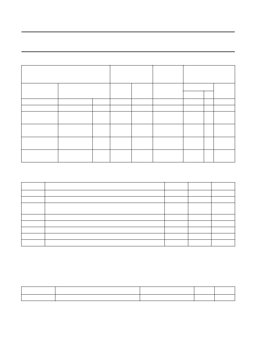
QUICK REFERENCE DATA
Note
1. When digital mode is selected, V
DDA
supply pins can be connected to ground.
SYMBOL
PARAMETER
CONDITIONS
MIN.
TYP.
MAX.
UNIT
V
DDD
digital supply voltage
3
5
5.25
V
V
DDA
analog supply voltage
3
5
5.25
V
V
IL
LOW level digital input voltage
0
-
0.3V
DDD
V
V
IH
HIGH level digital input voltage
0.6V
DDD
-
V
DDD
V
V
OL
LOW level digital output voltage I
OL
=
-
20
µ
A
-
-
0.5
V
V
OH
HIGH level digital output voltage I
OH
= 20
µ
A
V
DDD
-
0.1
-
-
V
I
DDD(tot)
total digital supply current
f
clk
= 14.3 MHz; V
DDD
= 5 V
-
180
200
mA
f
clk
= 14.3 MHz; V
DDD
= 3.3 V
-
80
100
mA
I
DDA(tot)
total analog supply current
f
clk
= 14.3 MHz; V
DDA
= 5 V
-
30
40
mA
f
clk
= 14.3 MHz; V
DDA
= 3.3 V
-
22
35
mA
T
amb
operating ambient temperature
0
-
75
∞
C
I
DMD
supply current in digital output
mode
f
clk
= 14.3 MHz; V
DDD
= 5 V;
note 1
-
185
-
mA
f
clk
= 14.3 MHz; V
DDD
= 3.3 V
-
85
-
mA

1997 Jun 13
4
Philips Semiconductors
Preliminary specification
Digital Signal Processor (DSP) for
cameras
SAA8110G
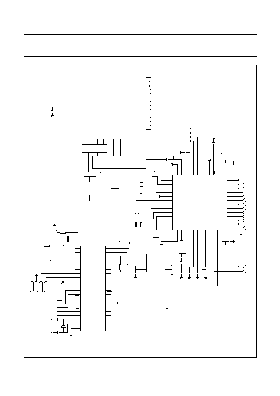
BLOCK DIAGRAM
full pagewidth
MGK158
7 to 16
CCD9
to
CCD0
CLK1
V
DDD(C1)
V
DDD(C2)
V
DDD(C3)
V
DDD(P1)
V
DDD(P2)
V
SSD(C1)
V
SSD(C2)
V
SSD(C3)
V
SSD(C4)
V
SSD(P1)
V
SSD(P2)
V
DDA(BG)
V
DDA(DC)
V
DDA(CD)
V
DDA(O1)
V
DDA(O2)
V
DDA(O3)
V
SSA(CD)
V
SSA(OB)
V
SSA(BG)
1, 29,72,
46, 62
6, 17, 76,
78, 53, 71
45, 41, 22,
40, 38, 36
19, 34,
42
OFFSET
PRE-
PROCESSING
RGB
SEPARATION
(INCL. LINE
MEMORIES)
RGB
PROCESSING
DIGITAL
OUTPUT
FORMATTER
ANALOG
OUTPUT
PREPROCESSING
PAL/NTSC-
ENCODER
V DACs
Y-
PROCESSING
UV-
PROCESSING
RGB
TO
YUV
2
CLK2
47
RESET
31 to 33
T2, T1, T0
MODE
CONTROL
MISCELLANEOUS
FUNCTIONS
SAA8110G
MEASUREMENT ENGINE
30
20
21
25
26,
27
23
24
18
SCLK
CDAC
OUT
CDAC
RBIAS
SDATA
STROBE
SMP
P0, P1
VH-REFERENCE WINDOW
TIMING AND CONTROL
34
5
FI
IN
73
77
75
74
VSYNC
IN
HSYNC
IN
SCL/SN
CL
SDA
A0/SN
DA
A1/SN
RES
SNERT/I
2
C
INTERFACE
SNERT/
I
2
C
SELECT
Y0 to Y7
UV0 to UV7
70 to 63
43
VSYNC
OUT
44
HREF
28
80
49
50
48
52
51
61 to 54
OUT3 to OUT1
DECOUPL
RBIAS
SIS
79
X
IN
X
OUT
35, 37, 39
LLC
CREF/PXQ
FI
OUT
Fig.1 Block diagram.

1997 Jun 13
5
Philips Semiconductors
Preliminary specification
Digital Signal Processor (DSP) for
cameras
SAA8110G
PINNING
SYMBOL
PIN
I/O
DESCRIPTION
V
DDD(C1)
1
I
digital supply 1 for digital core and CLK1 related peripherals
CLK1
2
I
system- or pixel clock
VSYNC
IN
3
I
vertical synchronization input
HSYNC
IN
4
I
horizontal synchronization input
FI
IN
5
I
field identification signal input
V
SSD(C1)
6
I
digital ground 1 for digital core and CLK1 related peripherals
CCD9
7
I
(preprocessed) AD-converted CDD-signal bit 9 (MSB)
CCD8
8
I
(preprocessed) AD-converted CDD-signal bit 8
CCD7
9
I
(preprocessed) AD-converted CDD-signal bit 7
CCD6
10
I
(preprocessed) AD-converted CDD-signal bit 6
CCD5
11
I
(preprocessed) AD-converted CDD-signal bit 5
CCD4
12
I
(preprocessed) AD-converted CDD-signal bit 4
CCD3
13
I
(preprocessed) AD-converted CDD-signal bit 3
CCD2
14
I
(preprocessed) AD-converted CDD-signal bit 2
CCD1
15
I
(preprocessed) AD-converted CDD-signal bit 1
CCD0
16
I
(preprocessed) AD-converted CDD-signal bit 0 (LSB)
V
SSD(C2)
17
I
digital ground 2 for digital core and CLK1 related peripherals
SCLK
18
O
serial clock to TDA8786
V
SSA(CD)
19
I
analog ground for control DAC
CDAC
OUT
20
O
output control DAC
CDAC
RBIAS
21
I
pin to connect external bias resistor for control DAC
V
DDA(CD)
22
I
analog supply for control DAC
SDATA
23
O
serial data to TDA8786
STROBE
24
O
strobe to TDA8786
SMP
25
O
switch mode pulse for DC-DC
P0
26
O
quasi-static control output pin 0
P1
27
O
quasi-static control output pin 1
SIS
28
I
SNERT/I
2
C-bus select input signal
V
DDD(C2)
29
I
digital supply 2 for digital core and CLK1 related peripherals
RESET
30
I
reset input
T2
31
I
test mode control signal bit 2
T1
32
I
test mode control signal bit 1
T0
33
I
test mode control signal bit 0
V
SSA(OB)
34
I
analog ground for the three output buffers
OUT3
35
O
output buffer 3 (R, V or CVBS)
V
DDA(O3)
36
I
analog supply for output buffer OUT3
OUT2
37
O
output buffer 2 (B, U or C)
V
DDA(O2)
38
I
analog supply for output buffer OUT2
OUT1
39
O
output buffer 1 (G or Y)
V
DDA(O1)
40
I
analog supply for output buffer OUT1

1997 Jun 13
6
Philips Semiconductors
Preliminary specification
Digital Signal Processor (DSP) for
cameras
SAA8110G
V
DDA(DC)
41
I
analog supply for analog core of triple DAC
V
SSA(BG)
42
I
analog ground for to band gap
DECOUPL
43
O
pin to be used for external decoupling of band gap
RBIAS
44
O
external bias resistor connection for band gap
V
DDA(BG)
45
I
analog supply for band gap
V
DDD(P1)
46
I
digital supply 1 for CLK2 related peripherals
CLK2
47
I
output clock (CLK2 frequency is 2
◊
CLK1 frequency)
FI
OUT
48
O
field identification output pulse
VSYNC
OUT
49
O
vertical synchronization output
HREF
50
O
horizontal reference output for YUV-port
CREF/PXQ
51
O
clock/pixel qualifier output for YUV-port
LLC
52
O
line-locked system clock output
V
SSD(P1)
53
I
digital ground 1 for CLK2 related peripherals
UV7
54
O
multiplex chrominance UV bit 7 (MSB)
UV6
55
O
multiplex chrominance UV bit 6
UV5
56
O
multiplex chrominance UV bit 5
UV4
57
O
multiplex chrominance UV bit 4
UV3
58
O
multiplex chrominance UV bit 3
UV2
59
O
multiplex chrominance UV bit 2
UV1
60
O
multiplex chrominance UV bit 1
UV0
61
O
multiplex chrominance UV bit 0 (LSB)
V
DDD(P2)
62
I
digital supply for CLK2 related peripherals
Y7
63
O
luminance Y or multiplexed YUV bit 7 (MSB)
Y6
64
O
luminance Y or multiplexed YUV bit 6
Y5
65
O
luminance Y or multiplexed YUV bit 5
Y4
66
O
luminance Y or multiplexed YUV bit 4
Y3
67
O
luminance Y or multiplexed YUV bit 3
Y2
68
O
luminance Y or multiplexed YUV bit 2
Y1
69
O
luminance Y or multiplexed YUV bit 1
Y0
70
O
luminance Y or multiplexed YUV bit 0 (LSB)
V
SSD(P2)
71
I
digital ground 2 for to CLK2 related peripherals
V
DDD(C3)
72
I
digital supply 3 for digital core and CLK1 related peripherals
A1/SN
RES
73
I
I
2
C-bus address select pin A1 or SNERT reset input
A0/SN
DA
74
I
I
2
C-bus address select pin A0 or SNERT data input/output
SDA
75
I
I
2
C-bus data input/output
V
SSD(C3)
76
I
digital ground 3 for digital core and CLK1 related peripherals
SCL/SN
CL
77
I
I
2
C-bus clock/SNERT clock input
V
SSD(C4)
78
I
digital ground 4 for digital core and CLK1 related peripherals
X
IN
79
I
input crystal oscillator for subcarrier lock applications
X
OUT
80
O
output crystal oscillator for subcarrier lock applications
SYMBOL
PIN
I/O
DESCRIPTION

1997 Jun 13
7
Philips Semiconductors
Preliminary specification
Digital Signal Processor (DSP) for
cameras
SAA8110G
Fig.2 Pin configuration.
handbook, full pagewidth
SAA8110G
MGK151
1
2
3
4
5
6
7
8
9
10
11
12
13
14
15
16
17
18
19
20
60
59
58
57
56
55
54
53
52
51
50
49
48
47
46
45
44
43
42
41
UV1
UV2
UV3
UV4
UV5
UV6
UV7
VSSD(P1)
LLC
CREF/PXQ
HREF
VSYNCOUT
FIOUT
CLK2
VDDD(P1)
VDDA(BG)
RBIAS
DECOUPL
VSSA(BG)
VDDA(DC)
VDDD(C1)
CLK1
VSYNCIN
HSYNCIN
FIIN
VSSD(C1)
CCD9
CCD8
CCD7
CCD6
CCD5
CCD4
CCD3
CCD2
CCD1
CCD0
VSSD(C2)
SCLK
VSSA(CD)
CDACOUT
21
22
23
24
25
26
27
28
29
30
31
32
33
34
35
36
37
38
39
40
80
79
78
77
76
75
74
73
72
71
70
69
68
67
66
65
64
63
62
61
X
OUT
X
IN
V
SSD(C4)
SCL/SN
CL
V
SSD(C3)
SDA
A0/SN
DA
A1/SN
RES
V
DDD(C3)
V
SSD(P2)
Y0
Y1
Y2
Y3
Y4
Y5
Y6
Y7
V
DDD(P2)
UV0
CDAC
RBIAS
V
DDA(CD)
SDATA
STROBE
SMP
P0
P1
SIS
V
DDD(C2)
RESET
T2
T1
T0
V
SSA(OB)
OUT3
V
DDA(O3)
OUT2
V
DDA(O2)
OUT1
V
DDA(O1)

1997 Jun 13
8
Philips Semiconductors
Preliminary specification
Digital Signal Processor (DSP) for
cameras
SAA8110G
FUNCTIONAL DESCRIPTION
Black offset preprocessing
The input data is clamped within the optical black pixel
area of the CCD. The size of the digital clamp window is
16 pixels by 128 lines (i.e. TDA8786). It is possible to
differentiate black levels for odd/even lines, pixels and
fields. This comes in addition to the analog preprocessing
clamp which is active on the clamp pulse generated by the
external timing circuit. The analog clamp is included in the
TDA8786.
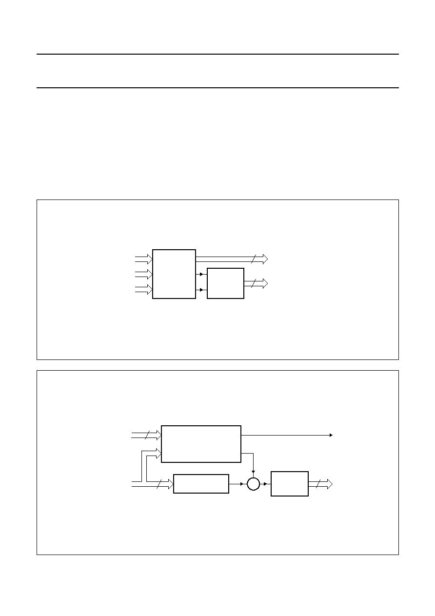
RGB separation
PAL/NTSC sensors generate interlaced data adding offset
in the complementary colour pixels. The RGB separation
block with its two line memories generates the three
components Y, 2R
-
G, and 2B
-
G for each input data
corresponding to a pixel value of the CCD. Then the
triplet R, G, B is derived. This block also delivers some
contour and white clip information.
RGB processing
The RGB processing includes several features:
∑
Colour space matrix depending on CCD type to be
suitable with different sensor colour filters
∑
Gain correction for R and B signals for white balance
control
∑
Black offset
∑
Adjustable knee
∑
Adjustable gamma function.
The knee function is applied to all three RGB signals.
Its shape is continuously adjustable by changing the slope
and the knee offset point.
To compensate for the non-linear response of display
devices, a gamma correction is applied to R, G and B
signals. It may be adjustable from linear to a 0.35 power
coefficient.
Fig.3 RGB separation diagram.
handbook, full pagewidth
MGK153
LINE
MEMORY
LINE
MEMORY
R
G
B
CCD inputs
white clip
vertical contour
RGB
COLOUR
SEPARATION
10
Fig.4 RGB processing.
handbook, full pagewidth
MGK154
COLOUR
MATRIX
R
Rgain
Rblack
Gblack
G
B
3
◊
KNEE
R
G
B
+
◊
+
Bgain
Bblack
◊
+
3
◊
GAMMA
1997 Jun 13
9
Philips Semiconductors
Preliminary specification
Digital Signal Processor (DSP) for
cameras
SAA8110G
RGB-to-YUV block
After RGB processing, the channels are separated in a
luminance and two colour difference path:
Y = 0.299 R + 0.597 G + 0.114 B, U = 0.49 (B
-
Y) and
V = 0.88 (R
-
Y) . It also contains two down-sampling
filters for U and V signals.
Y-processing
The luminance component includes several features:
∑
Contour correction allowing an increase of the
luminance transitions for a sharper picture
∑
Black stretch function for contrast enhancement in dark
scenes
∑
False colour detector used by the UV-processing block
to enable the colour killer
∑
Filters and noise reduction by coring (only in the high
frequency part of the signal).
Fig.5 RGB-to-YUV conversion.
handbook, full pagewidth
MGK155
Y
(0 to 511)
CONVERSION
MATRIX
DOWN-
SAMPLING
& MUX
9
R
G
B
UV
(
-
128 to 127)
8
Fig.6 Y processing.
handbook, full pagewidth
MGK156
NOISE
REDUCTION
CONTOUR PROCESSING
AND
FALSE COLOUR DETECTION
BLACK STRETCH
false colour
Y
(0, 0.5 to 255.5)
Y
8
+
9
vertical contour
(
-
512 to 511)
(from RGB-separation)
10

1997 Jun 13
10
Philips Semiconductors
Preliminary specification
Digital Signal Processor (DSP) for
cameras
SAA8110G
Fig.7 UV-processing.
handbook, full pagewidth
MGK157
UV GAIN
CONTROL
FALSE COLOUR
CORRECTION
NOISE
REDUCTION
false colour
(from Y-processing)
white clip
(from RGB-separation)
UV
(
-
127 to 128)
8
UV
(
-
127 to 128)
8
UV-processing
The chrominance component includes several features:
∑
Noise reduction for high frequencies
∑
False colour correction: a colour killer cuts the false
colour components in the UV signals
∑
UV-gain control used to set the correct UV levels for
PAL/NTSC encoding.
As the colour filter saturation levels may be different in the
CCD, the white clip is used in the UV-processing to
suppress colour errors in case of high exposure.
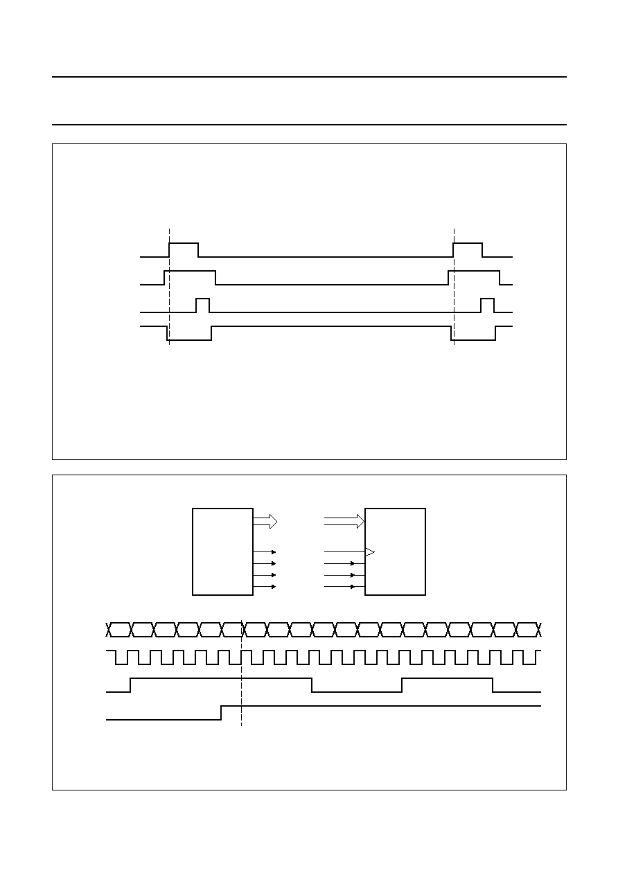
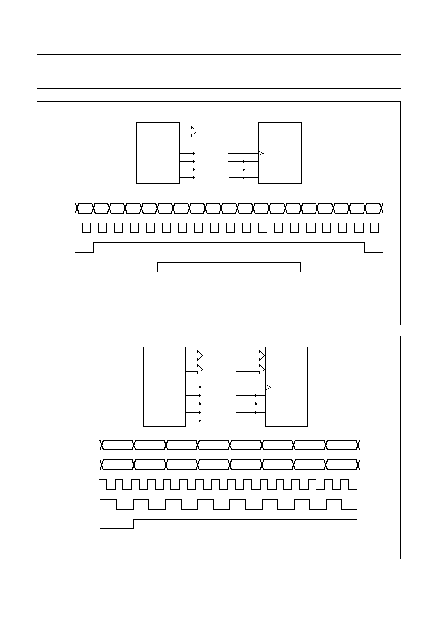
Digital output formatter
This block contains several features:
∑
Generation of a synchronous clock LLC (twice the clock
frequency)
∑
Generation of three synchronization signals (HREF,
CREF and VS)
∑
Synchronization of the output data to the output clock
LLC
∑
Generation of a CIF/QCIF output format for several type
of sensors (see Table 1)
∑
Selection of the required digital output format (8-bit
multiplexed YUV standard D1/CCIR 656, including the
generator of SAV/EAV codes or 16-bit multiplexed YUV
4 : 2 : 2 standard DTV2/CCIR601).
Note that the D1 frequency data rate is twice the DTV2
frequency data rate.
Moreover, using a high resolution PAL and NTSC CCDs,
it is possible to generate the following formats by means of
cutting or down-sampling.
∑
CIF 352
◊
288 at 25 frame/second and CIF 352
◊
240 at
30 frame/second
∑
QCIF 176
◊
144 at 25 frame/second and QCIF
176
◊
120 at 30 frame/second.
Table 1
CIF/QCIF output format for different sensor
types
INPUT FORMAT
OUTPUT FORMAT
PAL/NTSC-sensor
CIF
`full screen'
CIF
`zoom-by-2'
QCIF
`full screen'
QCIF
`zoom-by-2'
QCIF
`zoom-by-4'
CIF
QCIF
`full screen'
QCIF
`zoom-by-2'
1997 Jun 13
11
Philips Semiconductors
Preliminary specification
Digital Signal Processor (DSP) for
cameras
SAA8110G
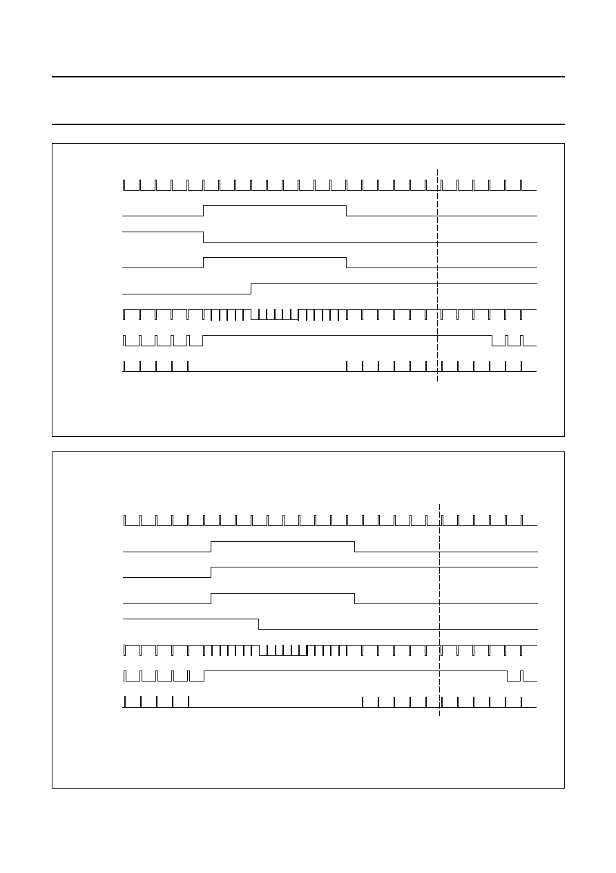
Fig.8 Vertical timing NTSC odd field.
handbook, full pagewidth
MGK159
HSYNCIN
VSYNCIN
FIIN
FIOUT
VSYNCOUT
CSYNC
BLANK
BURST
521
523
525
2
4
6
8
10
12
14
18
20
522
524
1
3
5
7
9
11
13
15
19
21
22
23
Fig.9 Vertical timing NTSC even field.
handbook, full pagewidth
MGK160
HSYNCIN
VSYNCIN
FIIN
FIOUT
VSYNCOUT
CSYNC
BLANK
BURST
258
260
262
264
266
268
270
272
274
276
280
282
259
261
263
265
267
269
271
273
275
277
281
283 284 285

1997 Jun 13
12
Philips Semiconductors
Preliminary specification
Digital Signal Processor (DSP) for
cameras
SAA8110G
Fig.10 Vertical timing PAL odd field.
handbook, full pagewidth
HSYNCIN
VSYNCIN
FIIN
FIOUT
VSYNCOUT
CSYNC
BLANK
BURST
(1)
even frame
odd frame
- +
+
-
+
-
+
-
+
-
+
-
+
-
+
+
-
621 622 623 624 625
2
4
6
8
10
12
14
20
22
1
3
5
7
9
11
13
15
2 1
23
24
25
MGK161
odd frame
+
+
-
even frame
+
-
+
-
+ -
+
-
+
-
+
-
+
-
(1) +: burst phase = +135
∞
.
-
: burst phase =
-
135
∞
.
Fig.11 Vertical timing PAL even field.
(1) +: burst phase = +135
∞
.
-
: burst phase =
-
135
∞
.
handbook, full pagewidth
HSYNCIN
VSYNCIN
FIIN
FIOUT
VSYNCOUT
CSYNC
BLANK
BURST
(1)
odd frame
- +
+
-
+
-
+
-
+
-
+
-
+
-
+
+
-
308 309 310 311 312
314
316
313
315
317 318 319 320 321
332
334
336
333
335
337
322
324
326
323
325
327
MGK162
even frame
+
-
+
-
+ -
+
-
+
-
+
-
+
-
+
-
+
1997 Jun 13
13
Philips Semiconductors
Preliminary specification
Digital Signal Processor (DSP) for
cameras
SAA8110G
Fig.12 Horizontal timing for non-CIF processing.
handbook, full pagewidth
MGK163
0
NPIX
HSYNCIN
HREF
BLANK
BURST
Fig.13 8-bits multiplexed format (D1, CCIR656); example: CIF down-sampling.
handbook, full pagewidth
MGK164
SAA8110G
(OUTPUTS
CLOCKED
AT
CLK2)
HOST
LLC
YUV
PXQ
HREF
VSYNCOUT
LLC
Y(UV)
FF
00
00
SAV
U0
Y0
V0
Y2
U4
Y4
V4
Y6
PXQ
HREF
sample moment
Y(UV)7
to
Y(UV)0
1997 Jun 13
14
Philips Semiconductors
Preliminary specification
Digital Signal Processor (DSP) for
cameras
SAA8110G
Fig.14 8-bits multiplexed format (D1, CCIR656); SAV/EAV included.
handbook, full pagewidth
SAA8110G
(OUTPUTS
CLOCKED
AT
CLK2)
HOST
LLC
Y(UV)7
to
Y(UV)0
YUV
MGK165
PXQ
HREF
VSYNCOUT
LLC
YUV
FF
00
00
SAV
FF
00
00
EAV
U0
Y0
V0
Y1
U2
Y2
V2 UN
-
1 YN
-
1
PXQ
HREF
sample moment
Fig.15 16-bits multiplexed format (DTV2, CCIR601).
handbook, full pagewidth
MGK166
SAA8110G
(OUTPUTS
CLOCKED
AT
CLK2)
HOST
LLC
UV
UV7 to UV0
Y(UV)
Y7 to Y0
CREF
HREF
VSYNCOUT
FIOUT
LLC
Y(UV)
U0
Y2
Y1
Y0
V0
Y3
U6
Y6
Y5
Y4
U4
V4
U2
V2
CREF
HREF
sample moment
UV

1997 Jun 13
15
Philips Semiconductors
Preliminary specification
Digital Signal Processor (DSP) for
cameras
SAA8110G
Analog output preprocessing
This block contains several features:
∑
Delay compensation for the luminance signal
∑
Up-sampling of the UV signal
∑
PAL/NTSC encoding
∑
YUV to RGB conversion
∑
Selection of the required analog output format (RGB,
YUV, YC or CVBS).
The analog outputs are given by three voltage DACs in
RGB or YUV or CVBS or YC format. Channels Y and G
include the sync information. Over-sampling at twice f
clk
is
made so that external filtering becomes easier. It is also
possible to have an adjustment of the subcarrier via the
serial interface. When CVBS output is used, chrominance
range is halved compared to luminance.
Measurement engine
The measurement engine performs measurements on
some selectable internal signals on frame/field basis and
prepares data for auto exposure, auto focus and auto
white balance processing. It uses an internal RAM
work-space for its control and data handling operations.
The contents of the work-space can be accessed via the
serial interface.
Vertical/horizontal reference and window timing and
control
The SAA8110G uses two vertical and horizontal
synchronization input signals (VSYNC
IN
and HSYNC
IN
) to
derive internal vertical and horizontal reference signals.
Besides a Field Identification input (FI
IN
) signal is required.
The timing of the vertical and horizontal input signals
should be such that:
1. The pixel frequency (CLK1) must be line-locked to the
line frequency of HSYNC
IN
: the number of clock
periods between two HSYNC
IN
pulses must be a fixed
integer number. The HSYNC
IN
should be at least one
clock period active HIGH.
2. The VSYNC
IN
signal indicates the start of a field
(or frame in case of progressive scanning); this
signal is also required for non-interlaced applications.
The VSYNC
IN
should be at least one clock period
HIGH.
3. The FI
IN
pulse indicates the phase of the field in case
of interlaced applications (FI
IN
= 0 means odd field).
Serial interface
The serial interface can either be an I
2
C-bus or a 80C51
UART (SNERT) (selectable with the SIS pin). Via the serial
interface the external microcontroller can control the
internal settings of the SAA8110G and read/write from/to
the internal RAM work-space linked to the measurement
engine (see list of parameter settings in
Chapter "Programming"). Some of the registers are
double-buffered to prevent that the change of control data
becomes visible on the output display.
Miscellaneous functions
A three wire bus is used to send 10-bit settings from a
microcontroller to the TDA8786 via the SAA8110G
registers.The SAA8110G supplies picture parameters and
needs some configuration parameters. Those values are
contained in registers and are updated during every
vertical synchronization pulse.
Mode control
This block controls the operation mode of the SAA8110G.
As described in Table 2, four modes may be selected:
depending on power reduction and I
2
C-bus timing.
Power dissipation management
The power dissipation of the SAA8110G will depend on the
required activity for a certain application. It is possible to
switch off via the serial interface unconcerned parts for a
given application. When an analog output is not used, the
power voltage pin of the DAC can be connected to ground
to limit the power consumption.
Clock configurations
Following conditions must be fulfilled:
∑
CLK1 should be generated as divide-by-two from CLK2
∑
The RESET pin should not go LOW before CLK1 and
CLK2 are both HIGH or LOW.
Table 2
SAA8110G mode control
T2
T1
T0
MODE
POWER
REDUCTION
t
o(h)
I
2
C-BUS
0
0
0
application
mode
on
short
0
0
1
on
long
0
1
0
off
short
0
1
1
off
long
1997 Jun 13
16
Philips Semiconductors
Preliminary specification
Digital Signal Processor (DSP) for
cameras
SAA8110G
Table 3
Sensor and output formats covered by the SAA8110G
LIMITING VALUES
In accordance with the Absolute Maximum Rating System (IEC134).
HANDLING
Inputs and outputs are protected against electrostatic discharge in normal handling. However, to be totally safe, it is
desirable to take normal precautions appropriate to handling MOS devices.
THERMAL CHARACTERISTICS
CCD-formats
RESOLUTION
PIXEL
FREQUENCY
(MHz)
OUTPUT FORMATS
STANDARD
FRAME SCANNING AND
FREQUENCY (Hz)
ACTIVE
H/V
TOTAL
H/V
DIGITAL
ANALOG
DTV2/D1 CIF
CIF
non-interlaced
60
352/243
429/262
6.75
no
yes
yes
CIF
non-interlaced
50
352/288
432/312
6.75
no
yes
yes
NTSC
high resolution
non-interlaced
60.054
768/243
910/262
14.3181
yes
yes
yes
interlaced
29.997
768/494
910/525
PAL
high resolution
non-interlaced
50
752/288
908/312
14.1875
yes
yes
yes
interlaced
25
752/582
908/625
NTSC
medium resolution
non-interlaced
60
512/243
606/262
9.53495
yes
no
yes
interlaced
30
512/492
606/525
PAL
medium resolution
non-interlaced
50
512/288
618/312
9.65625
yes
no
yes
interlaced
25
512/582
618/625
SYMBOL
PARAMETER
MIN.
MAX.
UNIT
V
DDD
digital supply voltage
-
0.3
+7.0
V
V
DDA
analog supply voltage
-
0.3
+7.0
V
V
DDD-DDA
supply voltage difference between the digital and the analog
supply voltages
-
0.1
+0.1
V
V
I
input voltage
-
0.3
V
DD
+ 0.3
V
V
O
output voltage
-
0.3
V
DD
+ 0.3
V
P
tot
total allowed power dissipation at T
amb
= 75
∞
C
-
1
W
T
stg
storage temperature
-
55
+150
∞
C
T
j
junction temperature
-
125
∞
C
SYMBOL
PARAMETER
CONDITIONS
VALUE
UNIT
R
th(j-a)
thermal resistance from junction to ambient
in free air
50
K/W
1997 Jun 13
17
Philips Semiconductors
Preliminary specification
Digital Signal Processor (DSP) for
cameras
SAA8110G
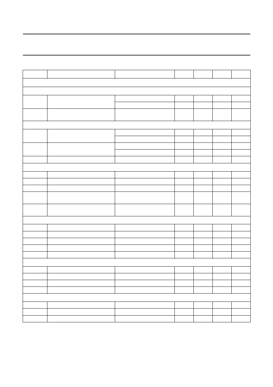
CHARACTERISTICS
SYMBOL
PARAMETER
CONDITIONS
MIN.
TYP.
MAX.
UNIT
VDACs specification
O
UTPUTS PINS
OUT1
TO
OUT3 (
IN CASE OF SCALE FACTOR
= 1)
V
o
output voltage (see note 1)
code 0
0
0.2
0.3
V
code 511
1.3
1.5
1.6
V
V
offset
amplitude offset voltage between
DACs
-
60
+60
mV
I
NPUTS
R
bias
bias resistor
note 2
14
15
16
k
note 3
44
47
50
k
R
ext
external anti-reflection resistor
note 2
-
21
-
note 3
-
70.6
-
C
decoup
decoupling capacitor
10
-
100
nF
T
RANSFER FUNCTION
RES
resolution
-
9
-
bit
NL
diff
differential non-linearity
-
-
1.5
LSB
NL
int
integral non-linearity
-
-
1.5
LSB
THD
60
total harmonic distortion at 60%
of full-scale
f
clk
= 30 MHz, f
i
= 1 MHz,
V
DDA
= 5 V
-
55
45
dB
S/N
signal-to-noise ratio
f
clk
= 30 MHz, f
o
= 1 MHz,
V
DDA
= 5 V
-
45
38
dB
A
PPLICATION
1: PAL/NTSC
HIGH RESOLUTION
V
DD1
supply voltage
4.5
5.0
5.5
V
V
DD2
supply voltage
3.0
3.3
3.6
V
CR
conversion rate
-
28.6
-
MHz
f
clk
clock frequency
-
28.6
-
MHz
B
a
analog bandwidth
-
7.6
-
MHz
A
PPLICATION
2: PAL/NTSC
MEDIUM RESOLUTION
V
DD1
supply voltage
4.5
5.0
5.5
V
V
DD2
supply voltage
3.0
3.3
3.6
V
f
clk
clock frequency
-
19
-
MHz
B
a
analog bandwidth
-
6.5
-
MHz
S
WITCHING CHARACTERISTICS ON RISING FULL
-
SCALE STEP
(see Fig.16)
t
PD
propagation delay time
to 50% value
-
9
13
ns
t
st(10-90)
settling time
10% to 90% full-scale
-
9
11
ns
t
st(LSB)
setting time (to
±
1 LSB)
-
25
30
ns

1997 Jun 13
18
Philips Semiconductors
Preliminary specification
Digital Signal Processor (DSP) for
cameras
SAA8110G
Notes
1. When CVBS output is used the chrominance range is halved compared to luminance.
2. Monitor load of 75
with R
ext
= 21
and R
bias
= 15 k
at 3.3 V application.
3. Monitor load of 75
with R
ext
= 70.6
and R
bias
= 47 k
at 5.0 V application.
CDAC specification (V
DD
= 5 V)
L
int
integral linearity
-
-
1
LSB
L
diff
differential linearity
-
-
1
/
2
LSB
V
o(CDAC)
output voltage at pin CDAC
code 0
-
10
300
mV
code 61, V
DDA
= 5 V
-
4.6
4.95
-
V
code 61, V
DDA
= 3.3 V
3
3.25
-
V
R
o(CDAC)
output resistance at pin CDAC
-
13
-
f
clk
clock frequency
-
28.6
-
MHz
R
L
load resistance
-
10
-
k
C
L
load capacitance
-
-
10
pF
t
PD
propagation delay time
to 50% value (see Fig.17),
V
DDA
= 5 V
-
-
104
ns
t
st(10-90)
settling time
10% to 90% full-scale (see
Fig.16)
-
9
-
ns
t
st(LSB)
setting time
to
±
1 LSB (see Fig.16)
-
25
-
ns
I
NPUTS RELATED TO
CLK1: CCD0
TO
CCD9, VSYNC
IN
, HSYNC
IN,
FI
IN
t
su(i)(D)1
data input set-up time CCD
inputs, HSYNC
IN
, VSYNC
IN
, FI
IN
0
3
5
ns
t
su(i)(D)2
data input set-up time SN
RES
and
SN
DA
0
1
2
ns
t
h(i)(CCD)
data hold time CCD inputs
-
1
-
+1
ns
t
h(i)(D)
data input hold time
VSYNC
IN
, HSYNC
IN
, FI
IN
0
1
3
ns
O
UTPUTS RELATED TO
CLK2: Y7
TO
Y0, UV7
TO
UV0, CREF, HREF, VSYNC
OUT
, FI
OUT
AND
LLC
t
h(o)(D)
data output hold time
-
8
22
ns
t
d(o)(D)
data output delay time
-
25
31
ns
O
UTPUTS RELATED TO
CLK1: SDATA, STROBE, SMP, P0, P1
AND
SCLK
t
h(o)(D)
data output hold time
-
13
21
ns
t
d(o)(D)
data output delay time
-
15
24
ns
clk
clock duty cycle
40
-
60
%
SYMBOL
PARAMETER
CONDITIONS
MIN.
TYP.
MAX.
UNIT

1997 Jun 13
19
Philips Semiconductors
Preliminary specification
Digital Signal Processor (DSP) for
cameras
SAA8110G
Fig.16 Switching characteristics.
handbook, full pagewidth
CLK2
(code 0)
code 0
(code FS)
code FS
input code
(example of a full-scale
input data transmission)
1 LSB
1 LSB
90%
50%
10%
MGK167
tPD
tst(10
-
90)
tst(LSB)
Fig.17 Data input/output timing.
handbook, full pagewidth
MGK168
CLK1
DATA IN
DATA OUT
tPD
th(i)(D)
tsu

1997 Jun 13
20
Philips Semiconductors
Preliminary specification
Digital Signal Processor (DSP) for
cameras
SAA8110G
PROGRAMMING
Overview available write
ADDRESS
SYMBOL
FUNCTION
FORMAT
RANGE/VALUE
0
CONTROL0
miscellaneous; see Table 4
byte
n.a.
1
CONTROL1
miscellaneous; see Table 5
(1)
byte
n.a.
2
CONTROL2
miscellaneous; see Table 6
byte
n.a.
4
OB_STARTL_F0
first line optical black window in field 0
byte
0 to 255
5
OB_STARTL_F1
first line optical black window in field 1/frame
byte
0 to 255
7
OB_STARTP
first pixel optical black window
byte
0 to 255
8
OB_PE_F0
fixed optical black level for even pixel in field 0
byte
0
9
OB_PO_F0
fixed optical black level for odd pixel in field 0
byte
0
10
OB_PE_F1
fixed optical black level for even pixel in
field 1/frame
byte
0
11
OB_PO_F1
fixed optical black level for odd pixel in
field 1/frame
byte
0
12
OB_OFFSET_LE
optical black offset for even line
byte
0
13
OB_OFFSET_LO
optical black offset for odd line
byte
0
14
MOSAIC_SEP_S1
multiplication-factor for Yn at even line and even
pixel
byte
0 to 255
15
MOSAIC_SEP_S2
multiplication-factor for Yn at even line and odd
pixel
byte
0 to 255
16
MOSAIC_SEP_S3
multiplication-factor for Yn at odd line and even
pixel
byte
0 to 255
17
MOSAIC_SEP_S4
multiplication-factor for Yn at odd line and odd
pixel
byte
0 to 255
18
WHITE_CLIP_THR
threshold for white clip
byte
768 to 1023
19
COL_MAT_P11
colour matrix coefficient p11
byte
-
128 to 127
20
COL_MAT_P12
colour matrix coefficient p12
byte
-
128 to 127
21
COL_MAT_P13
colour matrix coefficient p13
byte
-
128 to 127
22
COL_MAT_P21
colour matrix coefficient p21
byte
-
128 to 127
23
COL_MAT_P22
colour matrix coefficient p22
byte
-
128 to 127
24
COL_MAT_P23
colour matrix coefficient p23
byte
-
128 to 127
25
COL_MAT_P31
colour matrix coefficient p31
byte
-
128 to 127
26
COL_MAT_P32
colour matrix coefficient p32
byte
-
128 to 127
27
COL_MAT_P33
colour matrix coefficient p33
byte
-
128 to 127
28
COL_MAT_RGAIN
colour matrix R-gain factor
(1)
byte
0 to 255
29
COL_MAT_BGAIN
colour matrix B-gain factor
(1)
byte
0 to 255
34
BLACK_LEVEL_R
fixed R-black level offset
(1)
byte
-
128 to 127
35
BLACK_LEVEL_G
fixed G-black level offset
(1)
byte
-
128 to 127
36
BLACK_LEVEL_B
fixed B-black level offset
(1)
byte
-
128 to 127
37
RGB_KNEE_OFFSET offset for RGB-knee
(1)
byte
0 to 255
38
GAMMA_BALANCE
gamma multiplication factor (LS)
(1)
6 bits
0 to 63

1997 Jun 13
21
Philips Semiconductors
Preliminary specification
Digital Signal Processor (DSP) for
cameras
SAA8110G
39
NPIX_LSB
number of pixels on a line
byte
0 to 255
40
NPIX_MSB
number of pixels on a line
2 bits
0 to 3
41
FPIX_ACT
number of first active pixel on a line
byte
0 to 255
42
LPIX_ACT_LSB
number of last active pixel on a line
byte
0 to 255
43
FLINE_ACT_F0
number of first active line in field 0
byte
0 to 255
44
LLINE_ACT_F0_LSB
number of last active line in field 0
byte
0 to 255
45
FLINE_ACT_F1_LSB
number of first active line in field 1/frame
byte
0 to 255
46
LLINE_ACT_F1_LSB
number of last active line in field 1/frame
byte
0 to 255
47
ACT_LINES_MSB
MSBs of active line numbers
byte
see Table 7
48
CTR_UPD_LINE
number of line for double buffered update control
registers
byte
0 to 255
49
KCOMB
vertical contour comb filter coefficient (MS)
3 bits
0 to 7
VCGAIN
vertical contour gain (LS)
4 bits
0 to 15
50
CLDLEV
contour level dependancy level
(1)
byte
0 to 255
51
HCHGAIN
horizontal contour band pass filter high gain (MS)
4 bits
0 to 15
HCLGAIN
horizontal contour band pass filter low gain (LS)
4 bits
0 to 15
52
CNCLEV
contour noise coring level
(1)
6 bits
0 to 63
53
CONGAIN
contour gain factor
byte
0 to 63
54
FCDLEV
false colour detect level
byte
0 to 255
55
YNCLEV
Y (luminance) noise coring level
byte
0 to 127
56
YGAIN
Y (luminance) gain factor
(1)
byte
0
57
YCMPDEL
Y (luminance) compensation delay
4 bits
-
3 to 4
see Table 8
58
UVNCLEV
UV (chrominance) noise coring level
byte
0 to 255
59
UGAIN
U(B
-
Y) gain factor
(1)
byte
0
60
VGAIN
V(R
-
Y) gain factor
(1)
byte
0
61
DTO_FREQ_LSB
DTO frequency (MSB)
(1)
byte
0 to 255
62
DTO_FREQ_ISB
DTO frequency
(1)
byte
0 to 255
63
DTO_FREQ_MSB
DTO frequency (LSB)
(1)
byte
0 to 255
64
PHASESHIFT
PHASE_SHIFT colour subcarrier
byte
0 to 255
65
BURST_LEVEL
BURST_LEVEL colour burst
byte
0 to 255
66
A
AWB_A (ME)
byte
-
98
pole_thresh #A (DPD)
byte
0 to 255
67
B
AWB_B (ME); pole_thresh #B (DPD)
byte
-
104
68
C
AWB_C (ME); pole_thresh #A (DPD)
byte
-
68
69
D
AWB_D (ME); pole_thresh #B (DPD)
byte
126
70
E
AWB_E (ME)
6 bits
63
pole_thresh #A (DPD)
byte
63
71
F
AWB_F (ME)
6 bits
0
pole_thresh #B (DPD)
byte
0
72
HIGHLIGHTTHR
highlight-threshold (ME); pole_thresh #A(DPD)
byte
60
ADDRESS
SYMBOL
FUNCTION
FORMAT
RANGE/VALUE

1997 Jun 13
22
Philips Semiconductors
Preliminary specification
Digital Signal Processor (DSP) for
cameras
SAA8110G
Note
1. Double buffered write register.
73
ME_RESSCALE
ME_sync + ME_Resultscale (ME)
4 bits
0, 1
see Table 9
pole_thresh #B (DPD)
byte
0 to 255
74
MWHVGRID
measurement horizontal and vertical grid
6 bits
see Table 10
78
WHITECLIP
white clip limiter level for analog outputs
byte
256 + (0 to 255)
79
AUTO_BLACK
auto black attack slope control
2 bits
see Table 20
82
DOP_CNTRL0
digital output processing control
byte
see Table 11
83
DOP_CNTRL1
digital output processing control
(1)
byte
see Table 12
84
CIF_WSTRT
CIF-window start pixel (LSBs)
byte
0 to 255
85
CIF_WSTRT
CIF-window start line (LSBs)
byte
0 to 255
86
PRE_SI_LSB
control data for analog preprocessing
byte
0 to 255
87
PRE_SI_MSB
control data/address for analog preprocessing
5 bits
see Table 13
88
SMP_CNTRL
control for switched mode power supply
byte
0
89
PRE_CNTRL
preprocessing/timing control
byte
see Table 14
90
DIG_SETUP
set-up in digital output
byte
0.255
91
BLANKLEV
blanking level in analog output
byte
0 to 255
92
BL-SETUP
set-up level in analog output
byte
0 to 255
93
AOF_CNTRL
analog output format control
(1)
byte
see Table 15
94
PRE_PROC_DEL
control compensation delay W.I.L preprocessing
4 bits
0 to 15
126
RAMWRPTR
write pointer for RAM work-space
byte
0 to 223
127
RAMWRDATA
write data for RAM work-space
byte
0 to 255
ADDRESS
SYMBOL
FUNCTION
FORMAT
RANGE/VALUE
1997 Jun 13
23
Philips Semiconductors
Preliminary specification
Digital Signal Processor (DSP) for
cameras
SAA8110G
Register details
Table 4
CONTROL0
Table 5
CONTROL1
Note
1. Double buffered write register.
Table 6
CONTROL2
Note
1. Double buffered write register.
Table 7
ACT_LINES_MSB
NAME.BITNR
NAME
FUNCTION
CONTROL0.0
AUTO_OPT_BLACK
Auto Optical Black ON/OFF
CONTROL0.1
SENS_VGA
RGB-bayer/complementary mosaic colour filter
CONTROL0.2
MOSAIC_FIL_TYPE
complementary mosaic colour filter
CONTROL0.3
PIX_PHASE
toggle phase for pixel in colour separation
CONTROL0.4
LINE_PHASE
toggle phase for line in colour separation
CONTROL0.5
FIELD_PHASE
toggle phase for field in colour separation
NAME.BITNR
NAME
FUNCTION
CONTROL1.2
RGB_KNEE_K
compression factor for RGB-knee (see Table 16)
(1)
CONTROL1.3
RGB_KNEE_K
compression factor for RGB-knee (see Table 16)
(1)
CONTROL1.4
MED_RES
medium resolution for PAL/NTSC encoder
CONTROL1.5
PAL_NTSC
choose between PAL/NTSC
CONTROL1.6
BSSCALE
black stretch scaling factor (see Table 17)
(1)
CONTROL1.7
BSSCALE
black stretch scaling factor (see Table 17)
(1)
NAME.BITNR
NAME
FUNCTION
CONTROL2.0
FCC_FILTER+
false colour low-pass filter ON/OFF
CONTROL2.1
NI
non-interlaced/interlaced
CONTROL2.2
DTOMWL_LSB
DTO measurement window length
(1)
CONTROL2.3
DTOMWL_MSB
DTO measurement window length
(1)
CONTROL2.4
WH_CL_MAP
white clip mapping on UV-grid (see Table 18)
CONTROL2.5
WH_CL_MAP
white clip mapping on UV-grid (see Table 18)
CONTROL2.6
FC_MAP
false colour mapping on UV-grid (see Table 19)
CONTROL2.7
FC_MAP
false colour mapping on UV-grid (see Table 19)
NAME.BITNR
FUNCTION
ACT_LINES_MSB.0 and ACT_LINES_MSB.1
bits 8 and 9 for last active pixel number on a line
ACT_LINES_MSB.2 and ACT_LINES_MSB.3
bits 8 and 9 for last active line number in field 0
ACT_LINES_MSB.4 and ACT_LINES_MSB.5
bits 8 and 9 for first active line number in field 1/frame
ACT_LINES_MSB.6 and ACT_LINES_MSB.7
bits 8 and 9 for last active line number in field 1/frame
1997 Jun 13
24
Philips Semiconductors
Preliminary specification
Digital Signal Processor (DSP) for
cameras
SAA8110G
Table 8
YCMPDEL
Table 9
MECNTRL
Table 10 MWHVGRID
Table 11 DOP_CNTRL0
CONTENT
FUNCTION
(1 + 4
◊
B3 + B2 + 2
◊
B1 + 1
◊
B0)
◊
t
d
0000
1t
d
0001
2t
d
0010
3t
d
0011
4t
d
0100
5t
d
0101
6t
d
0110
7t
d
0111
8t
d
1000
5t
d
1001
6t
d
1010
7t
d
1011
8t
d
1100
9t
d
1101
10t
d
1110
11t
d
1111
12t
d
NAME.BITNR
FUNCTION
DEFAULT
MECNRTL.0, MECNRTL.1,
MECNRTL.2
ME_Resultscaler selection (0, 2, 4, 8, 16, 32)
1
MECNRTL.3
ME_Sync (synchronize field/frame toggle of measurement engine)
0
NAME.BITNR
FUNCTION
DEFAULT
MWHVGRID.0, MWHVGRID.1,
MWHVGRID.2 and MWHVGRID.3
horizontal ME-window pixel size selection
4
MWHVGRID.4 and MWHVGRID.5
vertical ME-window pixel size selection
4
NAME.BITNR
FUNCTION
DOP_CNTRL0.0 and
DOP_CNTRL0.1
horizontal CIF-processing control bits HCIF.0 and HCIF.1 (see Table 21)
DOP_CNTRL0.2 and
DOP_CNTRL0.3
vertical CIF-processing control bits VCIF.0 and VCIF.1 (see Table 22)
DOP_CNTRL0.4 and
DOP_CNTRL0.5
temporal CIF-processing control bits TCIF.0 and TCIF.1 (see Table 23)
DOP_CNTRL0.6
CIF-processing enabled/disabled (by-pass)
DOP_CNTRL0.7
CIF-format/QCIF format

1997 Jun 13
25
Philips Semiconductors
Preliminary specification
Digital Signal Processor (DSP) for
cameras
SAA8110G
Table 12 DOP_CNTRL1
Table 13 PRE_SI_MSB
Table 14 PRE_CNTRL
Table 15 AOF_CNTRL
NAME.BITNR
FUNCTION
DEFAULT
DOP_CNTRL1.0 and DOP_CNTRL1.1
horizontal pixel start MSBs for CIF-window
-
DOP_CNTRL1.2 and DOP_CNTRL1,3
vertical line start MSBs for CIF-window
-
DOP_CNTRL1.4
PXQ-output/CREF-output
-
DOP_CNTRL1.5
CIF-sensor applied/non CIF-sensor applied
-
DOP_CNTRL1.6
d1/d2 output format
-
DOP_CNTRL1.7
DOP-processing active/disabled
1
NAME.BITNR
FUNCTION
PRE_SI_MSB.0 and PRE_SI_MSB.1
control data bits d8 and d9
PRE_SI_MSB.2 to PRE_SI_MSB.4
control address bits a0 to a2
NAME.BITNR
FUNCTION
PRE_CNTRL.0 to PRE_CNTRL.5
control DAC-data bits 0 to 5
PRE_CNTRL.6 and PRE_CNTRL.7
static control outputs P0 and P1
NAME.BITNR
FUNCTION
DEFAULT
AOF_CNTRL.0 and AOF_CNTRL.1
analog output format selection (see Table 24)
1
AOF_CNTRL.2 and AOF_CNTRL.3
scale factor #1 for GY-multiplex (see Table 25)
-
AOF_CNTRL.4 and AOF_CNTRL.5
scale factor #2 for BU-, C- and RV-multiplex (see Table 26)
-
AOF_CNTRL.6
analog output processing active/disabled
1
AOF_CNTRL.7
triple DAC output range control large/small
-
Table 16 Knee compression factors
W 1.n
COMPRESSION FACTOR
n = 3
n = 2
0
0
1
/
8
0
1
1
/
4
1
0
3
/
8
1
1
1
/
2
Table 17 Black stretch scaling factors
W 1.n
SCALING FACTOR
n = 7
n = 6
0
0
0
0
1
1
/
4
1
0
1
/
2
1
1
3
/
4

1997 Jun 13
26
Philips Semiconductors
Preliminary specification
Digital Signal Processor (DSP) for
cameras
SAA8110G
Table 18 White-clip detection spreading
Table 19 False colour detection spreading
Table 20 Auto black attack slope control
Table 21 HCIF-control
Table 22 VCIF-control
W 2.n
SPREADING FILTER
n = 5
n = 4
0
0
[0 0 1 0 0]
0
1
[0 1 1 1 0]
1
X
[1 1 1 1 1]
W 2.n
SPREADING FILTER
n = 7
n = 6
0
0
[0 0 1 0 0]
0
1
[0 1 1 1 0]
1
X
[1 1 1 1 1]
W 79.n
SLOPE FACTOR
n = 7
n = 6
0
0
1
/
4
0
1
1
/
8
1
0
1
/
16
1
1
1
/
32
W 82.n
SLOPE FACTOR
n = 1
n = 0
0
0
down-sample by 4
0
1
down-sample by 2
1
X
one-to-one copy
W 82.n
PROCESSING
n = 3
n = 2
0
0
down-sample by 4
0
1
down-sample by 2
1
0
one-to-one copy
1
1
up-sample by 2
Table 23 TCIF-control
Table 24 Analog output format selection
Table 25 Scale #1 selection
Table 26 Scale #2 selection
W 82.n
PROCESSING
n = 5
n = 4
0
0
one-to-one copy
0
1
down-sample by 2
1
0
down-sample by 4
1
1
down-sample by 8
W 93.n
FORMAT
n = 1
n = 0
0
0
RGB
0
1
YUV
1
0
YC
1
1
CVBS
W 93.n
SCALE FACTOR
n = 3
n = 2
0
X
1
1
0
2
1
1
3
/
2
W 93.n
SCALE FACTOR
n = 5
n = 4
0
X
1
1
0
2
1
1
3
/
2
1997 Jun 13
27
Philips Semiconductors
Preliminary specification
Digital Signal Processor (DSP) for
cameras
SAA8110G
APPLICATION INFORMATION
TDA8786 and SAA8110G can be used with Sharp CCDs. TDA8786A and SAA8110G can be used with Sony CCDs.
Table 27 gives as an example some references of ICs which may be used with Philips TDA8786(A)/SAA8110G. This
overview is not restrictive, both devices are compatible with other CCD/V-driver/PPG combinations including the more
recent ones.
Table 27 Possible components for the application of Figs 18 and 19.
Notes to the application diagram
∑
In the configuration of Figs 18 and 19, the microcontroller reads and writes data from/to the DSP using the SNERT-bus
(UART-mode 0). Optional external control is available through the I
2
C-bus.
∑
Free I/O pins of the microcontroller can be used to control PGG, or for other purposes.
∑
83Cxxx processing is synchronized by VD interruption. Depending on VD polarity, it can be necessary to invert VD.
∑
A customized 83Cxxx is available for this application. Please contact your nearest Philips sales office.
CCD TYPE
COMPONENT TYPE
NTSC
PAL
MEDIUM
RESOLUTION
HIGH
RESOLUTION
MEDIUM
RESOLUTION
HIGH
RESOLUTION
SONY CCDs
CCD
LZ2313H5
LZ2353A
LZ2323H5
LZ2363
V-driver
LR36683N
timing generator
LZ95G55
LZ95G71
LZ95G55
LZ95G71
SHARP CCDs
CCD
ICX056AK
ICX068AK
ICX057AK
ICX069AK
V-driver
CXD1250MN; CXD1267N
timing generator
CXD1257AR
CXD1265R
CXD1257AR
CXD1265R
1997 Jun 13
28
Philips Semiconductors
Preliminary specification
Digital Signal Processor (DSP) for
cameras
SAA8110G
Fig.18 SAA8110G system configuration for camera application (continued in Fig.19).
handbook, full pagewidth
P0 (optional, PPG setting)
P1 (optional, PPG settings)
CDAC
OUT
(optional, can be used for frequency tuning)
CLK1 (to ADC and DSP)
CLK2 (to DSP, CLK2 = 2
◊
CLK1)
CDSPULSE1
CDSPULSE2
CLAMPCDS (CLAMP CDS, OPB, ADC can be the same)
CLAMPOPB
CLAMPADC
PreBlank (optional)
HD (to DSP and
µ
C)
VD (to DSP and
µ
C)
FI (to DSP and
µ
C)
P0
P1
CDAC
OUT
CLK1
CLK2
CDSPULSE1
CDSPULSE2
CLAMPCDS
CLAMPOPB
CLAMPADC
PreBlank
Horizontal Drive
Vertical Drive
Field Id
V4
V3
V2
V1
H1
VERTICAL DRIVER
(PPG)
H2
V4 V3 V2 V1
H1
H2
Electrical
Shutter
Reset
Pulse
OGND1
D9
D8
D7
D6
D5
D4
D3
D2
D1
D0
100
nF
1 nF
1
nF
1
nF
2.2
nF
200
nF
DGND1
36
35
34
33
32
31
30
29
28
27
26
25
CLPOPB
CLK1
100 nF
100 nF
100 nF
100 nF
100 nF
OEN (optional)
(from microcontroller)
100 nF
VDDD
VDDD
CLAMPCDS
CDSPULSE1
CDSPULSE2
PBK
CLAMPOPB
PreBlank
OFDOUT
AMPOUT
AMPOUT
AGND1
VCCA1
AGCOUT
PBIN
PBOUT
ADCIN
CLPADC
Vref
1
2
3
4
5
6
7
8
9
10
11
12
TDA8786G
or
TDA8786AG
ANALOG TO DIGITAL INTERFACE
AGND3
IN2
IN1
V
CCA3
V
CCD2
CDSP2
CDSP1
CLPCDS
DGND2
V
CCO
OE
CLK
DACOUT
AGND2
V
CCA2
V
RB
SEN
V
RT
DEC1
STGE
SCLK
V
CCD1
STBY
S
D
ATA
13 14 15 16
22
17 18 19
21
24
23
20
48 47
220 nF
220 nF
CLAMPADC
(from PPG)
46 45
39
44 43 42
40
37
38
41
VERTICAL
DRIVER BUFFER
CCD
SMP_CLK
(from DSP)
VDDD
VDDA1
VDDA1
VDDA1
VDDA1
-
xxV
+
xxV
SWITCH MODE
POWER SUPPLIES
(optional)
CCDout
OFD level
(optional)
1
µ
F
A
B
C
D
E
F
G
H
I
J
K
L
M
5
6
7
8
2
VD (from PPG)
3
4
5
10
µ
F
4
3
2
1
SDA
SCL
PTC
VDD
A2
100 nF
NC
WP
VSS
6
7
8
9
4.7
µ
F
12 MHz
A0/SN
DA
SCL/SN
CL
HD (opt.)
FI
IN
A1/SN
RES
10
11
83C54/
83C654
(OM-XXX)
MICRO-
CONTROLLER
EPROM
PCF8598
PCF8594
PCF8582
13
14
15
16
17
18
19
20
21
22
18 pF
18 pF
VDD
VDDD
VDDD
VDDD
VDDD
VDDD
VDDD
VDDD
P0.0/AD0
P0.1/AD1
P0.2/AD2
P0.3/AD3
P0.4/AD4
P0.5/AD5
RESET_DSP
(to DSP)
P0.6/AD6
P0.7/AD7
EA
ALE
PSEN
P2.7/A15
P2.6/A14
P2.5/A13
P2.4/A12
P2.3/A11
P2.2/A10
P2.1/A9
P2.0/A8
44
43
42
41
OEN (optional)
(to ADC)
BC848C
40
39
38
37
36
35
33
32
31
30
29
28
27
26
25
24
P1.0
P1.1
P1.2
P1.3
P1.4
P1.5
P1.6/SCL
P1.7/SDA
RST
P3.0/RxD
P3.1/TxD
P3.2/INT0
P3.3/INT1
P3.4/T0
P3.5/T1
P3.6/WR
P3.7/RD
XTAL2
XTAL1
VSS
5 V
VDDA1
5 V
VDDA2
5 V
VDDA3
VDDD
4J
B
3J
B
2J
B
1
+
5 V
GND
SCL
SDA
JB
10 k
4.7
k
4.7
k
10 k
MGK393
digital ground
analog ground
Shutter
Reset
1997 Jun 13
29
Philips Semiconductors
Preliminary specification
Digital Signal Processor (DSP) for
cameras
SAA8110G
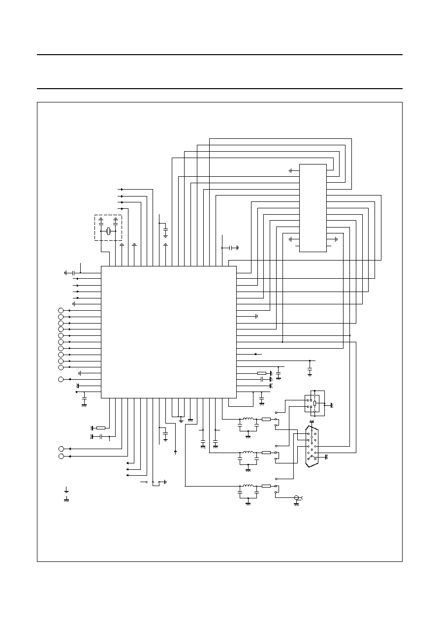
Fig.19 SAA8110G system configuration for camera application (continued from Fig.18).
handbook, full pagewidth
MGK394
1
3
5
7
9
11
13
15
17
19
2
4
6
8
10
SAA8110G
DIGITAL SIGNAL PROCESSOR
12
14
16
18
20
10 nF
100 nF
100
nF
100 nF
100 nF
100 nF
SMP_CLK (to power supply)
P0
digital ground
analog ground
P1
RESET_DSP
(from
µ
C)
21
VDDA2
VDDA3
VDDA3
VDDA3
VDDA3
22 23 24 25 26 27 28 29 30 31 32 33 34 35 36 37
68
68
68
47 k
150 k
38 39 40
80 79
100 nF
A1/SN
RES
A0/SN
DA
SDA
optional
SCL/SN
CL
78 77 76 75 74 73 72 71 70 69 68 67 66 65 64 63 62 61
60
58
56
54
52
50
48
46
44
42
59
57
55
53
51
49
47
45
43
41
CVBS-RCA
CVBS
V, Red
U, Blue
C
Green
Y
SVHS
3
4
1
2
3
4
5
11
12
13
14
15
6
7
8
9
10
1
2
6
7
5
VDDD(C1)
VSYNCIN
VD
FIIN
FI
CCD9
CCD7
CCD5
CCD3
CCD1
VSSD(C2)
VDDD
VDDD
VSSA(CD)
CLK1
CLK1
HSYNCIN
HD
VSSD(C1)
VDDD
CCD8
CCD6
CCD4
CCD2
CCD0
SCLK
CDAC
RBIAS
V
DDA(CD)
S
D
ATA
STROBE
SMP
P0
P1
SIS
V
DDD(C2)
RESET
T2
T1
T0
V
SSA(OB)
OUT3
V
DDA(O3)
OUT2
V
DDA(O2)
OUT1
V
DDA(O1)
CDACOUT
CDAC
OUT
UV1
100 nF
100
nF
UV7
LLC
HREF
FIOUT
VDDD(P1)
RBIAS
VSSA(BG)
UV2
UV3
UV4
UV5
UV6
VSSD(P1)
V
DDD(P2)
VDDD
VDDD
CREF/PXQ
VSYNCOUT
CLK2
CLK2 (from PPG)
VDDA(BG)
DECOUPL
100 nF
100 nF
100 nF
VDDA(DC)
X
OUT
A0/SN
DA
V
DDD(C3)
Y0
Y2
Y4
Y6
X
IN
V
SSD(C4)
SCL/SN
CL
V
SSD(C3)
SDA
A1/SN
RES
V
SSD(P2)
Y1
Y3
Y5
Y7
UV0
VDDD
VDDD
VDDD
26
24
22
20
18
16
DIGIT
AL OUTPUT CONNECT
OR
14
12
10
8
6
4
2
25
23
21
19
17
15
13
11
9
7
5
3
1
L
(1)
L
(1)
L
(1)
L
(1)
L
(1)
L
(1)
L
(1)
L
(1)
L
(1)
A
B
C
D
E
F
G
H
I
J
K
L
M
(1) Values depend on DSP output configuration.

1997 Jun 13
30
Philips Semiconductors
Preliminary specification
Digital Signal Processor (DSP) for
cameras
SAA8110G
PACKAGE OUTLINE
UNIT
A
max.
A
1
A
2
A
3
b
p
c
E
(1)
e
H
E
L
L
p
Q
Z
y
w
v
REFERENCES
OUTLINE
VERSION
EUROPEAN
PROJECTION
ISSUE DATE
IEC
JEDEC
EIAJ
mm
1.6
0.16
0.04
1.5
1.3
0.25
0.25
0.13
0.18
0.12
12.1
11.9
0.5
14.15
13.85
0.70
0.58
1.45
1.05
4
0
o
o
0.15
0.1
0.2
1.0
DIMENSIONS (mm are the original dimensions)
Note
1. Plastic or metal protrusions of 0.25 mm maximum per side are not included.
0.7
0.3
SOT315-1
92-03-24
95-12-19
D
(1)
(1)
(1)
12.1
11.9
H
D
14.15
13.85
E
Z
1.45
1.05
D
b
p
e
E
A
1
A
L
p
Q
detail X
L
(A )
3
B
20
c
D
H
b
p
E
H
A
2
v
M
B
D
Z D
A
Z E
e
v
M
A
X
1
80
61
60
41
40
21
y
pin 1 index
w
M
w
M
0
5
10 mm
scale
LQFP80: plastic low profile quad flat package; 80 leads; body 12 x 12 x 1.4 mm
SOT315-1

1997 Jun 13
31
Philips Semiconductors
Preliminary specification
Digital Signal Processor (DSP) for
cameras
SAA8110G
SOLDERING
Introduction
There is no soldering method that is ideal for all IC
packages. Wave soldering is often preferred when
through-hole and surface mounted components are mixed
on one printed-circuit board. However, wave soldering is
not always suitable for surface mounted ICs, or for
printed-circuits with high population densities. In these
situations reflow soldering is often used.
This text gives a very brief insight to a complex technology.
A more in-depth account of soldering ICs can be found in
our
"IC Package Databook" (order code 9398 652 90011).
Reflow soldering
Reflow soldering techniques are suitable for all LQFP
packages.
Reflow soldering requires solder paste (a suspension of
fine solder particles, flux and binding agent) to be applied
to the printed-circuit board by screen printing, stencilling or
pressure-syringe dispensing before package placement.
Several techniques exist for reflowing; for example,
thermal conduction by heated belt. Dwell times vary
between 50 and 300 seconds depending on heating
method. Typical reflow temperatures range from
215 to 250
∞
C.
Preheating is necessary to dry the paste and evaporate
the binding agent. Preheating duration: 45 minutes at
45
∞
C.
Wave soldering
Wave soldering is not recommended for LQFP packages.
This is because of the likelihood of solder bridging due to
closely-spaced leads and the possibility of incomplete
solder penetration in multi-lead devices.
If wave soldering cannot be avoided, the following
conditions must be observed:
∑
A double-wave (a turbulent wave with high upward
pressure followed by a smooth laminar wave)
soldering technique should be used.
∑
The footprint must be at an angle of 45
∞
to the board
direction and must incorporate solder thieves
downstream and at the side corners.
Even with these conditions, do not consider wave
soldering LQFP packages LQFP48 (SOT313-2),
LQFP64 (SOT314-2) or LQFP80 (SOT315-1).
During placement and before soldering, the package must
be fixed with a droplet of adhesive. The adhesive can be
applied by screen printing, pin transfer or syringe
dispensing. The package can be soldered after the
adhesive is cured.
Maximum permissible solder temperature is 260
∞
C, and
maximum duration of package immersion in solder is
10 seconds, if cooled to less than 150
∞
C within
6 seconds. Typical dwell time is 4 seconds at 250
∞
C.
A mildly-activated flux will eliminate the need for removal
of corrosive residues in most applications.
Repairing soldered joints
Fix the component by first soldering two diagonally-
opposite end leads. Use only a low voltage soldering iron
(less than 24 V) applied to the flat part of the lead. Contact
time must be limited to 10 seconds at up to 300
∞
C. When
using a dedicated tool, all other leads can be soldered in
one operation within 2 to 5 seconds between
270 and 320
∞
C.

1997 Jun 13
32
Philips Semiconductors
Preliminary specification
Digital Signal Processor (DSP) for
cameras
SAA8110G
DEFINITIONS
LIFE SUPPORT APPLICATIONS
These products are not designed for use in life support appliances, devices, or systems where malfunction of these
products can reasonably be expected to result in personal injury. Philips customers using or selling these products for
use in such applications do so at their own risk and agree to fully indemnify Philips for any damages resulting from such
improper use or sale.
PURCHASE OF PHILIPS I
2
C COMPONENTS
Data sheet status
Objective specification
This data sheet contains target or goal specifications for product development.
Preliminary specification
This data sheet contains preliminary data; supplementary data may be published later.
Product specification
This data sheet contains final product specifications.
Limiting values
Limiting values given are in accordance with the Absolute Maximum Rating System (IEC 134). Stress above one or
more of the limiting values may cause permanent damage to the device. These are stress ratings only and operation
of the device at these or at any other conditions above those given in the Characteristics sections of the specification
is not implied. Exposure to limiting values for extended periods may affect device reliability.
Application information
Where application information is given, it is advisory and does not form part of the specification.
Purchase of Philips I
2
C components conveys a license under the Philips' I
2
C patent to use the
components in the I
2
C system provided the system conforms to the I
2
C specification defined by
Philips. This specification can be ordered using the code 9398 393 40011.

1997 Jun 13
33
Philips Semiconductors
Preliminary specification
Digital Signal Processor (DSP) for
cameras
SAA8110G
NOTES

1997 Jun 13
34
Philips Semiconductors
Preliminary specification
Digital Signal Processor (DSP) for
cameras
SAA8110G
NOTES

1997 Jun 13
35
Philips Semiconductors
Preliminary specification
Digital Signal Processor (DSP) for
cameras
SAA8110G
NOTES

Internet: http://www.semiconductors.philips.com
Philips Semiconductors ≠ a worldwide company
© Philips Electronics N.V. 1997
SCA54
All rights are reserved. Reproduction in whole or in part is prohibited without the prior written consent of the copyright owner.
The information presented in this document does not form part of any quotation or contract, is believed to be accurate and reliable and may be changed
without notice. No liability will be accepted by the publisher for any consequence of its use. Publication thereof does not convey nor imply any license
under patent- or other industrial or intellectual property rights.
Netherlands: Postbus 90050, 5600 PB EINDHOVEN, Bldg. VB,
Tel. +31 40 27 82785, Fax. +31 40 27 88399
New Zealand: 2 Wagener Place, C.P.O. Box 1041, AUCKLAND,
Tel. +64 9 849 4160, Fax. +64 9 849 7811
Norway: Box 1, Manglerud 0612, OSLO,
Tel. +47 22 74 8000, Fax. +47 22 74 8341
Philippines: Philips Semiconductors Philippines Inc.,
106 Valero St. Salcedo Village, P.O. Box 2108 MCC, MAKATI,
Metro MANILA, Tel. +63 2 816 6380, Fax. +63 2 817 3474
Poland: Ul. Lukiska 10, PL 04-123 WARSZAWA,
Tel. +48 22 612 2831, Fax. +48 22 612 2327
Portugal: see Spain
Romania: see Italy
Russia: Philips Russia, Ul. Usatcheva 35A, 119048 MOSCOW,
Tel. +7 095 755 6918, Fax. +7 095 755 6919
Singapore: Lorong 1, Toa Payoh, SINGAPORE 1231,
Tel. +65 350 2538, Fax. +65 251 6500
Slovakia: see Austria
Slovenia: see Italy
South Africa: S.A. PHILIPS Pty Ltd., 195-215 Main Road Martindale,
2092 JOHANNESBURG, P.O. Box 7430 Johannesburg 2000,
Tel. +27 11 470 5911, Fax. +27 11 470 5494
South America: Rua do Rocio 220, 5th floor, Suite 51,
04552-903 S„o Paulo, S√O PAULO - SP, Brazil,
Tel. +55 11 821 2333, Fax. +55 11 829 1849
Spain: Balmes 22, 08007 BARCELONA,
Tel. +34 3 301 6312, Fax. +34 3 301 4107
Sweden: Kottbygatan 7, Akalla, S-16485 STOCKHOLM,
Tel. +46 8 632 2000, Fax. +46 8 632 2745
Switzerland: Allmendstrasse 140, CH-8027 ZÐRICH,
Tel. +41 1 488 2686, Fax. +41 1 481 7730
Taiwan: Philips Semiconductors, 6F, No. 96, Chien Kuo N. Rd., Sec. 1,
TAIPEI, Taiwan Tel. +886 2 2134 2865, Fax. +886 2 2134 2874
Thailand: PHILIPS ELECTRONICS (THAILAND) Ltd.,
209/2 Sanpavuth-Bangna Road Prakanong, BANGKOK 10260,
Tel. +66 2 745 4090, Fax. +66 2 398 0793
Turkey: Talatpasa Cad. No. 5, 80640 GÐLTEPE/ISTANBUL,
Tel. +90 212 279 2770, Fax. +90 212 282 6707
Ukraine: PHILIPS UKRAINE, 4 Patrice Lumumba str., Building B, Floor 7,
252042 KIEV, Tel. +380 44 264 2776, Fax. +380 44 268 0461
United Kingdom: Philips Semiconductors Ltd., 276 Bath Road, Hayes,
MIDDLESEX UB3 5BX, Tel. +44 181 730 5000, Fax. +44 181 754 8421
United States: 811 East Arques Avenue, SUNNYVALE, CA 94088-3409,
Tel. +1 800 234 7381
Uruguay: see South America
Vietnam: see Singapore
Yugoslavia: PHILIPS, Trg N. Pasica 5/v, 11000 BEOGRAD,
Tel. +381 11 625 344, Fax.+381 11 635 777
For all other countries apply to: Philips Semiconductors, Marketing & Sales Communications,
Building BE-p, P.O. Box 218, 5600 MD EINDHOVEN, The Netherlands, Fax. +31 40 27 24825
Argentina: see South America
Australia: 34 Waterloo Road, NORTH RYDE, NSW 2113,
Tel. +61 2 9805 4455, Fax. +61 2 9805 4466
Austria: Computerstr. 6, A-1101 WIEN, P.O. Box 213,
Tel. +43 1 60 101, Fax. +43 1 60 101 1210
Belarus: Hotel Minsk Business Center, Bld. 3, r. 1211, Volodarski Str. 6,
220050 MINSK, Tel. +375 172 200 733, Fax. +375 172 200 773
Belgium: see The Netherlands
Brazil: see South America
Bulgaria: Philips Bulgaria Ltd., Energoproject, 15th floor,
51 James Bourchier Blvd., 1407 SOFIA,
Tel. +359 2 689 211, Fax. +359 2 689 102
Canada: PHILIPS SEMICONDUCTORS/COMPONENTS,
Tel. +1 800 234 7381
China/Hong Kong: 501 Hong Kong Industrial Technology Centre,
72 Tat Chee Avenue, Kowloon Tong, HONG KONG,
Tel. +852 2319 7888, Fax. +852 2319 7700
Colombia: see South America
Czech Republic: see Austria
Denmark: Prags Boulevard 80, PB 1919, DK-2300 COPENHAGEN S,
Tel. +45 32 88 2636, Fax. +45 31 57 0044
Finland: Sinikalliontie 3, FIN-02630 ESPOO,
Tel. +358 9 615800, Fax. +358 9 61580920
France: 4 Rue du Port-aux-Vins, BP317, 92156 SURESNES Cedex,
Tel. +33 1 40 99 6161, Fax. +33 1 40 99 6427
Germany: Hammerbrookstraþe 69, D-20097 HAMBURG,
Tel. +49 40 23 53 60, Fax. +49 40 23 536 300
Greece: No. 15, 25th March Street, GR 17778 TAVROS/ATHENS,
Tel. +30 1 4894 339/239, Fax. +30 1 4814 240
Hungary: see Austria
India: Philips INDIA Ltd, Shivsagar Estate, A Block, Dr. Annie Besant Rd.
Worli, MUMBAI 400 018, Tel. +91 22 4938 541, Fax. +91 22 4938 722
Indonesia: see Singapore
Ireland: Newstead, Clonskeagh, DUBLIN 14,
Tel. +353 1 7640 000, Fax. +353 1 7640 200
Israel: RAPAC Electronics, 7 Kehilat Saloniki St, PO Box 18053,
TEL AVIV 61180, Tel. +972 3 645 0444, Fax. +972 3 649 1007
Italy: PHILIPS SEMICONDUCTORS, Piazza IV Novembre 3,
20124 MILANO, Tel. +39 2 6752 2531, Fax. +39 2 6752 2557
Japan: Philips Bldg 13-37, Kohnan 2-chome, Minato-ku, TOKYO 108,
Tel. +81 3 3740 5130, Fax. +81 3 3740 5077
Korea: Philips House, 260-199 Itaewon-dong, Yongsan-ku, SEOUL,
Tel. +82 2 709 1412, Fax. +82 2 709 1415
Malaysia: No. 76 Jalan Universiti, 46200 PETALING JAYA, SELANGOR,
Tel. +60 3 750 5214, Fax. +60 3 757 4880
Mexico: 5900 Gateway East, Suite 200, EL PASO, TEXAS 79905,
Tel. +9-5 800 234 7381
Middle East: see Italy
Printed in The Netherlands
547047/1200/01/pp36
Date of release: 1997 Jun 13
Document order number:
9397 750 01576