Document Outline
- 1 FEATURES
- 2 APPLICATIONS
- 3 GENERAL DESCRIPTION
- ORDERING INFORMATION
- 5 QUICK REFERENCE DATA
- 6 BLOCK DIAGRAM
- 7 PINNING
- 8 FUNCTIONAL DESCRIPTION
- 8.1 Black offset preprocessing
- 8.2 Y, CR and CB separation
- 8.3 RGB processing
- 8.4 Y processing
- 8.5 RGB to UV conversion
- 8.6 UV processing
- 8.7 Display function
- 8.8 Analog output processing
- 8.9 Measurement engine
- 8.10 VH reference and window timing and control
- 8.11 Pulse pattern generator
- 8.12 Miscellaneous functions
- 8.13 Mode control
- 8.14 Microcontroller
- 8.15 Audio amplifier
- 8.16 I 2 C-bus interface
- 9 LIMITING VALUES
- 10 THERMAL CHARACTERISTICS
- 11 OPERATING CHARACTERISTICS
- 12 ELECTRICAL CHARACTERISTICS
- 13 APPLICATION INFORMATION
- 14 PACKAGE OUTLINE
- 15 SOLDERING
- 16 DEFINITIONS
- 17 LIFE SUPPORT APPLICATIONS
- 18 PURCHASE OF PHILIPS I 2 C COMPONENTS

DATA SHEET
Preliminary specification
File under Integrated Circuits, IC22
1999 Sep 27
INTEGRATED CIRCUITS
SAA8113HL
Digital PC-camera signal processor

1999 Sep 27
2
Philips Semiconductors
Preliminary specification
Digital PC-camera signal processor
SAA8113HL
CONTENTS
1
FEATURES
2
APPLICATIONS
3
GENERAL DESCRIPTION
4
ORDERING INFORMATION
5
QUICK REFERENCE DATA
6
BLOCK DIAGRAM
7
PINNING
8
FUNCTIONAL DESCRIPTION
8.1
Black offset preprocessing
8.2
Y, C
R
and C
B
separation
8.3
RGB processing
8.4
Y processing
8.5
RGB to UV conversion
8.6
UV processing
8.7
Display function
8.8
Analog output processing
8.9
Measurement engine
8.10
VH reference and window timing and control
8.11
Pulse pattern generator
8.12
Miscellaneous functions
8.13
Mode control
8.14
Microcontroller
8.15
Audio amplifier
8.16
I
2
C-bus interface
9
LIMITING VALUES
10
THERMAL CHARACTERISTICS
11
OPERATING CHARACTERISTICS
12
ELECTRICAL CHARACTERISTICS
13
APPLICATION INFORMATION
14
PACKAGE OUTLINE
15
SOLDERING
15.1
Introduction to soldering surface mount
packages
15.2
Reflow soldering
15.3
Wave soldering
15.4
Manual soldering
15.5
Suitability of surface mount IC packages for
wave and reflow soldering methods
16
DEFINITIONS
17
LIFE SUPPORT APPLICATIONS
18
PURCHASE OF PHILIPS I
2
C COMPONENTS

1999 Sep 27
3
Philips Semiconductors
Preliminary specification
Digital PC-camera signal processor
SAA8113HL
1
FEATURES
∑
High precision digital processing with 10-bit input
∑
Medium resolution complementary mosaic CCD
sensors PAL or NTSC (interlaced mode only)
∑
Internal PPG, dedicated to SHARP, TOSHIBA and
PANASONIC sensors
∑
Integrated microcontroller (80C51) for control loops
Auto Optical Black (AOB), Auto White Balance (AWB)
and Auto Exposure (AE)
∑
Black offset preprocessing
∑
RGB separation
∑
RGB processing (colour correction matrix,
programmable knee and gamma)
∑
Separate Y-processing (saturation concealment,
programmable knee and gamma)
∑
RGB to UV conversion (including down-sampling filters)
∑
Noise reduction in Y and UV
∑
Display function for system evaluation
∑
Analog output processing, including PAL/NTSC encoder
and 9-bit Video Digital-to-Analog Converter (VDAC)
∑
Measurement engine (prepared for AE and AWB
features)
∑
Miscellaneous functions, e.g. power management, 7-bit
Control DAC (CDAC) serial interface with preprocessing
∑
VH reference and window timing for internal use
∑
Master I
2
C-bus interface for communication with an
external EEPROM (containing the default settings)
∑
Slave I
2
C-bus interface for communication with an
external microcontroller
∑
Parallel interface for communication with an external
EPROM (for ROM code debugging)
∑
Integrated audio amplifier.
2
APPLICATIONS
∑
Low-cost desktop video applications
∑
Videophone systems.
3
GENERAL DESCRIPTION
The SAA8113HL is a 2nd generation camera Digital
Signal Processor (DSP) designed for low-cost DTV
applications. It integrates the DSP core, the Pulse Pattern
Generator (PPG), the 80C51 microcontroller and the
VDAC in one IC. It is the successor of the SAA8110G,
dedicated to analog output cameras.
The SAA8113HL must be applied together with an analog
front-end that includes a Correlated Double Sampling
(CDS), an Automatic Gain Control (AGC) and an
Analog-to-Digital Converter (ADC). This may be the
TDA8786 or the TDA8784.
The PPG generates the timing pulses to drive medium
resolution PAL/NTSC complementary mosaic CCD
sensors (512
◊
492 NTSC and 512
◊
582 PAL).
The input of the DSP is 10 bits with a maximum pixel
frequency equal to 9.66 MHz. The DSP core processes
this sensor signal to a standard video output signal. The
SAA8113HL output is an analog CVBS video signal.
The microcontroller provides the settings for the IC
registers from EEPROM at power-up or reset and controls
the AWB, AE and AOB loops. It also provides a hardware
I
2
C-bus interface, so the microcontroller can be used as an
I
2
C-bus slave. The software code is embedded in an
internal ROM but it is also possible to use a combined data
and address bus, connected to an external program
EPROM.
A built-in power management function allows the power
dissipation to be optimized.
4
ORDERING INFORMATION
TYPE
NUMBER
PACKAGE
NAME
DESCRIPTION
VERSION
SAA8113HL
LQFP100
plastic low profile quad flat package; 100 leads;
body 14
◊
14
◊
1.4 mm
SOT407-1

1999 Sep 27
4
Philips Semiconductors
Preliminary specification
Digital PC-camera signal processor
SAA8113HL
5
QUICK REFERENCE DATA
Measured over full voltage and temperature range.
Note
1. This concerns pins SCL and SDA.
SYMBOL
PARAMETER
CONDITIONS
MIN.
TYP.
MAX.
UNIT
V
DDD
digital supply voltage
3.0
3.3
3.6
V
V
DDA
analog supply voltage
3.0
3.3
3.6
V
I
DD(tot)
total supply current
V
DDD
= 3.3 V
-
60
-
mA
V
I
input voltage
3.0 V < V
DDD
< 3.6 V
low-voltage TTL compatible
V
note 1
5 V tolerant, TTL compatible
V
V
O
output voltage
3.0 V < V
DDD
< 3.6 V
low-voltage TTL compatible
V
note 1
5 V tolerant, TTL compatible
V
f
clk
clock frequency input
-
38
-
MHz
duty factor of f
clk
-
50
-
%
P
tot
total power dissipation
T
amb
= 25
∞
C
-
200
250
mW
T
stg
storage temperature
-
55
-
+150
∞
C
T
amb
ambient temperature
0
25
70
∞
C
T
j
junction temperature
T
amb
= 70
∞
C
-
40
-
+125
∞
C

1999
Sep
27
5
Philips Semiconductors
Preliminar
y specification
Digital PC-camer
a signal processor
SAA8113HL
This text is here in white to force landscape pages to be rotated correctly when browsing through the pdf in the Acrobat reader.This text is here in
_
white to force landscape pages to be rotated correctly when browsing through the pdf in the Acrobat reader.This text is here inThis text is here in
white to force landscape pages to be rotated correctly when browsing through the pdf in the Acrobat reader. white to force landscape pages to be ...
6
BLOCK DIA
GRAM
b
ook, full pagewidth
FCE312
MICRO-
CONTROLLER
80C51
SAA8113HL
INTERNAL
MICRO-
CONTROLLER
INTERFACE
ANALOG
OUTPUT
(PRE-
PROCESSING)
PAL/NTSC
ENCODER
P1
P2
AUDIO BUFFER
VDAC
P0
P4
P3
5, 6, 7, 8
11
SDAE
15
SDA
14
SCL
DISPLAY
UV
PROCESSING
RGB
TO
UV
RGB
PROCESSING
Y
AND
CR, CB
SEPARATION
OFFSET
PRE-
PROCESSING
Y
PROCESSING
10
SCLE
85 to 94
MODE
CONTROL
AND
CLOCK
GENERATOR
1 to 3
2
8
3
9
2
2
8
7
4
2
4
6
3
8
3
10
62
63
59
58
50
ALE
49 to 42
P0.7 to P0.0
39 to 33
AD14 to AD8
KNOB3
to
KNOB0
CCD9
to
CCD0
M2 to M0
32
PSEN
22
18
27
26, 28
29
VDDA4
24, 25
55, 96
VDDD1,
VDDD2
13, 17, 23,
40, 57, 64, 71, 83
54, 56, 95
12, 19, 20, 21,
41, 60, 61, 72, 82
AGND5,
AGND6
MICIAB,
VCOMAB
VDDA1 to VDDA3,
VDDA5 to VDDA9
DGND1 to DGND3
AGND1 to AGND4,
AGND7 to AGND11
OUTAB
XOSC
XIN
XOUT
CDACOUT
RBIASCDAC
MISCELLANEOUS
FUNCTIONS
PPG
SENSOR/PREPROCESSOR TIMING AND CONTROL
VH
REFERENCE
TIMING
MEASUREMENT ENGINE
CDAC
4
16, 53
KNOB4
9
RESET
52
EA
100, 99,
98, 97,
84, 51,
30, 31
SDATA,
SCLK,
STROBE,
STDBY,
SMP,
LED,
OUTBVEN,
OUTGAIN
65, 66,
67, 68,
69, 70
V1X,
VH1X,
V2X,
V3X,
VH3X,
V4X
75,
74, 76
FH1,
FH2,
FR
73
OFDX
79, 80,
77, 78
BCP,
DCP,
FS,
FCDS
81
T1,
INT1
CLK1
VDOBCVBS
DECREF
Fig.1 Block diagram.

1999 Sep 27
6
Philips Semiconductors
Preliminary specification
Digital PC-camera signal processor
SAA8113HL
7
PINNING
SYMBOL
PIN
I/O
DESCRIPTION
M2
1
I
test mode control signal bit 2
M1
2
I
test mode control signal bit 1
M0
3
I
test mode control signal bit 0
KNOB4
4
I
input connected to DSP core
KNOB3
5
I/O
I/O connected to internal 80C51
KNOB2
6
I/O
I/O connected to internal 80C51
KNOB1
7
I/O
I/O connected to internal 80C51
KNOB0
8
I/O
I/O connected to internal 80C51
RESET
9
I
Power-on reset
SCLE
10
O
master I
2
C-bus clock output to control EEPROM
SDAE
11
I/O
master I
2
C-bus data I/O to control EEPROM
AGND1
12
I
analog ground 1 for output buffers
V
DDA1
13
I
analog supply voltage 1 for output buffers
SCL
14
I
slave I
2
C-bus clock input
SDA
15
I/O
slave I
2
C-bus data I/O
T1
16
I
Timer 1 for internal 80C51
V
DDA2
17
I
analog supply voltage 2 for DAC output buffer
VDOBCVBS
18
O
VDAC output buffer for CVBS signal
AGND2
19
I
analog ground 2 for DAC output buffer
AGND3
20
I
analog ground 3 for analog DAC core and band gap (connected to substrate)
AGND4
21
I
analog ground 4 for analog DAC core and band gap (not connected to substrate)
DECREF
22
O
decoupled pin for reference voltage HIGH
V
DDA3
23
I
analog supply voltage 3 for analog DAC core and band gap
MICIAB
24
I
microphone input audio buffer
V
COMAB
25
I
common voltage for audio buffer
AGND5
26
I
analog ground 5 for audio buffer (not connected to substrate)
OUTAB
27
O
output audio buffer
AGND6
28
I
analog ground 6 for audio buffer (connected to substrate)
V
DDA4
29
I
analog supply voltage 4 for audio buffer
OUTBVEN
30
O
output to enable the bias voltage of the microphone for the audio buffer
OUTGAIN
31
O
output to control the gain factor of an external audio buffer
PSEN
32
O
program store enable; read strobe for external program memory (active LOW)
AD8
33
O
address bit 8 for external program memory (PROM)
AD9
34
O
address bit 9 for external program memory (PROM)
AD10
35
O
address bit 10 for external program memory (PROM)
AD11
36
O
address bit 11 for external program memory (PROM)
AD12
37
O
address bit 12 for external program memory (PROM)
AD13
38
O
address bit 13 for external program memory (PROM)
AD14
39
O
address bit 14 for external program memory (PROM)
V
DDA5
40
I
analog supply voltage 5 for output buffers

1999 Sep 27
7
Philips Semiconductors
Preliminary specification
Digital PC-camera signal processor
SAA8113HL
AGND7
41
I
analog ground 7 for output buffers
P0.0
42
I/O
port 0 bidirectional bit 0 for external program memory data I/O (PROM)
P0.1
43
I/O
port 0 bidirectional bit 1 for external program memory data I/O (PROM)
P0.2
44
I/O
port 0 bidirectional bit 2 for external program memory data I/O (PROM)
P0.3
45
I/O
port 0 bidirectional bit 3 for external program memory data I/O (PROM)
P0.4
46
I/O
port 0 bidirectional bit 4 for external program memory data I/O (PROM)
P0.5
47
I/O
port 0 bidirectional bit 5 for external program memory data I/O (PROM)
P0.6
48
I/O
port 0 bidirectional bit 6 for external program memory data I/O (PROM)
P0.7
49
I/O
port 0 bidirectional bit 7 for external program memory data I/O (PROM)
ALE
50
O
address latch enable pulse for external latch
LED
51
O
output to drive LED
EA
52
I
external access select bit for internal 80C51 (active LOW)
INT1
53
I
interrupt 1 for internal 80C51
DGND1
54
I
digital ground 1 for input buffers, predrivers and the digital core
V
DDD1
55
I
digital supply voltage 1 for input buffers, predrivers and the digital core
DGND2
56
I
digital ground 2 for input buffers, predrivers and the digital core
V
DDA6
57
I
analog supply voltage 6 for CDAC
RBIASCDAC
58
O
bias resistor for CDAC
CDACOUT
59
O
output CDAC
AGND8
60
I
analog ground 8 for CDAC
AGND9
61
I
analog ground 9 for 38 MHz (fundamental) crystal oscillator
XIN
62
I
oscillator input
XOUT
63
O
oscillator output
V
DDA7
64
I
analog supply voltage 7 for 38 MHz (fundamental) crystal oscillator
V1X
65
O
vertical CCD transfer pulse 1X
VH1X
66
O
vertical CCD load pulse H1X
V2X
67
O
vertical CCD transfer pulse 2X
V3X
68
O
vertical CCD transfer pulse 3X
VH3X
69
O
vertical CCD load pulse H3X
V4X
70
O
vertical CCD transfer pulse 4X
V
DDA8
71
I
analog supply voltage 8 for output buffers
AGND10
72
I
analog ground 10 for output buffers
OFDX
73
O
overflow drain pulse for shutter control
FH2
74
O
horizontal CCD transfer pulse F2
FH1
75
O
horizontal CCD transfer pulse F1
FR
76
O
CCD output amplifier reset pulse (TDA8786 or TDA8784)
FS
77
O
CCD output level sample and hold pulse (TDA8786 or TDA8784)
FCDS
78
O
reference level sample and hold pulse (TDA8786 or TDA8784)
BCP
79
O
black pixel clamp pulse (TDA8786 or TDA8784)
DCP
80
O
dummy pixel clamp pulse (TDA8786 or TDA8784)
CLK1
81
O
pixel clock to preprocessor (TDA8786 or TDA8784)
SYMBOL
PIN
I/O
DESCRIPTION

1999 Sep 27
8
Philips Semiconductors
Preliminary specification
Digital PC-camera signal processor
SAA8113HL
AGND11
82
I
analog ground 11 for output buffers
V
DDA9
83
I
analog supply voltage 9 for output buffers
SMP
84
O
switch mode pulse for DC-to-DC power supply
CCD9
85
I
(preprocessed) AD-converted CCD signal bit 9
CCD8
86
I
(preprocessed) AD-converted CCD signal bit 8
CCD7
87
I
(preprocessed) AD-converted CCD signal bit 7
CCD6
88
I
(preprocessed) AD-converted CCD signal bit 6
CCD5
89
I
(preprocessed) AD-converted CCD signal bit 5
CCD4
90
I
(preprocessed) AD-converted CCD signal bit 4
CCD3
91
I
(preprocessed) AD-converted CCD signal bit 3
CCD2
92
I
(preprocessed) AD-converted CCD signal bit 2
CCD1
93
I
(preprocessed) AD-converted CCD signal bit 1
CCD0
94
I
(preprocessed) AD-converted CCD signal bit 0
DGND3
95
I
digital ground 3 for input buffers, predrivers and the digital core
V
DDD2
96
I
digital supply voltage 2 for input buffers, predrivers and the digital core
STDBY
97
O
standby control output to TDA8786 or TDA8784
STROBE
98
O
strobe to TDA8786 or TDA8784
SCLK
99
O
serial clock to TDA8786 or TDA8784
SDATA
100
O
serial data to TDA8786 or TDA8784
SYMBOL
PIN
I/O
DESCRIPTION
1999 Sep 27
9
Philips Semiconductors
Preliminary specification
Digital PC-camera signal processor
SAA8113HL
handbook, full pagewidth
75
74
73
72
71
70
69
68
67
66
65
64
63
62
61
60
59
58
57
56
55
54
53
52
51
80
79
78
77
76
DCP
BCP
FCDS
FS
FR
FH1
FH2
OFDX
AGND10
VDDA8
V4X
VH3X
V3X
V2X
VH1X
V1X
VDDA7
XOUT
XIN
AGND9
AGND8
CDACOUT
RBIASCDAC
VDDA6
DGND2
VDDD1
DGND1
INT1
EA
LED
M2
M1
M0
KNOB4
KNOB3
KNOB2
KNOB1
KNOB0
RESET
SCLE
SDAE
AGND1
VDDA1
SCL
SDA
T1
VDDA2
VDOBCVBS
AGND2
AGND3
AGND4
DECREF
VDDA3
MICIAB
VCOMAB
SDATA
SCLK
STROBE
STDBY
V
DDD2
DGND3
CCD0
CCD1
CCD2
CCD3
CCD4
CCD5
CCD6
CCD7
CCD8
CCD9
SMP
V
DDA9
AGND11
CLK1
OUTGAIN
AD8
AD9
AD10
AD11
AD12
AD13
AD14
V
DDA5
AGND7
P0.0
P0.1
P0.2
P0.3
P0.4
P0.5
P0.6
P0.7
ALE
AGND5
OUTAB
AGND6
V
DDA4
OUTBVEN
30
29
28
27
26
25
24
23
22
21
20
19
18
17
16
15
14
13
12
11
10
9
8
7
6
5
4
3
2
1
100
99
98
97
96
95
94
93
92
91
90
89
88
87
86
85
84
83
82
81
31
32
33
34
35
36
37
38
39
40
41
42
43
44
45
46
47
48
49
50
SAA8113HL
PSEN
FCE313
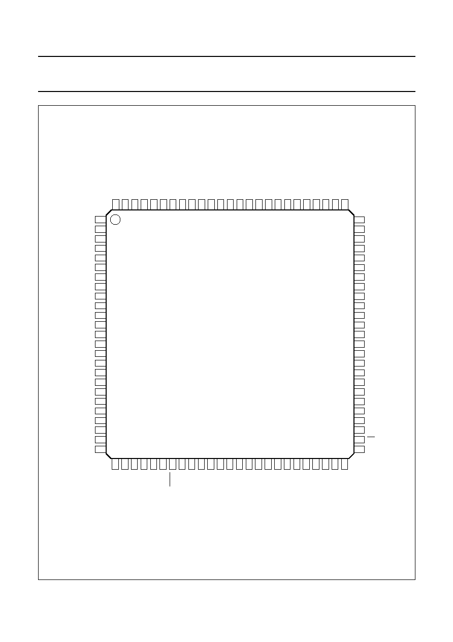
Fig.2 Pin configuration.
1999 Sep 27
10
Philips Semiconductors
Preliminary specification
Digital PC-camera signal processor
SAA8113HL
8
FUNCTIONAL DESCRIPTION
8.1
Black offset preprocessing
The CCD signal contains additional pixels outside the
active window, which are used to measure the reference
black level. These pixels are located in the optical black
window, whose position can be set through the serial
interface. The optical black level can be adjusted by the
microcontroller in order to proceed rapidly. In this case, the
microcontroller directly adjusts the analog preprocessing
clamp included in the TDA8786 or TDA8784 and takes
advantage of the full code range. Otherwise, the black
level is fixed by settings that are downloaded through the
serial interface.
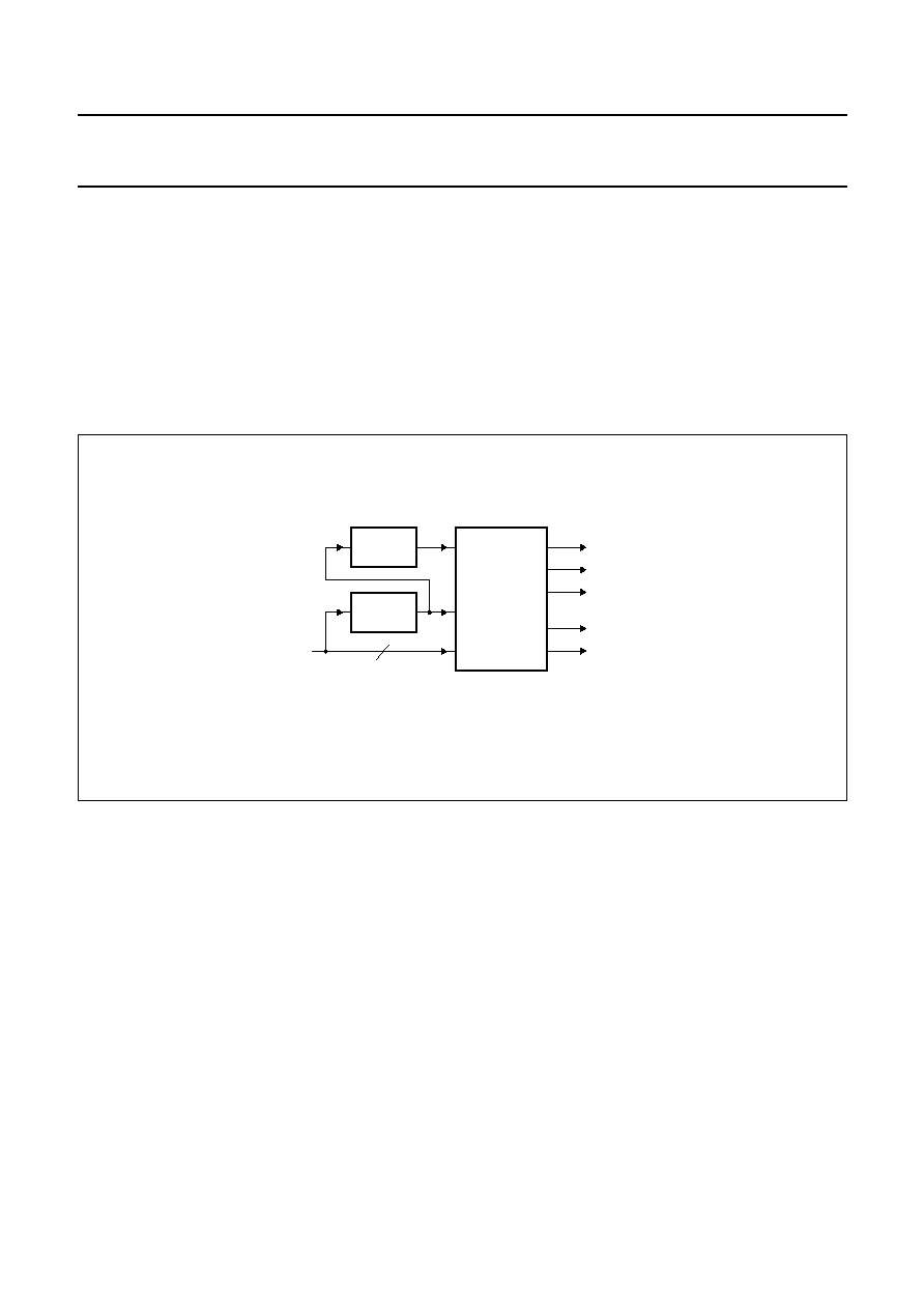
8.2
Y, C
R
and C
B
separation
For each pixel value, this block (see Fig.3) generates the
three components: the luminance signal Y and the two
colour signals C
R
(2R
-
G) and C
B
(2B
-
G). Two line
memories are required for this function. This block also
provides vertical contour and white clip information.
handbook, full pagewidth
FCE314
10
CCD inputs
Y
CR
CB
white clip
Yvertical contour
LINE
MEMORY
LINE
MEMORY
RGB
COLOUR
SEPARATION
Fig.3 Y, C
R
and C
B
separation diagram.
1999 Sep 27
11
Philips Semiconductors
Preliminary specification
Digital PC-camera signal processor
SAA8113HL
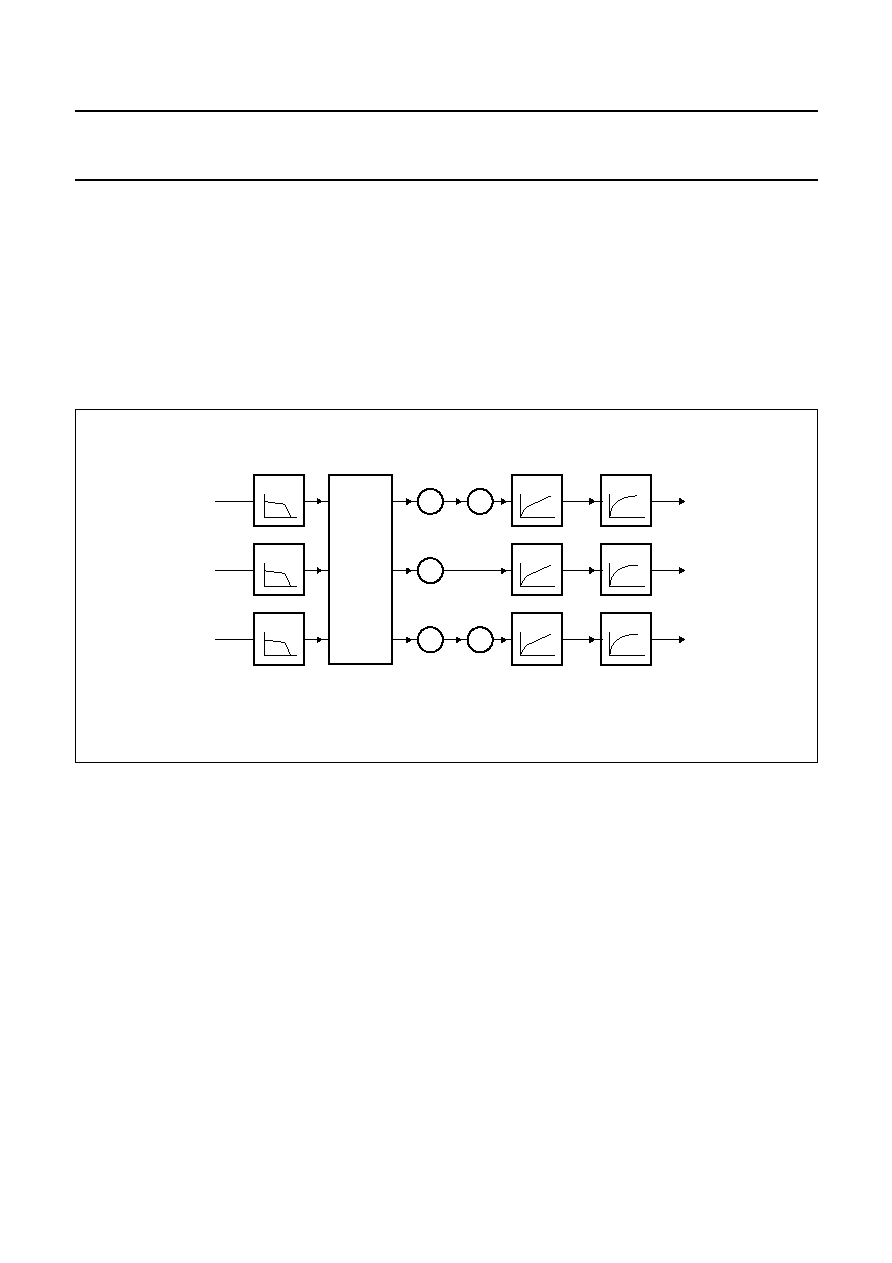
8.3
RGB processing
The RGB processing (see Fig.4) includes several features:
∑
Colour space matrix to handle different types of colour
sensors. The result is an optimum colour reproduction
through the minimization of colour errors. The default
matrix coefficients (positive or negative) can be adjusted
through an external interface.
∑
Separate and adjustable black offsets for
R, G and B signals.
∑
Separate gain controls for R and B signals dedicated to
white balance control. The colour temperature can be
adjusted independently of the colour matrix.
∑
Knee function (compression factor and knee point are
adjustable).
∑
Adjustable gamma function to compensate for the
non-linearity of display devices.
The RGB path has a reduced bandwidth (less than
1 MHz), which is required for CVBS output.
handbook, full pagewidth
FCE315
KNEE
Y
R
Rgain
Rblack
LPF
GAMMA
◊
+
KNEE
COLOUR
MATRIX
CR
G
Gblack
LPF
GAMMA
+
KNEE
CB
B
Bgain
Bblack
LPF
GAMMA
◊
+
Fig.4 RGB processing diagram.
1999 Sep 27
12
Philips Semiconductors
Preliminary specification
Digital PC-camera signal processor
SAA8113HL
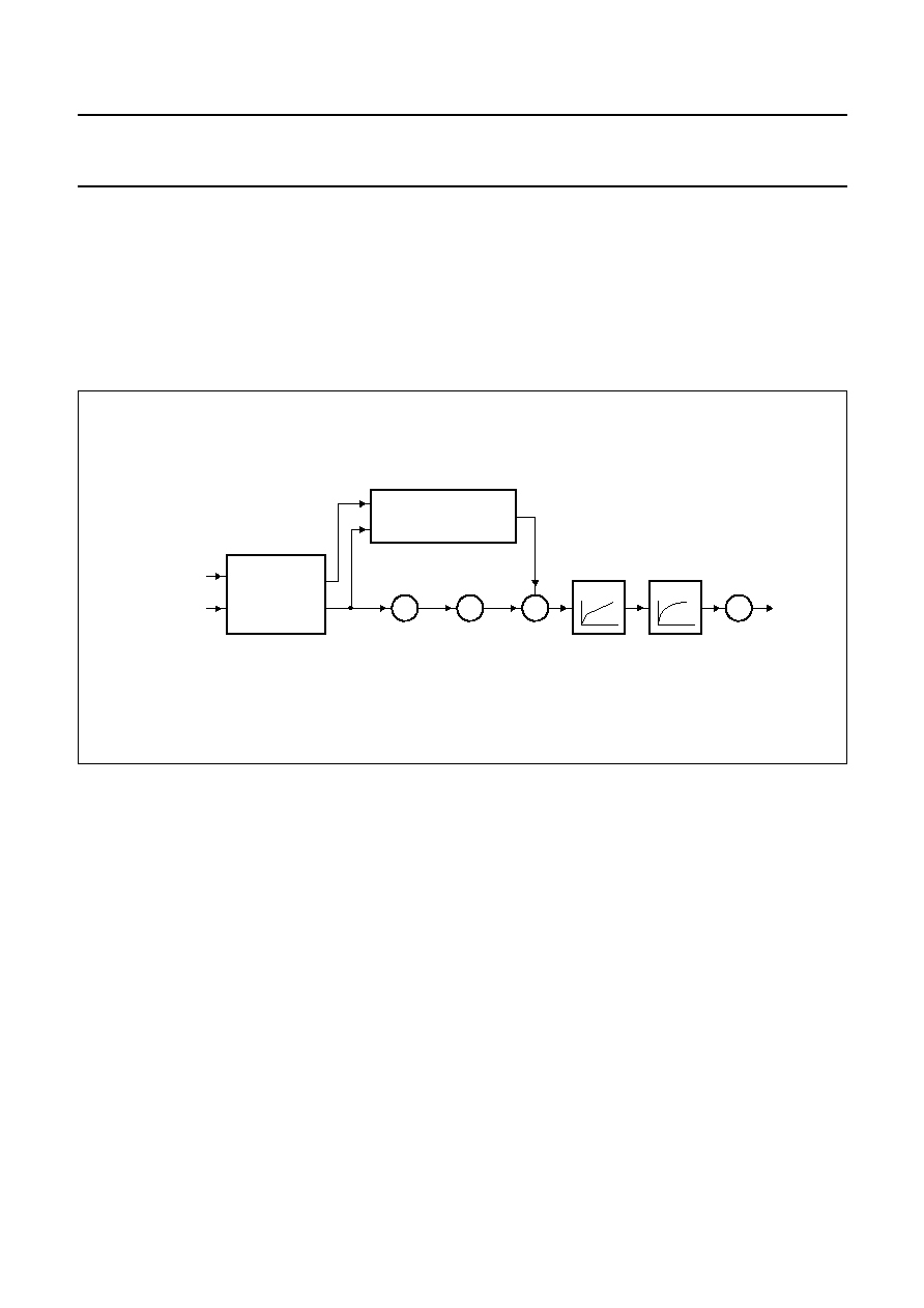
8.4
Y processing
The separate Y processing (see Fig.5) includes the
following features:
∑
Saturation concealment to reduce the typical saturation
distortion
∑
Contour processing to improve picture sharpness
∑
Noise reduction
∑
Black offset
∑
Pre-gain control to adjust the Y signal with respect to the
gamma range
∑
Knee function (compression factor and knee point are
adjustable)
∑
Adjustable gamma function
∑
Gain control.
handbook, full pagewidth
FCE316
KNEE
SATURATION
CONCEALMENT
Y
Y
Ypre-gain
Yblack
Yvertical contour
CONTOUR PROCESSING
AND
NOISE REDUCTION
GAMMA
◊
Ygain
◊
+
+
Fig.5 Y processing diagram.
8.5
RGB to UV conversion
After R, G and B processing, the data path is converted to
U and V signals (see Fig.1). As a result of the reduced
bandwidth, the Y signal is only used as an input for control
loop purposes (measurement engine).
8.6
UV processing
The chrominance processing consists of a noise reduction
by coring and the UV gain control.
8.7
Display function
As an optional feature and for software debugging, it is
possible to visualize:
∑
Eight display bars (assigned via the microcontroller)
∑
Several measurement engine inputs.

1999 Sep 27
13
Philips Semiconductors
Preliminary specification
Digital PC-camera signal processor
SAA8113HL
8.8
Analog output processing
The analog output processing (see Fig.6) contains a
PAL/NTSC encoder to transform the YUV data path to the
CVBS output. The YUV input signals are up-sampled to
twice the pixel clock and digitally prefiltered to keep the
external analog filter simple. The block also contains an
adjustable luminance clipper.
handbook, full pagewidth
FCE317
U
Y
V
sync, blank, scaling, levels
Y
VDOBCVBS
C
PAL/NTSC
ENCODER
MIX
VDAC
Fig.6 Analog output processing.
8.9
Measurement engine
The measurement engine performs data measurements
on a field basis to get inputs for the AE and AWB control
loops of the microcontroller. Up to 16 programmable
windows can be used for the measurement. There are two
down-samplers to prepare the data for two separate
accumulators. It is possible to proceed with eight different
measurements per field (odd and even fields separately).
An internal RAM workspace is used for data handling
operation.
8.10
VH reference and window timing and control
This block generates internal control signals for different
purposes:
∑
Vertical, horizontal and field references (V
D
, H
D
and F
I
)
for PAL or NTSC sensors
∑
Specification of the active window and the optical black
window
∑
Specification of the measurement window grid with
respect to the active window
∑
Specification of the vertical position of the display bars,
see Section 8.7.
All these specifications can be controlled through the serial
interface.

1999 Sep 27
14
Philips Semiconductors
Preliminary specification
Digital PC-camera signal processor
SAA8113HL
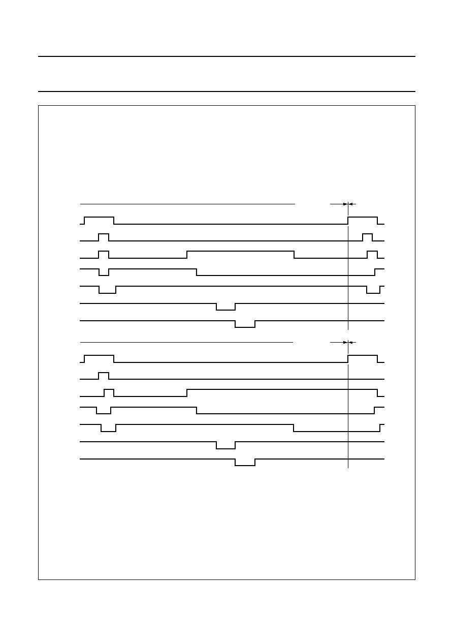
8.11
Pulse pattern generator
The PPG generates timing pulses (Figs. 7 to 10) for
driving the CCD sensor (including the vertical driver) and
pulses for the preprocessor TDA8786 or TDA8784
(correlated double sampling and black clamping).
The PPG is dedicated to the medium resolution sensors
with complementary mosaic colour filters (512
◊
492
NTSC and 512
◊
582 PAL) described in Table 1.
Figs. 11 and 12 show the PPG outputs.
Table 1
Medium resolution CCD sensors driven by the internal PPG; note 1
Note
1. All sensors are used with the vertical driver: NEC
µ
PD16510.
The PPG includes special features:
∑
A charge reset is possible in every active line during the horizontal line blanking and multiple times during the vertical
blanking
∑
A fast shutter interface is available.
BRAND
FORMAT
TYPE
SHARP
PAL 1/4"
LZ2423A
NTSC 1/4"
LZ2413A
PAL 1/5"
LZ2523
NTSC 1/5"
LZ2513
TOSHIBA
PAL 1/4"
TCD5391AP
NTSC 1/4"
TCD5381AP
SHARP low voltage
PAL 1/4"
LZ2425
NTSC 1/4"
LZ2415
PANASONIC
PAL 1/4"
MN37210FP
PAL 1/4"
MN37201FP
NTSC 1/4"
MN37110FP
NTSC 1/4"
MN37101FP

1999 Sep 27
15
Philips Semiconductors
Preliminary specification
Digital PC-camera signal processor
SAA8113HL
handbook, full pagewidth
FCE318
FR_narrow_delayed
FR_wide_delayed
FR_narrow
FR_wide
FS_narrow
FS_wide
FCDS
FH2
FH1
XIN
4
◊
fpixel
delay (typ. 7 ns)
delay (typ. 7 ns)
Fig.7 High speed pulse timing (CCD sensor and preprocessor).
1999 Sep 27
16
Philips Semiconductors
Preliminary specification
Digital PC-camera signal processor
SAA8113HL
handbook, full pagewidth
FCE319
HD
V1X
V2X
V3X
V4X
VH1X
VH3X
NTSC line 18
PAL line 20
NTSC line 17
PAL line 19
HD
V1X
V2X
V3X
V4X
VH1X
VH3X
NTSC line 280
PAL line 332
NTSC line 279
PAL line 331
Fig.8 SHARP and TOSHIBA CCD sensors/vertical drivers.

1999 Sep 27
17
Philips Semiconductors
Preliminary specification
Digital PC-camera signal processor
SAA8113HL
handbook, full pagewidth
FCE320
HD
V1X
V2X
V3X
V4X
VH3X
NTSC line 280
PAL line 332
NTSC line 279
PAL line 331
HD
V1X
V2X
V3X
V4X
VH3X
NTSC line 18
PAL line 20
NTSC line 17
PAL line 19
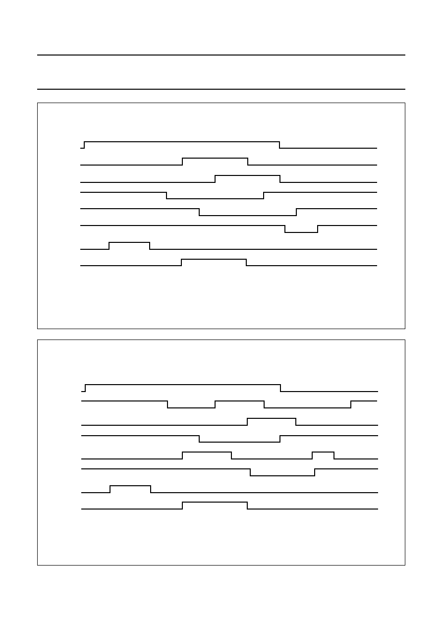
Fig.9 SHARP low-voltage CCD sensors/vertical drivers.

1999 Sep 27
18
Philips Semiconductors
Preliminary specification
Digital PC-camera signal processor
SAA8113HL
handbook, full pagewidth
FCE321
HD
V1X
V2X
V3X
V4X
VH1X
VH3X
OFDX
NTSC line 18
PAL line 20
NTSC line 17
PAL line 19
NTSC line 280
PAL line 332
NTSC line 279
PAL line 331
HD
V1X
V2X
V3X
V4X
VH1X
VH3X
OFDX
Fig.10 PANASONIC CCD sensors/vertical drivers.
1999 Sep 27
19
Philips Semiconductors
Preliminary specification
Digital PC-camera signal processor
SAA8113HL
handbook, full pagewidth
FCE322
HD
V1X
V2X
V3X
V4X
OFDX
BCP
DCP
Fig.11 SHARP, all types, PPG output.
handbook, full pagewidth
FCE323
HD
V1X
V2X
V3X
V4X
OFDX
BCP
DCP
Fig.12 PANASONIC PPG output.
1999 Sep 27
20
Philips Semiconductors
Preliminary specification
Digital PC-camera signal processor
SAA8113HL
8.12
Miscellaneous functions
∑
Power consumption: it is possible to switch the DSP off
without switching off the microcontroller.
∑
Oscillator frequency: a 7-bit CDAC tunes the oscillator
frequency according to the external quartz frequency to
guarantee the typical value of 38 MHz.
The control digital value is downloaded through the
serial interface.
∑
A 3-wire serial bus transfers the settings from the
microcontroller to the preprocessor (TDA8786 or
TDA8784).
8.13
Mode control
This block controls the operational modes of the
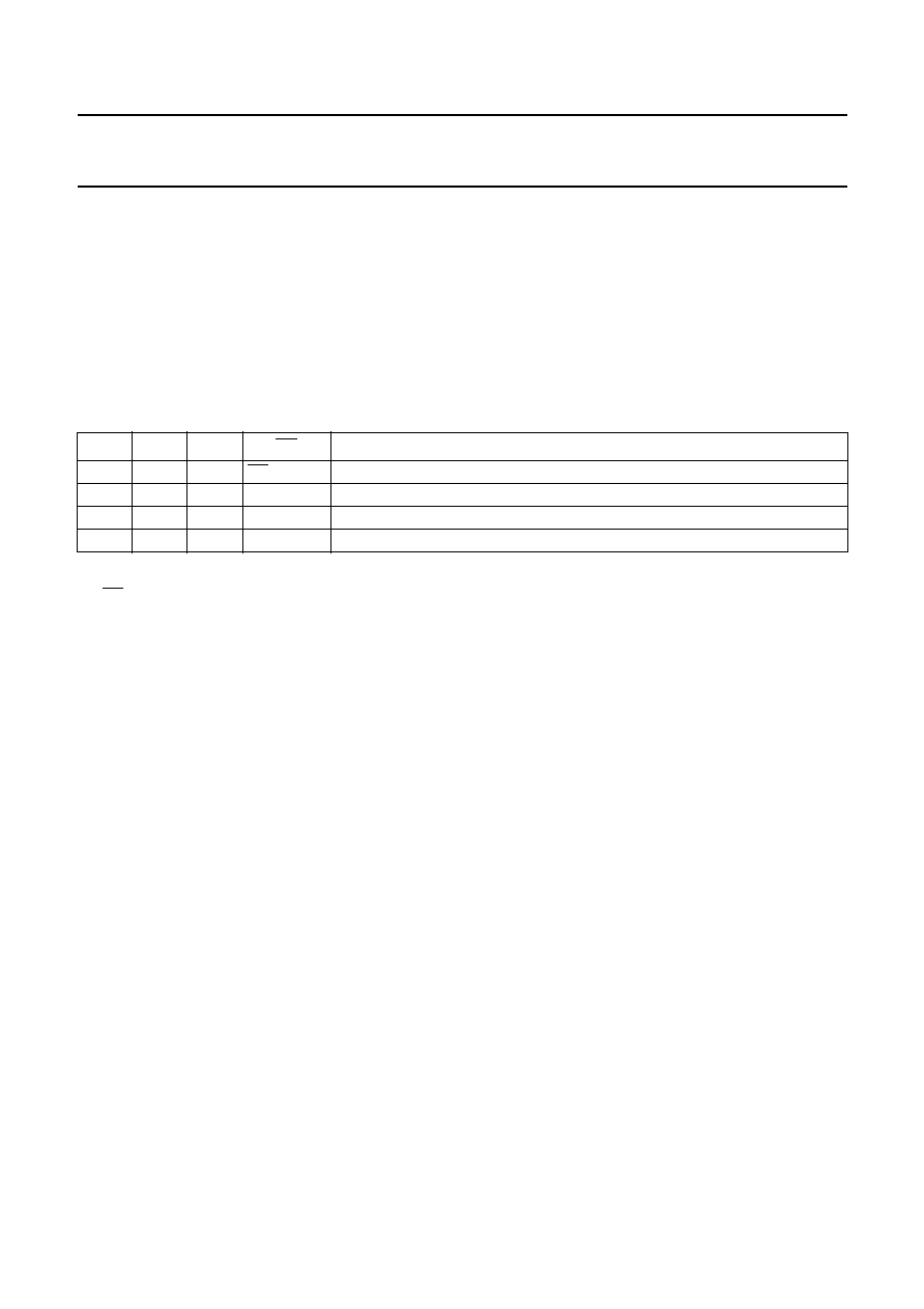
SAA8113HL: application or test modes, see Table 2. For a
smooth adaptability, it is possible to bypass the main
modules.
Table 2
Mode control
Note
1. EA can be high or low, according to the application (high is for internal ROM access, low for external access).
M2
M1
M0
EA
MODE
0
0
0
EA; note 1
application mode
0
0
1
-
application mode with bypassed PPG
0
1
0
-
application mode with bypassed microcontroller
0
1
1
0
application mode with bypassed PPG and microcontroller
8.14
Microcontroller
The embedded microcontroller is basically an 80C654
core (80C51 family) with four ports. Its functionality is
standard, except that the core has no clock divided by 2
and the ports are dedicated input, output or I/O ports.
Ports P0 and P2 are available for connection to a
debugger or to an external program EPROM. The
microcontroller controls the AOB, the AE and the AWB
loops and downloads the settings for the DSP registers
from EEPROM at power-up or reset. Table 3 lists the
80C51 Standard Function Registers.
The microcontroller includes the following features:
∑
16 kbyte internal ROM
∑
256 byte RAM
∑
Hardware I
2
C-bus interface for communication with
external microcontroller: SDA and SCL
∑
Software I
2
C-bus interface for communication with
external EEPROM containing DSP settings: SDAE and
SCLE
∑
Four I/O pins which can be used as human interface
(knobs): P1.0, P1.1, P1.2 and P1.3.

1999 Sep 27
21
Philips Semiconductors
Preliminary specification
Digital PC-camera signal processor
SAA8113HL
Table 3
80C51 Standard Function Registers
SFR
NAME
DESCRIPTION
SFR
ADDRESS
DATA
BIT 7
DATA
BIT 6
DATA
BIT 5
DATA
BIT 4
DATA
BIT 3
DATA
BIT 2
DATA
BIT 1
DATA
BIT 0
B
B register
F0H
B7
B6
B5
B4
B3
B2
B1
B0
ACC
accumulator
E0H
ACC7
ACC6
ACC5
ACC4
ACC3
ACC2
ACC1
ACC0
SIADR
serial interface address
DBH
SA6
SA5
SA4
SA3
SA2
SA1
SA0
GC
SIDAT
serial interface data
DAH
SD7
SD6
SD5
SD4
SD3
SD2
SD1
SD0
SISTA
serial interface status
D9H
ST7
ST6
ST5
ST4
ST3
0
0
0
SICON
serial interface control
D8H
CR2
ENS1
STA
STO
SI
AA
CR1
CR0
PSW
program status word
D0H
CY
AC
F0
RS1
RS0
OV
-
P
P4
port 4
C7H
-
-
-
-
-
-
-
STBY
IP
interrupt priority
B8H
-
IP6
IP5
IP4
PT1
PX1
PT0
PX0
P3
port 3
B0H
RDN
WRN
T1
T0
INT1
INT0
FI
CRST
IE
interrupt enable
A8H
EA
IE6
IE5
IE4
ET1
EX1
ET0
EX0
P2
port 2
A0H
AD15
AD14
AD13
AD12
AD11
AD10
AD9
AD8
P1
port 1
90H
SDA
SCL
SDAE
SCLE
P1.3
P1.2
P1.1
P1.0
TH1
timer HIGH 1
8DH
-
-
-
-
-
-
-
-
TH0
timer HIGH 0
8CH
-
-
-
-
-
-
-
-
TL1
timer LOW 1
8BH
-
-
-
-
-
-
-
-
TL0
timer LOW 0
8AH
-
-
-
-
-
-
-
-
TMOD
timer mode
89H
GATE
C/T
M1
M0
Gate
C/T
M1
M0
TCON
timer control
88H
TF1
TR1
TF0
TR0
IE1
IT1
IE0
IT0
PCON
power control
87H
-
-
-
-
-
-
PD
IDL
DPH
data pointer HIGH
83H
-
-
-
-
-
-
-
-
DPL
data pointer LOW
82H
-
-
-
-
-
-
-
-
SP
stack pointer
81H
SP7
SP6
SP5
SP4
SP3
SP2
SP1
SP0
P0
port 0
80H
AD7
AD6
AD5
AD4
AD3
AD2
AD1
AD0
8.15
Audio amplifier
An analog audio amplifier is integrated in the SAA8113HL.
Its gain can be adjusted between a high (45 dB typical)
and a low (13 dB typical) value through the serial interface.
8.16
I
2
C-bus interface
Table 4 gives the command list of the I
2
C-bus interface.

1999 Sep 27
22
Philips Semiconductors
Preliminary specification
Digital PC-camera signal processor
SAA8113HL
Table 4
Command list
ADD
NAME
FUNCTION
FORMAT
RANGE
0
CONTROL0
see Table 5 for explanation
byte
n.a.
1
CONTROL1
see Table 7 for explanation
byte
n.a.
2
CONTROL2
see Table 8 for explanation
byte
n.a.
3
OB_STARTL_F0
first line optical black window in field 0
byte
[0 to 255]
4
OB_STARTL_F1
first line optical black window in field 1
byte
256 + [0 to 255]
5
OB_STARTP
first pixel optical black window
byte
[0 to 255]
6
OB_PE_F0
fixed optical black level for even pixel in field 0
byte
[0 to 127]
7
OB_PO_F0
fixed optical black level for odd pixel in field 0
byte
[0 to 127]
8
OB_PE_F1
fixed optical black level for even pixel in field 1
byte
[0 to 127]
9
OB_PO_F1
fixed optical black level for odd pixel in field 1
byte
[0 to 127]
10
COL_MAT_P11
colour matrix coefficient p11
byte
[
-
128 to 127]/16
11
COL_MAT_P12
colour matrix coefficient p12
byte
[
-
128 to 127]/16
12
COL_MAT_P13
colour matrix coefficient p13
byte
[
-
128 to 127]/16
13
COL_MAT_P21
colour matrix coefficient p21
byte
[
-
128 to 127]/16
14
COL_MAT_P22
colour matrix coefficient p22
byte
[
-
128 to 127]/16
15
COL_MAT_P23
colour matrix coefficient p23
byte
[
-
128 to 127]/16
16
COL_MAT_P31
colour matrix coefficient p31
byte
[
-
128 to 127]/16
17
COL_MAT_P32
colour matrix coefficient p32
byte
[
-
128 to 127]/16
18
COL_MAT_P33
colour matrix coefficient p33
byte
[
-
128 to 127]/16
19
R_BLACK
fixed R-black level offset
byte
[
-
128 to 127]
20
G_BLACK
fixed G-black level offset
byte
[
-
128 to 127]
21
B_BLACK
fixed B-black level offset
byte
[
-
128 to 127]
22
COL_MAT_RGAIN
colour matrix R-gain factor
byte
[0 to 255]/128
23
COL_MAT_BGAIN
colour matrix B-gain factor
byte
[0 to 255]/64
24
THR_LUM
threshold luminance for fader
byte
[0 to 255]
25
THR_COLOR
threshold colour for fader
byte
[0 to 255]
26
Y_BLACK
fixed Y-black level offset
byte
[
-
128 to 127]
27
K1
gain correction for Y path
byte
[0 to 255]/128
28
RGB_KNEE_OFFSET
offset for RGB knee
byte
[0 to 255]
29
Y_KNEE_OFFSET
offset for Y knee
byte
[0 to 255]
30
RGB_GAMMA_BALANCE
gamma multiplication factor (for RGB data path)
6 bits
[0 to 63]/64
31
Y_GAMMA_BALANCE
gamma multiplication factor (for Y data path)
6 bits
[0 to 63]/64
32
KCOMB
vertical contour comb filter coefficient (MS)
4 bits
[0 to 7]/8
VCGAIN
vertical contour gain (LS)
4 bits
[0 to 15]/16
33
CLDLEV
contour level dependency level
byte
[0 to 255]/2
34
HCLGAIN
horizontal contour BPF low gain (LS)
4 bits
[0 to 15]/16
HCHGAIN
horizontal contour BPF high gain (MS)
4 bits
[0 to 15]/16
35
CNCLEV
contour noise coring level
6 bits
[0 to 63]
36
CONGAIN
contour gain factor; see Table 9
2 bits
[0 to 63]/16
37
VU_VALUE 1
length of VU_Bar 1
byte
2
◊
[0 to 255]

1999 Sep 27
23
Philips Semiconductors
Preliminary specification
Digital PC-camera signal processor
SAA8113HL
38
VU_VALUE 2
length of VU_Bar 2
byte
2
◊
[0 to 255]
39
VU_VALUE 3
length of VU_Bar 3
byte
2
◊
[0 to 255]
40
VU_VALUE 4
length of VU_Bar 4
byte
2
◊
[0 to 255]
41
VU_VALUE 5
length of VU_Bar 5
byte
2
◊
[0 to 255]
42
VU_VALUE 6
length of VU_Bar 6
byte
2
◊
[0 to 255]
43
VU_VALUE 7
length of VU_Bar 7
byte
2
◊
[0 to 255]
44
VU_VALUE 8
length of VU_Bar 8
byte
2
◊
[0 to 255]
45
Y_DISPLAY_OFFSET
display offset (to be used with D_Contour)
byte
4
◊
[0 to 255]
46
UNCLEV
U (chrominance) noise coring level
byte
[0 to 255]/4
47
VNCLEV
V (chrominance) noise coring level
byte
[0 to 255]/4
48
YGAIN
Y (luminance) gain factor
byte
[0 to 255]/128
49
UGAIN
U (B-Y) gain factor
byte
[0 to 255]/128
50
VGAIN
V (R-Y) gain factor
byte
[0 to 255]/128
51
CTR_UPD_LINE
number of line for DB-update control registers
byte
[0 to 255]
52
BURST_LEVEL
burst level colour burst
byte
[0 to 255]
53
A
AWB_A (Measurement Engine)
byte
[
-
128 to 127]/128
54
B
AWB_B (Measurement Engine)
byte
[
-
128 to 127]/128
55
C
AWB_C (Measurement Engine)
byte
[
-
128 to 127]/128
56
D
AWB_D (Measurement Engine)
byte
[
-
128 to 127]/128
57
E
AWB_E (Measurement Engine)
6 bits
[0 to 63]
58
F
AWB_F (Measurement Engine)
6 bits
[0 to 63]
59
HIGHLIGHTTHR
highlight threshold (Measurement Engine)
byte
[0 to 255]
60
ME_RESSCALE
ME sync + ME result scale (ME); see Table 10
4 bits
n.a.
61
DISP_CNTRL
control bits for display function; see Table 11
byte
n.a.
62
YDISPLEV
luminance display level in display function
byte
[0 to 255]
63
DMWSEL
display measurement window select;
see Table 13
byte
n.a.
64
ANA_WHITECLIP
white clip limiter level for analog outputs
byte
256 + [0 to 255]
65
PRE_SI_LSB
control data for analog processing
byte
[0 to 255]
66
PRE_SI_MSB
control data and address for analog processing;
see Table 14
5 bits
[0 to 63]
67
SMP_CNTRL
control for switch mode power supply
byte
[0 to 255]
68
CDAC_DATA
CDAC data (7-bit); see Table 15
7 bits
[0 to 127]
69
BLANKLEV
blanking level in analog output
byte
[0 to 255]
70
BL-SETUP
setup level in analog output
byte
[0 to 255]
71
PRE_PROC_DEL
control compensation delay w.r.t. preprocessing
4 bits
[0 to 15]
72
BCP_START
B clamp pulse start
byte
[0 to 255]
73
BCP_STOP
B clamp pulse stop
byte
[0 to 255]
74
DCP_START
D clamp pulse start
byte
[0 to 255]
75
DCP_STOP
D clamp pulse stop
byte
[0 to 255]
76
EE_CONTROL_LSB
E Exposure LSB
byte
[0 to 255]
ADD
NAME
FUNCTION
FORMAT
RANGE

1999 Sep 27
24
Philips Semiconductors
Preliminary specification
Digital PC-camera signal processor
SAA8113HL
77
EE_CONTROL_MSB
E Exposure MSB
byte
[0 to 255]
78
MISC_CONTROL
miscellaneous control bits; see Table 16
5 bits
[0 to 31]
79
FPIX_ACT
number of first active pixel on a line
byte
[0 to 255]
80
LPIX_ACT_LSB
number of last active pixel on a line
byte
[0 to 255]
81
FLINE_ACT_F0
number of first active line in field 0
byte
[0 to 255]
82
LLINE_ACT_F0
number of last active line in field 0
byte
[0 to 255]
83
FLINE_ACT_F1
number of first active line in field 1
byte
[0 to 255]
84
LLINE_ACT_F1
number of last active line in field 1
byte
[0 to 255]
85
ACT_LINES_MSB
MSBs of active line numbers; see Table 17
byte
[0 to 255]
86
PPG_POL_SEL
select polarity of the PPG output signals;
see Table 18
5 bits
n.a.
128
ME_DPCC_A0_H_F1
ME data path control code A 0_H field 1
byte
[0 to 255]
129
ME_DPCC_A0_L_F1
ME data path control code A 0_L field 1
byte
[0 to 255]
130
ME_DPCC_B0_H_F1
ME data path control code B 0_H field 1
byte
[0 to 255]
131
ME_DPCC_B0_L_F1
ME data path control code B 0_L field 1
byte
[0 to 255]
132
ME_DPCC_A1_H_F1
ME data path control code A 1_H field 1
byte
[0 to 255]
133
ME_DPCC_A1_L_F1
ME data path control code A 1_L field 1
byte
[0 to 255]
134
ME_DPCC_B1_H_F1
ME data path control code B 1_H field 1
byte
[0 to 255]
135
ME_DPCC_B1_L_F1
ME data path control code B 1_L field 1
byte
[0 to 255]
136
ME_DPCC_A2_H_F1
ME data path control code A 2_H field 1
byte
[0 to 255]
137
ME_DPCC_A2_L_F1
ME data path control code A 2_L field 1
byte
[0 to 255]
138
ME_DPCC_B2_H_F1
ME data path control code B 2_H field 1
byte
[0 to 255]
139
ME_DPCC_B2_L_F1
ME data path control code B 2_L field 1
byte
[0 to 255]
140
ME_DPCC_A3_H_F1
ME data path control code A 3_H field 1
byte
[0 to 255]
141
ME_DPCC_A3_L_F1
ME data path control code A 3_L field 1
byte
[0 to 255]
142
ME_DPCC_B3_H_F1
ME data path control code B 3_H field 1
byte
[0 to 255]
143
ME_DPCC_B3_L_F1
ME data path control code B 3_L field 1
byte
[0 to 255]
144
ME_DPCC_A0_H_F2
ME data path control code A 0_H field 2
byte
[0 to 255]
145
ME_DPCC_A0_L_F2
ME data path control code A 0_L field 2
byte
[0 to 255]
146
ME_DPCC_B0_H_F2
ME data path control code B 0_H field 2
byte
[0 to 255]
147
ME_DPCC_B0_L_F2
ME data path control code B 0_L field 2
byte
[0 to 255]
148
ME_DPCC_A1_H_F2
ME data path control code A 1_H field 2
byte
[0 to 255]
149
ME_DPCC_A1_L_F2
ME data path control code A 1_L field 2
byte
[0 to 255]
150
ME_DPCC_B1_H_F2
ME data path control code B 1_H field 2
byte
[0 to 255]
151
ME_DPCC_B1_L_F2
ME data path control code B 1_L field 2
byte
[0 to 255]
152
ME_DPCC_A2_H_F2
ME data path control code A 2_H field 2
byte
[0 to 255]
153
ME_DPCC_A2_L_F2
ME data path control code A 2_L field 2
byte
[0 to 255]
154
ME_DPCC_B2_H_F2
ME data path control code B 2_H field 2
byte
[0 to 255]
155
ME_DPCC_B2_L_F2
ME data path control code B 2_L field 2
byte
[0 to 255]
156
ME_DPCC_A3_H_F2
ME data path control code A 3_H field 2
byte
[0 to 255]
157
ME_DPCC_A3_L_F2
ME data path control code A 3_L field 2
byte
[0 to 255]
ADD
NAME
FUNCTION
FORMAT
RANGE

1999 Sep 27
25
Philips Semiconductors
Preliminary specification
Digital PC-camera signal processor
SAA8113HL
158
ME_DPCC_B3_H_F2
ME data path control code B 3_H field 2
byte
[0 to 255]
159
ME_DPCC_B3_L_F2
ME data path control code B 3_L field 2
byte
[0 to 255]
160
ME_RES_A0_H
ME data path result accuA 0_H
byte
[0 to 255]
161
ME_RES_A0_L
ME data path result accuA 0_L
byte
[0 to 255]
162
ME_RES_B0_H
ME data path result accuB 0_H
byte
[0 to 255]
163
ME_RES_B0_L
ME data path result accuB 0_L
byte
[0 to 255]
164
ME_RES_A1_H
ME data path result accuA 1_H
byte
[0 to 255]
165
ME_RES_A1_L
ME data path result accuA 1_L
byte
[0 to 255]
166
ME_RES_B1_H
ME data path result accuB 1_H
byte
[0 to 255]
167
ME_RES_B1_L
ME data path result accuB 1_L
byte
[0 to 255]
168
ME_RES_A2_H
ME data path result accuA 2_H
byte
[0 to 255]
169
ME_RES_A2_L
ME data path result accuA 2_L
byte
[0 to 255]
170
ME_RES_B2_H
ME data path result accuB 2_H
byte
[0 to 255]
171
ME_RES_B2_L
ME data path result accuB 2_L
byte
[0 to 255]
172
ME_RES_A3_H
ME data path result accuA 3_H
byte
[0 to 255]
173
ME_RES_A3_L
ME data path result accuA 3_L
byte
[0 to 255]
174
ME_RES_B3_H
ME data path result accuB 3_H
byte
[0 to 255]
175
ME_RES_B3_L
ME data path result accuB 3_L
byte
[0 to 255]
176
ME_SUBRES_A0_H
ME data path sub-result accuA 0_H
byte
[0 to 255]
177
ME_SUBRES_A0_L
ME data path sub-result accuA 0_L
byte
[0 to 255]
178
ME_SUBRES_B0_H
ME data path sub-result accuB 0_H
byte
[0 to 255]
179
ME_SUBRES_B0_L
ME data path sub-result accuB 0_L
byte
[0 to 255]
180
ME_SUBRES_A1_H
ME data path sub-result accuA 1_H
byte
[0 to 255]
181
ME_SUBRES_A1_L
ME data path sub-result accuA 1_L
byte
[0 to 255]
182
ME_SUBRES_B1_H
ME data path sub-result accuB 1_H
byte
[0 to 255]
183
ME_SUBRES_B1_L
ME data path sub-result accuB 1_L
byte
[0 to 255]
184
ME_SUBRES_A2_H
ME data path sub-result accuA 2_H
byte
[0 to 255]
185
ME_SUBRES_A2_L
ME data path sub-result accuA 2_L
byte
[0 to 255]
186
ME_SUBRES_B2_H
ME data path sub-result accuB 2_H
byte
[0 to 255]
187
ME_SUBRES_B2_L
ME data path sub-result accuB 2_L
byte
[0 to 255]
188
ME_SUBRES_A3_H
ME data path sub-result accuA 3_H
byte
[0 to 255]
189
ME_SUBRES_A3_L
ME data path sub-result accuA 3_L
byte
[0 to 255]
190
ME_SUBRES_B3_H
ME data path sub-result accuB 3_H
byte
[0 to 255]
191
ME_SUBRES_B3_L
ME data path sub-result accuB 3_L
byte
[0 to 255]
192
ME_WIN_START_0
simple window 0 (Vstart, Hstart)
4 bits
[0 to 15]
193
ME_WIN_STOP_0
simple window 0 (Vstop, Hstop)
4 bits
[0 to 15]
194
ME_WIN_START_1
simple window 1 (Vstart, Hstart)
4 bits
[0 to 15]
195
ME_WIN_STOP_1
simple window 1 (Vstop, Hstop)
4 bits
[0 to 15]
196
ME_WIN_START_2
simple window 2 (Vstart, Hstart)
4 bits
[0 to 15]
197
ME_WIN_STOP_2
simple window 2 (Vstop, Hstop)
4 bits
[0 to 15]
198
ME_WIN_START_3
simple window 3 (Vstart, Hstart)
4 bits
[0 to 15]
ADD
NAME
FUNCTION
FORMAT
RANGE

1999 Sep 27
26
Philips Semiconductors
Preliminary specification
Digital PC-camera signal processor
SAA8113HL
199
ME_WIN_STOP_3
simple window 3 (Vstop, Hstop)
4 bits
[0 to 15]
200
ME_WIN_START_4
simple window 4 (Vstart, Hstart)
4 bits
[0 to 15]
201
ME_WIN_STOP_4
simple window 4 (Vstop, Hstop)
4 bits
[0 to 15]
202
ME_WIN_START_5
simple window 5 (Vstart, Hstart)
4 bits
[0 to 15]
203
ME_WIN_STOP_5
simple window 5 (Vstop, Hstop)
4 bits
[0 to 15]
204
ME_WIN_START_6
simple window 6 (Vstart, Hstart)
4 bits
[0 to 15]
205
ME_WIN_STOP_6
simple window 6 (Vstop, Hstop)
4 bits
[0 to 15]
206
ME_WIN_START_7
simple window 7 (Vstart, Hstart)
4 bits
[0 to 15]
207
ME_WIN_STOP_7
simple window 7 (Vstop, Hstop)
4 bits
[0 to 15]
208
ME_WIN_START_8
simple window 8 (Vstart, Hstart)
4 bits
[0 to 15]
209
ME_WIN_STOP_8
simple window 8 (Vstop, Hstop)
4 bits
[0 to 15]
210
ME_WIN_START_9
simple window 9 (Vstart, Hstart)
4 bits
[0 to 15]
211
ME_WIN_STOP_9
simple window 9 (Vstop, Hstop)
4 bits
[0 to 15]
212
ME_WIN_START_10
simple window 10 (Vstart, Hstart)
4 bits
[0 to 15]
213
ME_WIN_STOP_10
simple window 10 (Vstop, Hstop)
4 bits
[0 to 15]
214
ME_WIN_START_11
simple window 11 (Vstart, Hstart)
4 bits
[0 to 15]
215
ME_WIN_STOP_11
simple window 11 (Vstop, Hstop)
4 bits
[0 to 15]
216
ME_WIN_START_12
simple window 12 (Vstart, Hstart)
4 bits
[0 to 15]
218
ME_WIN_STOP_12
simple window 12 (Vstop, Hstop)
4 bits
[0 to 15]
219
ME_WIN_START_13
simple window 13 (Vstart, Hstart)
4 bits
[0 to 15]
220
ME_WIN_STOP_13
simple window 13 (Vstop, Hstop)
4 bits
[0 to 15]
221
ME_WIN_START_14
simple window 14 (Vstart, Hstart)
4 bits
[0 to 15]
222
ME_WIN_STOP_14
simple window 14 (Vstop, Hstop)
4 bits
[0 to 15]
223
ME_RAM_DUMMY_H
dummy read/write (additional RAM storage for
80C51)
byte
n.a.
224
ME_RAM_DUMMY_L
dummy read/write (additional RAM storage for
80C51)
byte
n.a.
225
HIGHLIGHTCOUNT_H
highlight counter H
byte
[0 to 255]
226
HIGHLIGHTCOUNT_L
highlight counter L
byte
[0 to 255]
227
AWBCOUNT_H
AWB counter H
byte
[0 to 255]
228
AWBCOUNT_L
AWB counter L
byte
[0 to 255]
229
ME_OB_PO_F0
measured optical black pixel odd field 0;
see Table 19
byte
[0 to 127]
230
ME_OB_PE_F0
measured optical black pixel even field 0;
see Table 20
byte
[0 to 127]
231
ME_OB_PO_F1
measured optical black pixel odd field 1;
see Table 21
byte
[0 to 127]
232
ME_OB_PE_F1
measured optical black pixel even field 1;
see Table 22
byte
[0 to 127]
254
DUMMY_READ
dummy read
byte
[0 to 255]
255
DUMMY_WRITE
dummy write
byte
[0 to 255]
ADD
NAME
FUNCTION
FORMAT
RANGE

1999 Sep 27
27
Philips Semiconductors
Preliminary specification
Digital PC-camera signal processor
SAA8113HL
Table 5
Register details: address 0 CONTROL0
Table 6
Truth table for bits CONTROL0.1 and CONTROL0.2
Table 7
Register details: address 1 CONTROL1
Table 8
Register details: address 2 CONTROL2
BIT
NAME
FUNCTION
CONTROL0.0
not used
CONTROL0.1
RGB_KNEE_K
compression factor for RGB_KNEE; see Table 6
CONTROL0.2
RGB_KNEE_K
compression factor for RGB_KNEE; see Table 6
CONTROL0.3
PIX_PHASE
toggle phase for pixel in colour separation
CONTROL0.4
LINE_PHASE
toggle phase for line in colour separation
CONTROL0.5
INTERLINE_PHASE
toggle colour filter structure (interline)
CONTROL0.6
not used
CONTROL0.7
not used
BIT NUMBER
COMPRESSION FACTOR
2
1
0
0
1/8
0
1
1/4
1
0
3/8
1
1
1/2
BIT
NAME
FUNCTION
CONTROL1.0
FR_WIDE
FR wide/narrow
CONTROL1.1
FR_SHIFT
FR shifted/unshifted
CONTROL1.2
FS_WIDE
FS wide/narrow
CONTROL1.3
DUALPOWER
SHARP dual power/other sensor select
CONTROL1.4
SHARP
SHARP/PANASONIC sensor select
CONTROL1.5
PAL_NTSC
choose between PAL/NTSC
CONTROL1.6
BCP_MODE
select BCP mode 1/0
CONTROL1.7
CP_TOGGLE
carrier phase toggle/not toggle
BIT
NAME
FUNCTION
CONTROL2.0
CATCH_CCD
catch CCD data/normal operation
CONTROL2.1
HFE_BYPASS
high frequency enhancer bypass/active
CONTROL2.2
Y_TEST
select y_test from RGB2(Y)UV instead of Y on/off
CONTROL2.3
MOD_BYPASS
chrominance modulator bypass/active
CONTROL2.4
DOUBLE_C
scale chrominance with factor 2 on/off
CONTROL2.5
Y_SEL
select as luminance input (F0) Yae/y
n
CONTROL2.6
VCONTOUR_LPF
switch vertical contour LPF on/off
CONTROL2.7
FADER IMPL
select fader implementation n1/n2

1999 Sep 27
28
Philips Semiconductors
Preliminary specification
Digital PC-camera signal processor
SAA8113HL
Table 9
Register details: address 36 CONGAIN
Table 10 Register details: address 60 ME_RESSCALE
Table 11 Register details: address 61 DISP_CNTRL
Table 12 Truth table for bits DISP_CNTRL5 to DISP_CNTRL7]
Table 13 Register details: address 63 DMWSEL
NAME
FUNCTION
CONGAIN.0 to CONGAIN.5
contour gain factor (0 to 63/16)
CONGAIN.6
contour gain fading off/on
NAME
FUNCTION
ME_RESSCALE.0 to ME_RESSCALE.2 ME result scaler selection (0, 2, 4, 8 and 16)
MECNTRL.3
ME synchronization (synchronize field/frame toggle of Measurement
Engine)
NAME
FUNCTION
DISP_CNTRL.0 and DISP_CNTRL.1
V display level
DISP_CNTRL.2 and DISP_CNTRL.3
U display level
DISP_CNTRL.4
contrast reduction/level insertion
DISP_CNTRL.5 to DISP_CNTRL.7
display signal selection code; see Table 12
BIT NUMBER
SELECT CODE
7
6
5
0
0
0
no display
0
0
1
D_VU
0
1
0
D_WC
0
1
1
D_AWBVAL
1
0
0
D_HIGHLIGHT
1
0
1
D_MWG
1
1
X
D_CONTOUR
NAME
FUNCTION
DMWSEL.0
display measurement window A for line 0
DMWSEL.1
display measurement window B for line 0
DMWSEL.2
display measurement window A for line 1
DMWSEL.3
display measurement window B for line 1
DMWSEL.4
display measurement window A for line 2
DMWSEL.5
display measurement window B for line 2
DMWSEL.6
display measurement window A for line 3
DMWSEL.7
display measurement window B for line 3

1999 Sep 27
29
Philips Semiconductors
Preliminary specification
Digital PC-camera signal processor
SAA8113HL
Table 14 Register details: address 66 PRE_SI_MSB
Table 15 Register details: address 68 CDAC_DATA
Table 16 Register details: address 78 MISC_CONTROL
Table 17 Register details: address 85 ACT_LINES_MSB
Table 18 Register details: address 86 PPG_POL_SEL
Table 19 Register details: address 229 ME_OB_PO_F0
NAME
FUNCTION
PRE_SI_MSB.0 and PRE_SI_MSB.1
control data bits d8 and d9
PRE_SI_MSB.2 to PRE_SI_MSB.4
control address bits a0 to a2
NAME
FUNCTION
CDAC_DATA.0 to CDAC_DATA.6
CDAC data bits 0 to 6
NAME
FUNCTION
MISC_CONTROL.0
LED off/on
MISC_CONTROL.1
audio on/off
MISC_CONTROL.2
audio gain low (13 dB), high (45 dB)
MISC_CONTROL.3
select 1 k
mode (output impedance)
MISC_CONTROL.4
standby on/off
MISC_CONTROL.5 to MISC_CONTROL.7
reserved for miscellaneous additional functions
NAME
FUNCTION
ACT_LINES_MSB.0 and ACT_LINES_MSB.1 bits 8 and 9 for last active pixel number on a line
ACT_LINES_MSB.2 and ACT_LINES_MSB.3 bits 8 and 9 for last active line number in field 0
ACT_LINES_MSB.4 and ACT_LINES_MSB.5 bits 8 and 9 for first active line number in field 1/frame
ACT_LINES_MSB.6 and ACT_LINES_MSB.7 bits 8 and 9 for last active line number in field 1/frame
Name
FUNCTION
PPG_POL_SEL.0
select polarity of PPG output FR as inverted/non-inverted
PPG_POL_SEL.1
select polarity of PPG output FS as inverted/non-inverted
PPG_POL_SEL.2
select polarity of PPG output FCDS as inverted/non-inverted
PPG_POL_SEL.3
select polarity of PPG output FH1 as inverted/non-inverted
PPG_POL_SEL.4
select polarity of PPG output FH2 as inverted/non-inverted
NAME BIT NO
FUNCTION
CCD_CATCH = 0
CCD_CATCH = 1
ME_OB_PO_F0.0 to ME_OB_PO_F0.6
ME_OB_PO_F00 to ME_OB_PO_F06
CCD2 to CCD8
ME_OB_PO_F0.7
0
CCD9

1999 Sep 27
30
Philips Semiconductors
Preliminary specification
Digital PC-camera signal processor
SAA8113HL
Table 20 Register details: address 230 ME_OB_PE_F0
Table 21 Register details: address 231 ME_OB_PO_F1
Table 22 Register details: address 232 ME_OB_PE_F1
9
LIMITING VALUES
In accordance with the Absolute Maximum Rating System (IEC 134); note 1 unless otherwise specified.
NAME BIT NO
FUNCTION
CCD_CATCH = 0
CCD_CATCH = 1
ME_OB_PE_F0.0 and ME_OB_PE_F0.1
ME_OB_PE_F00 and ME_OB_PE_F01
CCD0 and CCD1
ME_OB_PE_F0.2 to ME_OB_PE_F0.6
ME_OB_PE_F02 to ME_OB_PE_F06
0
ME_OB_PE_F0.7
KNOB4
NAME BIT NO
FUNCTION
CCD_CATCH = 0
CCD_CATCH = 1
ME_OB_PO_F1.0 to ME_OB_PO_F1.6
ME_OB_PO_F16 to ME_OB_PO_F10
`undefined'
ME_OB_PO_F1.7
0
NAME BIT NO
FUNCTION
CCD_CATCH = 01
CCD_CATCH = 1
ME_OB_PE_F1.0 to ME_OB_PE_F1.6
ME_OB_PE_F16 to ME_OB_PE_F10
`undefined'
ME_OB_PE_F1.7
0
SYMBOL
PARAMETER
CONDITIONS
MIN.
MAX.
UNIT
V
DDDn
digital supply voltages 1 and 2 for input buffer and
pre-drivers
-
0.5
+4.0
V
V
DDAn
analog supply voltages 1, 5, 8 and 9 for output buffers
-
0.5
+4.0
V
V
DDA2
analog supply voltage 2 for DAC output buffer
-
0.5
+4.0
V
V
DDA3
analog supply voltage 3 for analog DAC core and band gap
-
0.5
+4.0
V
V
DDA4
analog supply voltage 4 for audio buffer
-
0.5
+4.0
V
V
DDA6
analog supply voltage 6 for CDAC
-
0.5
+4.0
V
V
DDA7
analog supply voltage 7 for 38 MHz crystal oscillator
-
0.5
+4.0
V
DGNDn
digital grounds 1, 2, and 3 for input buffer and predrivers
-
0.5
+4.0
V
AGNDn
analog grounds 1, 7, 10 and 11 for output buffers
-
0.5
+4.0
V
AGND2
analog ground 2 for DAC output buffer
-
0.5
+4.0
V
AGND3
analog ground 3 for analog DAC core and band gap,
connected to substrate
-
0.5
+4.0
V
AGND4
analog ground 4 for analog DAC core and band gap, not
connected to substrate
-
0.5
+4.0
V
AGND6
analog ground 6 for audio buffer connected to substrate
-
0.5
+4.0
V
AGND5
analog ground 5 for audio buffer not connected to substrate
-
0.5
+4.0
V
AGND8
analog ground 8 for CDAC
-
0.5
+4.0
V
AGND9
analog ground 9 for 38 MHz crystal oscillator
-
0.5
+4.0
V
1999 Sep 27
31
Philips Semiconductors
Preliminary specification
Digital PC-camera signal processor
SAA8113HL
Notes
1. Stress beyond these levels may cause permanent damage to the device.
2. For 5 V-tolerant buffers.
10 THERMAL CHARACTERISTICS
11 OPERATING CHARACTERISTICS
V
DDD
= V
DDA
= 3.3 V
±
10%; T
amb
= 0 to 70
∞
C; unless otherwise specified.
V
I
, V
O
input or output voltage
-
0.5
V
DD
+ 0.5 V
note 2
-
0.5
+5.5
V
T
stg
storage temperature
-
55
+150
∞
C
T
amb
ambient temperature
0
70
∞
C
T
j
junction temperature
-
40
+125
∞
C
SYMBOL
PARAMETER
CONDITIONS
VALUE
UNIT
R
th(j-a)
thermal resistance from junction to ambient
in free air
56
K/W
SYMBOL
PARAMETER
CONDITIONS
MIN.
TYP.
MAX.
UNIT
General supplies
V
DDD
digital supply voltage
3.0
3.3
3.6
V
V
DDA
analog supply voltage
3.0
3.3
3.6
V
DGND
digital ground
-
0.3
0.0
+0.3
V
AGND
analog ground
-
0.3
0.0
+0.3
V
I
DDD
digital supply current
T
amb
= 25
∞
C
-
45
-
mA
I
DDA
analog supply current
T
amb
= 25
∞
C
-
15
-
mA
T
amb
ambient temperature
0
25
70
∞
C
Data and control inputs or I/Os (CCD9 to CCD0, M2 to M0, KNOB4 to KNOB0, RESET, EA, T1, INT1 and
P0.7 to P0.0)
V
IL
LOW-level input voltage
-
-
0.2V
DDD
V
V
IH
HIGH-level input voltage
0.8V
DDD
-
-
V
Data and control outputs or I/Os (SMP, LED, OUTBVEN, OUTGAIN, SDATA, SCLK, SDAE, SCLE, STROBE,
STNDBY, FR, OFDX, AD14 to AD8 and P0.7 to P0.0)
V
OL
LOW-level output voltage
0
-
0.4
V
V
OH
HIGH-level output voltage
0.85V
DDD
-
V
DDD
V
Control outputs (FH1, FH2, FS, FCDS and CLK1)
V
OL
LOW-level output voltage
note 1
-
-
0.8
V
V
OH
HIGH-level output voltage
note1
2.2
-
-
V
Control outputs (V1X, V2X, V3X, V4X, VH1X and VH3X)
V
OL
LOW-level output voltage
notes 2 and 3
-
-
0.8
V
V
OH
HIGH-level output voltage
notes 2 and 3
2.6
-
-
V
SYMBOL
PARAMETER
CONDITIONS
MIN.
MAX.
UNIT
1999 Sep 27
32
Philips Semiconductors
Preliminary specification
Digital PC-camera signal processor
SAA8113HL
Notes
1. Connected to HCT (lab resources) with V
IH(min)
= 2.0 V and V
IL(max)
= 0.8 V.
2. Connected to NEC
µ
PD16510 with V
IH(min)
= 0.8V
DD
and V
IL(max)
= 0.3V
DD
.
3. Connected to ACT/HCT (lab resources) with V
IH(min)
= 2.0 V and V
IL(max)
= 0.8 V.
12 ELECTRICAL CHARACTERISTICS
V
DDD
= V
DDA
= 3.3 V
±
10%; T
amb
= 0 to 70
∞
C; unless otherwise specified.
Control outputs (BCP and DCP)
V
OL
LOW-level output voltage
-
-
0.6
V
V
OH
HIGH-level output voltage
2.2
-
-
V
Switch Mode Pulse for DC-to-DC power supply (SMP)
I
O
output current
3
-
-
mA
Output to drive the LED (LED)
I
O
output current
5
-
-
mA
SYMBOL
PARAMETERS
CONDITIONS
MIN.
TYP.
MAX. UNIT
CDAC specifications
L
OAD
R
L
load resistance
10
-
-
k
C
L
load capacitance
-
-
100
pF
T
RANSFER FUNCTION
V
O
DC output voltage
at code `0'
-
0.00
0.05
V
DC output voltage
at code `127'
V
DDD
-
0.2 V
DDD
-
0.12
V
DDD
V
RES
resolution
-
7
-
bit
DNL
differential non-linearity
-
-
1/2
LSB
INL
integral non-linearity
-
-
1
LSB
CR
conversion rate
-
-
60
Hz
B
A
analog bandwidth
-
-
60
Hz
R
o
output resistance
-
13
-
S
WITCHING CHARACTERISTICS ON RISING FULL
-
SCALE STEP
t
PD
propagation delay time
to 50% value
-
-
75
ns
t
st1
settling time
10% to 90%
full-scale
-
-
120
ns
t
st2
settling time
to
±
1 LSB
-
-
156
ns
SYMBOL
PARAMETER
CONDITIONS
MIN.
TYP.
MAX.
UNIT

1999 Sep 27
33
Philips Semiconductors
Preliminary specification
Digital PC-camera signal processor
SAA8113HL
VDAC specifications
L
OAD
R
L
load resistance
with high
impedance
(1 k
mode)
0.8
1
-
k
C
L
load capacitance
with high
impedance
(1 k
mode)
-
-
5
pF
T
RANSFER FUNCTION
V
o(0)
DC output voltage at code `0'
0.15
0.212
0.30
V
V
o(436)
DC output voltage at code `436'
1.45
1.55
1.75
V
VRL
(p-p)
output voltage (436 to 0)
(peak-to-peak value)
note 1
1.15
1.288
1.6
V
RES
resolution
-
9
-
bit
DNL
differential non-linearity
-
-
1
/
2
LSB
INL
integral non-linearity
-
-
1
LSB
CR
conversion rate
-
19
-
MHz
f
CLK
clock frequency
-
19
-
MHz
B
A
analog bandwidth
-
6.5
-
MHz
S/N
signal-to-noise ratio
dynamic
43
46
-
dB
THD
total harmonic distortion
-
-
50
-
42
dB
R
o
output resistance
-
2
3
S
WITCHING CHARACTERISTICS ON RISING FULL
-
SCALE STEP
t
PD
propagation delay time
to 50% value
-
-
13
ns
t
st1
settling time
10% to 90%
full-scale
-
-
15
ns
t
st2
settling time
to
±
1 LSB
-
-
50
ns
Audio amplifier specifications
L
OAD
R
L
load resistance
5
-
-
k
C
L
load capacitance
-
5
-
pF
T
RANSFER FUNCTION
V
i(p-p)
nominal input level (peak-to-peak value)
-
5.6
-
mV
A1
amplification at high level
43
44.8
47
dB
141.2
173.7
223.8
A2
amplification at low level
11
12.5
14
dB
3.5
4.2
5.0
V
OH(p-p)
nominal output level at high level
(peak-to-peak value)
-
0.97
-
V
SYMBOL
PARAMETERS
CONDITIONS
MIN.
TYP.
MAX. UNIT
1999 Sep 27
34
Philips Semiconductors
Preliminary specification
Digital PC-camera signal processor
SAA8113HL
V
OL(rms)
nominal output level at high level
(RMS value)
-
0.34
-
V
V
o2(p-p)
nominal output level at low level
(peak-to-peak value)
-
23.5
-
mV
V
o2(rms)
nominal output level at low level
(RMS value)
-
8.3
-
mV
V
o(max)(p-p)
maximum output level (peak-to-peak value)
2
-
-
V
S/N
signal-to-noise ratio
40
-
-
dB
THD
total harmonic distortion at high level
-
-
60
-
50
dB
Z
i
input impedance
5
-
-
k
Z
o
output impedance
-
-
100
B
-3 dB
frequency range (
-
3 dB)
0.1
-
20
kHz
B
IASSING
I
ref
reference current
-
25
-
µ
A
Data input/output timing; (see Fig.13)
D
ATA INPUTS RELATED TO
XIN (CCD9
TO
CCD0
AND
KNOB4)
t
su(i)(D)
data input setup time
note 2
9.5
-
-
ns
t
h(i)(D)
data input hold time
note 2
10.5
-
-
ns
D
ATA OUTPUTS RELATED TO
XIN (OUTBVEN, OUTGAIN, SMP, LED, SDATA, SCLK, STROBE
AND
STNDBY)
t
h(o)(D)
data output delay time
note 2
-
5
7
ns
t
d(o)(D)
data output hold time
note 2
-
3
5.5
ns
PPG high speed pulse timing; C
L
= 10 pF (see Fig.14)
t
d1
FH2 fall time delay w.r.t. the rising edge of
FH1
-
3
0
+3
ns
t
d2
FH2 rise time delay w.r.t. the falling edge of
FH1
-
3
0
+3
ns
t
d3
FR fall time delay w.r.t. the rising edge of
FH1
0
1
2
ns
t
d3_delayed
FR_delayed fall time delay w.r.t. the rising
edge of FH1
7
8
10
ns
t
d4_wide
FCDS fall time delay w.r.t. the rising edge of
FR_wide
1
2
3
ns
t
d4_narrow
FCDS fall time delay w.r.t. the rising edge of
FR_narrow
14
15
16
ns
t
d5
FH1 fall time delay w.r.t. the rising edge of
FCDS
0
1
2
ns
t
d6_wide
FH1 rise time delay w.r.t. the rising edge of
FS_wide
0
1
2
ns
t
d6_narrow
FH1 rise time delay w.r.t. the rising edge of
FS_narrow
14
15
16
ns
t
d7
CLK1 fall time delay w.r.t. the rising edge of
FH1
0
1
2
ns
SYMBOL
PARAMETERS
CONDITIONS
MIN.
TYP.
MAX. UNIT

1999 Sep 27
35
Philips Semiconductors
Preliminary specification
Digital PC-camera signal processor
SAA8113HL
Notes
1. Full code swing of colour bar with maximum headroom of 16.4%. Above code `436', the DAC works but the settling
time will decrease gradually.
2. The internal clock signal used in the DSP core is derived from XIN: XIN divided by 4.
t
d8
CLK1 rise time delay w.r.t. the falling edge of
FH1
0
1
2
ns
t
wFH1
FH1 pulse width
-
53
-
ns
t
rFH1
FH1 rise time
-
4
-
ns
t
fFH1
FH1 fall time
-
4
-
ns
t
wFH2
FH2 pulse width
-
53
-
ns
t
rFH2
FH2 rise time
-
4
-
ns
t
fFH2
FH2 fall time
-
4
-
ns
t
wFR_wide
FR_wide pulse width
-
26
-
ns
t
wFR_narrow
FR_narrow pulse width
-
13
-
ns
t
rFR
FR rise time
-
4
-
ns
t
fFR
FR fall time
-
4
-
ns
t
wFCDS
FCDS pulse width
-
26
-
ns
t
rFCDS
FCDS rise time
-
4
-
ns
t
fFCDS
FCDS fall time
-
4
-
ns
t
wFS_wide
FS_wide pulse width
-
40
-
ns
t
wFS_narrow
FS_narrow pulse width
-
26
-
ns
t
rFS
FS rise time
-
4
-
ns
t
fFS
FS fall time
-
4
-
ns
t
wCLK1
CLK1 pulse width
-
53
-
ns
SYMBOL
PARAMETERS
CONDITIONS
MIN.
TYP.
MAX. UNIT
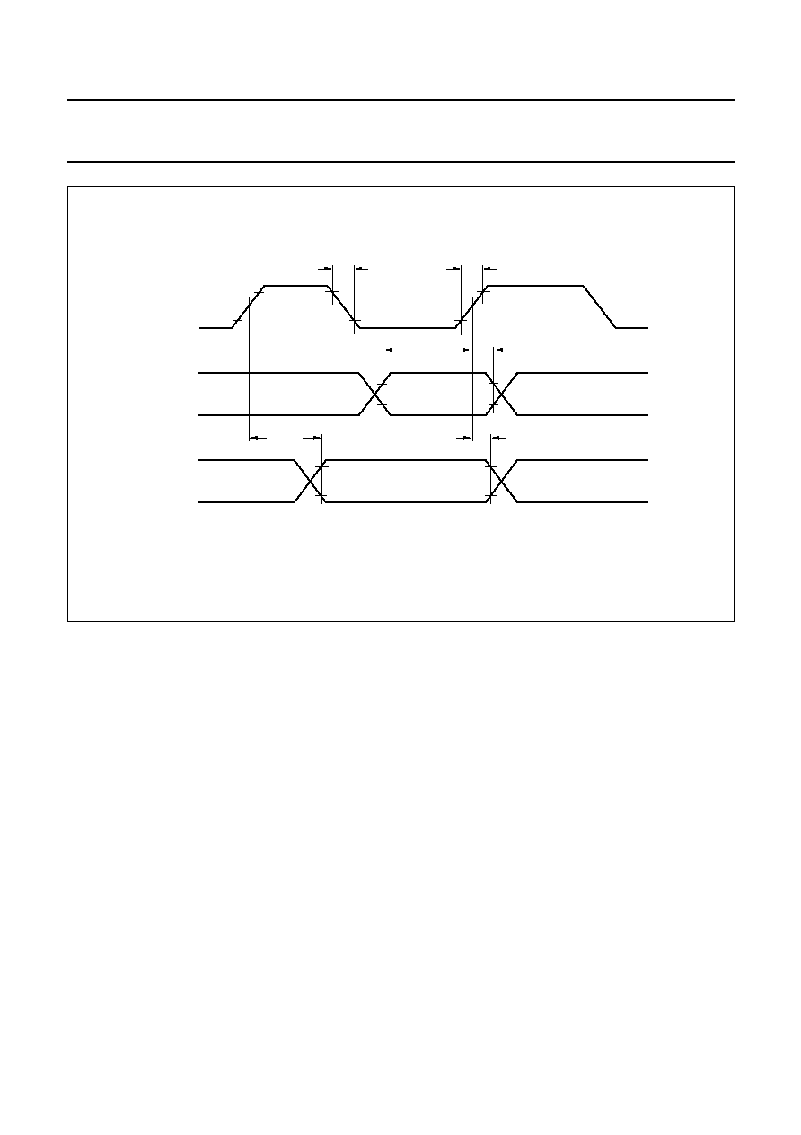
1999 Sep 27
36
Philips Semiconductors
Preliminary specification
Digital PC-camera signal processor
SAA8113HL
handbook, full pagewidth
FCE324
tsu(i)(D)
th(i)(D)
tf
tr
90%
90%
td(o)(D)
50%
XIN
data input
data output
10%
10%
10%
90%
th(o)(D)
10%
90%
Fig.13 Data input/output timing.
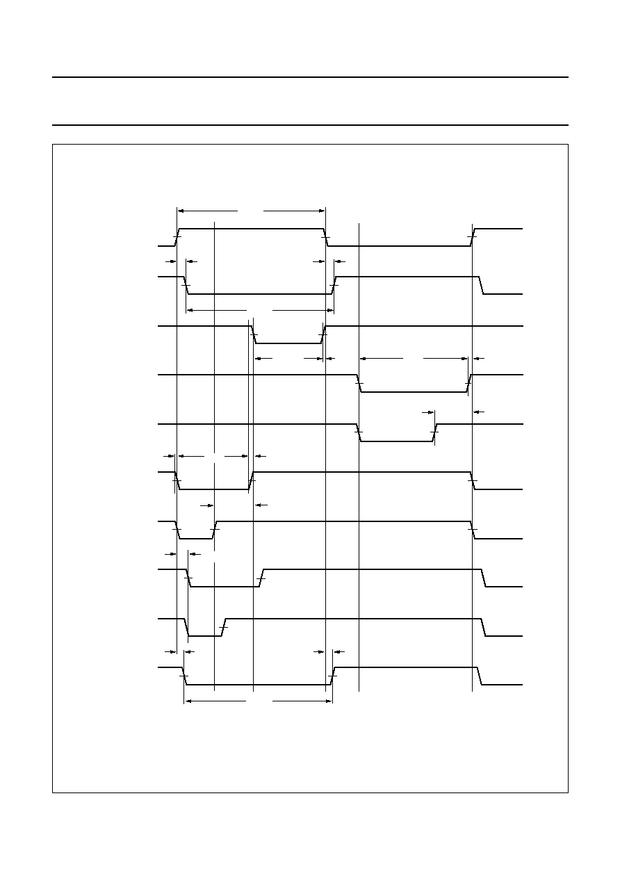
1999 Sep 27
37
Philips Semiconductors
Preliminary specification
Digital PC-camera signal processor
SAA8113HL
handbook, full pagewidth
FCE325
CLK1
FR_narrow_delayed
FR_wide_delayed
FR_narrow
FR_wide
FS_narrow
FS_wide
FCDS
FH2
FH1
twFH1
twFCDS
twFH2
td2
td5
td1
50%
50%
50%
twFS
td6_wide
td6_narrow
50%
50%
50%
50%
50%
50%
50%
50%
50%
twFR
twCLK1
td4_wide
td3
td4_narrow
td7
td3_delayed
td8
Fig.14 PPG high speed pulse timing diagram.
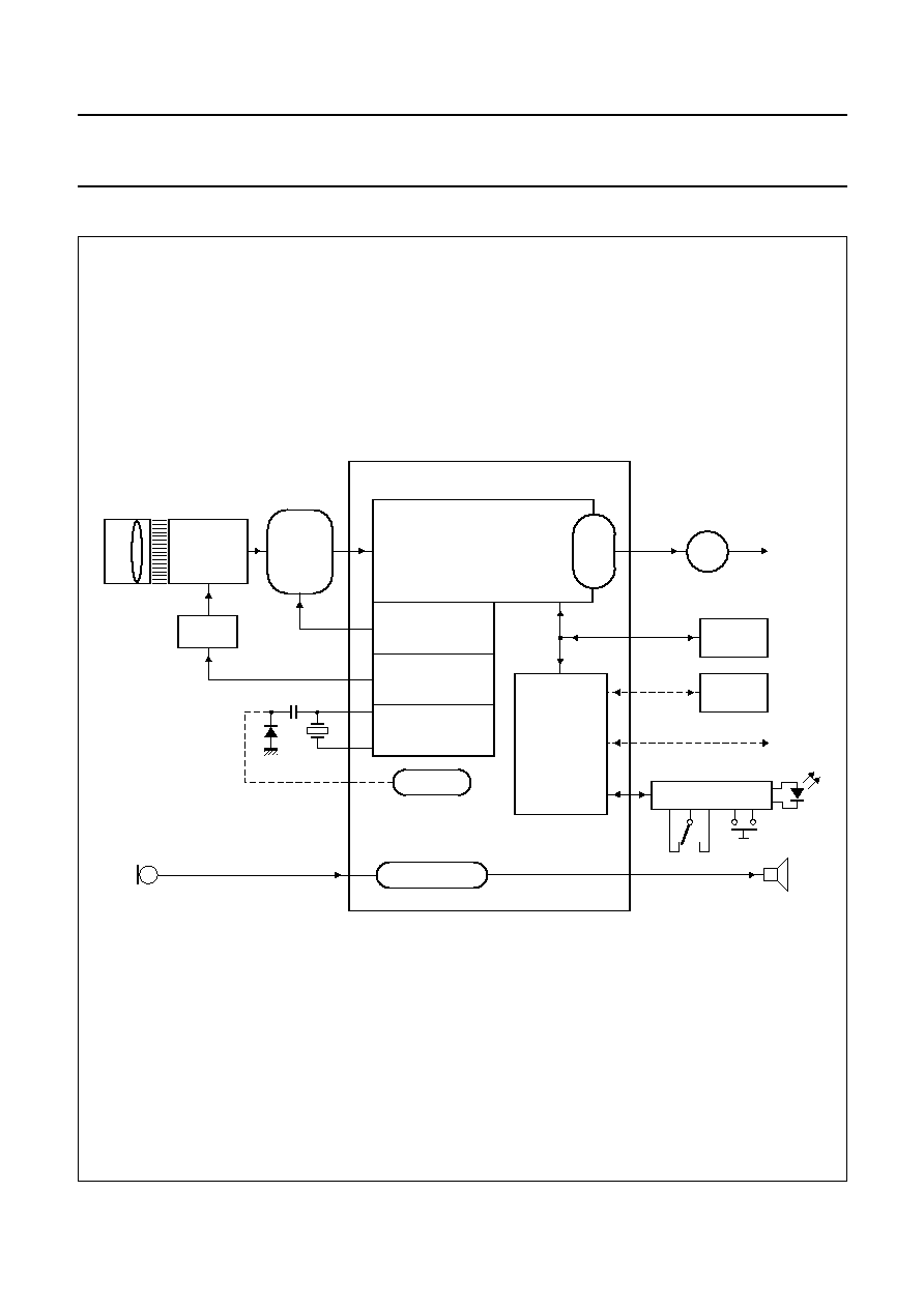
1999 Sep 27
38
Philips Semiconductors
Preliminary specification
Digital PC-camera signal processor
SAA8113HL
13 APPLICATION INFORMATION
handbook, full pagewidth
FCE326
analog
(CVBS)
program
PROM
settings
EEPROM
serial
interface
I
2
C-bus
interface
parallel
interface
HUMAN INTERFACE
CDAC
MICRO-
CONTROLLER
80C51
VDAC
SAA8113HL
DIGITAL
SIGNAL
PROCESSING
PREPROCESSING,
TIMING AND
CONTROL
SENSOR,
TIMING AND
CONTROL
DRIVERS
optics
analog
preprocessing
CCD sensor
PAL/NTSC
(medium
resolution)
CDS,
AGC
AND
ADC
MODE CONTROL
AND
CLOCK GENERATOR
LPF
AUDIO AMPLIFIER
Fig.15 Application block diagram.
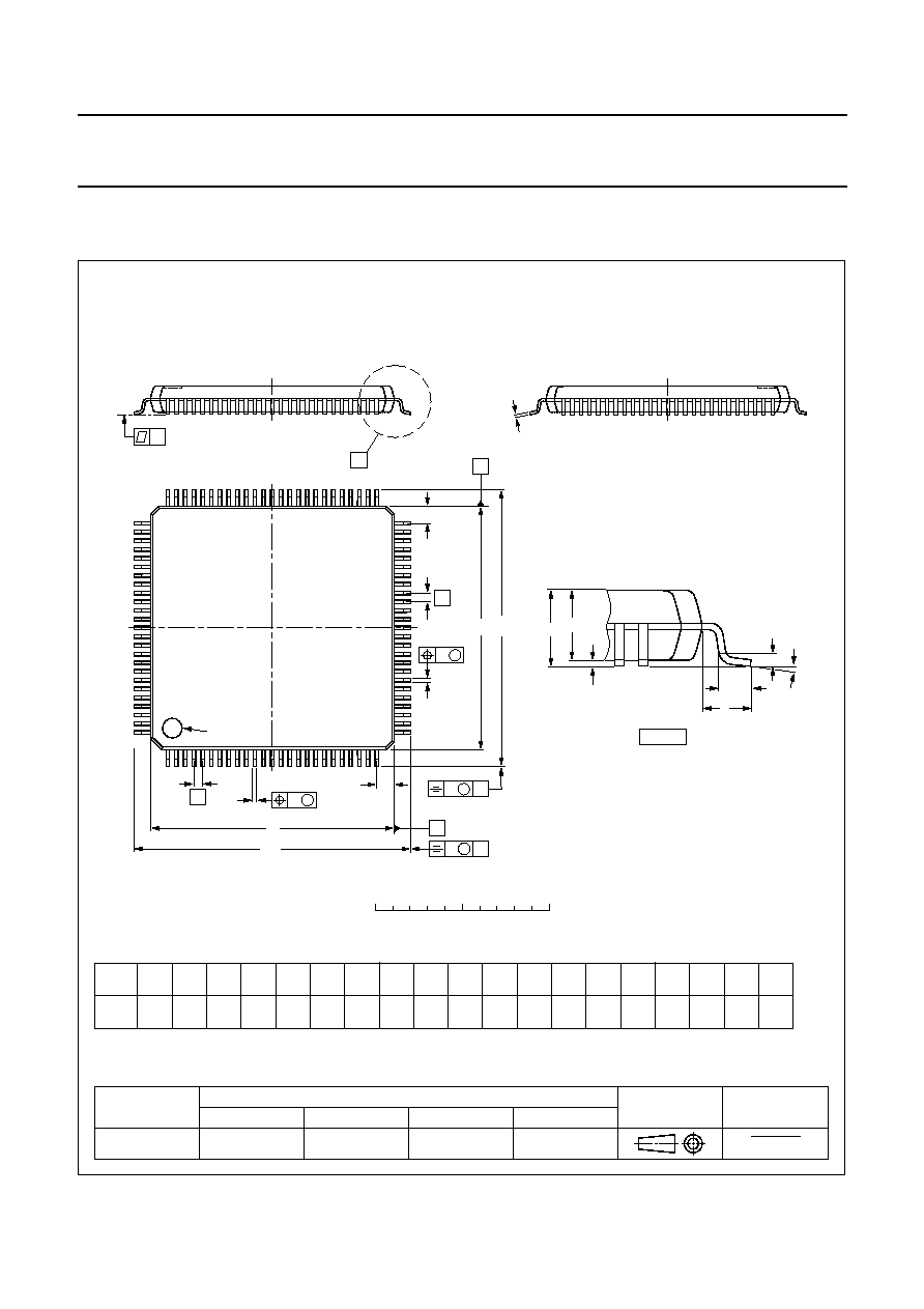
1999 Sep 27
39
Philips Semiconductors
Preliminary specification
Digital PC-camera signal processor
SAA8113HL
14 PACKAGE OUTLINE
UNIT
A
max.
A
1
A
2
A
3
b
p
c
E
(1)
e
H
E
L
L
p
Z
y
w
v
REFERENCES
OUTLINE
VERSION
EUROPEAN
PROJECTION
ISSUE DATE
IEC
JEDEC
EIAJ
mm
1.6
0.20
0.05
1.5
1.3
0.25
0.28
0.16
0.18
0.12
14.1
13.9
0.5
16.25
15.75
1.15
0.85
7
0
o
o
0.12
0.1
0.2
1.0
DIMENSIONS (mm are the original dimensions)
Note
1. Plastic or metal protrusions of 0.25 mm maximum per side are not included.
0.75
0.45
SOT407-1
95-12-19
97-08-04
D
(1)
(1)
(1)
14.1
13.9
H
D
16.25
15.75
E
Z
1.15
0.85
D
b
p
e
E
A
1
A
L
p
detail X
L
(A )
3
B
25
c
D
H
b
p
E
H
A
2
v
M
B
D
ZD
A
Z E
e
v
M
A
X
1
100
76
75
51
50
26
y
pin 1 index
w
M
w
M
0
5
10 mm
scale
LQFP100: plastic low profile quad flat package; 100 leads; body 14 x 14 x 1.4 mm
SOT407-1

1999 Sep 27
40
Philips Semiconductors
Preliminary specification
Digital PC-camera signal processor
SAA8113HL
15 SOLDERING
15.1
Introduction to soldering surface mount
packages
This text gives a very brief insight to a complex technology.
A more in-depth account of soldering ICs can be found in
our
"Data Handbook IC26; Integrated Circuit Packages"
(document order number 9398 652 90011).
There is no soldering method that is ideal for all surface
mount IC packages. Wave soldering is not always suitable
for surface mount ICs, or for printed-circuit boards with
high population densities. In these situations reflow
soldering is often used.
15.2
Reflow soldering
Reflow soldering requires solder paste (a suspension of
fine solder particles, flux and binding agent) to be applied
to the printed-circuit board by screen printing, stencilling or
pressure-syringe dispensing before package placement.
Several methods exist for reflowing; for example,
infrared/convection heating in a conveyor type oven.
Throughput times (preheating, soldering and cooling) vary
between 100 and 200 seconds depending on heating
method.
Typical reflow peak temperatures range from
215 to 250
∞
C. The top-surface temperature of the
packages should preferable be kept below 230
∞
C.
15.3
Wave soldering
Conventional single wave soldering is not recommended
for surface mount devices (SMDs) or printed-circuit boards
with a high component density, as solder bridging and
non-wetting can present major problems.
To overcome these problems the double-wave soldering
method was specifically developed.
If wave soldering is used the following conditions must be
observed for optimal results:
∑
Use a double-wave soldering method comprising a
turbulent wave with high upward pressure followed by a
smooth laminar wave.
∑
For packages with leads on two sides and a pitch (e):
≠ larger than or equal to 1.27 mm, the footprint
longitudinal axis is preferred to be parallel to the
transport direction of the printed-circuit board;
≠ smaller than 1.27 mm, the footprint longitudinal axis
must be parallel to the transport direction of the
printed-circuit board.
The footprint must incorporate solder thieves at the
downstream end.
∑
For packages with leads on four sides, the footprint must
be placed at a 45
∞
angle to the transport direction of the
printed-circuit board. The footprint must incorporate
solder thieves downstream and at the side corners.
During placement and before soldering, the package must
be fixed with a droplet of adhesive. The adhesive can be
applied by screen printing, pin transfer or syringe
dispensing. The package can be soldered after the
adhesive is cured.
Typical dwell time is 4 seconds at 250
∞
C.
A mildly-activated flux will eliminate the need for removal
of corrosive residues in most applications.
15.4
Manual soldering
Fix the component by first soldering two
diagonally-opposite end leads. Use a low voltage (24 V or
less) soldering iron applied to the flat part of the lead.
Contact time must be limited to 10 seconds at up to
300
∞
C.
When using a dedicated tool, all other leads can be
soldered in one operation within 2 to 5 seconds between
270 and 320
∞
C.

1999 Sep 27
41
Philips Semiconductors
Preliminary specification
Digital PC-camera signal processor
SAA8113HL
15.5
Suitability of surface mount IC packages for wave and reflow soldering methods
Notes
1. All surface mount (SMD) packages are moisture sensitive. Depending upon the moisture content, the maximum
temperature (with respect to time) and body size of the package, there is a risk that internal or external package
cracks may occur due to vaporization of the moisture in them (the so called popcorn effect). For details, refer to the
Drypack information in the
"Data Handbook IC26; Integrated Circuit Packages; Section: Packing Methods".
2. These packages are not suitable for wave soldering as a solder joint between the printed-circuit board and heatsink
(at bottom version) can not be achieved, and as solder may stick to the heatsink (on top version).
3. If wave soldering is considered, then the package must be placed at a 45
∞
angle to the solder wave direction.
The package footprint must incorporate solder thieves downstream and at the side corners.
4. Wave soldering is only suitable for LQFP, TQFP and QFP packages with a pitch (e) equal to or larger than 0.8 mm;
it is definitely not suitable for packages with a pitch (e) equal to or smaller than 0.65 mm.
5. Wave soldering is only suitable for SSOP and TSSOP packages with a pitch (e) equal to or larger than 0.65 mm; it is
definitely not suitable for packages with a pitch (e) equal to or smaller than 0.5 mm.
PACKAGE
SOLDERING METHOD
WAVE
REFLOW
(1)
BGA, SQFP
not suitable
suitable
HLQFP, HSQFP, HSOP, HTSSOP, SMS
not suitable
(2)
suitable
PLCC
(3)
, SO, SOJ
suitable
suitable
LQFP, QFP, TQFP
not recommended
(3)(4)
suitable
SSOP, TSSOP, VSO
not recommended
(5)
suitable

1999 Sep 27
42
Philips Semiconductors
Preliminary specification
Digital PC-camera signal processor
SAA8113HL
16 DEFINITIONS
17 LIFE SUPPORT APPLICATIONS
These products are not designed for use in life support appliances, devices, or systems where malfunction of these
products can reasonably be expected to result in personal injury. Philips customers using or selling these products for
use in such applications do so at their own risk and agree to fully indemnify Philips for any damages resulting from such
improper use or sale.
18 PURCHASE OF PHILIPS I
2
C COMPONENTS
Data sheet status
Objective specification
This data sheet contains target or goal specifications for product development.
Preliminary specification
This data sheet contains preliminary data; supplementary data may be published later.
Product specification
This data sheet contains final product specifications.
Limiting values
Limiting values given are in accordance with the Absolute Maximum Rating System (IEC 134). Stress above one or
more of the limiting values may cause permanent damage to the device. These are stress ratings only and operation
of the device at these or at any other conditions above those given in the Characteristics sections of the specification
is not implied. Exposure to limiting values for extended periods may affect device reliability.
Application information
Where application information is given, it is advisory and does not form part of the specification.
Purchase of Philips I
2
C components conveys a license under the Philips' I
2
C patent to use the
components in the I
2
C system provided the system conforms to the I
2
C specification defined by
Philips. This specification can be ordered using the code 9398 393 40011.

1999 Sep 27
43
Philips Semiconductors
Preliminary specification
Digital PC-camera signal processor
SAA8113HL
NOTES

© Philips Electronics N.V.
SCA
All rights are reserved. Reproduction in whole or in part is prohibited without the prior written consent of the copyright owner.
The information presented in this document does not form part of any quotation or contract, is believed to be accurate and reliable and may be changed
without notice. No liability will be accepted by the publisher for any consequence of its use. Publication thereof does not convey nor imply any license
under patent- or other industrial or intellectual property rights.
Internet: http://www.semiconductors.philips.com
1999
68
Philips Semiconductors ≠ a worldwide company
For all other countries apply to: Philips Semiconductors,
International Marketing & Sales Communications, Building BE-p, P.O. Box 218,
5600 MD EINDHOVEN, The Netherlands, Fax. +31 40 27 24825
Argentina: see South America
Australia: 3 Figtree Drive, HOMEBUSH, NSW 2140,
Tel. +61 2 9704 8141, Fax. +61 2 9704 8139
Austria: Computerstr. 6, A-1101 WIEN, P.O. Box 213,
Tel. +43 1 60 101 1248, Fax. +43 1 60 101 1210
Belarus: Hotel Minsk Business Center, Bld. 3, r. 1211, Volodarski Str. 6,
220050 MINSK, Tel. +375 172 20 0733, Fax. +375 172 20 0773
Belgium: see The Netherlands
Brazil: see South America
Bulgaria: Philips Bulgaria Ltd., Energoproject, 15th floor,
51 James Bourchier Blvd., 1407 SOFIA,
Tel. +359 2 68 9211, Fax. +359 2 68 9102
Canada: PHILIPS SEMICONDUCTORS/COMPONENTS,
Tel. +1 800 234 7381, Fax. +1 800 943 0087
China/Hong Kong: 501 Hong Kong Industrial Technology Centre,
72 Tat Chee Avenue, Kowloon Tong, HONG KONG,
Tel. +852 2319 7888, Fax. +852 2319 7700
Colombia: see South America
Czech Republic: see Austria
Denmark: Sydhavnsgade 23, 1780 COPENHAGEN V,
Tel. +45 33 29 3333, Fax. +45 33 29 3905
Finland: Sinikalliontie 3, FIN-02630 ESPOO,
Tel. +358 9 615 800, Fax. +358 9 6158 0920
France: 51 Rue Carnot, BP317, 92156 SURESNES Cedex,
Tel. +33 1 4099 6161, Fax. +33 1 4099 6427
Germany: Hammerbrookstraþe 69, D-20097 HAMBURG,
Tel. +49 40 2353 60, Fax. +49 40 2353 6300
Hungary: see Austria
India: Philips INDIA Ltd, Band Box Building, 2nd floor,
254-D, Dr. Annie Besant Road, Worli, MUMBAI 400 025,
Tel. +91 22 493 8541, Fax. +91 22 493 0966
Indonesia: PT Philips Development Corporation, Semiconductors Division,
Gedung Philips, Jl. Buncit Raya Kav.99-100, JAKARTA 12510,
Tel. +62 21 794 0040 ext. 2501, Fax. +62 21 794 0080
Ireland: Newstead, Clonskeagh, DUBLIN 14,
Tel. +353 1 7640 000, Fax. +353 1 7640 200
Israel: RAPAC Electronics, 7 Kehilat Saloniki St, PO Box 18053,
TEL AVIV 61180, Tel. +972 3 645 0444, Fax. +972 3 649 1007
Italy: PHILIPS SEMICONDUCTORS, Via Casati, 23 - 20052 MONZA (MI),
Tel. +39 039 203 6838, Fax +39 039 203 6800
Japan: Philips Bldg 13-37, Kohnan 2-chome, Minato-ku,
TOKYO 108-8507, Tel. +81 3 3740 5130, Fax. +81 3 3740 5057
Korea: Philips House, 260-199 Itaewon-dong, Yongsan-ku, SEOUL,
Tel. +82 2 709 1412, Fax. +82 2 709 1415
Malaysia: No. 76 Jalan Universiti, 46200 PETALING JAYA, SELANGOR,
Tel. +60 3 750 5214, Fax. +60 3 757 4880
Mexico: 5900 Gateway East, Suite 200, EL PASO, TEXAS 79905,
Tel. +9-5 800 234 7381, Fax +9-5 800 943 0087
Middle East: see Italy
Netherlands: Postbus 90050, 5600 PB EINDHOVEN, Bldg. VB,
Tel. +31 40 27 82785, Fax. +31 40 27 88399
New Zealand: 2 Wagener Place, C.P.O. Box 1041, AUCKLAND,
Tel. +64 9 849 4160, Fax. +64 9 849 7811
Norway: Box 1, Manglerud 0612, OSLO,
Tel. +47 22 74 8000, Fax. +47 22 74 8341
Pakistan: see Singapore
Philippines: Philips Semiconductors Philippines Inc.,
106 Valero St. Salcedo Village, P.O. Box 2108 MCC, MAKATI,
Metro MANILA, Tel. +63 2 816 6380, Fax. +63 2 817 3474
Poland: Al.Jerozolimskie 195 B, 02-222 WARSAW,
Tel. +48 22 5710 000, Fax. +48 22 5710 001
Portugal: see Spain
Romania: see Italy
Russia: Philips Russia, Ul. Usatcheva 35A, 119048 MOSCOW,
Tel. +7 095 755 6918, Fax. +7 095 755 6919
Singapore: Lorong 1, Toa Payoh, SINGAPORE 319762,
Tel. +65 350 2538, Fax. +65 251 6500
Slovakia: see Austria
Slovenia: see Italy
South Africa: S.A. PHILIPS Pty Ltd., 195-215 Main Road Martindale,
2092 JOHANNESBURG, P.O. Box 58088 Newville 2114,
Tel. +27 11 471 5401, Fax. +27 11 471 5398
South America: Al. Vicente Pinzon, 173, 6th floor,
04547-130 S√O PAULO, SP, Brazil,
Tel. +55 11 821 2333, Fax. +55 11 821 2382
Spain: Balmes 22, 08007 BARCELONA,
Tel. +34 93 301 6312, Fax. +34 93 301 4107
Sweden: Kottbygatan 7, Akalla, S-16485 STOCKHOLM,
Tel. +46 8 5985 2000, Fax. +46 8 5985 2745
Switzerland: Allmendstrasse 140, CH-8027 ZÐRICH,
Tel. +41 1 488 2741 Fax. +41 1 488 3263
Taiwan: Philips Semiconductors, 6F, No. 96, Chien Kuo N. Rd., Sec. 1,
TAIPEI, Taiwan Tel. +886 2 2134 2886, Fax. +886 2 2134 2874
Thailand: PHILIPS ELECTRONICS (THAILAND) Ltd.,
209/2 Sanpavuth-Bangna Road Prakanong, BANGKOK 10260,
Tel. +66 2 745 4090, Fax. +66 2 398 0793
Turkey: Yukari Dudullu, Org. San. Blg., 2.Cad. Nr. 28 81260 Umraniye,
ISTANBUL, Tel. +90 216 522 1500, Fax. +90 216 522 1813
Ukraine: PHILIPS UKRAINE, 4 Patrice Lumumba str., Building B, Floor 7,
252042 KIEV, Tel. +380 44 264 2776, Fax. +380 44 268 0461
United Kingdom: Philips Semiconductors Ltd., 276 Bath Road, Hayes,
MIDDLESEX UB3 5BX, Tel. +44 208 730 5000, Fax. +44 208 754 8421
United States: 811 East Arques Avenue, SUNNYVALE, CA 94088-3409,
Tel. +1 800 234 7381, Fax. +1 800 943 0087
Uruguay: see South America
Vietnam: see Singapore
Yugoslavia: PHILIPS, Trg N. Pasica 5/v, 11000 BEOGRAD,
Tel. +381 11 62 5344, Fax.+381 11 63 5777
Printed in The Netherlands
545006/25/01/pp
44
Date of release:
1999 Sep 27
Document order number:
9397 750 04816