 | –≠–ª–µ–∫—Ç—Ä–æ–Ω–Ω—ã–π –∫–æ–º–ø–æ–Ω–µ–Ω—Ç: SAA9740H | –°–∫–∞—á–∞—Ç—å:  PDF PDF  ZIP ZIP |
Document Outline
- FEATURES
- Auto Focus features
- Auto Exposure features
- Auto White Balance features
- GENERAL DESCRIPTION
- QUICK REFERENCE DATA
- ORDERING INFORMATION
- BLOCK DIAGRAM
- PINNING
- FUNCTIONAL DESCRIPTION
- AF system
- AE system
- AWB system
- Microprocessor interface
- LIMITING VALUES
- DC CHARACTERISTICS
- AC CHARACTERISTICS
- Microprocessor interface
- Data input/output timing (CLK1)
- MICROPROCESSOR COMMANDS
- Address 8BH
- Address 8CH and 8DH
- Address 8EH
- Address 8FH
- READ commands
- Register assignment
- APPLICATION INFORMATION
- PACKAGE OUTLINE
- SOLDERING
- DEFINITIONS
- LIFE SUPPORT APPLICATIONS

DATA SHEET
Product specification
Supersedes data of 1996 Jan 30
File under Integrated Circuits, IC02
1996 Oct 10
INTEGRATED CIRCUITS
SAA9740H
Advanced Auto Control Function
(A2CF)

1996 Oct 10
2
Philips Semiconductors
Product specification
Advanced Auto Control Function (A2CF)
SAA9740H
FEATURES
∑
One chip full digital Auto Focus (AF), Auto Exposure
(AE) and Auto White Balance (AWB)
∑
Possible to use NTSC and PAL CCD with horizontal
resolution of 510, 670, 720 or 768 pixels
∑
No manual adjustment
∑
One microprocessor system commonly used with
CAMera Digital Signal Processor (CAMDSP)
SAA9750H
∑
8-bit parallel microprocessor interface
∑
LQFP64 package (0.5 mm pitch)
∑
Single 3 V power supply.
Auto Focus features
∑
Video AF system
∑
Two windows system (a small centre and large window)
∑
The window size and place are microprocessor
controlled
∑
Including 5
th
order IIR digital high-pass filter
∑
Line peak accumulation in the large window
∑
High-pass filter's output accumulation in one field.
Auto Exposure features
∑
5 windows accumulation
∑
Calculation of white-clip by centre window
∑
Possible to control size and place of the centre windows
by the light condition with microprocessor.
Auto White Balance features
∑
Mono colour detection
∑
Accumulation of UV data in the corresponding UV
quadrant
∑
Green and Magenta elimination gate
∑
Luminance gate for detecting white
∑
UV limiter
∑
White-clip detection/counter.
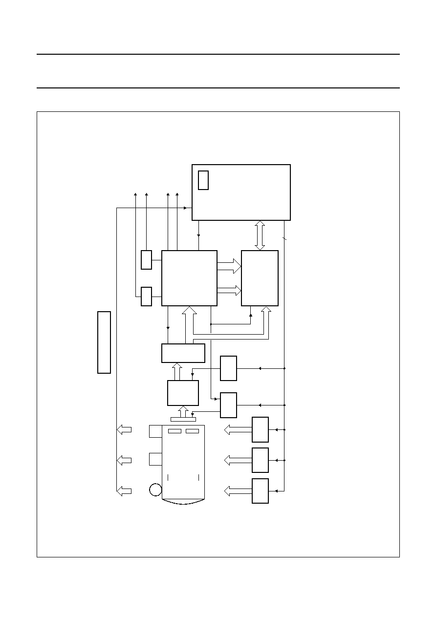
GENERAL DESCRIPTION
The Advanced Auto Control Function (A2CF) is to be used
for a colour CCD camera system. This IC can realize AWB,
AF and AE with a microprocessor. This device consists of
an input data selector, a parallel 8-bit microprocessor
interface, a data accumulator, a window generator, a
command decoder and AWB, AF, AE for each processing
block.
QUICK REFERENCE DATA
ORDERING INFORMATION
SYMBOL
PARAMETER
MIN.
TYP.
MAX.
UNIT
V
DD
digital supply voltage (pins 6, 18 and 47)
2.7
3.0
3.3
V
V
IL
LOW level digital input voltage
0
-
0.3V
DD
V
V
IH
HIGH level digital input voltage
0.7V
DD
-
V
DD
V
V
OL
LOW level digital output voltage
-
-
0.5
V
V
OH
HIGH level digital output voltage
V
DD
-
0.5
-
-
V
T
amb
operating ambient temperature
-
20
-
+70
∞
C
TYPE
NUMBER
PACKAGE
NAME
DESCRIPTION
VERSION
SAA9740H
LQFP64
plastic low profile quad flat package; 64 leads; body 10
◊
10
◊
1.4 mm
SOT314-2

1996
Oct
10
3
Philips Semiconductors
Product specification
Advanced Auto Control Function (A2CF)
SAA9740H
BLOCK DIAGRAM
Fig.1 Block diagram.
handbook, full pagewidth
CLOCK
GENERATOR
CLK1
1/2 CLK1
48
60
61 to 64, 1
AUTO
WHITE
BALANCE
8
AUTO
EXPOSURE
5
AUTO
FOCUS
16 to 9
57 to 50
8
PEAK
HOLD
18-BIT
ADDER
REGISTER
WHITE
CLIP
H/V
COUNTER
WINDOW
GENERATOR
MICROPROCESSOR
INTERFACE
34
33
35
8
6, 18, 47
LWDB
WDMNT
WDINT
37
36
32
ASTB
WRB
RDB
31
30
29
RSTB
28
IO7 to IO0
20 to 27
8
39, 38, 45 to 41
7
TSTOUT7
to
TSTOUT1
5
TST1
4
TSTIN3
3
TSTIN2
2
TSTIN1
17
WCLIP
58
SCAN_T
7, 19 46, 49, 59
VSS1 to VSS5
CLK2OUT
40
enable signals
CDS7
to
CDS0
Y7 to Y3
UV7 to UV0
CLK1
AMSAL
SAA9740H
VDD1 to VDD3
HD
VD
HSYNC
UV_SEL
MHA286
+
3 V

1996 Oct 10
4
Philips Semiconductors
Product specification
Advanced Auto Control Function (A2CF)
SAA9740H
PINNING
SYMBOL
PIN
TYPE
DESCRIPTION
Y3
1
input
Y input from SAA9750H (CAMDSP) (LSB)
TSTIN1
2
input
input pin for test
TSTIN2
3
input
input pin for test
TSTIN3
4
input
input pin for test
TST1
5
input
input pin for test
V
DD1
6
-
digital supply voltage
V
SS1
7
-
ground
UV_SEL
8
input
UV select input from SAA9750H (CAMDSP)
UV0
9
input
UV input from SAA9750H (CAMDSP) (LSB)
UV1
10
input
UV input from SAA9750H (CAMDSP)
UV2
11
input
UV input from SAA9750H (CAMDSP)
UV3
12
input
UV input from SAA9750H (CAMDSP)
UV4
13
input
UV input from SAA9750H (CAMDSP)
UV5
14
input
UV input from SAA9750H (CAMDSP)
UV6
15
input
UV input from SAA9750H (CAMDSP)
UV7
16
input
UV input from SAA9750H (CAMDSP) (MSB)
WCLIP
17
input
white-clip input from SAA9750H (CAMDSP)
V
DD2
18
-
digital supply voltage
V
SS2
19
-
ground
IO7
20
bidirectional
microprocessor interface (MSB)
IO6
21
bidirectional
microprocessor interface
IO5
22
bidirectional
microprocessor interface
IO4
23
bidirectional
microprocessor interface
IO3
24
bidirectional
microprocessor interface
IO2
25
bidirectional
microprocessor interface
IO1
26
bidirectional
microprocessor interface
IO0
27
bidirectional
microprocessor interface (LSB)
RSTB
28
input
system reset
RDB
29
input
read control from microprocessor
WRB
30
input
write control from microprocessor
ASTB
31
input
address set from microprocessor
WDINT
32
output
window interrupt
VD
33
input
V-drive signal input
HD
34
input
H-drive signal input
HSYNC
35
input
HSYNC input
WDMNT
36
output
window monitor for test (open-drain)
LWDB
37
output
large window for test (open-drain)
TSTOUT6
38
output
output pin for test
TSTOUT7
39
output
output pin for test
CLK2OUT
40
output
output pin of internal clock (open-drain)

1996 Oct 10
5
Philips Semiconductors
Product specification
Advanced Auto Control Function (A2CF)
SAA9740H
TSTOUT1
41
output
output pin for test
TSTOUT2
42
output
output pin for test
TSTOUT3
43
output
output pin for test
TSTOUT4
44
output
output pin for test
TSTOUT5
45
output
output pin for test
V
SS3
46
-
ground
V
DD3
47
-
digital supply voltage
CLK1
48
input
clock
V
SS4
49
-
ground
CDS0
50
input
CDS input from ADC (LSB)
CDS1
51
input
CDS input from ADC
CDS2
52
input
CDS input from ADC
CDS3
53
input
CDS input from ADC
CDS4
54
input
CDS input from ADC
CDS5
55
input
CDS input from ADC
CDS6
56
input
CDS input from ADC
CDS7
57
input
CDS input from ADC (MSB)
SCAN_T
58
input
test control for scan test
V
SS5
59
-
ground
AMSAL
60
input
for testing
Y7
61
input
Y input from SAA9750H (CAMDSP) (MSB)
Y6
62
input
Y input from SAA9750H (CAMDSP)
Y5
63
input
Y input from SAA9750H (CAMDSP)
Y4
64
input
Y input from SAA9750H (CAMDSP)
SYMBOL
PIN
TYPE
DESCRIPTION

1996 Oct 10
6
Philips Semiconductors
Product specification
Advanced Auto Control Function (A2CF)
SAA9740H
Fig.2 Pin configuration.
handbook, full pagewidth
SAA9740H
MHA285
1
2
3
4
5
6
7
8
9
10
11
12
13
14
15
16
48
47
46
45
44
43
42
41
40
39
38
37
36
35
34
33
17
18
19
20
21
22
23
24
25
26
27
28
29
30
31
32
64
63
62
61
60
59
58
57
56
55
54
53
52
51
50
49
CLK1
VDD3
VSS3
TSTOUT5
TSTOUT4
TSTOUT3
TSTOUT2
TSTOUT1
CLK2OUT
TSTOUT7
TSTOUT6
LWDB
WDMNT
HSYNC
HD
VD
WDINT
ASTB
WRB
RDB
RSTB
IO0
IO1
IO2
IO3
IO4
IO5
IO6
IO7
V
SS2
V
DD2
WCLIP
UV7
UV6
UV5
UV4
UV3
UV2
UV1
UV0
TST1
TSTIN3
TSTIN2
TSTIN1
Y3
VSS1
VDD1
UV_SEL
Y4
Y5
Y6
Y7
AMSAL
V
SS5
V
SS4
SCAN_T
CDS7
CDS6
CDS5
CDS4
CDS3
CDS2
CDS1
CDS0

1996 Oct 10
7
Philips Semiconductors
Product specification
Advanced Auto Control Function (A2CF)
SAA9740H
FUNCTIONAL DESCRIPTION
The Advanced Auto Control Function (A2CF) will be used
for colour CCD camera systems.
The input signals are CDS (AF data) from 8-bit ADC,
Y (for AE, 5-bit) and UV (for AWB, 8-bit) data as the output
of SAA9750H (CAMDSP) and they are fed into the A2CF.
After being processed in the A2CF, corresponding data
are led into the microprocessor.
Together with the zoom encoder and focus sensor output
the microprocessor does the following control with the data
of A2CF:
∑
Control focus motor
∑
Control iris, AGC (via DAC) and high speed shutter
∑
Send the control data to SAA9750H (CAMDSP) via
serial bus.
CLK1 is depending on the CCD type. To cope with the
different CCD clocks, some reference data have to be set
by the microprocessor.
AF system
Digital CDS signals CDS7 to CDS0 which come after
AGC, gamma processing and ADC are fed into A2CF.
This 8-bit data is shifted to the most suitable 6-bit data for
AF processing by microprocessor. For example, when the
MSB of them is `1' then the 6-bit data is shifted by the
microprocessor to CDS7 to CDS2
(not CDS6 to CDS1 or CDS5 to CDS0; see Table 4). After
AF shifting the signals go through an LPF and they are
down sampled. The down sampling is done by CLK2
(CLK1/2). In order to detect the high frequency component
for AF processing, one HPF is added. This output is the
focus value. Next peak hold block is for acquiring
maximum focus value of every line in one field.
Fig.3 AF window.
handbook, halfpage
centre
window
large window
MHA287
active video
This maximum focus value is accumulated in the AF
window (see Fig.3) by the 18-bit adder. The values in the
large window are stored in REG2 (see Table 7) and those
in the small window are stored in REG3 (see Table 7).
Which data is used is dependent on the software (see
Tables 6 and 7). Besides this accumulation, line peak
accumulation is also done. This data is the maximum value
in one field and is stored in REG0 (see Table 7).
AE system
5-bit Y signals Y7 to Y3 which come from SAA9750H are
fed into A2CF for AE processing. This signal is internally
extended to 6 bits by adding a `0' as new MSB. Next they
go through an LPF and they are down sampled in the
same way as AF processing. In order to prevent overflow
of the 18-bit adder block, 2 modes exist (see Table 4).
The first is H decimation is on or off. If H decimation is on,
then the data for AE processing is available in every other
line. The second mode is that the data for AE processing
is shifted to
1
/
2
or not. If the data is shifted to
1
/
2
, it is done
before down sampling and before the data going to the
18-bit adder becomes
1
/
2
. Both these modes are controlled
by the microprocessor. In AE mode there are 5 windows
as shown in Fig.4. These windows are controlled by the
microprocessor. The accumulation data in window 1 to
window 5 is respectively stored in REG1 to REG5 (see
Table 7). The white-clip count data in the centre window is
stored to the lower 5 bits of REG0 (see Table 7).
The upper 3 bits of REG0 is the overflow information in the
18-bit adder (see Table 7).
Fig.4 AE window.
handbook, halfpage
MHA288
active video
1
3
2
4
5

1996 Oct 10
8
Philips Semiconductors
Product specification
Advanced Auto Control Function (A2CF)
SAA9740H
AWB system
8-bit UV signals UV[7] to UV[0] which come from the
SAA9750H (CAMDSP) are fed into the A2CF for AWB
processing. First the 8-bit data is limited to 6-bits because
the necessary data for AWB processing is around the
white colour signal. Then these signals go through an LPF
and they are down sampled. They are separated to U and
V signals by using UV_SEL coming from SAA9750H
(CAMDSP). As shown in Table 1, in the large window
these signals are compared with the threshold that is set
by the microprocessor. If the conditions shown in Fig.8 are
valid, the data is available for AWB processing. If the
conditions aren't valid, the data is ignored. The available
data in the first to the 4th quadrant are stored in
respectively REG1 to REG4 (see Table 7). The AWB (
)
mode (see Table 4) is for detecting whether the picture is
mono colour or not. If the AWB (B
-
Y) or AWB (R
-
Y) or
AWB (
) (see Table 4) mode is active and white-clip or
AWB limited (as mentioned above), then the counts of
them are stored in the lower 5 bits of REG0 (see Table 7).
In the AWB Y mode the lower 4 bits of REG0 are contrast
peak data in one field and the 4th bit is the overflow
information of the AF (see Table 7).
Microprocessor interface
8-bit data bus and 3 control ports are prepared (WRB,
RDB and ASTB) for microprocessor interface in A2CF for
quick data access instead of serial bus. A2CF has 11 read
commands and 13 write commands.
LIMITING VALUES
In accordance with the Absolute Maximum Rating System (IEC 134).
Note
1. Equivalent to discharging a 100 pF capacitor through a 1.5 k
series resistor.
SYMBOL
PARAMETER
MIN.
MAX.
UNIT
V
DD
supply voltage
-
0.5
+5.0
V
P
tot
total power dissipation
-
83
mW
V
I
input voltage
-
0.5
V
DD
+ 0.5
V
V
O
output voltage
-
0.5
V
DD
+ 0.5
V
T
stg
storage temperature
-
65
+150
∞
C
T
amb
operating ambient temperature
-
20
+70
∞
C
V
es
electrostatic handling; note 1
-
2000
+2000
V
LTCH
latch-up protection
100
-
mA

1996 Oct 10
9
Philips Semiconductors
Product specification
Advanced Auto Control Function (A2CF)
SAA9740H
DC CHARACTERISTICS
T
amb
=
-
20 to +70
∞
C; V
DD
= 2.7 to 3.3 V; unless otherwise specified.
Note
1. 510H PAL; V
DD
= 3 V; all modes active.
SYMBOL
PARAMETER
CONDITIONS
MIN.
TYP.
MAX.
UNIT
I
DD
supply current
note 1
-
12
25
mA
Input pins (TSTIN1 to TSTIN3, TST1, UV_SEL, UV0 to UV7, Y3 to Y7, WCLIP, RSTB, RDB, WRB, ASTB, VD, HD,
HSYNC, CLK1, CDS0 to CDS7, SCAN_T and AMSAL)
V
IH
HIGH level input voltage
0.7V
DD
-
-
V
V
IL
LOW level input voltage
-
-
0.3V
DD
V
I
IH
HIGH level input current
V
IH
= V
DD
-
-
1
µ
A
I
IL
LOW level input current
V
IL
= V
SS
-
-
-
1
µ
A
Output pins (WDINT and TSTOUT1 to TSTOUT7; push pull output)
V
OH
HIGH level output voltage
I
OH
=
-
20
µ
A
V
DD
-
0.1
-
-
V
I
OH
=
-
4 mA
V
DD
-
0.5
-
-
V
V
OL
LOW level output voltage
I
OL
= +20
µ
A
-
-
0.1
V
I
OL
= +4 mA
-
-
0.5
V
Output pins (WDMNT, LWDB and CLK2OUT; open-drain)
V
OL
LOW level output voltage
I
OL
= +20
µ
A
-
-
0.1
V
I
OL
= +4 mA
-
-
0.5
V
I
OZ
3-state leakage current
V
O
= V
DD
-
-
5
µ
A
Bidirectional pins (IO0 to IO7)
V
OH
HIGH level output voltage
I
OH
=
-
20
µ
A
V
DD
-
0.1
-
-
V
I
OH
=
-
8 mA
V
DD
-
0.5
-
-
V
V
OL
LOW level output voltage
I
OL
= +20
µ
A
-
-
0.1
V
I
OL
= +8 mA
-
-
0.5
V
V
IH
HIGH level input voltage
0.7V
DD
-
-
V
V
IL
LOW level input voltage
-
-
0.3V
DD
V
I
IH
HIGH level input current
V
IH
= V
DD
-
-
1
µ
A
I
IL
LOW level input current
V
IL
= V
SS
-
-
-
1
µ
A
I
OZ
3-state leakage current
V
O
= V
DD
or V
SS
-
-
±
5
µ
A
1996 Oct 10
10
Philips Semiconductors
Product specification
Advanced Auto Control Function (A2CF)
SAA9740H
AC CHARACTERISTICS
Microprocessor interface
T
amb
=
-
20 to +70
∞
C; V
DD
= 2.7 to 3.3 V; V
IL
= 0 V; V
IH
= V
DD
; V
ref
= 0.5V
DD
; input t
r
and t
f
= 30 ns; see Fig.5; unless
otherwise specified.
SYMBOL
PARAMETER
CONDITIONS
MIN.
TYP.
MAX.
UNIT
t
suAD
address setup time
0.4
-
-
µ
s
t
hAD
address hold time
0.4
-
-
µ
s
t
AR
ASTB to RDB time
0.5
-
-
µ
s
t
W R
RDB width
1.0
-
-
µ
s
t
RRD
RDB to read data
R
L
= 1 k
-
-
0.8
µ
s
t
hRRD
RDB to read data hold time
R
L
= 1 k
-
-
0.1
µ
s
t
AW
ASTB to WRB time
0.5
-
-
µ
s
t
W W
WRB width
1.0
-
-
µ
s
t
suW
WRB setup time
0.4
-
-
µ
s
t
hW
WRB hold time
0.4
-
-
µ
s
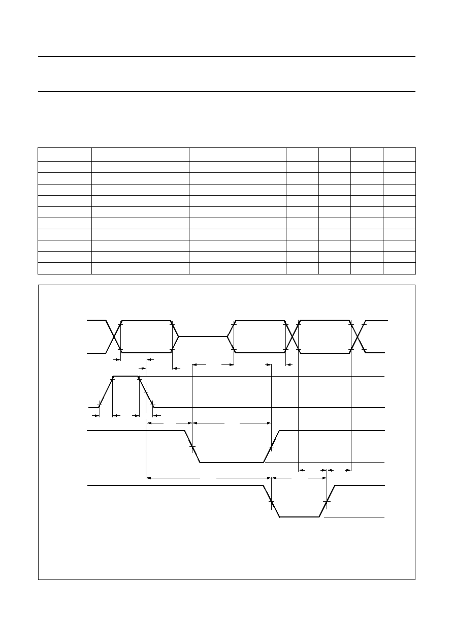
Fig.5 Microprocessor interface timing.
handbook, full pagewidth
MHA292
tsuW
thW
50%
50%
50%
50%
10%
10%
90%
90%
10%
90%
50%
tf
tr
tW W
tAR
tRRD
thRRD
thAD
tsuAD
tW R
tAW
read data
address
IO7 to IO0
ASTB
RDB
WRB
write data
VIH
VIL
VIH
VIL
VIH
VIL
VIH
VIL

1996 Oct 10
11
Philips Semiconductors
Product specification
Advanced Auto Control Function (A2CF)
SAA9740H
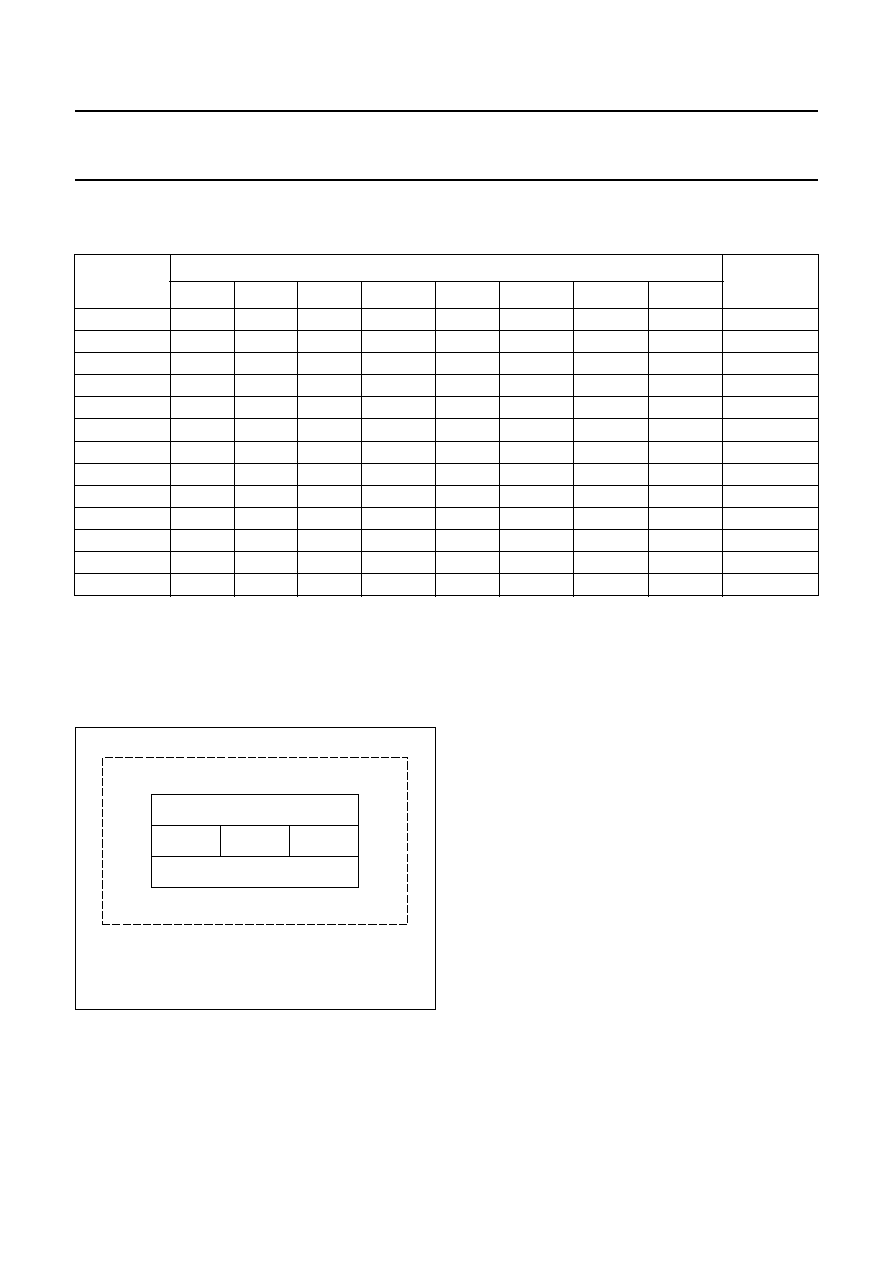
Data input/output timing (CLK1)
T
amb
=
-
20 to +70
∞
C; V
DD
= 2.7 to 3.3 V; V
IL
= 0 V; V
IH
= V
DD
; V
ref
= 0.5V
DD
; t
r
and t
f
= 6 ns; output load
capacitance = 20 pF; unless otherwise specified.
Notes
1. Data inputs: UV0 to UV7, Y3 to Y7, AD0 to AD7, UV_SEL, HSYNC, HD, VD and WCLIP.
2. Data outputs: WDINT, CLK2OUT, WDMNT and LWDB (open-drain outputs with 1 k
output load resistor).
3. T
amb
= 25
∞
C; V
DD
= 3.0 V.
SYMBOL
PARAMETER
CONDITIONS
MIN.
TYP.
MAX.
UNIT
t
suDI
data input setup time
note 1
5
-
-
ns
t
hDI
data input hold time
note 1
8
-
-
ns
t
dDO
data output delay time
notes 2 and 3
-
-
60
ns
t
hDO
data output hold time
notes 2 and 3
-
-
60
ns
t
W CLK1
width of CLK1
-
50
-
%
Fig.6 Data input/output timing (CLK1).
(1) 50% for open-drain outputs.
handbook, full pagewidth
MHA291
90%
CLK1
data inputs
data outputs
Vref
tf
10%
90%
10%
90%
10%
90%
10%
90%
10%
90%
VIH
VIL
VIH
VIL
VIH
VIL
10%
tr
tW CLK1
thDI
tdDO
tdDO
tsuDI
(1)
1996 Oct 10
12
Philips Semiconductors
Product specification
Advanced Auto Control Function (A2CF)
SAA9740H
MICROPROCESSOR COMMANDS
Table 1
Write commands; note 1
Notes
1. X = don't care.
2. For auto exposure processing different windows in the active video field are taken with different weighting factors.
The coordinates of the five windows are set according to Fig.7. The resolution is 1 bit
16 pixel in x-direction and
1 bit
8 lines in y-direction.
COMMAND
DATA
FUNCTION
IO7
IO6
IO5
IO4
IO3
IO2
IO1
IO0
81H
(2)
X
X
X1[5]
X1[4]
X1[3]
X1[2]
X1[1]
X1[0]
X1 address
82H
(2)
X
X
X2[5]
X2[4]
X2[3]
X2[2]
X2[1]
X2[0]
X2 address
83H
(2)
X
X
X3[5]
X3[4]
X3[3]
X3[2]
X3[1]
X3[0]
X3 address
84H
(2)
X
X
X4[5]
X4[4]
X4[3]
X4[2]
X4[1]
X4[0]
X4 address
85H
(2)
X
X
Y1[5]
Y1[4]
Y1[3]
Y1[2]
Y1[1]
Y1[0]
Y1 address
86H
(2)
X
X
Y2[5]
Y2[4]
Y2[3]
Y2[2]
Y2[1]
Y2[0]
Y2 address
87H
(2)
X
X
Y3[5]
Y3[4]
Y3[3]
Y3[2]
Y3[1]
Y3[0]
Y3 address
88H
(2)
X
X
Y4[5]
Y4[4]
Y4[3]
Y4[2]
Y4[1]
Y4[0]
Y4 address
8BH
X
TEST2
TEST1
TEST0
X
IIRC2
IIRC1
IIRC0
IIRC
8CH
THB[3]
THB[2]
THB[1]
THB[0]
THA[3]
THA[2]
THA[1]
THA[0]
TH1
8DH
X
X
X
X
THC[3]
THC[2]
THC[1]
THC[0]
TH2
8EH
SFTY
SFT1
SFT0
X
HON
MODE2
MODE1
MODE0
MODE
8FH
X
SIZE
MWD1
MWD0
X
PHS
PHD
PVD
SET
Fig.7
Window size control for AE processing
(see WRITE command 81H to 88H).
handbook, halfpage
active video
WIN1
WIN3
WIN2
X3/Y3
0/0
X1/Y1
X2/Y2
X4/Y4
MHA289
WIN4
WIN5

1996 Oct 10
13
Philips Semiconductors
Product specification
Advanced Auto Control Function (A2CF)
SAA9740H
Address 8BH
Table 2
IIRC (IO[2] to IO[0])
Table 3
IIRC 9IO[6] to 9IO[4]; note 1
Note
1. X = don't care.
Address 8CH and 8DH
Address 8CH and 8DH are used to define the active range that is taken for auto white balance processing.
The calculation of active area can be seen in Fig.8.
IIRC2
IIRC1
IIRC0
FUNCTION
0
0
0
1 MHz HPF select for auto focus processing
0
0
1
700 kHz HPF select for auto focus processing
0
1
0
220 kHz HPF select for auto focus processing
0
1
1
bypass HPF for auto focus processing
1
1
0
110 kHz select for auto focus processing
TEST2
TEST1
TEST0
FUNCTION
X
X
X
only for test purposes
handbook, full pagewidth
B
-
Y (U)
R
-
Y (V)
THB
THA
MHA290
-
THA
-
THB
Fig.8 Set threshold values for Auto White Balance (AWB) mode.
Conditions:
(1)
U + V
< THA.
(2)
V
< THB.
(3) Y > THC.
Threshold values can be set with 4-bit resolution.

1996 Oct 10
14
Philips Semiconductors
Product specification
Advanced Auto Control Function (A2CF)
SAA9740H
Address 8EH
By applying address 8EH and setting the MODE bits it is possible to read the values that are stored in the registers
corresponding to the selected mode. The selection which register will be read is then defined by READ address
70H to 7BH (see Tables 6 and 7).
Table 4
MODE and shift definition (see WRITE command 8EH); note 1
Note
1. X = don't care.
IO7
IO6
IO5
IO4
IO3
IO2
IO1
IO0
MODE
FUNCTION
SFTY SFT1
SFT0
-
HON
MODE MODE MODE
X
X
X
X
X
0
0
0
AE
set mode: read AE values
X
X
X
X
X
0
0
1
AF
set mode: read AF values
X
X
X
X
X
0
1
1
AWB (B
-
Y) set mode: read AWB (B
-
Y) values
X
X
X
X
X
1
0
0
AWB (R
-
Y) set mode: read AWB (R
-
Y) values
X
X
X
X
X
1
0
1
AWB
set mode: read AWB
values
X
X
X
X
X
1
1
0
AWB Y
set mode: read AWB Y values
X
X
X
X
0
0
0
0
H dec
decimation for 1H off
X
X
X
X
1
0
0
0
H dec
decimation for 1H on
X
0
0
X
X
0
0
1
AF shift
select CDS5 to CDS0 for AF
processing
X
0
1
X
X
0
0
1
AF shift
select CDS6 to CDS1 for AF
processing
X
1
X
X
X
0
0
1
AF shift
select CDS7 to CDS2 for AF
processing
0
X
X
X
X
0
0
0
AE shift
take AE[5] to AE[0] for internal AE
processing (see Chapter
"Functional description")
1
X
X
X
X
0
0
0
AE shift
take AE[5] to AE[1] for internal AE
processing (see Chapter
"Functional description")

1996 Oct 10
15
Philips Semiconductors
Product specification
Advanced Auto Control Function (A2CF)
SAA9740H
Address 8FH
To apply several types of CCDs it is possible to set polarity VD, HD and HSYNC by PVD, PHD and PHS.
The modes set by MWD and SIZE bit are only used for system evaluation. During normal application mode they can have
any value.
Table 5
Settings (see WRITE command 8FH); note 1
Note
1. X = don't care.
READ commands
The values of the internal registers can be read as follows:
1. Set mode AF, AE or AWB by WRITE command 8EH according to Table 4.
2. Select register by READ command 70H to 7BH according to Table 6.
Table 6
Read command
IO7
IO6
IO5
IO4
IO3
IO2
IO1
IO0
MODE
FUNCTION
-
SIZE
MWD1
MWD0
-
PHS
PHD
PVD
X
X
X
X
X
X
X
0
PVD
VD `H' active
X
X
X
X
X
X
X
1
PVD
VD `L' active
X
X
X
X
X
X
0
X
PHD
HD `H' active
X
X
X
X
X
X
1
X
PHD
HD `L' active
X
X
X
X
X
0
X
X
PHSYNC
HSYNC `H' active
X
X
X
X
X
1
X
X
PHSYNC
HSYNC `L' active
X
X
0
0
X
X
X
X
MWD AE
monitor AE window
X
X
0
1
X
X
X
X
MWD AF
monitor AF window
X
X
1
0
X
X
X
X
MWD AWB
monitor AWB window
X
X
1
1
X
X
X
X
MWD ALL
monitor all windows
X
0
X
X
X
X
X
X
MWD SMALL
monitor small window
X
1
X
X
X
X
X
X
MWD LARGE
monitor large window
COMMAND
DATA
FUNCTION
IO7
IO6
IO5
IO4
IO3
IO2
IO1
IO0
70H
O[15]
O[14]
O[13]
O[12]
O[11]
O[10]
O[9]
O[8]
REG1
71H
O[7]
O[6]
O[5]
O[4]
O[3]
O[2]
O[1]
O[0]
72H
O[15]
O[14]
O[13]
O[12]
O[11]
O[10]
O[9]
O[8]
REG2
73H
O[7]
O[6]
O[5]
O[4]
O[3]
O[2]
O[1]
O[0]
74H
O[15]
O[14]
O[13]
O[12]
O[11]
O[10]
O[9]
O[8]
REG3
75H
O[7]
O[6]
O[5]
O[4]
O[3]
O[2]
O[1]
O[0]
76H
O[15]
O[14]
O[13]
O[12]
O[11]
O[10]
O[9]
O[8]
REG4
77H
O[7]
O[6]
O[5]
O[4]
O[3]
O[2]
O[1]
O[0]
78H
O[15]
O[14]
O[13]
O[12]
O[11]
O[10]
O[9]
O[8]
REG5
79H
O[7]
O[6]
O[5]
O[4]
O[3]
O[2]
O[1]
O[0]
7BH
O[7]
O[6]
O[5]
O[4]
O[3]
O[2]
O[1]
O[0]
REG0

1996 Oct 10
16
Philips Semiconductors
Product specification
Advanced Auto Control Function (A2CF)
SAA9740H
Register assignment
For the different modes (AF, AE and AWB) the contents of the registers are assigned according to Table 7.
Table 7
Register assignment
MODE
REGISTER
DATA
FUNCTION
AF
REG0 (8-bit)
O[7] to O[5]
n.a.
O[4]
overflow information of AF block
O[3] to O[0]
contrast peak within one field
REG1 (18-bit)
O[15] to O[0] n.a.
REG2 (18-bit)
O[15] to O[0] accumulated data in the large window
REG3 (18-bit)
O[15] to O[0] accumulated data in the centre window
REG4 (18-bit)
O[15] to O[0] accumulated data of the large window minus the data of the centre
window
REG5 (18-bit)
O[15] to O[0] n.a.
AE
REG0 (8-bit)
O[7] to O[5]
18-bit adder overflow information
O[4] to O[0]
white-clip counter output
REG1 (18-bit)
O[15] to O[0] accumulated data in WIN1; REG1[18] to REG1[3]
REG2 (18-bit)
O[15] to O[0] accumulated data in WIN2; REG2[18] to REG2[3]
REG3 (18-bit)
O[15] to O[0] accumulated data in WIN3; REG3[18] to REG3[3]
REG4 (18-bit)
O[15] to O[0] accumulated data in WIN4; REG4[18] to REG4[3]
REG5 (18-bit)
O[15] to O[0] accumulated data in WIN5; REG5[18] to REG5[3]
AWB (B
-
Y) REG0 (8-bit)
O[7] to O[5]
n.a.
O[4] to O[0]
white-clip or AWB limiter count
REG1 (18-bit)
O[15] to O[0] accumulated B
-
Y data of 1st quadrant; REG1[18] to REG1[3]
REG2 (18-bit)
O[15] to O[0] accumulated B
-
Y data of 2nd quadrant; REG2[18] to REG2[3]
REG3 (18-bit)
O[15] to O[0] accumulated B
-
Y data of 3rd quadrant; REG3[18] to REG3[3]
REG4 (18-bit)
O[15] to O[0] accumulated B
-
Y data of 4th quadrant; REG4[18] to REG4[3]
REG5 (18-bit)
O[15] to O[0] n.a.
AWB (R
-
Y) REG0 (8-bit)
O[7] to O[5]
n.a.
O[4] to O[0]
white-clip or AWB limiter count
REG1 (18-bit)
O[15] to O[0] accumulated R
-
Y data of 1st quadrant; REG1[18] to REG1[3]
REG2 (18-bit)
O[15] to O[0] accumulated R
-
Y data of 2nd quadrant; REG2[18] to REG2[3]
REG3 (18-bit)
O[15] to O[0] accumulated R
-
Y data of 3rd quadrant; REG3[18] to REG3[3]
REG4 (18-bit)
O[15] to O[0] accumulated R
-
Y data of 4th quadrant; REG4[18] to REG4[3]
REG5 (18-bit)
O[15] to O[0] n.a.
AWB (
)
REG0 (8-bit)
O[7] to O[5]
n.a.
O[4] to O[0]
white-clip or AWB limiter count
REG1 (18-bit)
O[15] to O[0] accumulated
(R
-
Y) data of WIN1 to WIN5; REG1[18] to REG1[3]
REG2 (18-bit)
O[15] to O[0] accumulated
(B
-
Y) data of WIN1 to WIN5; REG2[18] to REG2[3]
REG3 (18-bit)
O[15] to O[0] accumulated
(R
-
Y) data of WIN3; REG3[18] to REG3[3]
REG4 (18-bit)
O[15] to O[0] accumulated
(B
-
Y) data of WIN3; REG4[18] to REG4[3]
REG5 (18-bit)
O[15] to O[0] n.a.

1996 Oct 10
17
Philips Semiconductors
Product specification
Advanced Auto Control Function (A2CF)
SAA9740H
AWB (Y)
REG0 (8-bit)
O[7] to O[5]
n.a.
O[4]
overflow information of auto focus block
O[3] to O[0]
contrast peak within one field
REG1 (18-bit)
O[15] to O[0] accumulated R
-
Y data of 1st quadrant; REG1[18] to REG1[3]
REG2 (18-bit)
O[15] to O[0] accumulated R
-
Y data of 2nd quadrant; REG2[18] to REG2[3]
REG3 (18-bit)
O[15] to O[0] accumulated R
-
Y data of 3rd quadrant; REG3[18] to REG3[3]
REG4 (18-bit)
O[15] to O[0] accumulated R
-
Y data of 4th quadrant; REG4[18] to REG4[3]
REG5 (18-bit)
O[15] to O[0] n.a.
MODE
REGISTER
DATA
FUNCTION
1996
Oct
10
18
Philips Semiconductors
Product specification
Advanced Auto Control Function (A2CF)
SAA9740H
APPLICA
TION INFORMA
TION
Fig.9 Camera block diagram (SAA9750H and SAA9740H).
handbook, full pagewidth
MHA293
CAMDSP
SIGNAL PROCESS
Y/C SEPARATION
SSG
ENCODER
SAA9750H
UV_SEL
HSYNC
WCLIP
UV7 to UV0
Y7 to Y3
A2CF
AF/AE/AWB
SAA9740H
HD, VD
8-bit
clamp
CDS7 to CDS0
ADC
CDS
AGC,
GAMMA
AGC
D/A
PPG
high speed
shuffle control
CCD
IRIS
DRIVER
focus
lens
iris
zoom
lens
MOTOR
DRIVER
MOTOR
DRIVER
focus
sensor
hall
sensor
zoom
encoder
LPF
BPF
serial
data bus
MICROPROCESSOR
ADC
3
IO7 to IO0
UV (8-bit)
Y (8-bit)
C
Y
CAMERA
1996 Oct 10
19
Philips Semiconductors
Product specification
Advanced Auto Control Function (A2CF)
SAA9740H
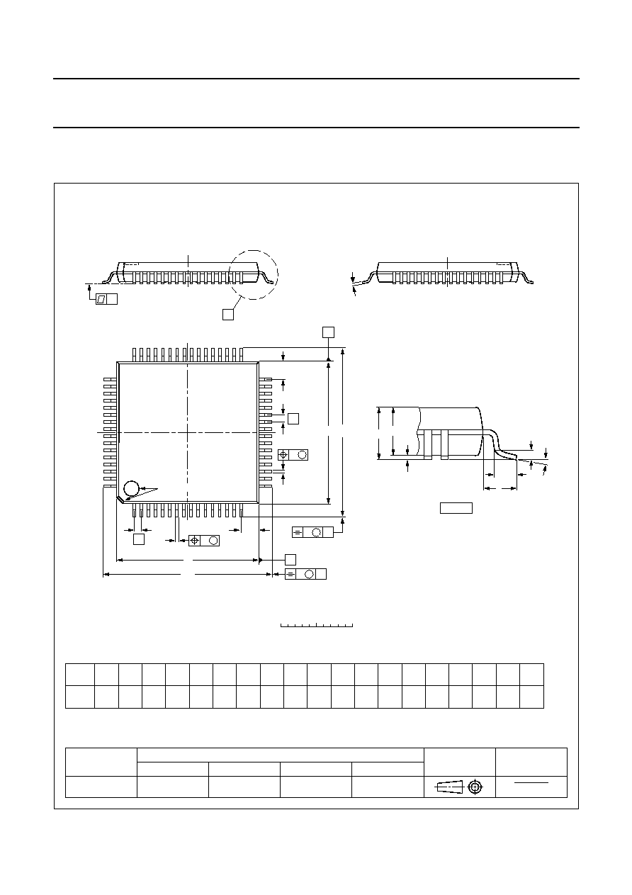
PACKAGE OUTLINE
UNIT
A
max.
A
1
A
2
A
3
b
p
c
E
(1)
e
H
E
L
L
p
Z
y
w
v
REFERENCES
OUTLINE
VERSION
EUROPEAN
PROJECTION
ISSUE DATE
IEC
JEDEC
EIAJ
mm
1.60
0.20
0.05
1.45
1.35
0.25
0.27
0.17
0.18
0.12
10.1
9.9
0.5
12.15
11.85
1.45
1.05
7
0
o
o
0.12
0.1
1.0
0.2
DIMENSIONS (mm are the original dimensions)
Note
1. Plastic or metal protrusions of 0.25 mm maximum per side are not included.
0.75
0.45
SOT314-2
95-12-19
97-08-01
D
(1)
(1)
(1)
10.1
9.9
H
D
12.15
11.85
E
Z
1.45
1.05
D
b
p
e
E
A
1
A
L
p
detail X
L
(A )
3
B
16
c
D
H
b
p
E
H
A
2
v
M
B
D
Z D
A
Z E
e
v
M
A
X
1
64
49
48
33
32
17
y
pin 1 index
w
M
w
M
0
2.5
5 mm
scale
LQFP64: plastic low profile quad flat package; 64 leads; body 10 x 10 x 1.4 mm
SOT314-2

1996 Oct 10
20
Philips Semiconductors
Product specification
Advanced Auto Control Function (A2CF)
SAA9740H
SOLDERING
Introduction
There is no soldering method that is ideal for all IC
packages. Wave soldering is often preferred when
through-hole and surface mounted components are mixed
on one printed-circuit board. However, wave soldering is
not always suitable for surface mounted ICs, or for
printed-circuits with high population densities. In these
situations reflow soldering is often used.
This text gives a very brief insight to a complex technology.
A more in-depth account of soldering ICs can be found in
our
"IC Package Databook" (order code 9398 652 90011).
Reflow soldering
Reflow soldering techniques are suitable for all LQFP
packages.
Reflow soldering requires solder paste (a suspension of
fine solder particles, flux and binding agent) to be applied
to the printed-circuit board by screen printing, stencilling or
pressure-syringe dispensing before package placement.
Several techniques exist for reflowing; for example,
thermal conduction by heated belt. Dwell times vary
between 50 and 300 seconds depending on heating
method. Typical reflow temperatures range from
215 to 250
∞
C.
Preheating is necessary to dry the paste and evaporate
the binding agent. Preheating duration: 45 minutes at
45
∞
C.
Wave soldering
Wave soldering is not recommended for LQFP packages.
This is because of the likelihood of solder bridging due to
closely-spaced leads and the possibility of incomplete
solder penetration in multi-lead devices.
If wave soldering cannot be avoided, the following
conditions must be observed:
∑
A double-wave (a turbulent wave with high upward
pressure followed by a smooth laminar wave)
soldering technique should be used.
∑
The footprint must be at an angle of 45
∞
to the board
direction and must incorporate solder thieves
downstream and at the side corners.
Even with these conditions, do not consider wave
soldering LQFP packages LQFP48 (SOT313-2),
LQFP64 (SOT314-2) or LQFP80 (SOT315-1).
During placement and before soldering, the package must
be fixed with a droplet of adhesive. The adhesive can be
applied by screen printing, pin transfer or syringe
dispensing. The package can be soldered after the
adhesive is cured.
Maximum permissible solder temperature is 260
∞
C, and
maximum duration of package immersion in solder is
10 seconds, if cooled to less than 150
∞
C within
6 seconds. Typical dwell time is 4 seconds at 250
∞
C.
A mildly-activated flux will eliminate the need for removal
of corrosive residues in most applications.
Repairing soldered joints
Fix the component by first soldering two diagonally-
opposite end leads. Use only a low voltage soldering iron
(less than 24 V) applied to the flat part of the lead. Contact
time must be limited to 10 seconds at up to 300
∞
C. When
using a dedicated tool, all other leads can be soldered in
one operation within 2 to 5 seconds between
270 and 320
∞
C.

1996 Oct 10
21
Philips Semiconductors
Product specification
Advanced Auto Control Function (A2CF)
SAA9740H
DEFINITIONS
LIFE SUPPORT APPLICATIONS
These products are not designed for use in life support appliances, devices, or systems where malfunction of these
products can reasonably be expected to result in personal injury. Philips customers using or selling these products for
use in such applications do so at their own risk and agree to fully indemnify Philips for any damages resulting from such
improper use or sale.
Data sheet status
Objective specification
This data sheet contains target or goal specifications for product development.
Preliminary specification
This data sheet contains preliminary data; supplementary data may be published later.
Product specification
This data sheet contains final product specifications.
Limiting values
Limiting values given are in accordance with the Absolute Maximum Rating System (IEC 134). Stress above one or
more of the limiting values may cause permanent damage to the device. These are stress ratings only and operation
of the device at these or at any other conditions above those given in the Characteristics sections of the specification
is not implied. Exposure to limiting values for extended periods may affect device reliability.
Application information
Where application information is given, it is advisory and does not form part of the specification.

1996 Oct 10
22
Philips Semiconductors
Product specification
Advanced Auto Control Function (A2CF)
SAA9740H
NOTES

1996 Oct 10
23
Philips Semiconductors
Product specification
Advanced Auto Control Function (A2CF)
SAA9740H
NOTES

Internet: http://www.semiconductors.philips.com
Philips Semiconductors ≠ a worldwide company
© Philips Electronics N.V. 1996
SCA52
All rights are reserved. Reproduction in whole or in part is prohibited without the prior written consent of the copyright owner.
The information presented in this document does not form part of any quotation or contract, is believed to be accurate and reliable and may be changed
without notice. No liability will be accepted by the publisher for any consequence of its use. Publication thereof does not convey nor imply any license
under patent- or other industrial or intellectual property rights.
Netherlands: Postbus 90050, 5600 PB EINDHOVEN, Bldg. VB,
Tel. +31 40 27 82785, Fax. +31 40 27 88399
New Zealand: 2 Wagener Place, C.P.O. Box 1041, AUCKLAND,
Tel. +64 9 849 4160, Fax. +64 9 849 7811
Norway: Box 1, Manglerud 0612, OSLO,
Tel. +47 22 74 8000, Fax. +47 22 74 8341
Philippines: Philips Semiconductors Philippines Inc.,
106 Valero St. Salcedo Village, P.O. Box 2108 MCC, MAKATI,
Metro MANILA, Tel. +63 2 816 6380, Fax. +63 2 817 3474
Poland: Ul. Lukiska 10, PL 04-123 WARSZAWA,
Tel. +48 22 612 2831, Fax. +48 22 612 2327
Portugal: see Spain
Romania: see Italy
Russia: Philips Russia, Ul. Usatcheva 35A, 119048 MOSCOW,
Tel. +7 095 247 9145, Fax. +7 095 247 9144
Singapore: Lorong 1, Toa Payoh, SINGAPORE 1231,
Tel. +65 350 2538, Fax. +65 251 6500
Slovakia: see Austria
Slovenia: see Italy
South Africa: S.A. PHILIPS Pty Ltd., 195-215 Main Road Martindale,
2092 JOHANNESBURG, P.O. Box 7430 Johannesburg 2000,
Tel. +27 11 470 5911, Fax. +27 11 470 5494
South America: Rua do Rocio 220, 5th floor, Suite 51,
04552-903 S„o Paulo, S√O PAULO - SP, Brazil,
Tel. +55 11 821 2333, Fax. +55 11 829 1849
Spain: Balmes 22, 08007 BARCELONA,
Tel. +34 3 301 6312, Fax. +34 3 301 4107
Sweden: Kottbygatan 7, Akalla, S-16485 STOCKHOLM,
Tel. +46 8 632 2000, Fax. +46 8 632 2745
Switzerland: Allmendstrasse 140, CH-8027 ZÐRICH,
Tel. +41 1 488 2686, Fax. +41 1 481 7730
Taiwan: PHILIPS TAIWAN Ltd., 23-30F, 66,
Chung Hsiao West Road, Sec. 1, P.O. Box 22978,
TAIPEI 100, Tel. +886 2 382 4443, Fax. +886 2 382 4444
Thailand: PHILIPS ELECTRONICS (THAILAND) Ltd.,
209/2 Sanpavuth-Bangna Road Prakanong, BANGKOK 10260,
Tel. +66 2 745 4090, Fax. +66 2 398 0793
Turkey: Talatpasa Cad. No. 5, 80640 GÐLTEPE/ISTANBUL,
Tel. +90 212 279 2770, Fax. +90 212 282 6707
Ukraine: PHILIPS UKRAINE, 4 Patrice Lumumba str., Building B, Floor 7,
252042 KIEV, Tel. +380 44 264 2776, Fax. +380 44 268 0461
United Kingdom: Philips Semiconductors Ltd., 276 Bath Road, Hayes,
MIDDLESEX UB3 5BX, Tel. +44 181 730 5000, Fax. +44 181 754 8421
United States: 811 East Arques Avenue, SUNNYVALE, CA 94088-3409,
Tel. +1 800 234 7381
Uruguay: see South America
Vietnam: see Singapore
Yugoslavia: PHILIPS, Trg N. Pasica 5/v, 11000 BEOGRAD,
Tel. +381 11 625 344, Fax.+381 11 635 777
For all other countries apply to: Philips Semiconductors, Marketing & Sales Communications,
Building BE-p, P.O. Box 218, 5600 MD EINDHOVEN, The Netherlands, Fax. +31 40 27 24825
Argentina: see South America
Australia: 34 Waterloo Road, NORTH RYDE, NSW 2113,
Tel. +61 2 9805 4455, Fax. +61 2 9805 4466
Austria: Computerstr. 6, A-1101 WIEN, P.O. Box 213,
Tel. +43 1 60 101, Fax. +43 1 60 101 1210
Belarus: Hotel Minsk Business Center, Bld. 3, r. 1211, Volodarski Str. 6,
220050 MINSK, Tel. +375 172 200 733, Fax. +375 172 200 773
Belgium: see The Netherlands
Brazil: see South America
Bulgaria: Philips Bulgaria Ltd., Energoproject, 15th floor,
51 James Bourchier Blvd., 1407 SOFIA,
Tel. +359 2 689 211, Fax. +359 2 689 102
Canada: PHILIPS SEMICONDUCTORS/COMPONENTS,
Tel. +1 800 234 7381
China/Hong Kong: 501 Hong Kong Industrial Technology Centre,
72 Tat Chee Avenue, Kowloon Tong, HONG KONG,
Tel. +852 2319 7888, Fax. +852 2319 7700
Colombia: see South America
Czech Republic: see Austria
Denmark: Prags Boulevard 80, PB 1919, DK-2300 COPENHAGEN S,
Tel. +45 32 88 2636, Fax. +45 31 57 1949
Finland: Sinikalliontie 3, FIN-02630 ESPOO,
Tel. +358 9 615800, Fax. +358 9 61580/xxx
France: 4 Rue du Port-aux-Vins, BP317, 92156 SURESNES Cedex,
Tel. +33 1 40 99 6161, Fax. +33 1 40 99 6427
Germany: Hammerbrookstraþe 69, D-20097 HAMBURG,
Tel. +49 40 23 53 60, Fax. +49 40 23 536 300
Greece: No. 15, 25th March Street, GR 17778 TAVROS/ATHENS,
Tel. +30 1 4894 339/239, Fax. +30 1 4814 240
Hungary: see Austria
India: Philips INDIA Ltd, Shivsagar Estate, A Block, Dr. Annie Besant Rd.
Worli, MUMBAI 400 018, Tel. +91 22 4938 541, Fax. +91 22 4938 722
Indonesia: see Singapore
Ireland: Newstead, Clonskeagh, DUBLIN 14,
Tel. +353 1 7640 000, Fax. +353 1 7640 200
Israel: RAPAC Electronics, 7 Kehilat Saloniki St, TEL AVIV 61180,
Tel. +972 3 645 0444, Fax. +972 3 649 1007
Italy: PHILIPS SEMICONDUCTORS, Piazza IV Novembre 3,
20124 MILANO, Tel. +39 2 6752 2531, Fax. +39 2 6752 2557
Japan: Philips Bldg 13-37, Kohnan 2-chome, Minato-ku, TOKYO 108,
Tel. +81 3 3740 5130, Fax. +81 3 3740 5077
Korea: Philips House, 260-199 Itaewon-dong, Yongsan-ku, SEOUL,
Tel. +82 2 709 1412, Fax. +82 2 709 1415
Malaysia: No. 76 Jalan Universiti, 46200 PETALING JAYA, SELANGOR,
Tel. +60 3 750 5214, Fax. +60 3 757 4880
Mexico: 5900 Gateway East, Suite 200, EL PASO, TEXAS 79905,
Tel. +9-5 800 234 7381
Middle East: see Italy
Printed in The Netherlands
537021/1200/02/pp24
Date of release: 1996 Oct 10
Document order number:
9397 750 01158