 | –≠–ª–µ–∫—Ç—Ä–æ–Ω–Ω—ã–π –∫–æ–º–ø–æ–Ω–µ–Ω—Ç: SAA9750H | –°–∫–∞—á–∞—Ç—å:  PDF PDF  ZIP ZIP |
Document Outline
- FEATURES
- GENERAL DESCRIPTION
- QUICK REFERENCE DATA
- ORDERING INFORMATION
- BLOCK DIAGRAM
- PINNING
- FUNCTIONAL DESCRIPTION
- LIMITING VALUES
- THERMAL CHARACTERISTICS
- DC CHARACTERISTICS
- DAC CHARACTERISTICS
- AC CHARACTERISTICS
- Microprocessor interface
- Data input/output timing (CLK1 and CLK2)
- SSG TIMING
- Clock count for NTSC and PAL mode
- Clock
- MICROPROCESSOR INTERFACE FORMAT
- MICROPROCESSOR SETTING
- CAMERA
- PACKAGE OUTLINE
- SOLDERING
- DEFINITIONS
- LIFE SUPPORT APPLICATIONS

DATA SHEET
Preliminary specification
File under Integrated Circuits, IC02
1996 Feb 16
INTEGRATED CIRCUITS
SAA9750H
Camera Digital Signal Processor
(CAMDSP)

1996 Feb 16
2
Philips Semiconductors
Preliminary specification
Camera Digital Signal Processor
(CAMDSP)
SAA9750H
FEATURES
∑
Y/C separator for mosaic filter colour CCD which can be
used with PAL or NTSC CCDs with horizontal resolution
of 510, 670, 720 or 768 pixels
∑
Line sequential colour processing (R
-
Y) and (B
-
Y)
∑
9 bit input signal (the internal processing is 10-bit)
∑
Digital feedback clamp control for Y/C separation
∑
Two 768
◊
9 line memories for Y/C separation
∑
Aperture correction using phase linear filters
∑
Coring of LOW level signals to reduce noise
∑
Colour encoder in accordance with the PAL or NTSC
system. Colour subcarrier is made by a discrete time
oscillator (DTO) operating on system clock
∑
Slew rate controlled outputs for reduction of digital noise
∑
RGB inputs for title mix
∑
High accuracy 8 bit DAC outputs for luminance and
chrominance signals
∑
Sync Signal Generator (SSG) to generate all necessary
timing signals
∑
Serial interface for microprocessor control of CAMDSP
settings
∑
Y and C signals accessible to incorporate digital
features
∑
Including digital feature functions (mosaic, sepia,
solarization, slice and negative/positive inversion).
GENERAL DESCRIPTION
The Camera Digital Signal Processor (CAMDSP) is
intended for use with a mosaic filter colour CCD. The IC
generates luminance and chrominance signals from the
CCD signal. The device consists of a luminance and colour
separator employing two 768
◊
9 line memories, a
PAL/NTSC encoder, a dual 8-bit video DAC, a Sync Signal
Generator (SSG) and a simple serial interface to control
many settings.
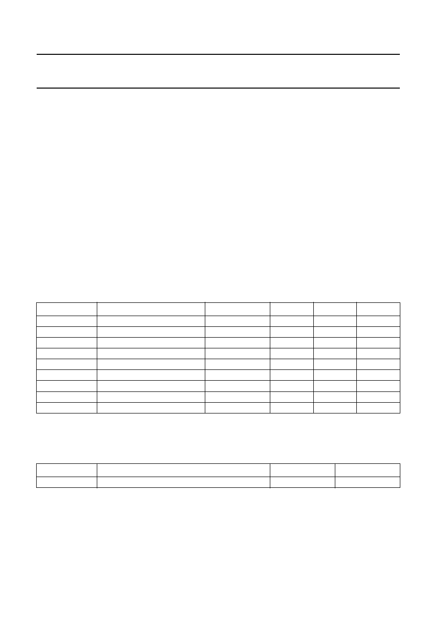
QUICK REFERENCE DATA
ORDERING INFORMATION
SYMBOL
PARAMETER
MIN.
TYP.
MAX.
UNIT
V
DDA1
Y-DAC analog supply voltage (pin 1)
2.7
3.0
3.3
V
V
DDA2
C-DAC analog supply voltage (pin 2)
2.7
3.0
3.3
V
V
DDD1
digital supply voltage (pin 41)
2.7
3.0
3.3
V
V
DDD2
digital supply voltage (pin 53)
2.7
3.0
3.3
V
V
DDD3
digital supply voltage (pin 65)
2.7
3.0
3.3
V
V
IH
HIGH level digital input voltage
0.7V
DDD
-
V
DDD
V
V
IL
LOW level digital input voltage
0
-
0.3V
DDD
V
V
OH
HIGH level digital output voltage
V
DDD
-
0.5
-
-
V
V
OL
LOW level digital output voltage
-
-
0.5
V
T
amb
operating ambient temperature
-
20
-
+70
∞
C
TYPE
NUMBER
PACKAGE
NAME
DESCRIPTION
VERSION
SAA9750H
LQFP80
plastic low profile quad flat package; 80 leads; body 12
◊
12
◊
1.4 mm
SOT315-1

1996
Feb
16
3
Philips Semiconductors
Preliminary specification
Camera Digital Signal Processor
(CAMDSP)
SAA9750H
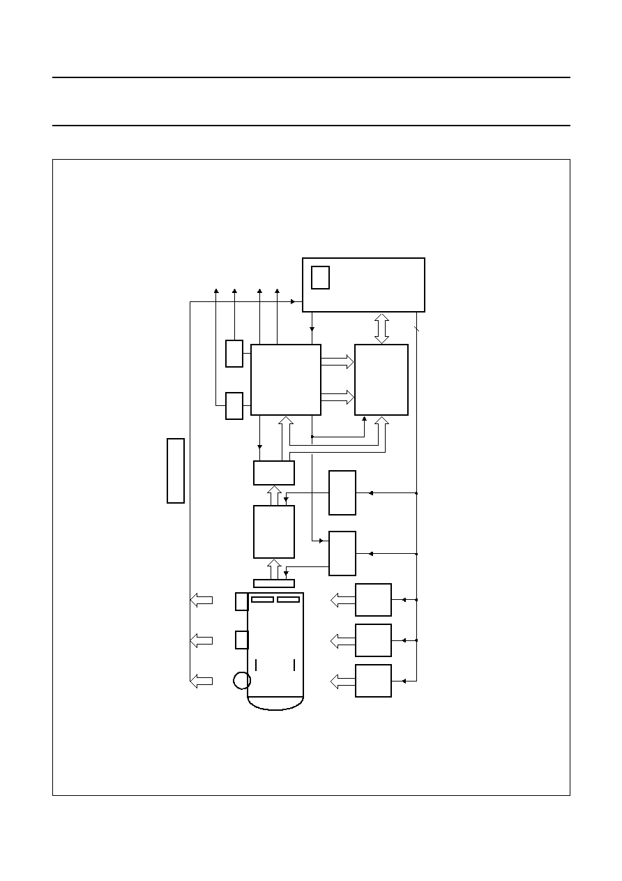
BLOCK DIAGRAM
handbook, full pagewidth
MICROPROCESSOR
INTERFACE
Y PROCESSING
C PROCESSING
FIFO
768
◊
9
FIFO
768
◊
9
CLAMP
X0H
Y settings
CLAMP
settings
C settings
X1H
X2H
TITLE
SWITCH
ENCODER
DELAY
YENC
sync
12 to 19
43 to 50
title mix
UVENC
title mix
SYNC SIGNAL
GENERATOR
30
62
CPOB
CLAMP
CS
CK
DI
VRST
HRST
CLK1
CLK2
CSYNC
HD
FLD
SYNCI
VSSA1
VSSA2
Y0 to Y7
TEST1 TEST2
VD
CP2
HSYNC
61
9
68 to 76
59
CLOCK
55
77
6
56
63
57
58
8
8
29
20
8 9 10 11 7
1
2
A
D
21 to 28
33 to 40
ENCODER
settings
SSG
settings
31
32
51
52
66
67
+
8
8
8
A
D
8
4
79
80
YENC7 to
YENC0
UVENC0 to
UVENC7
3
78
VrefY
VrefC
YOUT
COUT
VDDA2
VDDA1
VDDD1
VDDD3
VDDD2
UVSEL
LSW
TSW
WCLIP
UV0 to
UV7
CDS0 to
CDS8
B
G
R
MHA302
5
60
41
53
65
SAA9750H
VSSD2
64
VSSD3
54
VSSD1
42
Fig.1 Block diagram.

1996 Feb 16
4
Philips Semiconductors
Preliminary specification
Camera Digital Signal Processor
(CAMDSP)
SAA9750H
PINNING
SYMBOL
PIN
INPUT/OUTPUT
ANALOG/DIGITAL
DESCRIPTION
V
DDA1
1
supply
-
analog supply voltage 1 for Y-DAC
V
DDA2
2
supply
-
analog supply voltage 2 for C-DAC
C
OUT
3
output
analog
C-DAC output
V
SSA1
4
supply
-
analog ground 1 for C-DAC
V
refC
5
-
-
C-DAC decoupling voltage
TEST2
6
input
digital
test 2 pin
LSW
7
input
digital
line switch for SECAM
TSW
8
input
digital
title memory switch
R
9
input
digital
title memory colour (red)
G
10
input
digital
title memory colour (green)
B
11
input
digital
title memory colour (blue)
UV
ENC0
12
input
digital
B
-
Y and R
-
Y signal to encoder (LSB)
UV
ENC1
13
input
digital
B
-
Y and R
-
Y signal to encoder
UV
ENC2
14
input
digital
B
-
Y and R
-
Y signal to encoder
UV
ENC3
15
input
digital
B
-
Y and R
-
Y signal to encoder
UV
ENC4
16
input
digital
B
-
Y and R
-
Y signal to encoder
UV
ENC5
17
input
digital
B
-
Y and R
-
Y signal to encoder
UV
ENC6
18
input
digital
B
-
Y and R
-
Y signal to encoder
UV
ENC7
19
input
digital
B
-
Y and R
-
Y signal to encoder (MSB)
WCLIP
20
output
digital
white-clip
UV
7
21
output
digital
time multiplexed B
-
Y and R
-
Y (MSB)
UV
6
22
output
digital
time multiplexed B
-
Y and R
-
Y
UV
5
23
output
digital
time multiplexed B
-
Y and R
-
Y
UV
4
24
output
digital
time multiplexed B
-
Y and R
-
Y
UV
3
25
output
digital
time multiplexed B
-
Y and R
-
Y
UV
2
26
output
digital
time multiplexed B
-
Y and R
-
Y
UV
1
27
output
digital
time multiplexed B
-
Y and R
-
Y
UV
0
28
output
digital
time multiplexed B
-
Y and R
-
Y (LSB)
UV
SEL
29
output
digital
B
-
Y or R
-
Y active at UV output
CS
30
input
digital
microprocessor interface (chip select)
CK
31
input
digital
microprocessor interface (clock)
DI
32
input
digital
microprocessor interface (data input)
Y
0
33
output
digital
luminance signal (LSB)
Y
1
34
output
digital
luminance signal
Y
2
35
output
digital
luminance signal
Y
3
36
output
digital
luminance signal
Y
4
37
output
digital
luminance signal
Y
5
38
output
digital
luminance signal
Y
6
39
output
digital
luminance signal
Y
7
40
output
digital
luminance signal (MSB)

1996 Feb 16
5
Philips Semiconductors
Preliminary specification
Camera Digital Signal Processor
(CAMDSP)
SAA9750H
V
DDD1
41
supply
-
digital supply voltage 1
V
SSD1
42
supply
-
digital ground 1
Y
ENC7
43
input
digital
luminance signal to encoder (MSB)
Y
ENC6
44
input
digital
luminance signal to encoder
Y
ENC5
45
input
digital
luminance signal to encoder
Y
ENC4
46
input
digital
luminance signal to encoder
Y
ENC3
47
input
digital
luminance signal to encoder
Y
ENC2
48
input
digital
luminance signal to encoder
Y
ENC1
49
input
digital
luminance signal to encoder
Y
ENC0
50
input
digital
luminance signal to encoder (LSB)
VRST
51
input
digital
external VD (vertical drive)
HRST
52
input
digital
external HD (horizontal drive)
V
DDD3
53
supply
-
digital supply voltage 3
V
SSD3
54
supply
-
digital ground 3
VD
55
output
digital
VD timing for PPG IC
HD
56
output
digital
HD timing for PPG IC
FLD
57
output
digital
field pulse output
HSYNC
58
output
digital
horizontal timing for YC processing
CSYNC
59
output
digital
composite sync pulse
SYNCI
60
input
digital
sync input for bypass mode
CLAMP
61
output (3-state)
digital
clamp voltage control
CPOB
62
input
digital
optical black pulse
CP2
63
output
digital
clamping pulse
V
SSD2
64
supply
-
digital ground 2
V
DDD2
65
supply
-
digital supply voltage 2
CLK1
66
input
digital
clock 1
CLK2
67
input
digital
clock 2
CDS
0
68
input
digital
CDS signal (LSB)
CDS
1
69
input
digital
CDS signal
CDS
2
70
input
digital
CDS signal
CDS
3
71
input
digital
CDS signal
CDS
4
72
input
digital
CDS signal
CDS
5
73
input
digital
CDS signal
CDS
6
74
input
digital
CDS signal
CDS
7
75
input
digital
CDS signal
CDS
8
76
input
digital
CDS signal (MSB)
TEST1
77
input
digital
test 1 pin
V
refY
78
-
-
Y-DAC decoupling voltage
V
SSA2
79
supply
-
analog ground 2 for Y-DAC
Y
OUT
80
output
analog
Y-DAC output
SYMBOL
PIN
INPUT/OUTPUT
ANALOG/DIGITAL
DESCRIPTION

1996 Feb 16
6
Philips Semiconductors
Preliminary specification
Camera Digital Signal Processor
(CAMDSP)
SAA9750H
Fig.2 Pin configuration.
handbook, full pagewidth
SAA9750H
MHA301
1
2
3
4
5
6
7
8
9
10
11
12
13
14
15
16
17
18
19
20
VDDA1
VDDA2
COUT
VSSA1
VrefC
TEST2
LSW
TSW
R
G
B
UVENC0
UVENC1
UVENC2
UVENC3
UVENC4
UVENC5
UVENC6
UVENC7
WCLIP
SYNCI
CSYNC
HSYNC
FLD
HD
VD
VSSD3
VDDD3
HRST
VRST
YENC0
YENC1
YENC2
YENC3
YENC4
YENC5
YENC6
YENC7
VSSD1
VDDD1
60
59
58
57
56
55
54
53
52
51
50
49
48
47
46
45
44
43
42
41
21
22
23
24
25
26
27
28
29
30
31
32
33
34
35
36
37
38
39
40
UV
7
UV
6
UV
5
UV
4
UV
3
UV
2
UV
1
UV
0
UV
SEL
CS
CK
DI
Y
0
Y
1
Y
2
Y
3
Y
4
Y
5
Y
6
Y
7
Y
OUT
V
SSA2
V
refY
TEST1
CDS
8
CDS
7
CDS
6
CDS
5
CDS
4
CDS
3
CDS
2
CDS
1
CDS
0
CLK2
CLK1
V
DDD2
V
SSD2
CP2
CPOB
CLAMP
80
79
78
77
76
75
74
73
72
71
70
69
68
67
66
65
64
63
62
61
1996 Feb 16
7
Philips Semiconductors
Preliminary specification
Camera Digital Signal Processor
(CAMDSP)
SAA9750H
FUNCTIONAL DESCRIPTION
The Camera Digital Signal Processor (CAMDSP) is
intended for use with a mosaic filter colour CCD.
The input signal is an 8-bit or 9-bit digitized CCD signal.
After AGC and gamma correction, clamping of the input
signal is achieved by feedback clamp level control.
In the luminance processing, symmetrical horizontal and
vertical aperture correction are carried out. Coring is also
carried out to reduce noise at LOW signal levels. In the
chrominance processing, white balance control and matrix
control is adjustable. A false colour correction circuit
reduces aliasing of high frequency input signals.
A white-clip makes the colour white at highlights.
In the encoder part, the colour encoder subcarrier is made
by the discrete time oscillator thus eliminating the use of an
extra crystal. The subcarrier frequency for PAL or NTSC is
selectable. The encoding can be in PAL or NTSC format.
The encoded signal is output via separate 8-bit
digital-to-analog converters (DACs) for luminance and
chrominance. In the event of SECAM the output is a line
sequential
-
(R
-
Y)/(B
-
Y) signal. A line memory interface
allows for mixing of RGB signals in the main signal.
The encoder can be bypassed completely, in this event
only the title mix is carried out before digital-to-analog
conversion.
The SSG generates all necessary timing signals. Timing
signals for external devices NTSC, PAL and SECAM are
also made. The SSG can be locked to an external video
source.
CAMDSP can operate with 510H, 670H, 720H and 768H
colour mosaic CCDs both PAL and NTSC type. In the
510H CCD application the upsampling clock is used for the
encoder part, therefore two clock frequencies (f
s
and 2f
s
)
are required.
LIMITING VALUES
In accordance with the Absolute Maximum Rating System (IEC 134).
Note
1. Equivalent to discharging a 100 pF capacitor via a 1.5 k
series resistor.
THERMAL CHARACTERISTICS
SYMBOL
PARAMETER
CONDITIONS
MIN.
MAX.
UNIT
V
DDD
digital supply voltage
-
0.5
+5.0
V
V
DDA
analog supply voltage
-
0.5
+5.0
V
P
tot
total power dissipation
-
500
mW
V
I
digital input voltage
-
0.5
V
DDD
+ 0.5
V
V
O
digital output voltage
-
0.5
V
DDD
+ 0.5
V
T
stg
storage temperature
-
65
+150
∞
C
T
amb
operating ambient temperature
-
20
+70
∞
C
V
es
electrostatic handling
note 1
-
2000
+2000
V
I
latch
latch-up protection current
100
-
mA
SYMBOL
PARAMETER
VALUE
UNIT
R
th j-a
thermal resistance from junction to ambient in free air
57
K/W
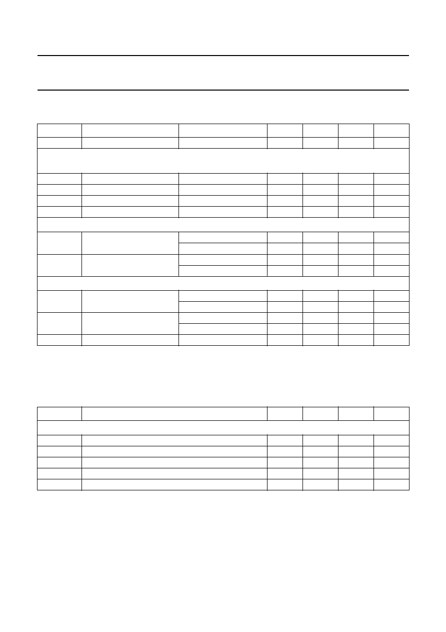
1996 Feb 16
8
Philips Semiconductors
Preliminary specification
Camera Digital Signal Processor
(CAMDSP)
SAA9750H
DC CHARACTERISTICS
V
DD
= 2.7 to 3.3 V; T
amb
=
-
20 to +70
∞
C; unless otherwise specified.
Note
1. 510H PAL; V
DD
= 3 V; DAC R
L
= 2 k
.
DAC CHARACTERISTICS
V
DD
= 3.0 V; T
amb
= +25
∞
C; R
L
= open-circuit; unless otherwise specified.
SYMBOL
PARAMETER
CONDITIONS
MIN.
TYP.
MAX.
UNIT
I
DD
supply current
note 1
-
60
150
mA
Inputs: LSW, TSW, R, G, B, UV
ENC0
to UV
ENC7
, CS, CK, DI, Y
ENC0
to Y
ENC7
, VRST, HRST, SYNCI, CPOB, CLK1,
CLK2, CDS
0
to CDS
7
, TEST1 and TEST2
V
IH
HIGH level input voltage
0.7V
DD
-
-
V
V
IL
LOW level input voltage
-
-
0.3V
DD
V
I
IH
HIGH level input current
V
IH
= V
DD
-
-
1
µ
A
I
IL
LOW level input current
V
IL
= V
SS
-
-
-
1
µ
A
Outputs: WCLIP, UV
0
to UV
7
, UV
SEL
, Y
0
to Y
7
, VD, HD, FLD, HSYNC, CSYNC and CP2
V
OH
HIGH level output voltage
I
OH
=
-
20
µ
A
V
DD
-
0.1
-
-
V
I
OH
=
-
2 mA
V
DD
-
0.5
-
-
V
V
OL
LOW level output voltage
I
OL
= +20
µ
A
-
-
0.1
V
I
OL
= +2 mA
-
-
0.5
V
Output: CLAMP (3-state output)
V
OH
HIGH level output voltage
I
OH
=
-
20
µ
A
V
DD
-
0.1
-
-
V
I
OH
=
-
8 mA
V
DD
-
0.5
-
-
V
V
OL
LOW level output voltage
I
OL
= +20
µ
A
-
-
0.1
V
I
OL
= +8 mA
-
-
0.5
V
I
TL
3-state leakage current
V
IH
= V
DD
; V
IL
= V
SS
-
-
±
5
µ
A
SYMBOL
PARAMETER
MIN.
TYP.
MAX.
UNIT
Outputs: Y
OUT
and C
OUT
f
Cmax
conversion frequency speed
20
-
-
MHz
INL
DC integral linearity error
-
0.5
-
+0.5
LSB
DNL
DC differential linearity error
-
0.5
-
+0.5
LSB
V
O(p-p)
full scale output except sync (peak-to-peak value)
1.61
1.66
1.72
V
R
O
internal series output resistance
-
75
-

1996 Feb 16
9
Philips Semiconductors
Preliminary specification
Camera Digital Signal Processor
(CAMDSP)
SAA9750H
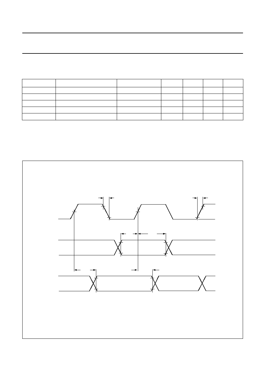
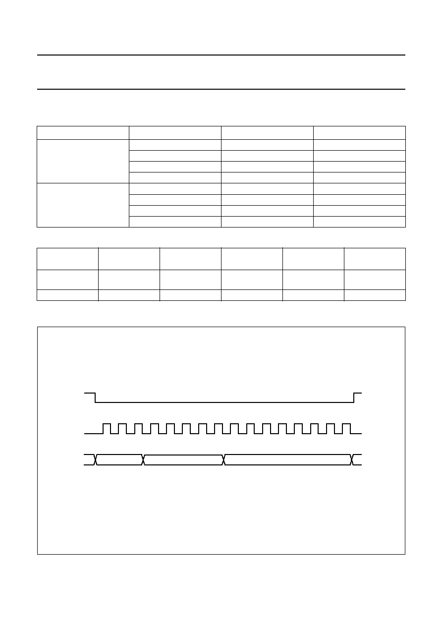
AC CHARACTERISTICS
Microprocessor interface
V
DD
= 2.7 to 3.3 V; V
IL
= 0 V; V
IH
= V
DD
; V
ref
= 0.5V
DD
; T
amb
=
-
20 to +70
∞
C; input t
r
and t
f
= 30 ns; unless otherwise
specified.
SYMBOL
PARAMETER
MIN.
TYP.
MAX.
UNIT
t
CSs
CS set-up time
0.4
-
-
µ
s
t
CSh
CS hold time
0.4
-
-
µ
s
t
CSd
CS deselection time
0.2
-
-
µ
s
t
Ds
DI set-up time
0.4
-
-
µ
s
t
Dh
DI hold time
0.4
-
-
µ
s
f
CK
CK frequency
-
-
0.5
MHz
t
WCKH
HIGH level pulse width of CK
1.0
-
-
µ
s
t
WCKL
LOW level pulse width of CK
1.0
-
-
µ
s
t
r
rise time of CK
-
-
100
ns
t
f
fall time of CK
-
-
100
ns
Fig.3 Microprocessor interface timing.
CS
CK
DI
tCSs
tr
tf
MHA305
tCSd
Vref
Vref
Vref
VIH
VIH
VIH
VIL
VIL
VIL
tCSh
tWCKH
90%
90%
10%
10%
tDs
tDh
tWCKL
1996 Feb 16
10
Philips Semiconductors
Preliminary specification
Camera Digital Signal Processor
(CAMDSP)
SAA9750H
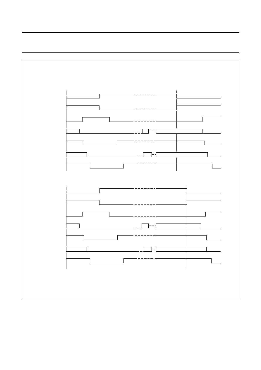
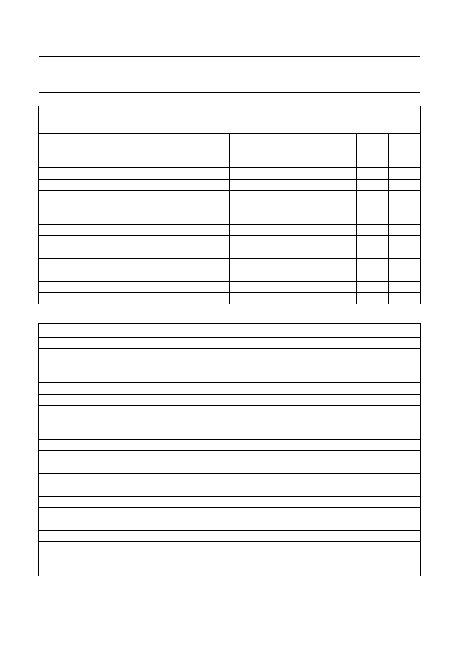
Data input/output timing (CLK1 and CLK2)
V
DD
= 2.7 to 3.3 V; V
IL
= 0 V; V
IH
= V
DD
; V
ref
= 0.5V
DD
;T
amb
=
-
20 to +70
∞
C; t
r
and t
f
= 6 ns; output load
capacitance = 20 pF; unless otherwise specified.
Notes
1. Data inputs: SYNCI, CPOB, CDS
0
to CDS
8
, VRST, HRST, R, G, B, TSW, Y
ENC0
to Y
ENC7
, LSW and
UV
ENC0
to UV
ENC7
.
2. Data outputs: UV
SEL
, UV
0
to UV
7
, Y
0
to Y
7
, WCLIP, CSYNC, HSYNC, FLD, HD, VD and CP2.
3. T
amb
= +25
∞
C; V
DD
= 3.0 V.
SYMBOL
PARAMETER
CONDITIONS
MIN.
TYP.
MAX.
UNIT
t
DIs
data input set-up time
note 1
5
-
-
ns
t
DIh
data input hold time
note 1
8
-
-
ns
t
DOd
data output delay time
notes 2 and 3
-
-
50
ns
t
DOh
data output hold time
notes 2 and 3
-
-
50
ns
t
duty
duty factor of CLK1 and CLK2
-
50
-
%
Fig.4 Data input/output timing (CLK1 and CLK2).
CLK1 and
CLK2
data inputs
data outputs
tf
MHA306
tr
Vref
VIH
VIH
VOH
VIL
VIL
VOL
90%
10%
90%
10%
90%
10%
90%
10%
90%
10%
90%
10%
tDIs
tDOd
tDIh
tDOh

1996 Feb 16
11
Philips Semiconductors
Preliminary specification
Camera Digital Signal Processor
(CAMDSP)
SAA9750H
SSG TIMING
Clock count for NTSC and PAL mode
Fig.5 SSG timing (continued in Fig.6).
handbook, full pagewidth
,,
,,
,,
,,
,,,,,
,,,,,
,,,
,,,
,
,
,,,,,,
,,,,,,
,,,
,,,,,,
,,
,,,,,,,
CCD 510H
1H
606 (618) clocks
596 (603)
1H
806 (824) clocks
0
50 (45)
60 (60)
24 (24)
33 (33)
48 (48)
57 (57)
62 (62)
80 (80)
80 (80)
32 (32)
28 (28)
48 (48)
51 (51)
61 (61)
100 (100)
108 (108)
121 (121)
MHA307
168 (184)
195 (203)
107 (107)
165 (177)
93 (93)
139 (151)
75 (75)
CCD 670H
0
SHD
HD
CP2
Y0 to Y7
HSYNC
YDA and CDA
SYNC
SHD
HD
CP2
Y0 to Y7
HSYNC
YDA and CDA
SYNC
-
10 (
-
15)
1996 Feb 16
12
Philips Semiconductors
Preliminary specification
Camera Digital Signal Processor
(CAMDSP)
SAA9750H
SHD: HD output can be changed by microprocessor to SHD outputs.
HD: For timing of input CDS signal for PPG IC.
HSYNC: For output luminance signal Y7 to Y0 and chrominance signal UV7 to UV0 of CAMDSPs YC processing.
SYNC: Composite SYNC pulse of DACs output.
Output of CSYNC (pin 59): SYNC + 1 clock (see Figs 5 and 6).
Fig.6 SSG timing (continued from Fig.5).
handbook, full pagewidth
,,,
,,,,,
,,,
,,
,,
,,,,,
,,,
,,,
,,
,,
,,,,,
,,,,,
,,,
,,,
,,
,,
,,,,,
,,,,,
CCD 720H
1H
858 (864) clocks
1H
910 (908) clocks
0
83 (83)
83 (83)
36 (36)
34 (34)
50 (50)
63 (63)
67 (67)
89 (89)
89 (89)
36 (36)
33 (33)
54 (54)
65 (63)
71 (71)
108 (108)
121 (121)
138 (138)
MHA308
191 (203)
223 (235)
130 (130)
209 (229)
113 (113)
172 (182)
104 (104)
CCD 768H
0
SHD
HD
CP2
Y0 to Y7
HSYNC
YDA and CDA
SYNC
SHD
HD
CP2
Y0 to Y7
HSYNC
YDA and CDA
SYNC
1996 Feb 16
13
Philips Semiconductors
Preliminary specification
Camera Digital Signal Processor
(CAMDSP)
SAA9750H
Clock
Table 1
Clock frequency
Table 2
Clock used for each block
MICROPROCESSOR INTERFACE FORMAT
MODE
CCD
CLK1 (MHz)
CLK2 (MHz)
NTSC
510H
9.5350
19.0699
670H
12.7132
-
720H
13.5000
-
768H
14.3182
-
PAL
SECAM
510H
9.6563
19.3125
670H
12.8750
-
720H
13.5000
-
768H
14.1875
-
MODE
SSG BLOCK
Y/C BLOCK
ENCODER
BLOCK
Y-DAC BLOCK
C-DAC BLOCK
510H NTSC/PAL
CLK1
CLK1
CLK1 and CLK2
(upsampling)
CLK1
CLK2
Other modes
CLK1
CLK1
CLK1
CLK1
CLK1
Fig.7 Microprocessor interface format.
(1) Slave address 001.
handbook, full pagewidth
CS
CK
DI
MSB
LSB
MSB
LSB
MSB
LSB
data
subaddress
slave address
(1)
MHA304

1996 Feb 16
14
Philips Semiconductors
Preliminary specification
Camera Digital Signal Processor
(CAMDSP)
SAA9750H
Table 3
Microprocessor interface format
FUNCTION
SUBADDRESS
DATA
MSB
LSB
Field delay
00000
X
-
-
-
-
-
-
FD
Title enable
00000
X
-
-
-
-
-
TE
-
Title polarity
00000
X
-
-
-
-
TP
-
-
False colour +6 dB
00000
X
-
-
-
FCU
-
-
-
UV +6 dB
00000
X
-
-
CUP
-
-
-
-
Y +6 dB
00000
X
-
YUP
-
-
-
-
-
Y clear
00000
X
YCL
-
-
-
-
-
-
HAP LOW clip
00001
X
X
HA5
HA4
HA3
HA2
HA1
HA0
VAP LOW clip
00010
X
X
VA5
VA4
VA3
VA2
VA1
VA0
AP HIGH clip
00011
X
-
-
-
AP3
AP2
AP1
AP0
AP gain
00011
X
AG2
AG1
AG0
-
-
-
-
Y gain
00100
X
X
YG5
YG4
YG3
YG2
YG1
YG0
Y pedestal
00101
YP7
YP6
YP5
YP4
YP3
YP2
YP1
YP0
Slice
00110
X
X
X
-
-
-
SLI
SNP
Mosaic
00110
X
X
X
MOS
PX1
PX0
-
-
Slice level
00111
SLL7
SLL6
SLL5
SLL4
SLL3
SLL2
SLL1
SLL0
Subcarrier
01000
S7
S6
S5
S4
S3
S2
S1
S0
01001
S15
S14
S13
S12
S11
S10
S9
S8
01010
-
-
-
-
S19
S18
S17
S16
UV polarity
01010
-
-
-
UVP
-
-
-
-
SYNCI
01010
-
-
SYN
-
-
-
-
-
Encoder mode
01010
EM1
EM0
-
-
-
-
-
-
Burst level
01011
X
BL6
BL5
BL4
BL3
BL2
BL1
BL0
HRST delay
01101
D7
D6
D5
D4
D3
D2
D1
D0
01110
-
-
-
-
-
-
D9
D8
CCD type
01110
-
-
-
-
H1
H0
-
-
525/625 line
01110
-
-
-
LL
-
-
-
-
Master/slave
01110
-
-
MS
-
-
-
-
-
ADC delay
01110
AD1
AD0
-
-
-
-
-
-
Solarization
01111
X
X
X
-
-
-
TR1
TR0
01111
X
X
X
-
-
SOL
-
-
Sepia
01111
X
X
X
-
SEP
-
-
-
Negative/positive
01111
X
X
X
NP
-
-
-
-
R gain
10000
X
RG6
RG5
RG4
RG3
RG2
RG1
RG0
B gain
10001
X
BG6
BG5
BG4
BG3
BG2
BG1
BG0
U gain
10010
X
X
UGP5
UGP4
UGP3
UGP2
UGP1
UGP0
10011
X
X
UGN5
UGN4
UGN3
UGN2
UGN1
UGN0
1996 Feb 16
15
Philips Semiconductors
Preliminary specification
Camera Digital Signal Processor
(CAMDSP)
SAA9750H
Table 4
Explanation of functions of Table 3
V gain
10100
X
X
VGP5
VGP4
VGP3
VGP2
VGP1
VGP0
10101
X
X
VGN5
VGN4
VGN3
VGN2
VGN1
VGN0
U matrix 1 gain
10110
X
X
UM5
UM4
UM3
UM2
UM1
UM0
U matrix 2 gain
10111
X
X
UN5
UN4
UN3
UN2
UN1
UN0
V matrix 1 gain
11000
X
X
VM5
VM4
VM3
VM2
VM1
VM0
V matrix 2 gain
11001
X
X
VN5
VN4
VN3
VN2
VN1
VN0
SP polarity
11010
X
X
X
-
-
-
-
SPP
FH2 polarity
11010
X
X
X
-
-
-
FHP
-
Colour filter
11010
X
X
X
-
-
LPF
-
-
HD, VD polarity
11010
X
X
X
-
SHV
-
-
-
Sub LPF
11010
X
X
X
JGM
-
-
-
-
False colour
11011
TH7
TH6
TH5
TH4
TH3
TH2
TH1
TH0
White-clip level
11100
WC7
WC6
WC5
WC4
WC3
WC2
WC1
WC0
Y delay
11101
X
X
X
X
-
-
YDL1
YDL0
C delay
11101
X
X
X
X
CDL1
CDL0
-
-
SYMBOL
DESCRIPTION
FD
field delay control
TE
title enable control
TP
title polarity control
FCU
false colour plus 6 dB up
CUP
UV +6 dB up
YUP
Y gain +6 dB up
YCL
Y clear control
HA0 to HA5
horizontal aperture LOW clip level control
VA0 to VA5
vertical aperture LOW clip level control
AP0 to AP3
aperture HIGH clip level control
AG0 to AG2
aperture gain control
YG0 to YG5
Y gain control
YP0 to YP7
Y pedestal control
SNP
slice effect polarity
SLI
slice ON/OFF
PX0 and PX1
mosaic effect pixels control
MOS
mosaic ON/OFF
SLL0 to SLL7
slice level control
S0 to S19
subcarrier control
UVP
UV
SEL
polarity control
SYN
SYNC signal selection
FUNCTION
SUBADDRESS
DATA
MSB
LSB

1996 Feb 16
16
Philips Semiconductors
Preliminary specification
Camera Digital Signal Processor
(CAMDSP)
SAA9750H
EM0 and EM1
encoder mode control
BL0 to BL6
burst level control
D0 to D9
HRST and VRST preset control
H0 and H1
CCD type selection
LL
525/625 line control
MS
master/slave control
AD0 and AD1
ADC delay control
TR0 and TR1
solarization effect control
SOL
solarization ON/OFF
SEP
sepia ON/OFF
NP
negative/positive ON/OFF
RG0 to RG6
red gain control
BG0 to BG6
blue gain control
UGP0 to UGP5
U gain control for positive side
UGN0 to UGN5
U gain control for negative side
VGP0 to VGP5
V gain control for positive side
VGN0 to VGN5
V gain control for negative side
UM0 to UM5
U matrix 1 gain control
UN0 to UN5
U matrix 2 gain control
VM0 to VM5
V matrix 1 gain control
VN0 to VN5
V matrix 2 gain control
SPP
SP polarity control
FHP
FH2 polarity control
LPF
colour filter control
SHV
HD and VD polarity control
JGM
sub LPF control for false colour
TH0 to TH7
threshold control for false colour suppression
WC0 to WC7
white-clip level control
YDL0 and YDL1
Y delay control
CDL0 and CDL1
C delay control
SYMBOL
DESCRIPTION
1996 Feb 16
17
Philips Semiconductors
Preliminary specification
Camera Digital Signal Processor
(CAMDSP)
SAA9750H
MICROPROCESSOR SETTING
Table 5
Field delay control
Table 6
Title enable control
Table 7
Title polarity control
Table 8
False colour +6 dB up
Table 9
UV +6 dB up
Table 10 Y gain +6 dB up
Table 11 Y clear control
FIELD DELAY CONTROL
FD
Normal
0
One field delay
1
TITLE ENABLE CONTROL
TE
Title insertion OFF
0
Title insertion ON
1
TITLE POLARITY CONTROL
TP
Negative
0
Positive
1
FALSE COLOUR +6 dB UP
FCU
0 dB gain
0
+6 dB gain
1
UV +6 dB UP
CUP
0 dB gain
0
+6 dB gain
1
Y GAIN +6 dB UP
YUP
0 dB gain
0
+6 dB gain
1
Y CLEAR CONTROL
YCL
Normal
0
Clear
1
Horizontal aperture LOW clip level control = HA5 to HA0.
Vertical aperture LOW clip level control = VA5 to VA0.
Aperture HIGH clip level control = AP3 to AP0.
Aperture gain control
Y gain control
Y pedestal level control = YP7 to YP0.
Table 12 Slice effect polarity
Table 13 Slice ON/OFF
Table 14 Mosaic effect pixels control
Table 15 Mosaic ON/OFF
Slice level control = SLL7 to SLL0.
Subcarrier frequency control
SLICE EFFECT POLARITY
SNP
Negative
0
Positive
1
SLICE ON/OFF
SLI
OFF normal
0
ON slice
1
MOSAIC EFFECT PIXELS CONTROL
PX1
PX0
4
◊
4 pixels
0
0
8
◊
8 pixels
0
1
16
◊
16 pixels
1
0
32
◊
32 pixels
1
1
MOSAIC ON/OFF
MOS
OFF normal
0
ON mosaic
1
AG 2:0
[
]
8
------------------------
=
YG 5:0
[
]
32
-------------------------
=
S 19:0
[
]
f
encoder
◊
1048576
-------------------------------------------------
=
1996 Feb 16
18
Philips Semiconductors
Preliminary specification
Camera Digital Signal Processor
(CAMDSP)
SAA9750H
Table 16 UV
SEL
polarity control
Table 17 SYNC signal selection
Table 18 Encoder mode control
Burst level control
(of full-scale DAC output).
HRST and VRST preset control = D9 to D0, preset
horizontal counter to count D9 to D0.
Table 19 CCD type selection
Table 20 525/625 line control
UV
SEL
POLARITY
CONTROL
UVP
Normal
0 HIGH: U(B
-
Y) LOW: V(R
-
Y)
Invert
1 HIGH: V(R
-
Y) LOW: U(B
-
Y)
SYNC SIGNAL SELECTION
SYN
Internal SYNC
0
External SYNC (from SYNCI pin 60)
1
ENCODER MODE CONTROL
EM1
EM0
PAL
0
0
NTSC
0
1
SECAM
1
0
Bypass
1
1
CCD TYPE SELECTION
H1
H0
510H
0
0
670H
0
1
720H
1
0
768H
1
1
525/625 LINE CONTROL
LL
525 line
0
625 line
1
BL 6:0
[
]
128
-----------------------
=
Table 21 Master/slave control
Table 22 AD converter delay control
Table 23 Solarization effect control
Table 24 Solarization ON/OFF
Table 25 Sepia ON/OFF
Table 26 Negative/positive ON/OFF
MASTER/SLAVE CONTROL
MS
Master
0
Slave
1
ADC DELAY CONTROL
(CAMDSP DELAY)
AD1
AD0
3Ts
0
0
4Ts
0
1
5Ts
1
0
6Ts
1
1
SOLARIZATION EFFECT CONTROL
(SLICE OF BITS)
TR1
TR0
3 bits (LSB)
0
0
4 bits (LSB)
0
1
5 bits (LSB)
1
0
6 bits (LSB)
1
1
SOLARIZATION ON/OFF
SOL
Normal
0
Solarization ON
1
SEPIA ON/OFF
SEP
Normal
0
Sepia ON
1
NEGATIVE/POSITIVE ON/OFF
NP
Normal
1
Negative
0

1996 Feb 16
19
Philips Semiconductors
Preliminary specification
Camera Digital Signal Processor
(CAMDSP)
SAA9750H
R channel gain control = 1 +
(1)
B channel gain control = 1 +
(1)
U gain control for positive side
U gain control for negative side
V gain control for positive side
V gain control for negative side
U matrix 1 gain control
(1)
U matrix 2 gain control
(1)
V matrix 1 gain control
(1)
V matrix 2 gain control
(1)
Table 27 SP polarity control
Table 28 FH2 polarity control
(1) RG, BG, UM, UN, VM and VN are twos complement.
SP POLARITY CONTROL
SPP
Normal
0
H: Ye + Mg or Ye + Gr
L: Cy + Gr or Cy + Mg
Invert
1
H: Cy + Gr or Cy + Mg
L: Ye + Mg or Ye + Gr
FH2 POLARITY CONTROL
FHP
Normal
0
H: 2B-G
L: 2R-G
Invert
1
H: 2R-G
L: 2B-G
RG 6:0
[
]
128
-------------------------
BG 6:0
[
]
128
------------------------
UGP 5:0
[
]
16
-----------------------------
=
UGN 5:0
[
]
16
-----------------------------
=
VGP 5:0
[
]
16
-----------------------------
=
VGN 5:0
[
]
16
-----------------------------
=
UM 5:0
[
]
32
-------------------------
=
UN 5:0
[
]
32
------------------------
=
VM 5:0
[
]
32
-------------------------
=
VN 5:0
[
]
32
------------------------
=
Table 29 Colour filter control
Table 30 HD and VD polarity control
Table 31 Sub LPF control for false colour
Threshold control for false colour suppress = TH7 to TH0.
White clip level control = 2
◊
WC7 to WC0.
Table 32 Y delay control
Table 33 C delay control
COLOUR FILTER
CONTROL
LPF
LPF1
0
[1,1,3,3,4,4,4,4,3,3,1,1]/32
LPF2
1
[
-
1,0,4,8,10,8,4,0,
-
1]/32
HD AND VD POLARITY CONTROL
SHV
Normal
0
Invert
1
SUB LPF CONTROL FOR FALSE COLOUR
JGM
Normal
0
Sub LPF
1
Y DELAY CONTROL
YDL1
YDL0
0 clock period
0
0
+1 clock period
0
1
+2 clock periods
1
0
+3 clock periods
1
1
C DELAY CONTROL
CDL1
CDL0
0 clock period
0
0
+1 clock period
0
1
+2 clock periods
1
0
+3 clock periods
1
1
1996
Feb
16
20
Philips Semiconductors
Preliminary specification
Camera Digital Signal Processor
(CAMDSP)
SAA9750H
CAMERA
Fig.8 Camera block diagram (SAA9750H and SAA9740H).
handbook, full pagewidth
CAMDSP
SIGNAL
PROCESSOR
Y/C SEPARATION
SSG
ENCODER
SAA9750H
ADC
IRIS
DRIVER
DAC
PPG
iris
AGC
CCD
high speed
shuffle control
LPF
CAMERA
ADC
I/F(8)
CDS(8)
UV(8)
Y(5)
BPF
Y
MHA303
C
Y (8-bit)
UV (8-bit)
CDS
AGC, GAMMA
CLAMP
HD/VD
8-bit
SAA9750H
MICRO-
PROCESSOR
serial
data bus
A2CF
AF/AE/AWB
UVSEL
HSYNC
WCLIP
MOTOR
DRIVER
focus
lens
MOTOR
DRIVER
zoom
lens
hall
sensor
focus
sensor
zoom
encoder
3
1996 Feb 16
21
Philips Semiconductors
Preliminary specification
Camera Digital Signal Processor
(CAMDSP)
SAA9750H
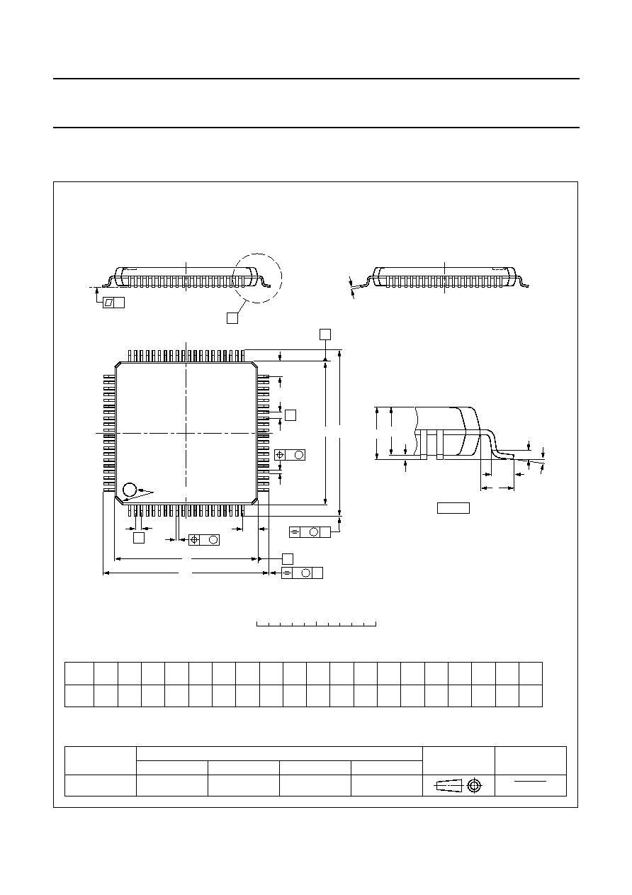
PACKAGE OUTLINE
UNIT
A
max.
A
1
A
2
A
3
b
p
c
E
(1)
e
H
E
L
L
p
Z
y
w
v
REFERENCES
OUTLINE
VERSION
EUROPEAN
PROJECTION
ISSUE DATE
IEC
JEDEC
EIAJ
mm
1.6
0.16
0.04
1.5
1.3
0.25
0.27
0.13
0.18
0.12
12.1
11.9
0.5
14.15
13.85
1.45
1.05
7
0
o
o
0.15
0.1
0.2
1.0
DIMENSIONS (mm are the original dimensions)
Note
1. Plastic or metal protrusions of 0.25 mm maximum per side are not included.
0.75
0.30
SOT315-1
97-07-15
95-12-19
D
(1)
(1)
(1)
12.1
11.9
H
D
14.15
13.85
E
Z
1.45
1.05
D
b
p
e
E
A
1
A
L
p
detail X
L
(A )
3
B
20
c
D
H
b
p
E
H
A
2
v
M
B
D
Z D
A
Z E
e
v
M
A
X
1
80
61
60
41
40
21
y
pin 1 index
w
M
w
M
0
5
10 mm
scale
LQFP80: plastic low profile quad flat package; 80 leads; body 12 x 12 x 1.4 mm
SOT315-1

1996 Feb 16
22
Philips Semiconductors
Preliminary specification
Camera Digital Signal Processor
(CAMDSP)
SAA9750H
SOLDERING
Introduction
There is no soldering method that is ideal for all IC
packages. Wave soldering is often preferred when
through-hole and surface mounted components are mixed
on one printed-circuit board. However, wave soldering is
not always suitable for surface mounted ICs, or for
printed-circuits with high population densities. In these
situations reflow soldering is often used.
This text gives a very brief insight to a complex technology.
A more in-depth account of soldering ICs can be found in
our
"IC Package Databook" (order code 9398 652 90011).
Reflow soldering
Reflow soldering techniques are suitable for all LQFP
packages.
Reflow soldering requires solder paste (a suspension of
fine solder particles, flux and binding agent) to be applied
to the printed-circuit board by screen printing, stencilling or
pressure-syringe dispensing before package placement.
Several techniques exist for reflowing; for example,
thermal conduction by heated belt. Dwell times vary
between 50 and 300 seconds depending on heating
method. Typical reflow temperatures range from
215 to 250
∞
C.
Preheating is necessary to dry the paste and evaporate
the binding agent. Preheating duration: 45 minutes at
45
∞
C.
Wave soldering
Wave soldering is not recommended for LQFP packages.
This is because of the likelihood of solder bridging due to
closely-spaced leads and the possibility of incomplete
solder penetration in multi-lead devices.
If wave soldering cannot be avoided, the following
conditions must be observed:
∑
A double-wave (a turbulent wave with high upward
pressure followed by a smooth laminar wave)
soldering technique should be used.
∑
The footprint must be at an angle of 45
∞
to the board
direction and must incorporate solder thieves
downstream and at the side corners.
Even with these conditions, do not consider wave
soldering LQFP packages LQFP48 (SOT313-2),
LQFP64 (SOT314-2) or LQFP80 (SOT315-1).
During placement and before soldering, the package must
be fixed with a droplet of adhesive. The adhesive can be
applied by screen printing, pin transfer or syringe
dispensing. The package can be soldered after the
adhesive is cured.
Maximum permissible solder temperature is 260
∞
C, and
maximum duration of package immersion in solder is
10 seconds, if cooled to less than 150
∞
C within
6 seconds. Typical dwell time is 4 seconds at 250
∞
C.
A mildly-activated flux will eliminate the need for removal
of corrosive residues in most applications.
Repairing soldered joints
Fix the component by first soldering two diagonally-
opposite end leads. Use only a low voltage soldering iron
(less than 24 V) applied to the flat part of the lead. Contact
time must be limited to 10 seconds at up to 300
∞
C. When
using a dedicated tool, all other leads can be soldered in
one operation within 2 to 5 seconds between
270 and 320
∞
C.

1996 Feb 16
23
Philips Semiconductors
Preliminary specification
Camera Digital Signal Processor
(CAMDSP)
SAA9750H
DEFINITIONS
LIFE SUPPORT APPLICATIONS
These products are not designed for use in life support appliances, devices, or systems where malfunction of these
products can reasonably be expected to result in personal injury. Philips customers using or selling these products for
use in such applications do so at their own risk and agree to fully indemnify Philips for any damages resulting from such
improper use or sale.
Data sheet status
Objective specification
This data sheet contains target or goal specifications for product development.
Preliminary specification
This data sheet contains preliminary data; supplementary data may be published later.
Product specification
This data sheet contains final product specifications.
Limiting values
Limiting values given are in accordance with the Absolute Maximum Rating System (IEC 134). Stress above one or
more of the limiting values may cause permanent damage to the device. These are stress ratings only and operation
of the device at these or at any other conditions above those given in the Characteristics sections of the specification
is not implied. Exposure to limiting values for extended periods may affect device reliability.
Application information
Where application information is given, it is advisory and does not form part of the specification.

Philips Semiconductors ≠ a worldwide company
Argentina: IEROD, Av. Juramento 1992 - 14.b, (1428)
BUENOS AIRES, Tel. (541)786 7633, Fax. (541)786 9367
Australia: 34 Waterloo Road, NORTH RYDE, NSW 2113,
Tel. (02)805 4455, Fax. (02)805 4466
Austria: Triester Str. 64, A-1101 WIEN, P.O. Box 213,
Tel. (01)60 101-1236, Fax. (01)60 101-1211
Belgium: Postbus 90050, 5600 PB EINDHOVEN, The Netherlands,
Tel. (31)40-2783749, Fax. (31)40-2788399
Brazil: Rua do Rocio 220 - 5
th
floor, Suite 51,
CEP: 04552-903-S√O PAULO-SP, Brazil,
P.O. Box 7383 (01064-970),
Tel. (011)821-2333, Fax. (011)829-1849
Canada: PHILIPS SEMICONDUCTORS/COMPONENTS:
Tel. (800) 234-7381, Fax. (708) 296-8556
Chile: Av. Santa Maria 0760, SANTIAGO,
Tel. (02)773 816, Fax. (02)777 6730
China/Hong Kong: 501 Hong Kong Industrial Technology Centre,
72 Tat Chee Avenue, Kowloon Tong, HONG KONG,
Tel. (852)2319 7888, Fax. (852)2319 7700
Colombia: IPRELENSO LTDA, Carrera 21 No. 56-17,
77621 BOGOTA, Tel. (571)249 7624/(571)217 4609,
Fax. (571)217 4549
Denmark: Prags Boulevard 80, PB 1919, DK-2300
COPENHAGEN S, Tel. (45)32 88 26 36, Fax. (45)31 57 19 49
Finland: Sinikalliontie 3, FIN-02630 ESPOO,
Tel. (358)0-615 800, Fax. (358)0-61580 920
France: 4 Rue du Port-aux-Vins, BP317,
92156 SURESNES Cedex,
Tel. (01)4099 6161, Fax. (01)4099 6427
Germany: P.O. Box 10 51 40, 20035 HAMBURG,
Tel. (040)23 53 60, Fax. (040)23 53 63 00
Greece: No. 15, 25th March Street, GR 17778 TAVROS,
Tel. (01)4894 339/4894 911, Fax. (01)4814 240
India: Philips INDIA Ltd, Shivsagar Estate, A Block,
Dr. Annie Besant Rd. Worli, Bombay 400 018
Tel. (022)4938 541, Fax. (022)4938 722
Indonesia: Philips House, Jalan H.R. Rasuna Said Kav. 3-4,
P.O. Box 4252, JAKARTA 12950,
Tel. (021)5201 122, Fax. (021)5205 189
Ireland: Newstead, Clonskeagh, DUBLIN 14,
Tel. (01)7640 000, Fax. (01)7640 200
Italy: PHILIPS SEMICONDUCTORS S.r.l.,
Piazza IV Novembre 3, 20124 MILANO,
Tel. (0039)2 6752 2531, Fax. (0039)2 6752 2557
Japan: Philips Bldg 13-37, Kohnan 2 -chome, Minato-ku, TOKYO 108,
Tel. (03)3740 5130, Fax. (03)3740 5077
Korea: Philips House, 260-199 Itaewon-dong,
Yongsan-ku, SEOUL, Tel. (02)709-1412, Fax. (02)709-1415
Malaysia: No. 76 Jalan Universiti, 46200 PETALING JAYA,
SELANGOR, Tel. (03)750 5214, Fax. (03)757 4880
Mexico: 5900 Gateway East, Suite 200, EL PASO, TX 79905,
Tel. 9-5(800)234-7381, Fax. (708)296-8556
Netherlands: Postbus 90050, 5600 PB EINDHOVEN, Bldg. VB,
Tel. (040)2783749, Fax. (040)2788399
New Zealand: 2 Wagener Place, C.P.O. Box 1041, AUCKLAND,
Tel. (09)849-4160, Fax. (09)849-7811
Norway: Box 1, Manglerud 0612, OSLO,
Tel. (022)74 8000, Fax. (022)74 8341
Pakistan: Philips Electrical Industries of Pakistan Ltd.,
Exchange Bldg. ST-2/A, Block 9, KDA Scheme 5, Clifton,
KARACHI 75600, Tel. (021)587 4641-49,
Fax. (021)577035/5874546
Philippines: PHILIPS SEMICONDUCTORS PHILIPPINES Inc.,
106 Valero St. Salcedo Village, P.O. Box 2108 MCC, MAKATI,
Metro MANILA, Tel. (63) 2 816 6380, Fax. (63) 2 817 3474
Portugal: PHILIPS PORTUGUESA, S.A.,
Rua dr. AntÛnio Loureiro Borges 5, Arquiparque - Miraflores,
Apartado 300, 2795 LINDA-A-VELHA,
Tel. (01)4163160/4163333, Fax. (01)4163174/4163366
Singapore: Lorong 1, Toa Payoh, SINGAPORE 1231,
Tel. (65)350 2000, Fax. (65)251 6500
South Africa: S.A. PHILIPS Pty Ltd.,
195-215 Main Road Martindale, 2092 JOHANNESBURG,
P.O. Box 7430, Johannesburg 2000,
Tel. (011)470-5911, Fax. (011)470-5494
Spain: Balmes 22, 08007 BARCELONA,
Tel. (03)301 6312, Fax. (03)301 42 43
Sweden: Kottbygatan 7, Akalla. S-164 85 STOCKHOLM,
Tel. (0)8-632 2000, Fax. (0)8-632 2745
Switzerland: Allmendstrasse 140, CH-8027 ZÐRICH,
Tel. (01)488 2211, Fax. (01)481 77 30
Taiwan: PHILIPS TAIWAN Ltd., 23-30F, 66, Chung Hsiao West
Road, Sec. 1. Taipeh, Taiwan ROC, P.O. Box 22978,
TAIPEI 100, Tel. (886) 2 382 4443, Fax. (886) 2 382 4444
Thailand: PHILIPS ELECTRONICS (THAILAND) Ltd.,
209/2 Sanpavuth-Bangna Road Prakanong,
Bangkok 10260, THAILAND,
Tel. (66) 2 745-4090, Fax. (66) 2 398-0793
Turkey: Talatpasa Cad. No. 5, 80640 GÐLTEPE/ISTANBUL,
Tel. (0 212)279 27 70, Fax. (0212)282 67 07
Ukraine: Philips UKRAINE, 2A Akademika Koroleva str., Office 165,
252148 KIEV, Tel. 380-44-4760297, Fax. 380-44-4766991
United Kingdom: Philips Semiconductors LTD.,
276 Bath Road, Hayes, MIDDLESEX UB3 5BX,
Tel. (0181)730-5000, Fax. (0181)754-8421
United States: 811 East Arques Avenue, SUNNYVALE,
CA 94088-3409, Tel. (800)234-7381, Fax. (708)296-8556
Uruguay: Coronel Mora 433, MONTEVIDEO,
Tel. (02)70-4044, Fax. (02)92 0601
Internet: http://www.semiconductors.philips.com/ps/
For all other countries apply to: Philips Semiconductors,
International Marketing and Sales, Building BE-p,
P.O. Box 218, 5600 MD EINDHOVEN, The Netherlands,
Telex 35000 phtcnl, Fax. +31-40-2724825
SCDS47
© Philips Electronics N.V. 1996
All rights are reserved. Reproduction in whole or in part is prohibited without the
prior written consent of the copyright owner.
The information presented in this document does not form part of any quotation
or contract, is believed to be accurate and reliable and may be changed without
notice. No liability will be accepted by the publisher for any consequence of its
use. Publication thereof does not convey nor imply any license under patent- or
other industrial or intellectual property rights.
Printed in The Netherlands
537021/1100/01/pp24
Date of release: 1996 Feb 16
Document order number:
9397 750 00641