 | –≠–ª–µ–∫—Ç—Ä–æ–Ω–Ω—ã–π –∫–æ–º–ø–æ–Ω–µ–Ω—Ç: SAB9079 | –°–∫–∞—á–∞—Ç—å:  PDF PDF  ZIP ZIP |

DATA SHEET
Preliminary specification
File under Integrated Circuits, IC02
2000 Jan 13
INTEGRATED CIRCUITS
SAB9079HS
Multistandard Picture-In-Picture
(PIP) controller

2000 Jan 13
2
Philips Semiconductors
Preliminary specification
Multistandard Picture-In-Picture (PIP)
controller
SAB9079HS
FEATURES
∑
Suitable for single PIP, double window and multi PIP
applications
∑
Data formats 4 : 1 : 1 (all modes) and 4 : 2 : 2 (most
modes)
∑
Sample rate of 14 MHz, 720 Y*-pixels/line
∑
Horizontal reduction factors
1
/
1
3
/
4
,
2
/
3
,
1
/
2
,
1
/
3
,
1
/
4
and
1
/
6
∑
Vertical reduction factors
1
/
1
,
1
/
2
,
1
/
3
and
1
/
4
∑
PIP OSD for the sub channels displayed
∑
Detection of PAL/NTSC with overrule bit
∑
CTE/LTE like circuits in display part
∑
Replay with definable auto increment, picture sample
rate and picture number auto wrap
∑
Programmable Y*UV to RGB conversion matrix with
independent coefficients for NTSC and PAL sources
∑
Display clock and synchronisation are derived from the
main PLL
∑
Three 8-bit Digital-to-Analog Converters (DACs)
∑
Three 8-bit Analog-to-Digital Converters (ADCs)
(7-bit performance) with clamp circuit for each
acquisition channel
∑
Main and sub can write to the same VDRAM address
spaces under certain conditions; the reduction factors
should be the same
∑
Y* and UV pedestals on the acquisition sides
∑
Independent vertical filtering with 1 : 1 for UV and Y* at
the display part.
GENERAL DESCRIPTION
The SAB9079HS is a PIP controller for a multistandard
application environment in combination with a
multistandard decoder such as for example TDA8310,
TDA9143 or TDA9321H.
The SAB9079HS inserts one or two live video signals with
reduced sizes into the main/display video signal. All video
signals are expected to be analog baseband signals. The
analog signals are stripped signals without sync.
Therefore the luminance signal is referred to as Y*. The
conversion into the digital environment and back is done
on-chip as well as the internal clock generation.
The SAB9079HS is suitable for single PIP, double window
and multi PIP applications.
ORDERING INFORMATION
TYPE
NUMBER
PACKAGE
NAME
DESCRIPTION
VERSION
SAB9079HS
SQFP128
plastic shrink quad flat package; 128 leads (lead length 1.6 mm);
body 14
◊
20
◊
2.72 mm
SOT387-3

2000 Jan 13
3
Philips Semiconductors
Preliminary specification
Multistandard Picture-In-Picture (PIP)
controller
SAB9079HS
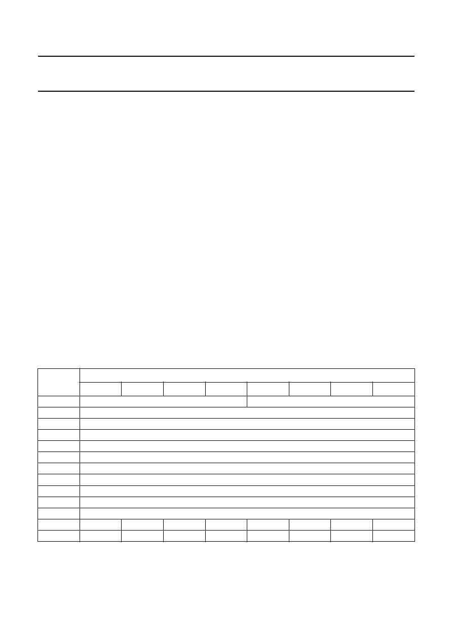
QUICK REFERENCE DATA
SYMBOL
PARAMETER
CONDITIONS
MIN.
TYP.
MAX.
UNIT
Supplies
V
DDD(C)
digital supply voltage for the core
3.0
3.3
3.6
V
V
DDD(P)
digital supply voltage for the
periphery
4.5
5.0
5.5
V
V
DDA
analog supply voltage
3.0
3.3
3.6
V
I
DDD(C)
digital supply current for the core
tbf
115
tbf
mA
I
DDD(P)
digital supply current for the
periphery
tbf
10
tbf
mA
I
DDA
analog supply current
-
170
210
mA
PLL
f
osc
oscillator frequency
3584
◊
HSYNC
-
56
-
MHz
f
sys
system frequency
1792
◊
HSYNC
-
28
-
MHz
896
◊
HSYNC
-
14
-
MHz
448
◊
HSYNC
-
7
-
MHz
B
loop
loop bandwidth
-
4
-
kHz
t
jitter
short term stability
jitter during 64
µ
s
-
-
4
ns
damping factor
-
0.7
-

2000
Jan
13
4
Philips Semiconductors
Preliminar
y specification
Multistandard Picture-In-Picture (PIP)
controller
SAB9079HS
This text is here in white to force landscape pages to be rotated correctly when browsing through the pdf in the Acrobat reader.This text is here in
_
white to force landscape pages to be rotated correctly when browsing through the pdf in the Acrobat reader.This text is here inThis text is here in
white to force landscape pages to be rotated correctly when browsing through the pdf in the Acrobat reader. white to force landscape pages to be ...
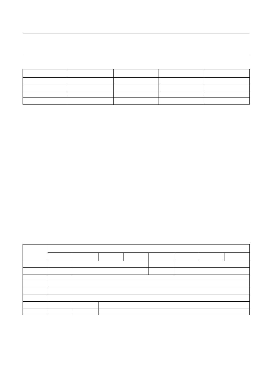
BLOCK DIA
GRAM
handbook, full pagewidth
MGS386
SAB9079HS
I
2
C-BUS
CONTROL
CLAMP AND ADC
VDRAM CONTROL
AND
(RE-)FORMATTING
SY
105
SU
103
SV
101
PLL AND CLOCK
GENERATOR
Vbias(SA)
104
Vref(T)(SA)
107
Vref(B)(SA)
106
CLAMP AND ADC
MY
126
MU
128
MV
2
PLL AND CLOCK
GENERATOR
PLL AND CLOCK
GENERATOR
HORIZONTAL
AND
VERTICAL
FILTER
LINE MEMORY
HORIZONTAL
AND
VERTICAL
FILTER
DAC
AND
BUFFER
DISPLAY
CONTROL
LINE MEMORY
LINE MEMORY
TEST
CONTROL
MHSYNC
9
DVSYNC
MVSYNC
21
n.c.
84
DFB
19
Vref(T)(DA)
25
Vref(B)(DA)
26
Vbias(DA)
28
DV
29
DU
27
DY
24
DHSYNC
20
8
SHSYNC
94
SVSYNC
95
Vbias(MA)
127
Vref(T)(MA)
124
125
Vref(B)(MA)
111
114
TCBR
A0
110
115
TCBD
SDA
97
112
116
TCBC
SCL
117
TSMSB
POR
121
TM0
120
TM2
119
TM1
118
TC
7
TMCLK
15, 18, 22,
85, 88,
109, 122
VDDD(C1)
to
VDDD(C7)
16, 17, 23,
86, 87,
108, 123
VSSD(C1)
to
VSSD(C7)
13,
47, 63,
75, 90
VSSD(P1)
to
VSSD(P5)
14,
48, 62,
76, 89
VDDD(P1)
to
VDDD(P5)
98
TSEXT
78
70
77
40
51
SC
79 to 83,
74 to 71
AD8
to AD0
41 to 46,
49, 50, 69,
67, 65, 61,
59, 57, 55, 53
DAO0
to DAO15
39 to 32,
68, 66, 64,
60, 58, 56,
54, 52
DAI0
to DAI15
30
VSSA(DA)
31
VDDA(DA)
113
VDDD(P)
1
VDDA(MF)
3
VSSA(MA)
4
VDDA(MA)
10
VDDA(MP)
11
VSSA(MP)
12
VDDA(MH)
99
VDDA(SA)
100
VSSA(SA)
102
VDDA(SF)
91
VDDA(SH)
92
VSSA(SP)
93
VDDA(SP)
6
TMMSB
5
TMEXT
96
TSCLK
CAS
WE
RAS
DT
Fig.1 Block diagram.

2000 Jan 13
5
Philips Semiconductors
Preliminary specification
Multistandard Picture-In-Picture (PIP)
controller
SAB9079HS
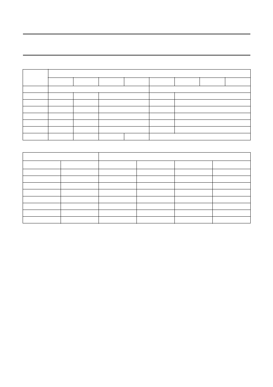
PINNING
SYMBOL
PIN
I/O
DESCRIPTION
V
DDA(MF)
1
S
analog supply voltage for main channel front-end (3.3 V)
MV
2
I
analog V input of main channel
V
SSA(MA)
3
S
analog ground for main channel ADCs
V
DDA(MA)
4
S
analog supply voltage for main channel ADCs (3.3 V)
TMEXT
5
I
set main PLL input for external mode (CMOS levels)
TMMSB
6
O
test main MSB output of PLL counter (CMOS levels)
TMCLK
7
I
test clock main input (CMOS levels)
MVSYNC
8
I
vertical sync input for main channel (CMOS levels with hysteresis)
MHSYNC
9
I
horizontal sync input for main channel (CMOS levels with hysteresis)
V
DDA(MP)
10
S
analog supply voltage for main channel PLL (3.3 V)
V
SSA(MP)
11
S
analog ground for main channel PLL
V
DDA(MH)
12
S
supply of main HSYNC input (5.0 V)
V
SSD(P1)
13
S
digital ground 1 for periphery; note 1
V
DDD(P1)
14
S
digital supply voltage 1 for periphery (5.0 V); note 2
V
DDD(C1)
15
S
digital supply voltage 1 for core (3.3 V); note 3
V
SSD(C1)
16
S
digital ground 1 for core; note 4
V
SSD(C2)
17
S
digital ground 2 for core; note 4
V
DDD(C2)
18
S
digital supply voltage 2 for core (3.3 V); note 3
DFB
19
O
fast blanking control output (CMOS levels)
DHSYNC
20
O
horizontal sync output (CMOS levels)
DVSYNC
21
O
vertical sync output (CMOS levels)
V
DDD(C3)
22
S
digital supply voltage 3 for core (3.3 V); note 3
V
SSD(C3)
23
S
digital ground 3 for core; note 4
DY
24
O
analog Y* output of DAC
V
ref(T)(DA)
25
I/O
analog top reference for DACs
V
ref(B)(DA)
26
I/O
analog bottom reference for DACs
DU
27
O
analog U output of DAC
V
bias(DA)
28
I/O
analog voltage reference DACs
DV
29
O
analog V output of DAC
V
SSA(DA)
30
S
analog ground for DACs
V
DDA(DA)
31
S
analog supply voltage for DACs (3.3 V)
DAI7
32
I
memory input data bit 7 (CMOS levels)
DAI6
33
I
memory input data bit 6 (CMOS levels)
DAI5
34
I
memory input data bit 5 (CMOS levels)
DAI4
35
I
memory input data bit 4 (CMOS levels)
DAI3
36
I
memory input data bit 3 (CMOS levels)
DAI2
37
I
memory input data bit 2 (CMOS levels)
DAI1
38
I
memory input data bit 1 (CMOS levels)
DAI0
39
I
memory input data bit 0 (CMOS levels)
DT
40
O
memory data transfer (CMOS levels)

2000 Jan 13
6
Philips Semiconductors
Preliminary specification
Multistandard Picture-In-Picture (PIP)
controller
SAB9079HS
DAO0
41
O
memory output data bit 0 (CMOS levels)
DAO1
42
O
memory output data bit 1 (CMOS levels)
DAO2
43
O
memory output data bit 2 (CMOS levels)
DAO3
44
O
memory output data bit 3 (CMOS levels)
DAO4
45
O
memory output data bit 4 (CMOS levels)
DAO5
46
O
memory output data bit 5 (CMOS levels)
V
SSD(P2)
47
S
digital ground 2 for periphery; note 1
V
DDD(P2)
48
S
digital supply voltage 2 for periphery (5.0 V); note 2
DAO6
49
O
memory output data bit 6 (CMOS levels)
DAO7
50
O
memory output data bit 7 (CMOS levels)
SC
51
O
memory shift clock output (CMOS levels)
DAI15
52
I
memory input data bit 15 (CMOS levels)
DAO15
53
O
memory output data bit 15 (CMOS levels)
DAI14
54
I
memory input data bit 14 (CMOS levels)
DAO14
55
O
memory output data bit 14 (CMOS levels)
DAI13
56
I
memory input data bit 13 (CMOS levels)
DAO13
57
O
memory output data bit 13 (CMOS levels)
DAI12
58
I
memory input data bit 12 (CMOS levels)
DAO12
59
O
memory output data bit 12 (CMOS levels)
DAI11
60
I
memory input data bit 11 (CMOS levels)
DAO11
61
O
memory output data bit 11 (CMOS levels)
V
DDD(P3)
62
S
digital supply voltage 3 for periphery (5.0 V); note 2
V
SSD(P3)
63
S
digital ground 3 for periphery; note 1
DAI10
64
I
memory input data bit 10 (CMOS levels)
DAO10
65
O
memory output data bit 10 (CMOS levels)
DAI9
66
I
memory input data bit 9 (CMOS levels)
DAO9
67
O
memory output data bit 9 (CMOS levels)
DAI8
68
I
memory input data bit 8 (CMOS levels)
DAO8
69
O
memory output data bit 8 (CMOS levels)
CAS
70
O
memory column address strobe output (CMOS levels)
AD0
71
O
memory address output bit 0 (CMOS levels)
AD1
72
O
memory address output bit 1 (CMOS levels)
AD2
73
O
memory address output bit 2 (CMOS levels)
AD3
74
O
memory address output bit 3 (CMOS levels)
V
SSD(P4)
75
S
digital ground 4 for periphery; note 1
V
DDD(P4)
76
S
digital supply voltage 4 for periphery (5.0 V); note 2
WE
77
O
memory write enable output (CMOS levels)
RAS
78
O
memory row address strobe output (CMOS levels)
AD8
79
O
memory address output bit 8 (CMOS levels)
AD7
80
O
memory address output bit 7 (CMOS levels)
AD6
81
O
memory address output bit 6 (CMOS levels)
SYMBOL
PIN
I/O
DESCRIPTION

2000 Jan 13
7
Philips Semiconductors
Preliminary specification
Multistandard Picture-In-Picture (PIP)
controller
SAB9079HS
AD5
82
O
memory address output bit 5 (CMOS levels)
AD4
83
O
memory address output bit 4 (CMOS levels)
n.c.
84
-
not used in application
V
DDD(C4)
85
S
digital supply voltage 4 for core (3.3 V); note 3
V
SSD(C4)
86
S
digital ground 4 for core; note 4
V
SSD(C5)
87
S
digital ground 5 for core; note 4
V
DDD(C5)
88
S
digital supply voltage 5 for core (3.3 V); note 3
V
DDD(P5)
89
S
digital supply voltage 5 for periphery (5.0 V); note 2
V
SSD(P5)
90
S
digital ground 5 for periphery; note 1
V
DDA(SH)
91
S
supply of sub HSYNC input (5.0 V)
V
SSA(SP)
92
S
analog ground for sub channel PLL
V
DDA(SP)
93
S
analog supply voltage for sub channel PLL (3.3 V)
SHSYNC
94
I
horizontal sync input for sub channel (CMOS levels with hysteresis)
SVSYNC
95
I
vertical sync input for sub channel (CMOS levels with hysteresis)
TSCLK
96
I
test clock input for sub (CMOS levels)
TSMSB
97
O
test sub MSB output for PLL counter (CMOS levels)
TSEXT
98
I
set sub PLL input for external mode (CMOS levels)
V
DDA(SA)
99
S
analog supply voltage for sub channel ADCs (3.3 V)
V
SSA(SA)
100
S
analog ground for sub channel ADCs
SV
101
I
analog V input of sub channel
V
DDA(SF)
102
S
analog supply voltage for sub channel frontend (3.3 V)
SU
103
I
analog U input of sub channel
V
bias(SA)
104
I/O
analog bias reference input for sub channel ADCs
SY
105
I
analog Y* input of sub channel
V
ref(B)(SA)
106
I/O
analog bottom reference for sub channel ADCs
V
ref(T)(SA)
107
I/O
analog top reference for sub channel ADCs
V
SSD(C6)
108
S
digital ground 6 for core; note 4
V
DDD(C6)
109
S
digital supply voltage 6 for core (3.3 V); note 3
TCBC
110
I
test control block clock input (CMOS levels)
TCBD
111
I
test control block data input (CMOS levels)
TCBR
112
I
test control block reset input (CMOS levels)
V
DDD(P)
113
S
digital supply voltage for periphery (5.0 V); note 5
A0
114
I
address select pin input (I
2
C-bus) (CMOS levels)
SDA
115
I/O
serial input data/ACK output (I
2
C-bus) (CMOS input levels)
SCL
116
I
serial clock input (I
2
C-bus) (CMOS levels)
POR
117
I
power-on reset input (CMOS levels with hysteresis and pull-up resistor to V
DD
)
TC
118
I
test control input (CMOS levels)
TM1
119
I/O
test mode input/output (CMOS levels with hysteresis and pull-up resistor to V
DD
)
TM2
120
I/O
test mode input/output (CMOS levels with hysteresis and pull-up resistor to V
DD
)
TM0
121
I
test mode input (CMOS levels)
V
DDD(C7)
122
S
digital supply voltage 7 for core (3.3 V); note 3
SYMBOL
PIN
I/O
DESCRIPTION

2000 Jan 13
8
Philips Semiconductors
Preliminary specification
Multistandard Picture-In-Picture (PIP)
controller
SAB9079HS
Notes
1. All periphery V
SS(P)
are internally connected to each other, unless otherwise specified.
2. All periphery V
DD(P)
are internally connected to each other, unless otherwise specified.
3. All core V
DD(C)
are internally connected to each other.
4. All core V
SS(C)
are internally connected to each other.
5. This pin is NOT connected to the other periphery V
DD(P)
.
V
SSD(C7)
123
S
digital ground 7 for core; note 4
V
ref(T)(MA)
124
I/O
analog top reference for main channel ADCs
V
ref(B)(MA)
125
I/O
analog bottom reference for main channel ADCs
MY
126
I
analog Y* input for main channel
V
bias(MA)
127
I/O
analog bias reference for main channel ADCs
MU
128
I
analog U input for main channel
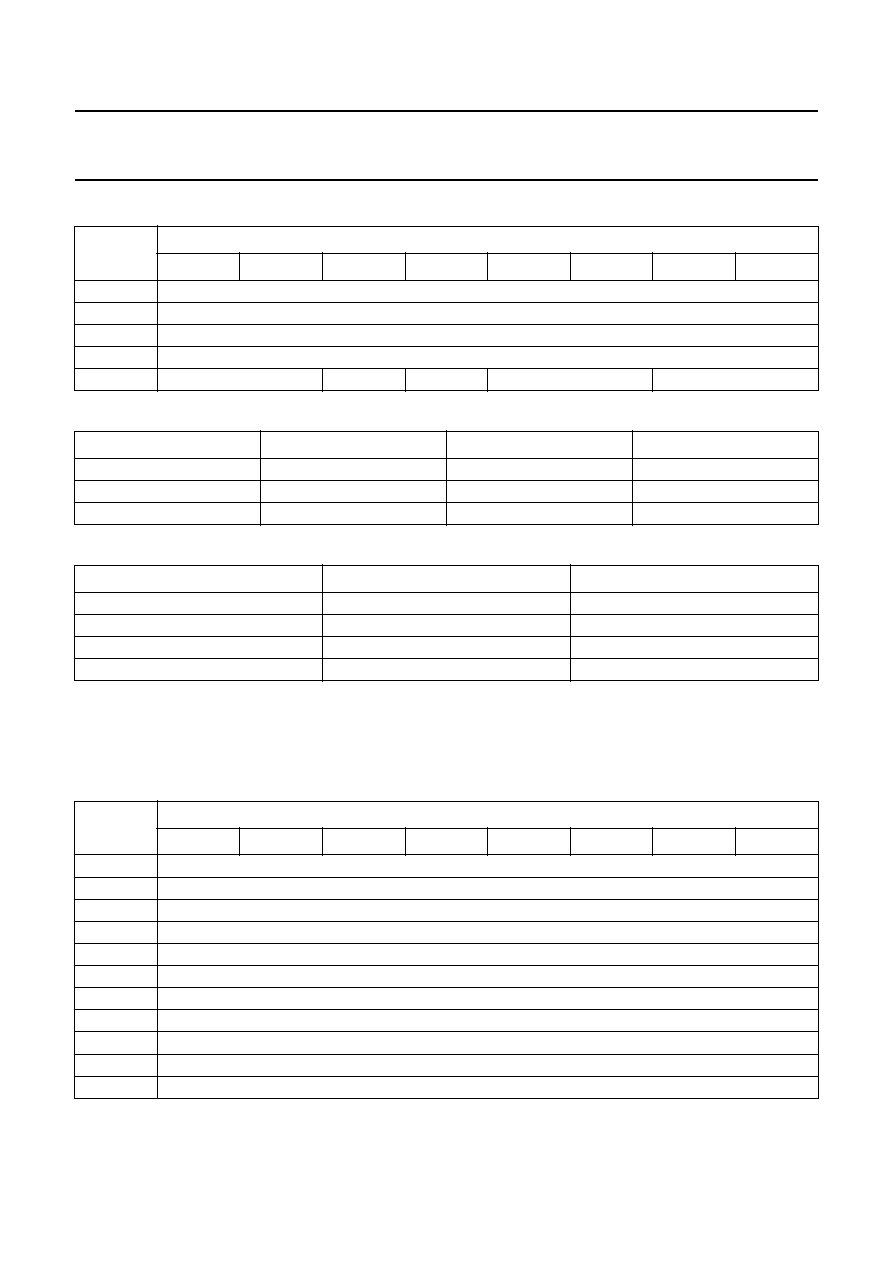
SYMBOL
PIN
I/O
DESCRIPTION
2000 Jan 13
9
Philips Semiconductors
Preliminary specification
Multistandard Picture-In-Picture (PIP)
controller
SAB9079HS
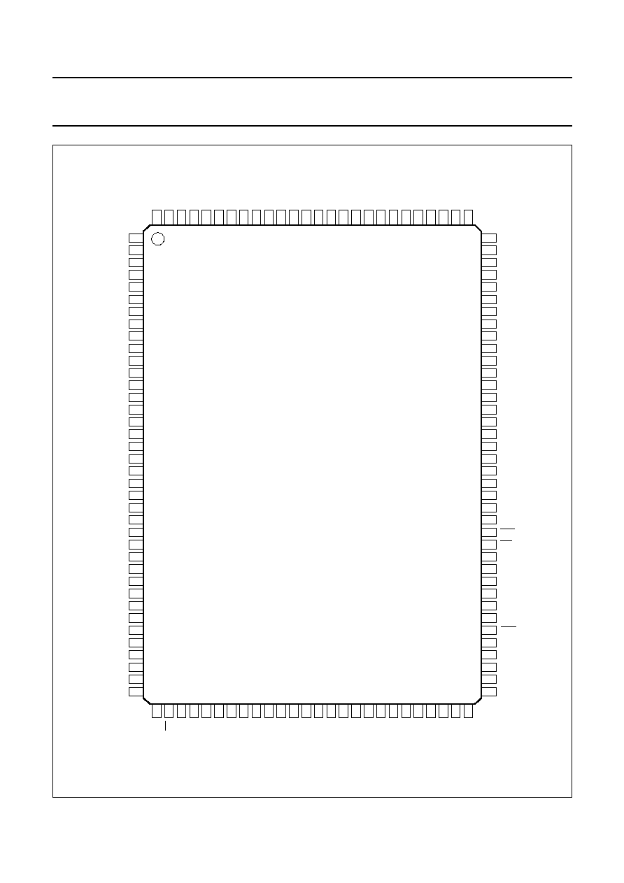
Fig.2 Pin configuration.
handbook, full pagewidth
MGS387
SAB9079HS
2
1
3
4
5
6
7
8
9
10
11
12
13
14
15
16
17
18
19
20
21
22
23
24
25
26
27
28
29
30
31
32
33
34
35
36
37
38
101
102
100
99
98
97
96
95
94
93
92
91
90
89
88
87
86
85
84
83
82
81
80
79
78
77
76
75
74
73
72
71
70
69
68
67
66
65
SV
VDDA(SF)
VSSA(SA)
VDDA(SA)
TSEXT
TSMSB
TSCLK
SVSYNC
SHSYNC
VDDA(SP)
VSSA(SP)
VDDA(SH)
VSSD(P5)
VDDD(P5)
VDDD(C5)
VSSD(C5)
VSSD(C4)
VDDD(C4)
n.c.
AD4
AD5
AD6
AD7
AD8
VDDD(P4)
VSSD(P4)
AD3
AD2
AD1
AD0
DAO8
DAI8
DAO9
DAI9
DAO10
MV
VDDA(MF)
VSSA(MA)
VDDA(MA)
TMEXT
TMMSB
TMCLK
MVSYNC
MHSYNC
VDDA(MP)
VSSA(MP)
VDDA(MH)
VSSD(P1)
VDDD(P1)
VDDD(C1)
VSSD(C1)
VSSD(C2)
VDDD(C2)
DFB
DHSYNC
DVSYNC
VDDD(C3)
VSSD(C3)
DY
Vref(T)(DA)
Vref(B)(DA)
DU
Vbias(DA)
DV
VSSA(DA)
VDDA(DA)
DAI7
DAI6
DAI5
DAI4
DAI3
DAI2
DAI1
40
39
41
42
43
44
45
46
47
48
49
50
51
52
53
54
55
56
57
58
59
60
61
62
63
64
127
128
126
125
124
123
122
121
120
119
118
117
116
115
114
113
112
111
110
109
108
107
106
105
104
103
V
bias(MA)
MU
MY
V
ref(B)(MA)
V
ref(T)(MA)
V
SSD(C7)
V
DDD(C7)
TM0
TM2
TM1
TC
POR
SCL
SDA
A0
V
DDD(P)
TCBR
TCBD
TCBC
V
DDD(C6)
V
SSD(C6)
V
ref(T)(SA
)
V
ref(B)(SA
)
SY
V
bias(SA
)
SU
DAI0
DAO0
DAO1
DAO2
DAO3
DAO4
DAO5
V
SSD(P2)
V
DDD(P2)
DAO6
DAO7
SC
DAI15
DAO15
DAI14
DAO14
DAI13
DAO13
DAI12
DAO12
DAI11
DAO11
V
DDD(P3)
V
SSD(P3)
DAI10
DT
CAS
WE
RAS
2000 Jan 13
10
Philips Semiconductors
Preliminary specification
Multistandard Picture-In-Picture (PIP)
controller
SAB9079HS
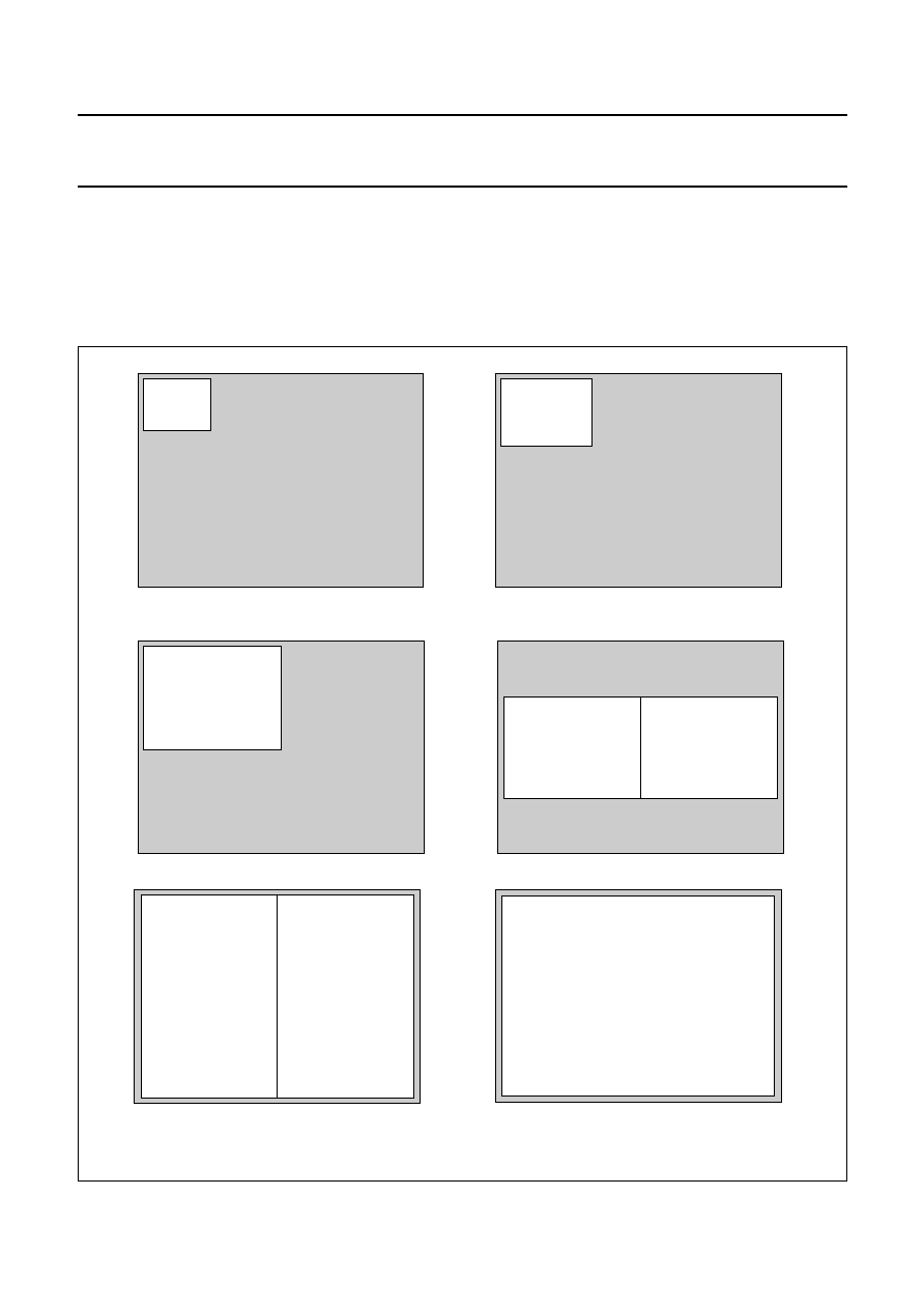
SYSTEM DESCRIPTION
PIP modes
An overview of the general PIP modes is given in Figs 3, 4 and 5. These pictures do not refer to all possible modes the
device can handle. These modes are guaranteed only when sufficient memory is available and enough time is available
to fetch all data from the memory.
Fig.3 PIP modes.
handbook, halfpage
MGD594
SP-Small
handbook, halfpage
MGD595
SP-Medium
handbook, halfpage
MGD596
SP-Large
handbook, halfpage
MGD597
DP
handbook, halfpage
MGD598
Twin-PIP
handbook, halfpage
MGD587
Full Field Still
Full Field Live
2000 Jan 13
11
Philips Semiconductors
Preliminary specification
Multistandard Picture-In-Picture (PIP)
controller
SAB9079HS
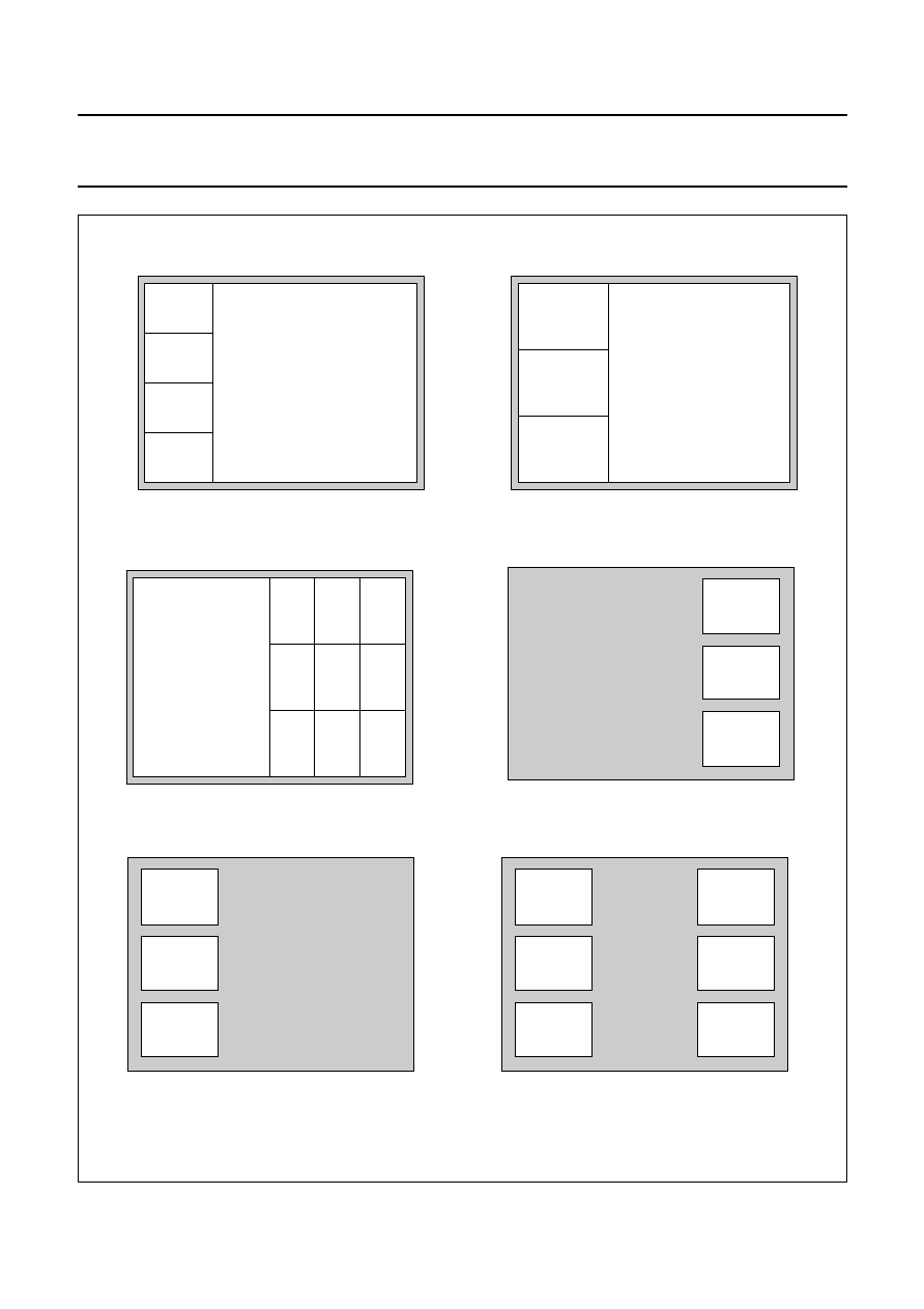
Fig.4 PIP modes (continued).
handbook, halfpage
MGD589
POP-Right
handbook, halfpage
MGD588
POP-Left
handbook, halfpage
MGD590
POP-Double
handbook, halfpage
MGS388
handbook, halfpage
MGS389
handbook, halfpage
MGS390

2000 Jan 13
12
Philips Semiconductors
Preliminary specification
Multistandard Picture-In-Picture (PIP)
controller
SAB9079HS
handbook, halfpage
MGL925
MP13
Fig.5 PIP modes (continued).
handbook, halfpage
MGD591
MP7
handbook, halfpage
MGD592
MP8
handbook, halfpage
MGD584
Quatro
handbook, halfpage
MGD585
MP9
handbook, halfpage
MGD586
MP16

2000 Jan 13
13
Philips Semiconductors
Preliminary specification
Multistandard Picture-In-Picture (PIP)
controller
SAB9079HS
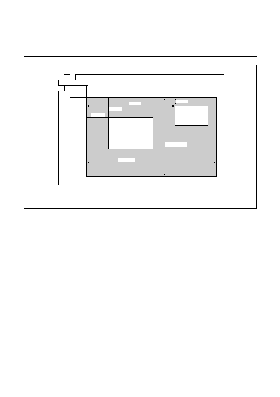
Acquisition window
The acquisition window is 720 pixels. This is related to a
whole line of 896 pixels. So for PAL
will be
acquired from the active video. For NTSC this will be
slightly less
.
The vertical acquisition window is 228 lines for NTSC and
276 lines for PAL. Data will be acquired in a 4 : 2 : 2
format. The acquisition clock is 896
◊
HSYNC.
Acquisition fine positioning
All I
2
C-bus settings relate to the incoming HSYNC,
whether this is a real HSYNC or a burstkey for horizontal
positioning. The same applys for the incoming VSYNC for
vertical positioning. The relationships between the
acquisition window and the internal clamp pulse are
illustrated in Fig.6. In an application the clamp pulse must
be positioned, by the I
2
C-bus, between the HSYNC and
the start of the active video of the incoming signal.
Display window
The display window available for PIP pictures is also
720 pixels wide, related to a 896 pixels line. The vertical
display window is 228 lines for NTSC and 276 lines for
PAL.
Background window
The origin of the display window is referenced to the origin
of the background window. The background area is
768 pixels wide. Vertically it is 238 lines for NTSC and
286 lines for PAL.
Display fine positioning
The I
2
C-bus defined fine positioning has relationships to
the internal HSYNC and VSYNC as illustrated in Fig.7.
720
896
----------
64
µ
s
◊
720
896
----------
63.5
µ
s
◊
Fig.6 Acquisition fine positioning.
handbook, full pagewidth
MGS391
MAHFP
MAVFP
CIDEL
CIPER
228/276 lines
720 pixels
The grey area depicts the background.
2000 Jan 13
14
Philips Semiconductors
Preliminary specification
Multistandard Picture-In-Picture (PIP)
controller
SAB9079HS
Fig.7 Display fine positioning.
handbook, full pagewidth
MGS392
BGHFP
BGVFP
MAIN CHANNEL
SUB CHANNEL
SDHFP
MDVFP
MDHFP
SDVFP
238/286 lines
768 pixels
The grey area depicts the background.
YUV to RGB conversion matrix
A YUV to RGB conversion matrix is available. The nine
matrix coefficient values can be set by I
2
C-bus commands.
Two sets can be defined; one for PAL and one for NTSC.
The matrix must be switched on, otherwise a 1 : 1
conversion takes place and Y*, U and V will be
unmodified.
The conversion matrix is based on the following equations.
All results (R, G and B) fall in the range from 0 to 1. Any
results outside of this range will be clipped to the nearest
end value. It should be noted that gamma correction is not
applied as is common practice. The end of this section
contains an example.
Normalised Y, U and V (indicated by subscript `a') are
given by the following four equations:
1. Y
a
= x
◊
R
a
+ y
◊
G
a
+ z
◊
B
a
2. x + y + z = 1
3. U
a
= B
a
-
Y
a
4. V
a
= R
a
-
Y
a
Absolute or discrete (indicated by subscript `d') values
for Y, U and V are given by the following three equations:
1. Y
d
= 255
◊
Y
a
(V), Y
a
normalised (range 0 to 1)
2.
,
U
a
normalised (range
-
1 to +1)
3.
,
V
a
normalised (range
-
1 to +1)
U
d
128
127
U
a
1
z
≠
------------
◊
+
=
V
d
128
127
V
a
1
x
≠
------------
◊
+
=
2000 Jan 13
15
Philips Semiconductors
Preliminary specification
Multistandard Picture-In-Picture (PIP)
controller
SAB9079HS
Absolute or discrete (indicated by subscript `d') values for R, G and B are given by the following three equations:
1.
2.
3.
The implementation of a matrix with 9 coefficients is shown in Table 1.
Table 1
Matrix coefficients
So, for example;
R = ry
◊
Y
d
+ ru
◊
2
◊
(U
d
-
128) + rv
◊
2
◊
(V
d
-
128)
Table 2 shows how the coefficients can be calculated for a specific case where x = 0.299, y = 0.587 and z = 0.114.
Calculation of xv:y* 128 (rounded to the nearest integer), translates to a binary value. Calculation of xu:xv: translates to
a binary value with the coefficients for the binary bits:
-
1,
1
/
2
1
/
4
,
1
/
8
,
1
/
16
,
1
/
32
,
1
/
64
1
/
128
(LSB).
Table 2
Coefficient calculation
YUV TO RGB MATRIX
COEFFICIENTS
Y
d
U
d
V
d
COFACTOR: Y
d
COFACTOR: 2
◊
(U
d
-
128) COFACTOR: 2
◊
(V
d
-
128)
R
ry = 1
ru = 0
G
gy = 1
B
by = 1
bv = 0
COEFFICIENT
EXPRESSION
DECIMAL VALUE
BINARY VALUE
ry
1
1
10000000
ru
0
0
00000000
rv
0.704
01011010
gy
1
1
10000000
gu
-
0.173
11101010
gv
-
0.358
11010010
by
1
1
10000000
bu
0.889
01110010
bv
0
0
00000000
R
d
Y
d
255
127
----------
V
d
128
≠
(
)
1
x
≠
(
)
◊
◊
+
=
G
d
Y
d
255
127
----------
x
y
---
1
x
≠
(
)
◊
V
d
128
≠
(
)
◊
◊
≠
255
127
----------
z
y
---
1
z
≠
(
)
◊
U
d
128
≠
(
)
◊
◊
≠
=
B
d
Y
d
255
127
----------
U
d
128
≠
(
)
1
z
≠
(
)
◊
◊
+
=
rv
255
254
----------
1
x
≠
(
)
◊
=
gu
255
254
----------
z
y
---
1
z
≠
(
)
◊
◊
≠
=
gv
255
254
----------
x
y
---
◊
1
x
≠
(
)
◊
≠
=
bu
255
254
----------
1
z
≠
(
)
◊
=
255
254
----------
1
x
≠
(
)
◊
255
254
----------
z
y
---
◊
1
z
≠
(
)
◊
≠
255
254
----------
x
y
---
◊
1
x
≠
(
)
◊
≠
255
254
----------
1
z
≠
(
)
◊
2000 Jan 13
16
Philips Semiconductors
Preliminary specification
Multistandard Picture-In-Picture (PIP)
controller
SAB9079HS
PLL phase shift compensation for VCR
When a VCR is applied as source for the main channel, a
large phase jump can appear when the VCR head
switches to another field. Since this phenomenon occurs
around the VSYNC, its effects can be compensated.
A prediction mechanism generates a compensation
window around the VSYNC. This window can be
manipulated with two parameters; VsPre and VsPost.
∑
VsPre sets the number of lines before the predicted
VSYNC, where the compensation window will start
∑
VsPost sets the number of lines after the actual VSYNC,
where the compensation window will end.
I
2
C-bus
I
2
C-
BUS CONTROL
The SAB9079HS is a slave receiver/transmitter. The
protocols are given in Tables 3 and 5.
Table 3
I
2
C-bus slave receiver protocol
Table 4
Description of Table 3
Table 5
I
2
C-bus slave transmitter protocol
Table 6
Description of Table 5
S
SLAVE
A
SUB
A
DATA
A
DATA
A
P
SYMBOL
DESCRIPTION
S
START condition
A
acknowledge bit (generated by SAB9079HS)
P
STOP condition
SLAVE
slave address; the data transmission starts with the slave address byte SLV (2CH or 2EH);
the LSB of the SLV byte is the R/W bit which is logic 0 in slave receiver mode
SUB
sub address byte; the SUB byte indicates the sub address which has to be written; if more than
one data byte is send (as above) the internal sub address counter is automatically incremented
after each data byte
DATA
data byte; the data byte is the actual data written to the sub address; the functions of each sub
address are explained in the following Sections
S
SLAVE
A
DATA
A
DATA
A
DATA
N
P
SYMBOL
DESCRIPTION
S
START condition
A
acknowledge bit; after the SLV generated by the SAB9079HS; after the DATA generated by the
master
N
acknowledge not bit; given by the master after the last data byte
P
STOP condition
SLAVE
slave address; the data transmission starts with the slave address byte SLV (2DH or 2FH);
the LSB of the SLV byte is the R/W bit which is logic 1 in slave transmitter mode
DATA
data byte; this is put on the bus by SAB9079HS in an auto increment mode; if the master gives an
acknowledge the next data byte is sent; if the SAB9079HS has sent all its data it starts again with
the first data byte and the sequence is repeated; this continues until an acknowledge not is given
by the master
2000 Jan 13
17
Philips Semiconductors
Preliminary specification
Multistandard Picture-In-Picture (PIP)
controller
SAB9079HS
The SAB9079HS has 8 read/status registers. The last 7 registers are reserved for future purposes. Reading a reserved
register will return zero values.
The SAB9079HS has 192 write registers. Writing to a reserved register is not allowed.
An overview of all write registers is given in Table 7.
Table 7
Description of write registers
I
2
C-
BUS READ REGISTERS
The SAB9079HS has 8 read/status registers. The register currently used are listed in Table 8. The remaining 7 are
reserved for future purposes. Reading a reserved register will return zero values.
Table 8
I
2
C-bus read registers
SUB ADDRESS RANGE
PURPOSE
00H to 04H
display
05H to 11H
positioning and sizing of PIPs
12H to 17H
decoder settings
18H to 1FH
acquisition control
20H to 25H
decoder and PLL settings
26H to 28H
reserved
29H to 2AH
decoder and PLL settings
2BH to 2FH
replay settings
30H to 37H
border and colour settings
38H to 3CH
OSD controls
3DH to 4EH
YUV to RGB conversion matrix settings
4FH to 5FH
extra decoder settings
60H to 7FH
reserved
80H to DFH
OSD characters
E0H to FFH
reserved
SUB
ADDRESS
DATA BYTES
BIT 7
BIT 6
BIT 5
BIT 4
BIT 3
BIT 2
BIT 1
BIT 0
00H
SNonInt
Mask ID
RepChano
01H
reserved
02H
reserved
03H
reserved
04H
reserved
05H
reserved
06H
reserved
07H
reserved

2000 Jan 13
18
Philips Semiconductors
Preliminary specification
Multistandard Picture-In-Picture (PIP)
controller
SAB9079HS
SNonInt
This bit indicates the internal interface status of the sub
channel. A logic 0 indicates that the channel is in
interlaced mode, a logic 1 indicates that the channel is
non-interlaced.
Mask ID
This bit gives the version number of the chip. A logic 0
indicates that a SAB9079N1 is used, a logic 1 indicates
that a SAB9079N2 is used.
RepChano
These bits indicate the present picture number, counting
from 0, where replay acquisition is writing.
I
2
C-
BUS DISPLAY SETTING REGISTERS
MPIPON and SPIPON
If MPIPON is set to logic 1 (see Table 10) the main PIP is
on. If it is set to logic 0 the main PIP is off. If SPIPON is set
to logic 1 the sub PIPs are on, in accordance with the
scheme of the PIPG bits (see Section "Positioning and
sizing of PIPs"). If SPIPON is set to logic 0 all the sub PIPs
are off. This can also be achieved by setting all PIPG bits
to zero.
MFreeze and SFreeze
MFreeze and SFreeze control the writing of data to the
VDRAM. If set to logic 0 the writing to the VDRAM is
disabled after the next VSYNC. If set to logic 1 the writing
is enabled after the next VSYNC.
I
2
CHold
The I
2
C-bus hold bit is set to logic 0 (default). This means
that all I
2
C-bus data is directly clocked into the internal
registers. A part of the I
2
C-bus data will be clocked in on
the next VSYNC (e.g. the reduction factors and the display
positioning). If the I
2
CHold bit is logic 1 that part of the
I
2
C-bus will not be clocked in on the next VSYNC. To make
the data available the I
2
CHold bit should be set to logic 0
again. This function is useful when much data has to be
sent and a screen update is not allowed when sending this
data. A list of I
2
C-bus registers which are clocked in on a
VSYNC is given below:
∑
MPIPON and SPIPON
∑
MFreeze, SFreeze and FillSet
∑
DNonInt, MNonInt and SNonInt
∑
PRIO
∑
BGHfp, BGVfp, MDHfp, MDVfp, SDHfp and SDVfp
∑
MHPic, MVPic, SHPic, SVPic, SHDis and SVDis
∑
PIPG
c,r
∑
MHRed, MVRed, SHRed, SVRed, MLSel,
SLSel and SBSel
∑
OSDHfp, OSDVfp, OSDHDis and OSDVDis.
FillSet and FillOff
The FillSet bit sets the colour of all sub PIPs immediately
to a 30% grey value if is set to logic 1. If FillSet is set to
logic 0 then the 30% grey PIPs stay until the data in the
VDRAM is updated (unfrozen). This bit should be used in
the event that a new PIP mode is made in which the
VDRAM data becomes invalid. FillOff works the opposite
to FillSet. If this bit is set all the VDRAM data is made
visible in the PIPs and no PIP has a grey content. This bit
is generally not used.
MiS
If the MiS bit is set to logic 0 the main and sub channels
have their own independent memory spaces. If set to
logic 1 the main and sub channels share the same
memory space, this is only valid if the main and sub
channels have the same reduction factors.
YUVFilter
These bits control the vertical filtering of 1 : 1 for both the
Y* and UV channels independently. Several display filter
modes can be set with these bits. An overview is given in
Table 9. The Y filter should not be used in vertical
1
/
1
modes.
Table 9
Display filter modes
CTE and LTE
Colour Transient Enhancement (CTE) can be set on or off.
Luminance Transient Enhancement (LTE) is controllable
via a scale, setting the scale value to 0H means that LTE
is off.
MODE
YUV FILTER
No filter
00H
UV 1 : 1 vertical filter
01H
Y 1 : 1 vertical filter
10H
YUV 1 : 1 vertical filter
11H
2000 Jan 13
19
Philips Semiconductors
Preliminary specification
Multistandard Picture-In-Picture (PIP)
controller
SAB9079HS
MFld and SFld
The number of fields stored in the VDRAM can be set with
the MFld and SFld bits. There is a limit of 4 Mbits which
can be stored. It is best to set these bits so that 3 fields
are stored for the sub channel and 2 for the main channel,
but this is not possible in all cases (large PIPs). Therefore,
the number of fields stored can be reduced. This can
result in some performance loss, e.g. if the sub channel is
set to 1 field joint line errors can appear.
IntOff, DNonInt, MNonInt and SNonInt
In automatic interlace mode (IntOff is logic 0) the device
calculates whether interlaced or non-interlaced signals are
applied and acts accordingly. This can be overruled by
setting bit IntOff to logic 1. Bits DNonInt, MNonint and
SNonInt then determine the interlace. If the xNonInt bits
are set to logic 0 the device is put in interlaced mode, if
they are set to logic 1 the main, sub and/or display
channels are put in non-interlaced mode. DNonint
overrules MNonint (main and display channels are
coupled).
PalOff, DPal, MPal and SPal
In automatic mode (PalOff is logic 0) the device calculates
what type of signal is applied, PAL or NTSC. In the event
that the number of lines in a field is less than 287 it is
assumed to be NTSC, otherwise it is assumed to be PAL.
This can be overruled by setting PalOff to logic 1.
The xPal bits then determine the mode of the device. A
logic 0 sets the device in NTSC mode, a logic 1 to PAL
mode. DPAL overrules MPAL (main and display channels
are coupled).
PRIO, NipCoff, Fmt411, DFilt and Yth
The PRIO bit sets the priority between the main and sub
channels. A logic 0 gives priority to the sub channel which
means that the sub channel PIPs, if present, are placed on
top of the main PIP. A logic 1 places the main PIP on top
of the sub PIPs. The NiPCoff bit determines whether a
grey bar is inserted in case a NTSC PIP is displayed in a
PIP with PAL PIP size. The missing lines are equally
divided between the top part and the bottom part of the PIP
window and made 30% grey. If this bit is logic 0 the grey
bar is displayed, if this bit is logic 1 the grey bar is omitted
and the PIP data is shifted up. The Fmt411 bit sets the
YUV format. If this bit is logic 0 then the device is in
4 : 2 : 2 YUV mode, if this bit is logic 1 then the device is in
4 : 1 : 1 YUV mode. If the 4 : 2 : 2 format is used the
memory use is larger, so some modes are not available
and the length of a read/write cycle is larger. The Dfilt bit
controls an interpolating filter to expand the internal
720 pixels data rate to the output data rate of 2
◊
720
pixels in 1FH mode. If DFilt is logic 1 then the filter is on.
The Yth
(3 : 0)
bits control the video output. If the current
Y value is less then Yth
◊
16 then the fast blanking is
switched off, and the original live background will be
visible. This feature can be used to pick up sub-titles and
display them as OSD anywhere on the screen.
Table 10 overview of the I
2
C-bus sub addresses
SUB
ADDRESS
DATA BYTES
BIT 7
BIT 6
BIT 5
BIT 4
BIT 3
BIT 2
BIT 1
BIT 0
00H
MPIPON
SPIPON
MFreeze
SFreeze
I
2
CHold
FillSet
FillOff
MiS
01H
-
-
-
-
MFld
(1 : 0)
SFld
(1 : 0)
02H
YUVFilter
(1 : 0)
-
-
CTE
LTE
(2 : 0)
03H
IntOff
DNonInt
MNonInt
SNonInt
Paloff
DPal
MPal
SPal
04H
PRIO
NipCoff
Fmt411
DFilt
Yth
(3 : 0)
2000 Jan 13
20
Philips Semiconductors
Preliminary specification
Multistandard Picture-In-Picture (PIP)
controller
SAB9079HS
P
OSITIONING AND SIZING OF
PIP
S
The basic principle is the same as in the SAB9076/77. The
only difference is that the main channel can only display
1 PIP. The algorithm for the sub channel is similar. The
difference for the sub channel is that the number of PIPs
for each row and the offset of the first PIP is replaced by
grid bits. In the matrix of 16 PIPs every PIP can be put on
or off. The I
2
C-bus registers are given in Table 11.
BGHfp and BGVfp
The BGHfp and BGVfp bits control the horizontal
(4 pixels/step) and vertical (2 line/field/step) background
positioning (upper left corner).
SDHfp and SDVfp
The SDHfp and SDVfp bits control the horizontal
(4 pixels/step) and vertical (1 line/field/step) sub display
positioning (upper left corner).
SHPic and SVPic
Bit SHPic controls the horizontal size of the sub PIP in
steps of 4 pixels (minimum is 8 pixels). Bit SVPic controls
the vertical size of the sub PIP in steps of 1 line/field for
NTSC or 2 lines/field for PAL.
SHDis and SVDis
Bit SHDis controls the horizontal distance between the left
sides of the sub PIPs on a row in steps of 4 pixels. Bit
SVDis controls the vertical distance between the top lines
of sub PIPs in steps of 1 line (both Pal and NTSC). The
distances should always be equal or larger than the picture
sizes so that the PIPs of one channel do not overlap. In the
event of single PIP modes SHDis should be set to
maximum.
MDHfp and MDVfp
The MDHfp and MDVfp bits control the horizontal and
vertical main display positioning.
MHPic and MVPic
Bit MHPic controls the horizontal size of the main PIP in
steps of 4 pixels (minimum is 24 pixels). Bit MVPic
controls the vertical size of the main PIP in steps of
1 line/field for NTSC or 2 lines/field for PAL.
PIPG
row,col
The PIPG
row,col
bits make it possible to set each individual
PIP on or off in a multi PIP mode. PIPs are numbered
according to Table 12. Rows are numbered from top to
bottom, columns are numbered from left to right.
Table 11 I
2
C-bus registers for PIP
SUB
ADDRESS
DATA BYTES
BIT 7
BIT 6
BIT 5
BIT 4
BIT 3
BIT 2
BIT 1
BIT 0
05H
BGHfp
(3 : 0)
BGVfp
(3 : 0)
06H
SDHfp
(7 : 0)
07H
SDVfp
(7 : 0)
08H
SHPic
(7 : 0)
09H
SVPic
(7 : 0)
0AH
SHDis
(7 : 0)
0BH
SVDis
(7 : 0)
0CH
MDHfp
(7 : 0)
0DH
MDVfp
(7 : 0)
0EH
MHPic
(7 : 0)
0FH
MVPic
(7 : 0)
10H
PIPG
1,3
PIPG
1,2
PIPG
1,1
PIPG
1,0
PIPG
0,3
PIPG
0,2
PIPG
0,1
PIPG
0,0
11H
PIPG
3,3
PIPG
3,2
PIPG
3,1
PIPG
3,0
PIPG
2,3
PIPG
2,2
PIPG
2,1
PIPG
2,0
2000 Jan 13
21
Philips Semiconductors
Preliminary specification
Multistandard Picture-In-Picture (PIP)
controller
SAB9079HS
Table 12 PIP numbering
ROW
COLUMN 0
COLUMN 1
COLUMN 2
COLUMN 3
0
PIPG
0,0
PIPG
0,1
PIPG
0,2
PIPG
0,3
1
PIPG
1,0
PIPG
1,1
PIPG
1,2
PIPG
1,3
2
PIPG
2,0
PIPG
2,1
PIPG
2,2
PIPG
2,3
3
PIPG
3,0
PIPG
3,1
PIPG
3,2
PIPG
3,3
A
CQUISITION CONTROL
Acquisition control sets the reduction factors, the
acquisition fine positioning and the channel selection bits
are given in Table 13.
SHRed, SVRed, MHRed and MVRed
The reduction factors can be set in accordance with
Table 14.
SAHfp and SAVfp
The SAHfp and SAVfp bits control the horizontal
(2 pixels/step) and vertical (1 line/field/step) sub
acquisition positioning (upper left corner). When SAHfp is
set to logic 0, the sub channel will enter the freeze mode.
MAHfp and MAVfp
The MAHfp and MAVfp bits control the horizontal
(2 pixels/step) and vertical (1 line/field/step) main
acquisition positioning (upper left corner). When MAHfp is
set to logic 0, the main channel will enter the freeze mode.
SLSel and MLSel
Bits SLSel and MLSel select which PIP is updated.
A maximum of 16 PIPs can be displayed for the sub
channel. The number counting is done from the left to right
and from top to bottom.
If all PIPs are on (see Table 12) 16 PIPs are displayed.
If PIPs are put off the maximum number is limited to the
number of PIPs displayed. In the PIP mode where the
main and sub channel have the same reduction factors the
main channel can write in sub VDRAM address spaces
according to the same numbering. In all other cases MLSel
is inoperative and should be set to 0H. For replay and
other trick modes more PIPs can be stored and addressed
via the higher numbers (17 to 60). The numbers
61, 62 and 63 are not valid.
Table 13 Acquisition and channel selection bits
SUB
ADDRESS
DATA BYTES
BIT 7
BIT 6
BIT 5
BIT 4
BIT 3
BIT 2
BIT 1
BIT 0
18H
-
SVRed
(2 : 0)
-
SHRed
(2 : 0)
19H
-
MVRed
(2 : 0)
-
MHRed
(2 : 0)
1AH
SAHfp
(7 : 0)
1BH
SAVfp
(7 : 0)
1CH
MAHfp
(7 : 0)
1DH
MAVfp
(7 : 0)
1EH
-
-
SLSel
(5 : 0)
1FH
-
-
MLSel
(5 : 0)

2000 Jan 13
22
Philips Semiconductors
Preliminary specification
Multistandard Picture-In-Picture (PIP)
controller
SAB9079HS
Table 14 Reduction factors
BITS
HORIZONTAL
VERTICAL
MAIN
SUB
MAIN
SUB
0H
not valid
not valid
not valid
not valid
1H
1
/
1
1
/
1
1
/
1
1
/
1
2H
1
/
2
1
/
2
1
/
2
1
/
2
3H
1
/
3
1
/
3
1
/
3
1
/
3
4H
1
/
4
1
/
4
1
/
4
1
/
4
5H
2
/
3
not valid
not valid
not valid
6H
1
/
6
1
/
6
not valid
not valid
7H
3
/
4
not valid
not valid
not valid
D
ECODER AND
PLL
SETTINGS
SYClRef, SUClRef, SVClRef, MYClRef, MUClRef and
MVClRef
The clamp reference level can be set separately for each
of the 6 analog inputs; it acts as a wide range pedestal.
Under normal conditions SYClRef will be set to 0 and
SUVClRef will be set to 128.
DHsel, FidOn, VFilt, UVPol, VSPol, FPol and CCON
∑
DHsel determines the timing of the HSYNC pulse
(burstkey = 0 or HSYNC = 1), for the display part
∑
FidOn enables the field identification position fine
tuning; FidOn = 1 takes the value of registers
4FH or 57H; FidOn = 0 takes a hard wired default value
∑
VFilt enhances the vertical reduction filter for vertical
reduction modes
1
/
3
and
1
/
4
∑
SUVPol and MUVPol invert the UV polarity of the YUV
data
∑
DUVPol inverts the UV polarity of the border colours
∑
VSPol determines the active edge of the VSYNC
(positive edge is logic 0 and negative edge is logic 1)
∑
FPol can invert the field ID of the incoming fields
∑
CCON enables the clamp correction circuit.
IntCoff, FbDel and YDel
Bit IntCoff sets the interlace correction. Interlace correction
is put off if this bit is set to logic 1. FbDel
(2 : 0)
can adjust the
fast blank delay in 8 steps of a
1
/
2
28 MHz clock cycle
(
-
4 to +3); 0H is mid-scale. YDel adjusts the Y delay with
respect to the UV delay; 0H is mid-scale from
-
4 to +3
pixels. YDel is done on the display side and therefore both
channels, main and sub channels, will have an equal delay
in the luminance.
Pedestals
On the acquisition sides YUV can be given an offset during
the clamp. Using this mechanism minor offsets in the
matrices can be adjusted. The steps are from
-
8 to +7 with
a resolution of 1 LSB of the ADC.
VSPre and VSPost
VSPre is the number of lines before a VSYNC where the
PLL is put in free-running mode. VSPost is the number of
lines after the VSYNC where the PLL is still free-running.
Outside this area the PLL is in normal mode.

2000 Jan 13
23
Philips Semiconductors
Preliminary specification
Multistandard Picture-In-Picture (PIP)
controller
SAB9079HS
Table 15 Decoder and PLL settings
SUB
ADDRESS
DATA BYTES
BIT 7
BIT 6
BIT 5
BIT 4
BIT 3
BIT 2
BIT 1
BIT 0
12H
SYClRef
(7 : 0)
13H
SUClRef
(7 : 0)
14H
SVClRef
(7 : 0)
15H
MYClRef
(7 : 0)
16H
MUClRef
(7 : 0)
17H
MVClRef
(7 : 0)
20H
-
-
SFidOn
SVFilt
SUVPol
SVSPol
SFPol
SCCON
21H
DHsel
-
MFidOn
MVFilt
MUVPol
MVSPol
MFPol
MCCON
22H
IntCOff
FbDel
(2 : 0)
DUVPol
YDel
(2 : 0)
23H
SPedestY
(3 : 0)
MPedestY
(3 : 0)
24H
SPedestU
(3 : 0)
MPedestU
(3 : 0)
25H
SPedestV
(3 : 0)
MPedestV
(3 : 0)
29H
-
-
VSPre
2AH
-
-
VSPost
R
EPLAY SETTINGS
DChaOff
DChaOff is the channel offset for the display. It can be
used in trick modes or software replay as the channel
number to be displayed.
DChaDis
DChaDis is the number of internal VSYNCs between two
stored and/or displayed fields.
RepMax
RepMax is the maximum number of different fields that will
be stored in the memory during replay.
RepInc
Repinc is the auto increment used during replay
acquisition/display.
RepAcq, RepDisp, RepCont, DCha+ and DCha
-
Bit RepAcq enables the replay acquisition loop, in which
pictures are stored with DChaDis as time distance. Bit
RepDisp enables the display of stored pictures. When bit
RepCont = 1 it enables a continuous looping during
display, when bit RepCont = 0 it enables the step function.
Bit DCha+ enables one step forward (next picture), bit
DCha
-
enables one step back in time (previous picture). It
should be noted that if bits RepAcq and RepDisp are both
logic 1 at the same time, the internal display number will be
the present acquisition number minus 1.

2000 Jan 13
24
Philips Semiconductors
Preliminary specification
Multistandard Picture-In-Picture (PIP)
controller
SAB9079HS
Table 16 Replay settings
Note
1. RGBOn enables the YUV to RGB matrix. It is not related to the replay registers.
SUB
ADDRESS
DATA BYTES
BIT 7
BIT 6
BIT 5
BIT 4
BIT 3
BIT 2
BIT 1
BIT 0
2BH
-
-
DChaOff
(5 : 0)
2CH
DChaDis
(7 : 0)
2DH
-
-
RepMax
(5 : 0)
2EH
DCha+
DCha
-
RepAcq
RepDisp
RepCont
-
-
RGBOn
(1)
2FH
-
-
RepInc
(5 : 0)
B
ORDER AND COLOUR SETTINGS
Several border and colour settings are given in Table 17.
BHSize and BVSize
Bits BHSize and BVSize control the horizontal and vertical
border size in steps of 2 pixels and 1 line.
OUVPol
Bit OUVPol sets the UV polarity for all the OSD related
colours.
FBLON
If bit FBLON is set to logic 1 the FBL pin is made HIGH
under the condition that standard signals are applied.
If PAL signals are applied, this function is overruled for the
SAB9078HS.
Shade
Bit Shade gives the OSD characters a shade.
OSDBLK
Bit OSDBLK blanks all OSD characters but retains their
values in memory.
Colour registers
The colour registers are all built-up in a similar way:
∑
Bit 6 is the on bit which determines whether the border
(or OSD) is visible
∑
Bits 5 and 4 determine the brightness level of the colour
(see Table 18)
∑
Bits 2, 1 and 0 determine the colour type (see Table 18)
∑
SB = Sub Border
∑
SBS = Sub Border Select (which PIP has a different
border colour)
∑
MB = Main Border
∑
BG = Back Ground
∑
OSD is the OSD character
∑
OSDS = the background of the selected OSD character.
SBSel
The SBSel bits select which sub PIP has a different border
colour, if SBSON is set to logic 1. The colour type can be
set with SBSBrt and SBSCol.
2000 Jan 13
25
Philips Semiconductors
Preliminary specification
Multistandard Picture-In-Picture (PIP)
controller
SAB9079HS
Table 17 border and colour settings
Table 18 Colour registers
SUB
ADDRESS
DATA BYTES
BIT 7
BIT 6
BIT 5
BIT 4
BIT 3
BIT 2
BIT 1
BIT 0
30H
BHSize
(3 : 0)
BVSize
(3 : 0)
31H
-
SBON
SBBrt
(1 : 0)
-
SBCol
(2 : 0)
32H
-
SBSON
SBSBrt
(1 : 0)
-
SBSCol
(2 : 0)
33H
-
MBON
MBBrt
(1 : 0)
-
MBCol
(2 : 0)
34H
FBLON
BGON
BGBrt
(1 : 0)
-
BGCol
(2 : 0)
35H
OUVPol
OSDON
OSDBrt
(1 : 0)
-
OSDCol
(2 : 0)
36H
Shade
OSDBLK
OSDSBrt
(1 : 0)
-
OSDSCol
(2 : 0)
37H
-
-
-
-
SBSel
(3 : 0)
COLOUR TYPE
BRIGHTNESS LEVELS
COLOUR
VALUE
0H
1H
2H
3H
White (low)
0H
0%
10%
30%
50%
Blue
1H
30%
50%
70%
100%
Red
2H
30%
50%
70%
100%
Magenta
3H
30%
50%
70%
100%
Green
4H
30%
50%
70%
100%
Cyan
5H
30%
50%
70%
100%
Yellow
6H
30%
50%
70%
100%
White (high)
7H
60%
70%
80%
100%
OSD
CONTROLS
OSD can be placed on the screen in 4 rows of 4 strings.
Each string can hold up to 6 characters. They can be
placed on top of the sub PIPs. Fine positioning is done with
the OSDHfp and OSDVfp bits. The OSDHDis bits
determine the distance between the strings and OSDVdis
determine the distance between the rows (see Table 19).
OSDHfp and OSDVfp
Bits OSDHfp and OSDVfp control the fine positioning of
the OSD text in steps of 4 pixels and 1 line.
OSDHDis and OSDVDis
Bit OSDHDis determines the distance between the strings
(in steps of 4 pixels) and bit OSDVdis determines the
distance between the rows (in steps of 1 line).
OSDEXP
It is possible to expand the OSD characters. 0xH is
standard, 10H doubles the size and 11H quadruples the
size.
OSDBG and OSDTR
Bit OSDBG sets the OSD background. Bit OSDTR sets the
transparency of the OSD background; the options are
given in Table 20.
OSDHRep and OSDVRep
Bit OSDHRep (see Table 21) sets the actual number of
strings per row (a maximum of 4). Bit OSDVRep sets the
actual number of rows (a maximum of 4).
2000 Jan 13
26
Philips Semiconductors
Preliminary specification
Multistandard Picture-In-Picture (PIP)
controller
SAB9079HS
Table 19 OSD control registers
Table 20 OSD background
Table 21 Row and string settings
OSD
CHARACTERS
The OSD characters can be written to I
2
C-bus sub address 80H and higher (see Table 22). The index OSDCHR
pos,row,col
indicates the character position in the string, the row number and the column number of the string.
Table 22 OSD write register
SUB
ADDRESS
DATA BYTES
BIT 7
BIT 6
BIT 5
BIT 4
BIT 3
BIT 2
BIT 1
BIT 0
38H
OSDHfp
(7 : 0)
39H
OSDVfp
(7 : 0)
3AH
OSDHDis
(7 : 0)
3BH
OSDVDis
(7 : 0)
3CH
OSDEXP
OSDBG
OSDTR
OSDHRep
(1 : 0)
OSDVRep
(1 : 0)
MODE
OSDBG
OSDTR
NOTE
Only OSD
0
x
PIP (BG)
OSD with BG
1
0
30% white
Transparent
1
1
50% PIP/30% white
OSDXRep VALUE
OSDHRep NR. OF STRINGS
OSDVRep NR. OF ROWS
00B
1
1
01B
2
2
10B
3
3
11B
4
4
SUB
ADDRESS
DATA BYTES
BIT 7
BIT 6
BIT 5
BIT 4
BIT 3
BIT 2
BIT 1
BIT 0
80H
OSDChr
0,0,0
81H
OSDChr
0,0,1
82H
OSDChr
0,0,2
83H
OSDChr
0,0,3
84H
OSDChr
0,1,0
85H
OSDChr
0,1,1
86H
OSDChr
0,1,2
86H
OSDChr
0,1,3
|
|
DEH
OSDChr
5,3,2
DFH
OSDChr
5,3,3
2000 Jan 13
27
Philips Semiconductors
Preliminary specification
Multistandard Picture-In-Picture (PIP)
controller
SAB9079HS
OSDChr
The OSDChr byte is divided into groups. The lower 7 bits OSDChr
(6 : 0)
contain the character to be displayed according
to the character ROM table. Bit 7 indicates whether the character is selected, e.g. to change the background of that
character. Selecting the first character of a string selects the whole string; selecting any other character has no effect.
Table 23 Character ROM table; see also Fig.8
Note
1. Rows 0H and 1H are not completely represented because of their graphical contents (e.g. a smiley).
UPPER
3 BITS
LOWER 4 BITS
0H
1H
2H
3H
4H
5H
6H
7H
8H
9H
AH
BH
CH
DH
EH
FH
0H
1H
3
/
4
2
/
3
1
/
6
1
/
4
1
/
3
1
/
2
1
/
1
2H
!
"
#
$
%
&
'
(
)
*
+
,
-
.
/
3H
0
1
2
3
4
5
6
7
8
9
:
;
<
=
>
?
4H
@
A
B
C
D
E
F
G
H
I
J
K
L
M
N
O
5H
P
Q
R
S
T
U
V
W
X
Y
Z
[
\
]
^
_
6H
`
a
b
c
d
e
f
g
h
i
j
k
l
m
n
o
7H
p
q
r
s
t
u
v
w
x
y
z
{
|
}
~
2000 Jan 13
28
Philips Semiconductors
Preliminary specification
Multistandard Picture-In-Picture (PIP)
controller
SAB9079HS
MGS828
handbook, full pagewidth
UPPER
3 BITS
0H
1H
2H
3H
4H
5H
6H
7H
LOWER 4 BITS
0H
1H
2H
3H
4H
5H
6H
7H
8H
9H
AH
BH
CH
DH
EH
FH
Fig.8 OSD character set.

2000 Jan 13
29
Philips Semiconductors
Preliminary specification
Multistandard Picture-In-Picture (PIP)
controller
SAB9079HS
YUV
TO
RGB
CONVERSION MATRIX SETTINGS
RGBOn
RGBOn enables the YUV to RGB matrix.
XXCoefn (all coefficients)
The YUV to RGB conversion matrix has the following 3 equations:
1. R = RYCoef
◊
Y
d
+ RUCoef
◊
2
◊
(U
d
-
128) + RVCoef
◊
2
◊
(V
d
-
128)
2. G = GYCoef
◊
Y
d
+ GUCoef
◊
2
◊
(U
d
-
128) + GVCoef
◊
2
◊
(V
d
-
128)
3. B = BYCoef
◊
Y
d
+ BUCoef
◊
2
◊
(U
d
-
128) + BVCoef
◊
2
◊
(V
d
-
128)
In this equation Y
d
is normalised for the range 0 to 255, U
d
and V
d
for the range
-
128 to 128. The UV coefficients are
twos complement in the range
-
1
coef < 1. The Y coefficients are positives in the range 0
coef < 2. For PAL pictures
the coef1 values are used, for NTSC the coef2 values.
Table 24 Conversion settings
Note
1. DCha+, DCha
-
, RepAcq, RepDisp and RepCont are used for replay settings. They are not related to the conversion
matrix.
SUB
ADDRESS
DATA BYTES
BIT 7
BIT 6
BIT 5
BIT 4
BIT 3
BIT 2
BIT 1
BIT 0
2EH
DCha+
DCha
-
RepAcq
RepDisp
RepCont
-
-
RGBOn
3DH
RYCoef1
(7 : 0)
3EH
RUCoef1
(7 : 0)
3FH
RVCoef1
(7 : 0)
40H
GYCoef1
(7 : 0)
41H
GUCoef1
(7 : 0)
42H
GVCoef1
(7 : 0)
43H
BYCoef1
(7 : 0)
44H
BUCoef1
(7 : 0)
45H
BVCoef1
(7 : 0)
46H
RYCoef2
(7 : 0)
47H
RUCoef2
(7 : 0)
48H
RVCoef2
(7 : 0)
49H
GYCoef2
(7 : 0)
4AH
GUCoef2
(7 : 0)
4BH
GVCoef2
(7 : 0)
4CH
BYCoef2
(7 : 0)
4DH
BUCoef2
(7 : 0)
4EH
BVCoef2
(7 : 0)
2000 Jan 13
30
Philips Semiconductors
Preliminary specification
Multistandard Picture-In-Picture (PIP)
controller
SAB9079HS
E
XTRA DECODER SETTINGS
ClDel and ClPer
XXClDel sets the delay from the rising edge of the
HSYNC/burstkey to the beginning of the internally
generated clamp pulse for signal XX in steps of 1 pixel.
XXClPer sets the pulse width of the internally generated
clamp pulse in steps of 1 pixel.
FidPos
Bit Fidpos defines the position of the field identification
window. The purpose is to set it so that the incoming
VSYNC is halfway up the window. This allows a spread of
1
/
4
line for the VSYNC (VCR and/or less sophisticated
decoder types) in steps of 2 pixels.
VGate
XVGate disables the detection of a next VSYNC for a
number of lines, after detecting an initial one in steps of
1 line.
SmlPal
If this bit is set to logic 1, the vertical acquisition and
display window for PAL is decreased from 276 lines to
258 lines
TGAct1, TGAct2, TColBar, TGenY, TGenU and TGenV
For test purposes, a built-in colour bar/ramp generator is
available which replaces the ADC digital output data. This
test generator is enabled if TGAct1 and TGAct2 are both
set to logic 1, and is disabled when TGAct2 is set to logic 0
(it is recommended to set TGAct1 to logic 1). The test
pattern (common for main and sub channels) is set to
colour bar if TColBar is set to logic 1 and set to a ramp if
TColBar is set to logic 0. Both patterns start at a HSYNC
pulse. By use of bit(s) TGenX (active logic 1) the
Y, U and V of the pattern can be controlled independently.
Table 25 Extra decoder settings
SUB
ADDRESS
DATA BYTES
BIT 7
BIT 6
BIT 5
BIT 4
BIT 3
BIT 2
BIT 1
BIT 0
4FH
SYClDel
(7 : 0)
50H
SUClDel
(7 : 0)
51H
SVClDel
(7 : 0)
52H
-
-
SYClPer
(5 : 0)
53H
-
-
SUClPer
(5 : 0)
54H
-
-
SVClPer
(5 : 0)
55H
SFidPos
(7 : 0)
56H
-
-
SVGATE
(5 : 0)
57H
MYClDel
(7 : 0)
58H
MUClDel
(7 : 0)
59H
MVClDel
(7 : 0)
5AH
-
-
MYClPer
(5 : 0)
5BH
-
-
MUClPer
(5 : 0)
5CH
-
-
MVClPer
(5 : 0)
5DH
MFidPos
(7 : 0)
5EH
-
-
MVGATE
(5 : 0)
5FH
SmlPal
-
TGAct1
TGAct2
TColBar
TGenY
TGenU
TGenV
2000 Jan 13
31
Philips Semiconductors
Preliminary specification
Multistandard Picture-In-Picture (PIP)
controller
SAB9079HS
DACs
These are 8-bit DACs. The maximum output sample
frequency is 28 MHz.
Acquisition channel ADCs and clamping
The analog input signals are converted to digital signals by
means of three ADCs. The resolution of the ADCs is 8-bit
(DNL is 7-bit, INL is 6-bit) and the sampling is done at the
system frequency of 14 MHz. The inputs should be
AC-coupled and an internal clamp circuit will clamp the
input to V
ref(B)(SA/MA)
for the luminance channels and to
for the chrominance channels.
The clamping starts at the active edge of the internally
generated clamp period signal. The clamp period signal,
generated from the HSYNC pulse, has a delay adjusted
with the XXCICel bits with respect to the HSYNC. Internal
video buffers amplify the standard input signals
Y*, U and V to the correct ADC levels. The bandwidth of
the input signals should be limited to 4.5 MHz for the
Y input and 1.125 MHz for the U and V inputs.
PLL
The PLL generates, from the HSYNC, an internal system
clock of 3584 HSYNC which is approximately 56 MHz.
The other system clocks are derived from this clock. They
are in the range 3584, 1792, 896 or 448
◊
HSYNC.
V
ref(T)(SA/MA)
V
ref(B)(SA/MA)
+
2
-----------------------------------------------------------------------
LSB
2
-----------
+
LIMITING VALUES
In accordance with the Absolute Maximum Rating System (IEC 134).
Notes
1. Human body model; see
"UZW-B0/FQ-B302".
2. Machine model; see
"UZW-B0/FQ-A302".
QUALITY SPECIFICATION
According to
"SNW-FQ-611 Part E", dated 14 december 1992. The numbers of the quality specification can be found in
the
"Quality Reference Handbook". The handbook can be ordered using the code 9397 750 00192.
THERMAL CHARACTERISTICS
SYMBOL
PARAMETER
CONDITIONS
MIN.
MAX.
UNIT
V
DDD(P)
digital supply voltage for the peripheral
-
0.5
+6.0
V
V
DDD(C)
digital supply voltage for the core
-
0.5
+4.0
V
V
DDA
analog supply voltage
-
0.5
+4.0
V
P
max
maximum power dissipation
-
1.5
W
T
stg
storage temperature
-
25
+150
∞
C
T
amb
ambient temperature
0
70
∞
C
V
ESD
electrostatic handling
note 1
-
3000
V
note 2
-
300
V
SYMBOL
PARAMETER
CONDITIONS
VALUE
UNIT
R
th(j-a)
thermal resistance from junction to ambient
in free air
37
K/W

2000 Jan 13
32
Philips Semiconductors
Preliminary specification
Multistandard Picture-In-Picture (PIP)
controller
SAB9079HS
ANALOG CHARACTERISTICS
V
DDD(P)
= 5.0 V; V
DDD(C)
= 3.3 V; T
amb
= 25
∞
C; unless otherwise specified.
SYMBOL
PARAMETER
CONDITIONS
MIN.
TYPE
MAX.
UNIT
Supplies
V
DDD(P)n
all digital supply voltages for
the peripheral
4.5
5.0
5.5
V
V
DDD(C)n
all digital supply voltages for
the core
3.0
3.3
3.6
V
V
DDA
analog supply voltages
3.0
3.3
3.6
V
V
SS(n)
all ground voltages
-
0
-
V
V
DD(max)
maximum difference
between supply voltages
-
0
100
mV
V
SS(max)
maximum difference
between ground voltages
-
0
100
mV
I
DDD(q)
quiescent current of digital
supply voltages
note 1
-
0
50
µ
A
I
VDDA(MP)
main PLL analog supply
current
-
0.4
-
mA
I
VDDA(SP)
sub PLL analog supply
current
-
0.4
-
mA
I
VDDA(MA)
main ADCs supply current
note 2
-
78
96
mA
I
VDDA(SA)
sub ADCs supply current
note 2
-
78
96
mA
I
VDDA(DA)
DACs supply current
note 3
-
10
17
mA
I
DDA(tot)
total analog supply current
-
170
210
mA
I
DDD(tot)
total digital supply current
-
115
-
mA
Analog-to-digital converter and clamping
V
Vref(T)(SA/MA)
top reference voltage
note 4
2.65
2.82
2.95
V
V
Vref(B)(SA/MA)
bottom reference voltage
note 4
0.95
1.08
1.20
V
V
iY(p-p)
input signal amplitude
(peak-to-peak value)
note 5
-
1.00
1.04
V
V
iV(p-p)
input signal amplitude
(peak-to-peak value)
note 5
-
1.05
1.10
V
V
iU(p-p)
input signal amplitude
(peak-to-peak value)
note 5
-
1.33
1.38
V
I
i
input current
clamping off
-
0.1
-
µ
A
clamping on; note 2
-
55
-
µ
A
C
i
input capacitance
-
5
-
pF
f
s
sample frequency
note 6
-
896xHSYNC
-
kHz
RES
resolution
note 2
8
8
8
bit
DNL
differential non-linearity
note 2
-
1.4
-
+1.4
LSB
INL
integral non-linearity
note 2
-
2.0
-
+2.0
LSB
cs
channel separation
-
48
-
dB
PSRR
power supply rejection ratio
-
48
-
dB

2000 Jan 13
33
Philips Semiconductors
Preliminary specification
Multistandard Picture-In-Picture (PIP)
controller
SAB9079HS
Notes
1. Digital clocks are silent, POR connected to V
DD
.
2. Load resistance of V
bias(MA)
/V
bias(SA)
is 39 k
.
3. The load resistance of DAC outputs is 1 k
.
4. The V
Vref(T)(SA/MA)
and V
Vref(B)(SA/MA)
are made by a resistor division of V
DDA
. They can be calculated with the
formulae:
a)
b)
5. The input signal is amplified to meet an internal peak-to-peak voltage level of V
Vref(T)(SA/MA)
-
V
Vref(B)(SA/MA)
.
6. The internal system frequencies are 3584, 1792, 896 and 448 times the HSYNC input frequency.
7. The Y* channel is clamped to the V
Vref(B)(SA/MA)
of the ADCs, which is derived from pin V
ref(B)(SA)
and pin V
ref(B)(MA)
.
8. The UV channels are clamped to 0.5
◊
(V
Vref(T)(SA/MA)
+ V
Vref(B)(SA/MA)
+ V
LSB
). Where V
LSB
is one step of the ADC.
V
clamp(Y)
clamping voltage level Y
note 7
1.25
1.35
1.45
V
V
clamp(UV)
clamping voltage level UV
note 8
1.80
1.95
2.10
V
Digital-to-analog converter and output stage
V
Vref(T)(DA)
top reference voltage
1.10
1.20
1.30
V
V
Vref(B)(DA)
bottom reference voltage
0.15
0.22
0.30
V
R
L
load resistance
1
-
1000
k
C
L
load capacitance
0
-
50
pF
f
s
sample frequency
1FH; note 6
-
1792HSYNC
-
kHz
2FH; note 6
-
896HSYNC
-
kHz
RES
resolution
8
8
8
bit
DNL
differential non-linearity
note 3
-
1.0
-
+1.0
LSB
INL
integral non-linearity
note 3
-
1.0
-
+1.0
LSB
cs
channel separation
note 3
-
48
-
dB
PSRR
power supply rejection ratio
note 3
-
48
-
dB
Main PLL and clock generation
f
i(PLL)(main)
input frequency 1FH
note 6
14
15.75
18
kHz
Sub PLL and clock generation
f
i(PLL)(sub)
input frequency
note 6
14
15.75
18
kHz
SYMBOL
PARAMETER
CONDITIONS
MIN.
TYPE
MAX.
UNIT
V
Vref(T)(SA/MA)
V
DDA
2V
ref(T)(nom)
V
DDA(nom)
------------------------------ V
◊
=
V
Vref(B)(SA/MA)
V
DDA
V
ref(B)(nom)
V
DDA(nom)
--------------------------- V
◊
=

2000 Jan 13
34
Philips Semiconductors
Preliminary specification
Multistandard Picture-In-Picture (PIP)
controller
SAB9079HS
COLOUR PATH CHARACTERISTICS
Note
1. Mismatch = (max
-
min)/average.
SYMBOL
PARAMETER
CONDITIONS
MIN.
TYP.
MAX.
UNIT
G
(conv)(MY)
analog Y* input ADC conversion
gain for main channel
0.20
0.22
0.24
LSB/mV
G
(conv)(SY)
analog Y* input ADC conversion
gain for sub channel
0.20
0.22
0.24
LSB/mV
G
(conv)(MU)
analog U input ADC conversion
gain for main channel
0.15
0.17
0.19
LSB/mV
G
(conv)(SU)
analog U input ADC conversion
gain for sub channel
0.15
0.17
0.19
LSB/mV
G
(conv)(MV)
analog V input ADC conversion
gain for main channel
0.19
0.21
0.23
LSB/mV
G
(conv)(SV)
analog V input ADC conversion
gain for sub channel
0.19
0.21
0.23
LSB/mV
G
(conv)(DY)
analog Y output ADC conversion
gain
6.0
6.8
7.5
LSB/mV
G
(conv)(DU)
analog U output ADC conversion
gain
6.0
6.8
7.5
LSB/mV
G
(conv)(DV)
analog V output ADC conversion
gain
6.0
6.8
7.5
LSB/mV
MM
ADC(Y)
analog Y ADC mismatch
note 1
-
0
5
%
MM
ADC(U)
analog U ADC mismatch
note 1
-
0
5
%
MM
ADC(V)
analog V ADC mismatch
note 1
-
0
5
%
MM
ADC(YUV)
analog YUV ADC mismatch
note 1
-
0
5
%
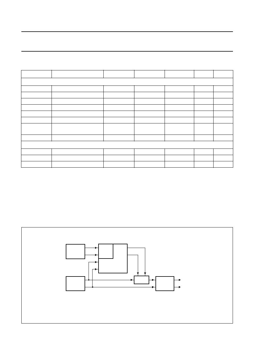
2000 Jan 13
35
Philips Semiconductors
Preliminary specification
Multistandard Picture-In-Picture (PIP)
controller
SAB9079HS
DIGITAL CHARACTERISTICS
All V
DDD(C)
pins = 3.0 to 3.6 V; T
amb
= 0 to 70
∞
C; unless otherwise specified.
Note
1. The internal system frequencies are 3584, 1792, 896 and 448 times the HSYNC input frequency.
TEST AND APPLICATION INFORMATION
TV application with insertion before 100 Hz feature box (double window)
In the 100 Hz application the deflection circuit operates at 100 Hz. The PIP data is inserted into the main decoder output
stream and fed to the feature box. The double window feature is made at 1Fh and the field rate is doubled in the feature
box. The internal synchronization is illustrated in Fig.9.
SYMBOL
PARAMETER
CONDITIONS
MIN.
TYPE
MAX.
UNIT
DC characteristics
V
IH
HIGH-level input voltage
70
-
-
%V
DDD
V
IL
LOW-level input voltage
-
-
30
%V
DDD
V
hys
hysteresis voltage
-
30
-
%V
DDD
V
OH
HIGH-level output voltage
V
DDD(P)
-
0.4
-
-
V
V
OL
LOW-level output voltage
-
-
0.4
V
I
LI
input leakage current
V
DDD
= 3.6 V
-
0.1
1
µ
A
I
OZ
3-state input leakage
current
V
DDD
= 3.6 V
-
0.2
1
µ
A
R
pu
internal pull-up resistor
23
50
80
k
AC characteristics
f
sys
system frequency
note 1
-
3584xHSYNC
kHz
t
r
rise time
-
6
25
ns
t
f
fall time
-
6
25
ns
handbook, full pagewidth
MGS829
Y*UV
MAIN AND
DISPLAY
SUB
DECODER
HV
DECODER
SWITCH
Y*UV
FEATURE
BOX
HV
Y*UV
HV
HV
Y*UV/RGB
FBL
Fig.9 1Fh/1Fv application with insertion before the feature box.
2000 Jan 13
36
Philips Semiconductors
Preliminary specification
Multistandard Picture-In-Picture (PIP)
controller
SAB9079HS
S
LAVE
2F
H GENERAL DESCRIPTION
In the slave mode the main and display channel has to
follow an external 2Fh, xFv signal. The main acquisition
cannot handle such a source, the main/display PLL can.
Thus no main channel PIP is available, only the
upconverted sub channel can be inserted. The following
functions are available in 4 : 1 : 1 only unless otherwise
indicated:
∑
Suitable for single PIP, multi PIP, replay and channel
overview applications
∑
Data formats 4 : 1 : 1 (all modes) and 4 : 2 : 2 (some
modes)
∑
PIP OSD for the sub channels displayed
∑
Detection of PAL/NTSC with overrule bit
∑
CTE and LTE like circuits in display part
∑
Replay with definable auto increment, picture sample
rate and picture number auto wrap
∑
Programmable Y*UV to RGB conversion matrix with
independent coefficients for NTSC and PAL sources
∑
Display clock and synchronization are derived from the
main channel PLL.
The following features are only available for the sub
channel:
∑
Sample rate of 14 Mhz, 720 Y* pixels/line
∑
Horizontal reduction factors
1
/
1
1
/
2
,
1
/
3
,
1
/
4
and
1
/
6
∑
Vertical reduction factors
1
/
1
,
1
/
2
,
1
/
3
and
1
/
4
.
2F
H
, 1F
V ALGORITHMS
Table 26 Available 2Fh and 1Fv algorithms
Notes
1. Median filtering in 4 : 2 : 2 mode is allowed for single PIP (no main channel) and reduction factors not greater than
1
/
2
for both horizontal and vertical
2. The performance of the line doubling algorithm is dependent on the picture content. Line (based interlace) flickering
will remain in this mode.
2F
H
, 2F
V ALGORITHMS
Table 27 Available 2Fh and 2Fv algorithms
Note
1. Median filtering in 4 : 2 : 2 mode is allowed for single PIP (no main channel) and reduction factors not greater than
1
/
2
for both horizontal and vertical
ALGORITHM
FORMAT 4 : 1 : 1
FORMAT 4 : 2 : 2
REMARKS
progressive scan
yes
no; note 1
proscan (median filtering)
line doubling
yes
yes
note 2
ALGORITHM
FORMAT 4 : 1 : 1
FORMAT 4 : 2 : 2
REMARKS
AABB field doubling
yes
yes
ABAB field doubling
yes
yes
AB'A'B fields interpolation
via median filtering
yes
no; note 1
digital scan
AB'A'B+ field interpolation
via median filtering and
averaging with original
fields
yes
no; note 1
digital scan plus

2000 Jan 13
37
Philips Semiconductors
Preliminary specification
Multistandard Picture-In-Picture (PIP)
controller
SAB9079HS
S
LAVE
2F
H AND X
F
V RELATED
I
2
C-
BUS REGISTERS
Table 28 Overview of the I
2
C-bus registers and their subaddresses
D2FH and D2FV
These bits control the display mode with respect to 2Fh or 100 Hz features. If D2FH is set to logic 1 the number of lines
is doubled and/or if D2FV is set to logic 1 the number of fields is doubled.
ABMode
These bits select the different algorithms for 2Fh modes; see Table 29.
Algorithm selection
Several display algorithms can be set with these bits; an overview is given in Table 29.
Note: BGVfp
The resolution of the MAVfp bits changes in 2Fh and xFv modes. In 2Fh and 1Fv modes the vertical resolution is
2 lines/field/step on 1Fh base. In 2Fh and 2Fv modes the vertical resolution is 2 lines/field/step on 2Fh base.
Table 29 Overview of algorithm selection
SUB
ADDRESS
DATA BYTES
BIT 7
BIT 6
BIT 5
BIT 4
BIT 3
BIT 2
BIT 1
BIT 0
01H
D2FH
D2FV
-
-
MFld
(1:0)
SFld
(1:0)
02H
YUVFilter
(1:0)
ABMode
(1:0)
CTE
LTE
(2:0)
MODE
D2FH
YUVFilter
D2FV
ABMode
No filter
0
00H
-
00H
UV 1 : 1 V filter
0
01H
0
00H
Y 1 : 1 V filter
0
10H
0
00H
YUV 1 : 1 V filter
0
11H
0
00H
2FH/1FV frame
1
xxH
0
00H
2FH/1FV proscan
1
xxH
0
01H
2FH/1FV line doubling
1
xxH
0
10H
not valid
1
xxH
0
11H
2FH/2FV AABB
1
00H
1
00H
2FH/2FV ABAB
1
00H
1
01H
2FH/2FV AB'A'B
1
00H
1
10H
2FH/2FV AB'A'B+
1
00H
1
11H
2000 Jan 13
38
Philips Semiconductors
Preliminary specification
Multistandard Picture-In-Picture (PIP)
controller
SAB9079HS
S
LAVE
2F
H MEMORY REQUIREMENTS
In the slave 2Fh modes only the sub picture can be present. The following conditions must be met:
∑
When vertical reduction is 1, the field mode can be set to 3
∑
When vertical reduction is not equal to 1, the field mode must be set to 4
∑
When no live picture is present, such as replay or channel overview, the field mode can be set to 1.
Under these conditions a maximum number of stored fields/pictures can be determined. Combined with the size of one
picture, the total amount needed can be calculated always supposing that 1 PIP is live.
A selected overview is given in Table 30. The VDRAM size is 262144 words of 16 bits
Table 30 Memory requirements for 2Fh slave
S
LAVE
2F
H DESIGN RESTRICTIONS
The design has margins for a 2Fh frequency of 31.5 kHz. Applying a SVGA source with a horizontal frequency of 38 kHz
will stress the SAB9079HS. Therefore, a SVGA source can only be applied under the following restricted conditions:
∑
Power supply spread of 5% instead of 10%
∑
No VCR like phase jump in 2Fh signal.
Table 31 Design characteristics
Note
1. The PLL will lock within 20 lines to instable sources with a large phase jump if the frequency is within the range
28 to 36 kHz.
2. The PLL will lock to stable 2Fh sources with a maximum frequency of 60 kHz.
MODE
PICTURES
STORED
PICTURE SIZE
NTSC (WORDS)
TOTAL NTSC
PICTURE SIZE
PAL (WORDS)
TOTAL PAL
2
◊
V1_H2
4
46284
185136
56028
224112
4
◊
V2_H2
7
23142
161994
28014
196098
6
◊
V2_H3
9
15390
138510
18630
167670
9
◊
V3_H3
12
10260
123120
12420
149040
12
◊
V4_H3
15
7695
115425
9315
139725
16
◊
V4_H4
19
5928
112632
7176
136344
SYMBOL
PARAMETER
CONDITIONS
MIN.
TYP.
MAX.
UNIT
Supplies
V
DDD(P)
all digital supply voltages
for periphery
4.75
5.0
5.25
V
V
DDD(C)
all digital supply voltages
for core
3.15
3.3
3.6
V
V
DDA
all analog supply voltages
3.15
3.3
3.6
V
V
SS
all ground voltages
-
0
-
V
Main PLL and clock generation
f
i(PLL)
note 1
28
31.50
36
kHz
note 2
-
-
60
kHz
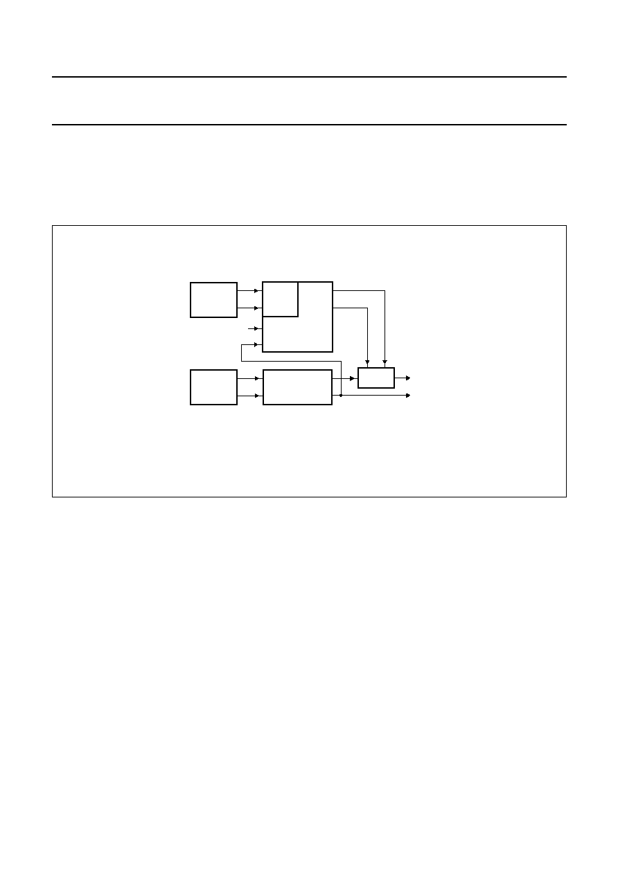
2000 Jan 13
39
Philips Semiconductors
Preliminary specification
Multistandard Picture-In-Picture (PIP)
controller
SAB9079HS
TV
APPLICATION WITH INSERTION AFTER
100 H
Z
(
SLAVE
)
In this application there is no relationship between the deflection and acquisition circuits. A double window feature can
be realized by letting the feature box compress one window and make the second window by the SAB9079HS. In this
application the HVSYNC of the feature box/line doubler is connected to the main acquisition HVSYNC. The restriction is
that no main PIPs can be displayed. The application diagram is illustrated in Fig.10.
handbook, full pagewidth
MGS830
Y*UV
DISPLAY
SUB
DECODER
HV
HV
DECODER
SWITCH
Y*UV
FEATURE BOX/
LINE DOUBLER
HV
Y*UV (not used)
HV
Y*UV/RGB
FBL
Fig.10 2Fh/1Fh application with insertion after the feature box/line doubler.
Instead of the feature box a SVGA signal can be applied.

2000 Jan 13
40
Philips Semiconductors
Preliminary specification
Multistandard Picture-In-Picture (PIP)
controller
SAB9079HS
Master 2Fh general description
A 1Fh, 1Fv signal at the acquisition side can be
upconverted to a 2Fh, 1Fv or a 2Fh, 2Fv signal. The
restriction is that both acquisition channels will be
upconverted at the same time.Therefore, the main channel
displayed as 1Fh, 1Fv combined with a sub channel
displayed as 2Fh, 1Fv is not possible. In the master mode
the SAB9079HS generates the HSYNC and VSYNC for
display/deflection. There is no protection built in. HSYNC
and VSYNC cannot be coupled directly to a tube. A
deflection IC should be applied. Both main and sub
pictures can be acquired/displayed. The following
functions are available:
∑
Suitable for single PIP, some multi PIP modes, replay
and channel overview applications
∑
Data formats 4 : 1 : 1 (all modes) and 4 : 2 : 2 (some
modes)
∑
Sample rate of 14 Mhz, 720 Y* pixels/line
∑
Horizontal reduction factors for main channel
1
/
1
3
/
4
,
2
/
3
,
1
/
2
,
1
/
3
,
1
/
4
and
1
/
6
∑
Horizontal reduction factors for sub channel
1
/
1
3
/
4
,
2
/
3
,
1
/
2
,
1
/
3
,
1
/
4
and
1
/
6
∑
Vertical reduction factors
1
/
1
,
1
/
2
,
1
/
3
and
1
/
4
.
∑
PIP OSD for the sub channels displayed
∑
Detection of PAL/NTSC with overrule bit
∑
CTE and LTE like circuits in display mode
∑
Replay with definable auto increment, picture sample
rate and picture number auto wrap
∑
Programmable Y*UV to RGB conversion matrix with
independent coefficients for NTSC and PAL sources
∑
Display clock and synchronization are derived from the
main channel PLL.
2F
H
, 1F
V ALGORITHMS
Table 32 Available 2Fh and 1Fv algorithms
Notes
1. Median filtering in 4 : 2 : 2 mode is allowed for single PIP (no main channel) and reduction factors not greater than
1
/
2
for both horizontal and vertical
2. The performance of the line doubling algorithm is dependent on the picture content. Line (based interlace) flickering
will remain in this mode.
2F
H
, 2F
V ALGORITHMS
Table 33 Available 2Fh and 2Fv algorithms
Note
1. Median filtering in 4 : 2 : 2 mode is allowed for single PIP (no main channel) and reduction factors not greater than
1
/
2
for both horizontal and vertical
ALGORITHM
FORMAT 4 : 1 : 1
FORMAT 4 : 2 : 2
REMARKS
progressive scan
yes
no; note 1
proscan (median filtering)
line doubling
yes
yes
note 2
ALGORITHM
FORMAT 4 : 1 : 1
FORMAT 4 : 2 : 2
REMARKS
AABB field doubling
yes
yes
ABAB field doubling
yes
yes
AB'A'B fields interpolation
via median filtering
yes
no; note 1
digital scan
AB'A'B+ field interpolation
via median filtering and
averaging with original
fields
yes
no; note 1
digital scan plus

2000 Jan 13
41
Philips Semiconductors
Preliminary specification
Multistandard Picture-In-Picture (PIP)
controller
SAB9079HS
M
ASTER
2F
H AND X
F
V RELATED
I
2
C-
BUS REGISTERS
Table 34 Overview of the I
2
C-bus registers and their subaddresses
SUB
ADDRESS
DATA BYTES
BIT 7
BIT 6
BIT 5
BIT 4
BIT 3
BIT 2
BIT 1
BIT 0
01H
D2FH
D2FV
DMaster
DVSPos
MFld
(1:0)
SFld
(1:0)
02H
YUVFilter
(1:0)
ABMode
(1:0)
CTE
LTE
(2:0)
26H
-
-
-
HSWidth
27H
-
-
VSDel
28H
-
-
-
VSWidth
D2FH, D2FV, DMaster and DVSPos
These bits control the display mode with respect to 2Fh or
100 Hz features. If D2FH is set to logic 1 the number of
lines is doubled and/or if D2FV is set to logic 1 the number
of fields is doubled.
If DMaster is at logic 0 the device is in slave mode.
DHSYNC and DVSYNC should not be used. If DMaster is
at logic 1 the device is in master mode which means that
HV synchronization signals are generated. They are
derived from MHSYNC and MVSYNC. The DHSYNC and
DVSYNC output signals should be used as sync signals
for the deflection IC.
DVSPos is only valid if DMaster is set to logic 1. If DVSPos
is set to logic 0 the VSYNC pulses are generated with an
alternating field ID according to the ABAB algorithm. If
DVSPos is set to logic 1 the VSYNC pulses are generated
in the AABB scheme which means that two first fields are
alternated with two second fields.
ABMode
These bits select the different algorithms for 2Fh modes;
see Table 35.
HSWidth
The width of the DHSYNC can be set in the master mode.
The width is from 0 to 31 pixels and the resolution is one
2Fh pixel.
VSWidth
The width of the DVSYNC can be set in the master mode.
The scale is from 0 to 31 lines on a 2Fh base and the
resolution is
1
/
2
2Fh.
VSDel
The position of the DVSYNC, with respect to the incoming
MVSYNC, can be set in the master mode. The delay is a
6-bit value and the steps are from 0 to 63 lines on a 2Fh
base and the resolution is
1
/
2
2Fh line.
Algorithm selection
Several display algorithms can be set with these bits; an
overview is given in Table 35.
Note: BGVfp
The resolution of the BGVfp bits changes in 2Fh and xFv
modes. In 2Fh and 1Fv modes the vertical resolution is
2 lines/field/step on 1Fh base. In 2Fh and 2Fv modes the
vertical resolution is 2 lines/field/step on 2Fh base.

2000 Jan 13
42
Philips Semiconductors
Preliminary specification
Multistandard Picture-In-Picture (PIP)
controller
SAB9079HS
Table 35 Overview of algorithm selection
F
IELD MODE SETTINGS
In the master mode signals will be synchronized to the main 1Fh, 1Fv input signal. This eases the restrictions on the
number of fields to be stored for the scan converted main picture. Conditions to be met for a live picture are given in
Table 36.
Table 36 Master 2Fh field mode settings
MODE
D2FH
YUVFilter
D2FV
ABMode
No filter
0
00H
-
00H
UV 1 : 1 V filter
0
01H
0
00H
Y 1 : 1 V filter
0
10H
0
00H
YUV 1 : 1 V filter
0
11H
0
00H
2FH/1FV frame
1
xxH
0
00H
2FH/1FV proscan
1
xxH
0
01H
2FH/1FV line doubling
1
xxH
0
10H
not valid
1
xxH
0
11H
2FH/2FV AABB
1
00H
1
00H
2FH/2FV ABAB
1
00H
1
01H
2FH/2FV AB'A'B
1
00H
1
10H
2FH/2FV AB'A'B+
1
00H
1
11H
VERTICAL REDUCTION
FIELDS FOR MAIN
CHANNEL
FIELDS FOR SUB
CHANNEL
REMARKS
1/1
2
3
except for horizontal
reduction 1/1
other modes
4
4
-

2000 Jan 13
43
Philips Semiconductors
Preliminary specification
Multistandard Picture-In-Picture (PIP)
controller
SAB9079HS
F
EATURE BOX APPLICATION
100 H
Z
(
MASTER
)
In this mode the SAB9079HS generates the display clock which is derived from the main clock and synchronization
signals. The whole system runs at one PLL. Only full screen images of the main decoder are handled. The PIP insertion
of the sub channel is not required here; see Fig.11.
D
OUBLE WINDOW AND
/
OR OTHER
PIP
FUNCTIONS AT
100 H
Z
(
MASTER
)
This is the same configuration as Fig.11 but the sub channel is also needed and, therefore, a second PLL. The
constraints apply with respect to the memory use and performance. Double window PAL is only possible if bit SmlPal is
set to logic 1, this is due to the memory limitations.
D
OUBLE WINDOW AND
/
OR OTHER
PIP
FUNCTIONS AT
2F
H
, 1F
V
(
MASTER
)
For the application diagram please refer to Fig.12.
handbook, full pagewidth
MGS831
Y*UV (not used)
DISPLAY
SUB
HV (not used)
Y*UV
DECODER
DEFLECTION
HV
Y*UV
HV
Y*UV/RGB
HV
Fig.11 100 Hz application with ECO-100 Hz function.
handbook, full pagewidth
MGS832
Y*UV
DISPLAY
SUB
DECODER
HV
Y*UV
DECODER
DEFLECTION
HV
Y*UV
HV
Y*UV/RGB
HV
Fig.12 100 Hz application with 2 channel PIP function.
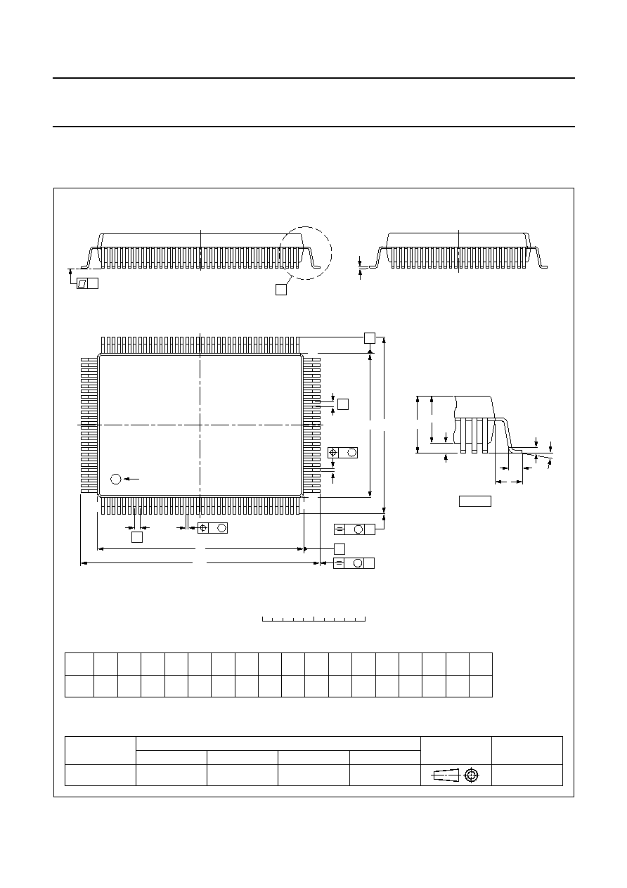
2000 Jan 13
44
Philips Semiconductors
Preliminary specification
Multistandard Picture-In-Picture (PIP)
controller
SAB9079HS
PACKAGE OUTLINE
UNIT
A1
min.
A
2
A
3
b
p
c
E
(1)
e
H
E
L
L
p
y
w
v
REFERENCES
OUTLINE
VERSION
EUROPEAN
PROJECTION
ISSUE DATE
IEC
JEDEC
EIAJ
mm
2.90
2.50
0.25
0.25
0.27
0.17
0.23
0.11
14.1
13.9
0.50
17.35
17.05
7
∞
0
∞
0.08
0.20
1.60
0.08
DIMENSIONS (mm are the original dimensions)
Note
1. Plastic or metal protrusions of 0.25 mm maximum per side are not included.
1.03
0.73
SOT387-3
98-03-27
D
(1)
20.1
19.9
H
D
23.35
23.05
pin 1 index
b
p
e
E
A
1
A
L
p
detail X
L
(A )
3
B
38
c
D
H
b
p
E
H
A
2
v
M
B
D
A
e
v
M
A
1
128
103
102
65
64
39
w
M
w
M
0
5
10 mm
scale
SQFP128: plastic shrink quad flat package;
128 leads (lead length 1.6 mm); body 14 x 20 x 2.72 mm
SOT387-3
A
max.
3.40
X
y

2000 Jan 13
45
Philips Semiconductors
Preliminary specification
Multistandard Picture-In-Picture (PIP)
controller
SAB9079HS
SOLDERING
Introduction to soldering surface mount packages
This text gives a very brief insight to a complex technology.
A more in-depth account of soldering ICs can be found in
our
"Data Handbook IC26; Integrated Circuit Packages"
(document order number 9398 652 90011).
There is no soldering method that is ideal for all surface
mount IC packages. Wave soldering is not always suitable
for surface mount ICs, or for printed-circuit boards with
high population densities. In these situations reflow
soldering is often used.
Reflow soldering
Reflow soldering requires solder paste (a suspension of
fine solder particles, flux and binding agent) to be applied
to the printed-circuit board by screen printing, stencilling or
pressure-syringe dispensing before package placement.
Several methods exist for reflowing; for example,
infrared/convection heating in a conveyor type oven.
Throughput times (preheating, soldering and cooling) vary
between 100 and 200 seconds depending on heating
method.
Typical reflow peak temperatures range from
215 to 250
∞
C. The top-surface temperature of the
packages should preferable be kept below 230
∞
C.
Wave soldering
Conventional single wave soldering is not recommended
for surface mount devices (SMDs) or printed-circuit boards
with a high component density, as solder bridging and
non-wetting can present major problems.
To overcome these problems the double-wave soldering
method was specifically developed.
If wave soldering is used the following conditions must be
observed for optimal results:
∑
Use a double-wave soldering method comprising a
turbulent wave with high upward pressure followed by a
smooth laminar wave.
∑
For packages with leads on two sides and a pitch (e):
≠ larger than or equal to 1.27 mm, the footprint
longitudinal axis is preferred to be parallel to the
transport direction of the printed-circuit board;
≠ smaller than 1.27 mm, the footprint longitudinal axis
must be parallel to the transport direction of the
printed-circuit board.
The footprint must incorporate solder thieves at the
downstream end.
∑
For packages with leads on four sides, the footprint must
be placed at a 45
∞
angle to the transport direction of the
printed-circuit board. The footprint must incorporate
solder thieves downstream and at the side corners.
During placement and before soldering, the package must
be fixed with a droplet of adhesive. The adhesive can be
applied by screen printing, pin transfer or syringe
dispensing. The package can be soldered after the
adhesive is cured.
Typical dwell time is 4 seconds at 250
∞
C.
A mildly-activated flux will eliminate the need for removal
of corrosive residues in most applications.
Manual soldering
Fix the component by first soldering two
diagonally-opposite end leads. Use a low voltage (24 V or
less) soldering iron applied to the flat part of the lead.
Contact time must be limited to 10 seconds at up to
300
∞
C.
When using a dedicated tool, all other leads can be
soldered in one operation within 2 to 5 seconds between
270 and 320
∞
C.

2000 Jan 13
46
Philips Semiconductors
Preliminary specification
Multistandard Picture-In-Picture (PIP)
controller
SAB9079HS
Suitability of surface mount IC packages for wave and reflow soldering methods
Notes
1. All surface mount (SMD) packages are moisture sensitive. Depending upon the moisture content, the maximum
temperature (with respect to time) and body size of the package, there is a risk that internal or external package
cracks may occur due to vaporization of the moisture in them (the so called popcorn effect). For details, refer to the
Drypack information in the
"Data Handbook IC26; Integrated Circuit Packages; Section: Packing Methods".
2. These packages are not suitable for wave soldering as a solder joint between the printed-circuit board and heatsink
(at bottom version) can not be achieved, and as solder may stick to the heatsink (on top version).
3. If wave soldering is considered, then the package must be placed at a 45
∞
angle to the solder wave direction.
The package footprint must incorporate solder thieves downstream and at the side corners.
4. Wave soldering is only suitable for LQFP, TQFP and QFP packages with a pitch (e) equal to or larger than 0.8 mm;
it is definitely not suitable for packages with a pitch (e) equal to or smaller than 0.65 mm.
5. Wave soldering is only suitable for SSOP and TSSOP packages with a pitch (e) equal to or larger than 0.65 mm; it is
definitely not suitable for packages with a pitch (e) equal to or smaller than 0.5 mm.
PACKAGE
SOLDERING METHOD
WAVE
REFLOW
(1)
BGA, SQFP
not suitable
suitable
HLQFP, HSQFP, HSOP, HTSSOP, SMS
not suitable
(2)
suitable
PLCC
(3)
, SO, SOJ
suitable
suitable
LQFP, QFP, TQFP
not recommended
(3)(4)
suitable
SSOP, TSSOP, VSO
not recommended
(5)
suitable

2000 Jan 13
47
Philips Semiconductors
Preliminary specification
Multistandard Picture-In-Picture (PIP)
controller
SAB9079HS
DEFINITIONS
LIFE SUPPORT APPLICATIONS
These products are not designed for use in life support appliances, devices, or systems where malfunction of these
products can reasonably be expected to result in personal injury. Philips customers using or selling these products for
use in such applications do so at their own risk and agree to fully indemnify Philips for any damages resulting from such
improper use or sale.
PURCHASE OF PHILIPS I
2
C COMPONENTS
Data sheet status
Objective specification
This data sheet contains target or goal specifications for product development.
Preliminary specification
This data sheet contains preliminary data; supplementary data may be published later.
Product specification
This data sheet contains final product specifications.
Limiting values
Limiting values given are in accordance with the Absolute Maximum Rating System (IEC 134). Stress above one or
more of the limiting values may cause permanent damage to the device. These are stress ratings only and operation
of the device at these or at any other conditions above those given in the Characteristics sections of the specification
is not implied. Exposure to limiting values for extended periods may affect device reliability.
Application information
Where application information is given, it is advisory and does not form part of the specification.
Purchase of Philips I
2
C components conveys a license under the Philips' I
2
C patent to use the
components in the I
2
C system provided the system conforms to the I
2
C specification defined by
Philips. This specification can be ordered using the code 9398 393 40011.

© Philips Electronics N.V.
SCA
All rights are reserved. Reproduction in whole or in part is prohibited without the prior written consent of the copyright owner.
The information presented in this document does not form part of any quotation or contract, is believed to be accurate and reliable and may be changed
without notice. No liability will be accepted by the publisher for any consequence of its use. Publication thereof does not convey nor imply any license
under patent- or other industrial or intellectual property rights.
Internet: http://www.semiconductors.philips.com
2000
69
Philips Semiconductors ≠ a worldwide company
For all other countries apply to: Philips Semiconductors,
International Marketing & Sales Communications, Building BE-p, P.O. Box 218,
5600 MD EINDHOVEN, The Netherlands, Fax. +31 40 27 24825
Argentina: see South America
Australia: 3 Figtree Drive, HOMEBUSH, NSW 2140,
Tel. +61 2 9704 8141, Fax. +61 2 9704 8139
Austria: Computerstr. 6, A-1101 WIEN, P.O. Box 213,
Tel. +43 1 60 101 1248, Fax. +43 1 60 101 1210
Belarus: Hotel Minsk Business Center, Bld. 3, r. 1211, Volodarski Str. 6,
220050 MINSK, Tel. +375 172 20 0733, Fax. +375 172 20 0773
Belgium: see The Netherlands
Brazil: see South America
Bulgaria: Philips Bulgaria Ltd., Energoproject, 15th floor,
51 James Bourchier Blvd., 1407 SOFIA,
Tel. +359 2 68 9211, Fax. +359 2 68 9102
Canada: PHILIPS SEMICONDUCTORS/COMPONENTS,
Tel. +1 800 234 7381, Fax. +1 800 943 0087
China/Hong Kong: 501 Hong Kong Industrial Technology Centre,
72 Tat Chee Avenue, Kowloon Tong, HONG KONG,
Tel. +852 2319 7888, Fax. +852 2319 7700
Colombia: see South America
Czech Republic: see Austria
Denmark: Sydhavnsgade 23, 1780 COPENHAGEN V,
Tel. +45 33 29 3333, Fax. +45 33 29 3905
Finland: Sinikalliontie 3, FIN-02630 ESPOO,
Tel. +358 9 615 800, Fax. +358 9 6158 0920
France: 51 Rue Carnot, BP317, 92156 SURESNES Cedex,
Tel. +33 1 4099 6161, Fax. +33 1 4099 6427
Germany: Hammerbrookstraþe 69, D-20097 HAMBURG,
Tel. +49 40 2353 60, Fax. +49 40 2353 6300
Hungary: see Austria
India: Philips INDIA Ltd, Band Box Building, 2nd floor,
254-D, Dr. Annie Besant Road, Worli, MUMBAI 400 025,
Tel. +91 22 493 8541, Fax. +91 22 493 0966
Indonesia: PT Philips Development Corporation, Semiconductors Division,
Gedung Philips, Jl. Buncit Raya Kav.99-100, JAKARTA 12510,
Tel. +62 21 794 0040 ext. 2501, Fax. +62 21 794 0080
Ireland: Newstead, Clonskeagh, DUBLIN 14,
Tel. +353 1 7640 000, Fax. +353 1 7640 200
Israel: RAPAC Electronics, 7 Kehilat Saloniki St, PO Box 18053,
TEL AVIV 61180, Tel. +972 3 645 0444, Fax. +972 3 649 1007
Italy: PHILIPS SEMICONDUCTORS, Via Casati, 23 - 20052 MONZA (MI),
Tel. +39 039 203 6838, Fax +39 039 203 6800
Japan: Philips Bldg 13-37, Kohnan 2-chome, Minato-ku,
TOKYO 108-8507, Tel. +81 3 3740 5130, Fax. +81 3 3740 5057
Korea: Philips House, 260-199 Itaewon-dong, Yongsan-ku, SEOUL,
Tel. +82 2 709 1412, Fax. +82 2 709 1415
Malaysia: No. 76 Jalan Universiti, 46200 PETALING JAYA, SELANGOR,
Tel. +60 3 750 5214, Fax. +60 3 757 4880
Mexico: 5900 Gateway East, Suite 200, EL PASO, TEXAS 79905,
Tel. +9-5 800 234 7381, Fax +9-5 800 943 0087
Middle East: see Italy
Netherlands: Postbus 90050, 5600 PB EINDHOVEN, Bldg. VB,
Tel. +31 40 27 82785, Fax. +31 40 27 88399
New Zealand: 2 Wagener Place, C.P.O. Box 1041, AUCKLAND,
Tel. +64 9 849 4160, Fax. +64 9 849 7811
Norway: Box 1, Manglerud 0612, OSLO,
Tel. +47 22 74 8000, Fax. +47 22 74 8341
Pakistan: see Singapore
Philippines: Philips Semiconductors Philippines Inc.,
106 Valero St. Salcedo Village, P.O. Box 2108 MCC, MAKATI,
Metro MANILA, Tel. +63 2 816 6380, Fax. +63 2 817 3474
Poland: Al.Jerozolimskie 195 B, 02-222 WARSAW,
Tel. +48 22 5710 000, Fax. +48 22 5710 001
Portugal: see Spain
Romania: see Italy
Russia: Philips Russia, Ul. Usatcheva 35A, 119048 MOSCOW,
Tel. +7 095 755 6918, Fax. +7 095 755 6919
Singapore: Lorong 1, Toa Payoh, SINGAPORE 319762,
Tel. +65 350 2538, Fax. +65 251 6500
Slovakia: see Austria
Slovenia: see Italy
South Africa: S.A. PHILIPS Pty Ltd., 195-215 Main Road Martindale,
2092 JOHANNESBURG, P.O. Box 58088 Newville 2114,
Tel. +27 11 471 5401, Fax. +27 11 471 5398
South America: Al. Vicente Pinzon, 173, 6th floor,
04547-130 S√O PAULO, SP, Brazil,
Tel. +55 11 821 2333, Fax. +55 11 821 2382
Spain: Balmes 22, 08007 BARCELONA,
Tel. +34 93 301 6312, Fax. +34 93 301 4107
Sweden: Kottbygatan 7, Akalla, S-16485 STOCKHOLM,
Tel. +46 8 5985 2000, Fax. +46 8 5985 2745
Switzerland: Allmendstrasse 140, CH-8027 ZÐRICH,
Tel. +41 1 488 2741 Fax. +41 1 488 3263
Taiwan: Philips Semiconductors, 6F, No. 96, Chien Kuo N. Rd., Sec. 1,
TAIPEI, Taiwan Tel. +886 2 2134 2886, Fax. +886 2 2134 2874
Thailand: PHILIPS ELECTRONICS (THAILAND) Ltd.,
209/2 Sanpavuth-Bangna Road Prakanong, BANGKOK 10260,
Tel. +66 2 745 4090, Fax. +66 2 398 0793
Turkey: Yukari Dudullu, Org. San. Blg., 2.Cad. Nr. 28 81260 Umraniye,
ISTANBUL, Tel. +90 216 522 1500, Fax. +90 216 522 1813
Ukraine: PHILIPS UKRAINE, 4 Patrice Lumumba str., Building B, Floor 7,
252042 KIEV, Tel. +380 44 264 2776, Fax. +380 44 268 0461
United Kingdom: Philips Semiconductors Ltd., 276 Bath Road, Hayes,
MIDDLESEX UB3 5BX, Tel. +44 208 730 5000, Fax. +44 208 754 8421
United States: 811 East Arques Avenue, SUNNYVALE, CA 94088-3409,
Tel. +1 800 234 7381, Fax. +1 800 943 0087
Uruguay: see South America
Vietnam: see Singapore
Yugoslavia: PHILIPS, Trg N. Pasica 5/v, 11000 BEOGRAD,
Tel. +381 11 3341 299, Fax.+381 11 3342 553
Printed in The Netherlands
545004/50/01/pp
48
Date of release:
2000 Jan 13
Document order number:
9397 750 05258