Document Outline
- DESCRIPTION
- FEATURES
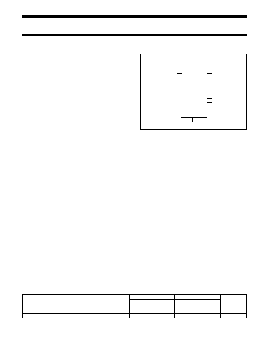
- PIN CONFIGURATIONS
- ORDERING INFORMATION
- PIN CONFIGURATIONS
- ABSOLUTE MAXIMUM RATINGS
- BLOCK DIAGRAM
- PIN DESCRIPTION
- FUNCTIONAL BLOCKS
- BLOCK DIAGRAM
- Channel Blocks
- Data Bus Buffer
- Operation Control
- Timing Circuits
- Time Out Mode Caution
- Receiver and Transmitter
- RECEIVER FIFO
- WAKE-UP MODE (MULTI-DROP OR 9-BIT)
- INPUT OUTPUT (I/O) PINS
- Interrupt Priority System
- Functional Description of the Interrupt Arbitration
- Priority Arbitration and Bidding
- Clearing the Interrupt
- Arbitration - Aftermath
- Interrupt Context
- Interrupt Threshold Calculation
- Vectored Interrupts
- PROGRAMMING UART CONTROL REGISTERS
- Mode Registers 0, 1 and 2
- MR0 Ö Mode Register 0
- MR1 Ö Mode Register 1
- MR2 Ö Mode Register 2
- CR Ö Command Register
- CSR Ö Clock Select Register
- SR Ö Channel Status Register
- ACR Ö Auxiliary Control Register
- IPCR Ö Input Port Change Register
- ISR Ö Interrupt Status Register
- IMR Ö Interrupt Mask Register
- CTUR and CTLR Ö Counter/Timer Registers
- I/O LOGIC
- Registers of the Interrupt System
- DC ELECTRICAL CHARACTERISTICS
- AC ELECTRICAL CHARACTERISTICS
- INTERRUPT NOTES
- NOTE ON QUART INTERFACE TO ITS CONTROLLING PROCESSOR
- The Asynchronous Interface
- The Synchronous Interface
- Summary
Philips Semiconductors
Product specification
SC68C94
Quad universal asynchronous receiver/transmitter (QUART)
1
1995 May 1
853-1601 15179
DESCRIPTION
The 68C94 quad universal asynchronous receiver/transmitter
(QUART) combines four enhanced Philips Semiconductors
industry-standard UARTs with an innovative interrupt scheme that
can vastly minimize host processor overhead. It is implemented
using Philips Semiconductors' high-speed CMOS process that
combines small die size and cost with low power consumption.
The operating speed of each receiver and transmitter can be
selected independently at one of eighteen fixed baud rates, a 16X
clock derived from a programmable counter/timer, or an external 1X
or 16X clock. The baud rate generator and counter/timer can
operate directly from a crystal or from external clock inputs. The
ability to independently program the operating speed of the receiver
and transmitter make the QUART particularly attractive for
dual-speed channel applications such as clustered terminal
systems.
Each receiver is buffered with eight character FIFOs (first-in-first-out
memories) and one shift register to minimize the potential for
receiver overrun and to reduce interrupt overhead in interrupt driven
systems. In addition, a handshaking capability is provided to disable
a remote UART transmitter when the receiver buffer is full. (RTS
control)
The 68C94 provides a power-down mode in which the oscillator is
stopped and the register contents are stored. This results in reduced
power consumption on the order of several magnitudes. The
QUART is fully TTL compatible and operates from a single +5V
power supply.
FEATURES
∑
New low overhead interrupt control
∑
Four Philips Semiconductors industry-standard UARTs
∑
Eight byte receive FIFO and eight byte transmit FIFO for each
UART
∑
Programmable data format:
≠ 5 to 8 data bits plus parity
≠ Odd, even, no parity or force parity
≠ 1, 1.5 or 2 stop bits programmable in 1/16-bit increments
∑
Baud rate for the receiver and transmitter selectable from:
≠ 23 fixed rates: 50 to 230.4K baud Non-standard rates to 1.0M
baud
≠ User-defined rates from the programmable counter/timer
associated with each of two blocks
≠ External 1x or 16x clock
∑
Parity, framing, and overrun error detection
∑
False start bit detection
∑
Line break detection and generation
PIN CONFIGURATIONS
VCC
A5:0
CEN
RDN
WRN
IACKN
RESET
X1/CLK
X2
RDa-d
VSS
D7-0
DACKN
RQN
I/O0a≠d
I/O1a≠d
I/O2a≠d
I/O3a≠d
TDa-d
SD00178
∑
Programmable channel mode
≠ Normal (full-duplex), automatic echo, local loop back, remote
loopback
∑
Programmable interrupt priorities
∑
Identification of highest priority interrupt
∑
Global interrupt register set provides data from interrupting
channel
∑
Vectored interrupts with programmable vector format
∑
IACKN and DTACKN signals
∑
Built-in baud rate generator with choice of 18 rates
∑
Four I/O pins per UART for modem controls, clocks, etc.
∑
Power down mode
∑
High-speed CMOS technology
∑
52-pin PLCC and 48-pin DIP
∑
Commercial and industrial temperature ranges available
∑
On-chip crystal oscillator
∑
TTL compatible
∑
Single +5V power supply with low power mode
∑
Two multifunction programmable 16-bit counter/timers
∑
1MHz 16x mode operation
∑
30ns data bus release time
∑
"Watch Dog" timer for each receiver
ORDERING INFORMATION
PACKAGES
COMMERCIAL
INDUSTRIAL
DWG #
PACKAGES
V
CC
= +5V +10%,
T
A
= 0
o
C to +70
o
C
V
CC
= +5V +10%,
T
A
= ≠40
o
C to +85
o
C
DWG #
48-Pin Plastic Dual In-Line Package (DIP)
SC68C94C1N
SC68C94A1N
SOT240-1
52-Pin Plastic Leaded Chip Carrier (PLCC)
SC68C94C1A
SC68C94A1A
SOT238-3
Philips Semiconductors
Product specification
SC68C94
Quad universal asynchronous receiver/transmitter (QUART)
1995 May 1
2
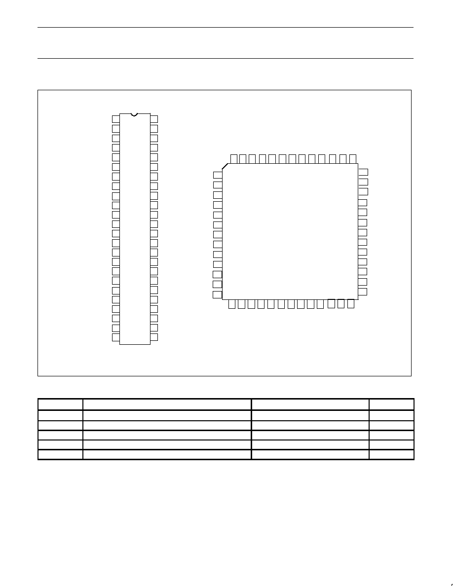
PIN CONFIGURATIONS
46
45
44
48
47
46
45
44
43
42
41
40
39
38
37
36
35
34
33
32
31
30
29
1
2
3
4
5
6
7
8
9
10
11
12
13
14
15
16
17
18
19
20
28
27
26
25
21
22
23
24
X1/CLK
TXDD
RXDD
IRQN
A5
A4
A3
A2
A1
A0
WRN
CEN
RDN
DACKN
IACKN
TXDB
RXDB
D7
D6
D5
D4
D3
D1
D0
RXDA
TXDA
I/O2B
I/O1B
I/O0B
I/O2A
I/O1A
I/O0A
I/O0C
I/O1C
I/O2C
I/O0D
I/O1D
I/O2D
RXDC
TXDC
RESET
X2
VSS
VCC
D2
VSS
VSS
CEN
RDN
DACKN
IACKN
TXDB
RXDB
D7
D6
D5
D4
I/O3B
D1
D0
RXDA
TXDA
I/O2B
I/O1B
I/O0B
I/O3A
I/O2A
D2
VSS
D3
I/O1A
A1
A2
A3
A4
A5
IRQN
RXDD
TXDD
X1/CLK
X2
TXDC
RXDC
I/O2D
I/O1D
I/O0D
I/O3C
I/O2C
I/O1C
I/O0C
RESET
I/O3D
I/O0A
VSS
WRN
A0
48-Pin Dual-In-Line Package
52-Pin PLCC Package
1
2
3
4
5
6
7
8
9
10
11
18
19
20
21
22
23
24
31 32
33
34
35
36
37
50
51
52
38
39
40
41
42
43
25
26
27
28
29
30
12
13
14
15
16
17
47
48
49
V
SS
V
CC
V
SS
VSS
SD00179
ABSOLUTE MAXIMUM RATINGS
1, 2
SYMBOL
PARAMETER
RATING
UNIT
T
A
Operating ambient temperature range
3
Note 4
o
C
T
STG
Storage temperature range
≠65 to +150
o
C
V
CC
Voltage from V
DD
to GND
4
≠0.5 to +7.0
V
V
S
Voltage from any pin to ground
4
≠0.5 to V
CC
+0.5
V
P
D
Power dissipation
1
W
NOTES:
1. Stresses above those listed under Absolute Maximum Ratings may cause permanent damage to the device. This is a stress rating only and
functional operation of the device at these or any other condition above those indicated in the operation section of this specification is not
implied.
2. For operating at elevated temperatures, the device must be derated based on +150
∞
C maximum junction temperature.
3. This product includes circuitry specifically designed for the protection of its internal devices from damaging effects of excessive static
charge. Nonetheless, it is suggested that conventional precautions be taken to avoid applying any voltages larger than the rated maxima.
4. Parameters are valid over specified temperature range. See ordering information table for applicable temperature range and operating
supply range.
Philips Semiconductors
Product specification
SC68C94
Quad universal asynchronous receiver/transmitter (QUART)
1995 May 1
3
BLOCK DIAGRAM
8
D0≠D7
RDN
WRN
CEN
A0≠A5
RESET
X1/CLK
X2
6
BUS BUFFER
OPERATION CONTROL
ADDRESS
DECODE
R/W CONTROL
TIMING
CHANNEL A
MR 0, 1, 2
CR
SR
INPUT PORT
OUTPUT PORT
OPCR
CSR Rx
CSR Tx
CRYSTAL
OSCILLATOR
POWER UP-DOWN
LOGIC
SAME AS
DUART AB
8 BYTE TRANSMIT
FIFO
TRANSMIT SHIFT
REGISTER
8 BYTE
RECEIVE FIFO
RECEIVE SHIFT
REGISTER
CHANGE-OF-
STATE
DETECTORS (4)
IPCR
ACR
FUNCTION SELECT
LOGIC
CHANNEL B
(AS ABOVE)
TIMING
CLOCK
SELECTORS
COUNTER/
TIMER
ACR
CTUR
CTLR
INTERRUPT CONTROL
IMR
ISR
INTERNAL DATA
BUS
TxDA
RxDA
TxDB
RxDB
1:0
4
TIMING
CONTROL
DACKN
DUART CD
TXDC
TXDD
RXDC
RXDD
I/O[3:0]C
I/O[3:0]D
1:0
I/O[3:0]B
I/O[3:0]A
∑
VCC
∑
VSS1
∑
VSS2
∑
VSS3
∑
VSS4
BAUD RATE
GENERATOR
DUART AB
LOGIC
GLOBAL
REGISTERS
IRQN
IACKN
INTERRUPT ARBITRATION
8
DUART
COMMON
AB
18
4
4
4
˜
2
SD00180
Philips Semiconductors
Product specification
SC68C94
Quad universal asynchronous receiver/transmitter (QUART)
1995 May 1
4
PIN DESCRIPTION
MNEMONIC
TYPE
NAME AND FUNCTION
CEN
I
Chip Select: Active low input that, in conjunction with RDN or WRN, indicates that the host MPU is trying to
access a QUART register. CEN must be inactive when IACKN is asserted.
A5:0
I
Address Lines: These inputs select a 68C94 register to be read or written by the host MPU.
D7:0
I/O
8-bit Bidirectional Data Bus: Used by the host MPU to read and write 68C94 registers.
RDN
I
Read Strobe: Active low input. When this line is asserted simultaneously with CEN, the 68C94 places the
contents of the register selected by A5:0 on the D7:0 lines.
WRN
I
Write Strobe: Active low input. When this line is asserted simultaneously with CEN, the 68C94 writes the data
on D7:0 into the register selected by A5:0.
DACKN
O
Data ACKnowledge: Active low, open-drain output to the host MPU, which is asserted subsequent to a read or
write operation. For a read operation, assertion of DACKN indicates that register data is valid on D7:0. For a
write operation, it indicates that the data on D7:0 has been captured into the indicated register. This signal
corresponds to READYN on 80x86 processors and DTACKN on 680x0 processors.
IRQN
O
Interrupt Request: This active low open-drain output to the host MPU indicating that one or more of the
enabled UART interrupt sources has reached an interrupt value which exceeds that pre-programmed by host
software. The IRQN can be used directly as a 680x0 processor input; it must be inverted for use as an 80x86
interrupt input. This signal requires an external pull-up resistor.
IACKN
I
Interrupt ACKnowledge: Active low input indicates host MPU is acknowledging an interrupt requested. The
68C94 responds by placing an interrupt vector or interrupt vector modified on D7-D0 and asserting DACKN. This
signal updates the CIR register in the interrupt logic. CEN must be high during this cycle.
TDa-d
O
Transmit Data: Serial outputs from the four UARTs.
RDa-d
I
Receive Data: Serial inputs to the four UARTs/
I/O0a-d
I/O
Input/Output 0: A multi-use input or output signal for each UART. These pins can be used as general purpose
inputs, Clear to Send inputs, 1X or 16X Transmit Clock outputs or general purpose outputs. Change-of-state
detection is provided for these pins.
I/O1a-d
I/O
Input/Output 1: A multi-use input or output signal for each UART. These pins can be used as general purpose
or 1X or 16X transmit clock inputs, or general purpose 1X or 16X receive clock outputs. Change-of-state
detection is provided for these pins. In addition, I/O1a and I/O1c can be used as Counter/Timer inputs and I/O1b
and I/O1d can be used as Counter/Timer outputs.
I/O2a-d
I/O
Input/Output 2: A multi-use input or output signal for each UART. These pins can be used as general purpose
inputs, 1X or 16X receive clock inputs, general purpose outputs, RTS output or 1X or 16X receive clock outputs.
I/O3a-d
I/O
Input/Output 3: A multi-use input or output signal for each UART. These pins can be used as general purpose
inputs, 1X or 16X transmit clock inputs, general purpose outputs, or 1X or 16X transmit clock outputs.
RESET
I
Master Reset: Active high reset for the 68C94 logic. Must be asserted at power-up, may be asserted at other
times that the system is to be reset and restarted. OSC set to divide by 1, MR pointer set to 1, DACKN enabled,
I/O pins to input. Registers reset: OPR, CIR. IRQN, DTACKN, IVR Interrupt Vector, Power Down, Test registers,
FIFO pointers, Baud rate generator, Error Status, Watch Dog Timers, Change of State detectors, counter/timer to
timer, Transmitter and Receiver controllers and all interrupt bits. If reset pin is not used, then first chip access
should be to celar `power-down' mode.
X1/CLK
I
Crystal 1 or Communication Clock: This pin is normally connected to one side of a 3.6864MHz or a
7.3728MHz crystal, or can be connected to an external clock up to 8MHz.
X2
O
Crystal 2: If a crystal is used, this pin should be connected to its other terminal. If an external clock is applied to
X1, this pin should be left unconnected.
V
CC
, V
SS
Power and grounds: respectively.
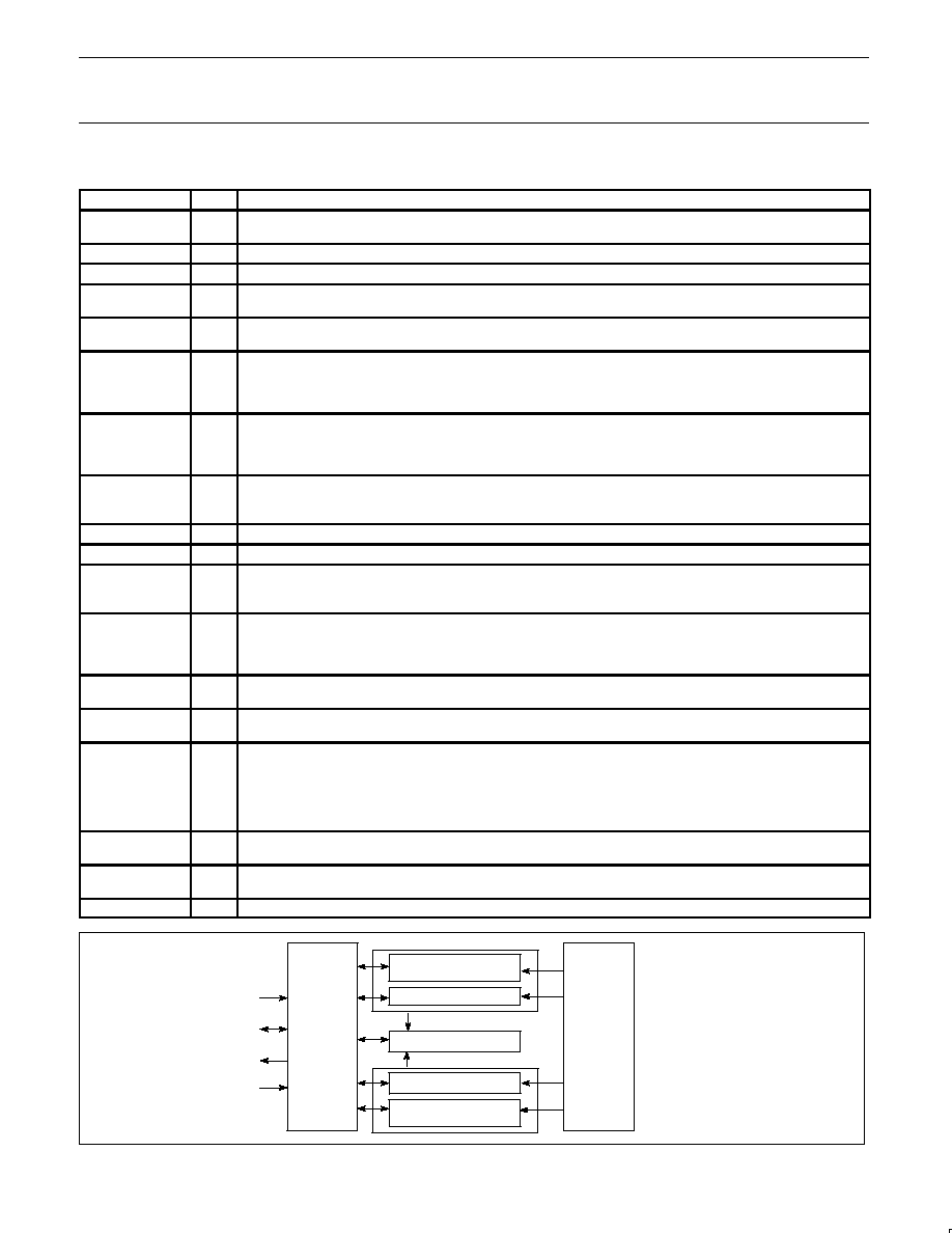
COUNTER/TIMER
I/O PORT CONTROL
UARTS A/B
INTERRUPT CONTROL
BLOCK B
UARTS C/D
I/O CONTROL
I/O PORT CONTROL
A0-A5
D (7:0)
DTACKN
IACKN
BAUD
RATE
GENERATOR
BUS
INTERFACE
BLOCK A
SD00161
Figure 1. Channel Architecture
Philips Semiconductors
Product specification
SC68C94
Quad universal asynchronous receiver/transmitter (QUART)
1995 May 1
5
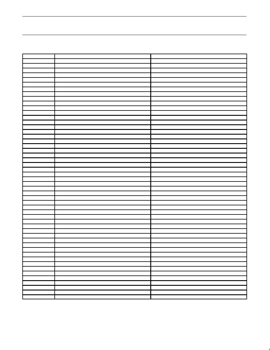
Table 1.
QUART Registers
1
A5:0
READ (RDN = Low)
WRITE (WRN = Low)
000000
Mode Register a (MR0a, MR1a, MR2a)
Mode Register a (MR0a, MR1a, MR2a)
000001
Status Register a (SRa)
Clock Select Register a (CSRa)
000010
Reserved
Command Register a (CRa)
000011
Receive Holding Register a (RxFIFOa)
Transmit Holding Register a (TxFIFOa)
000100
Input Port Change Reg ab (IPCRab)
Auxiliary Control Reg ab (ACRab)
000101
Interrupt Status Reg ab (ISRab)
Interrupt Mask Reg ab (IMRab)
000110
Counter/Timer Upper ab (CTUab)
Counter/Timer Upper Reg ab (CTURab)
000111
Counter/Timer Lower ab (CTLab)
Counter/Timer Lower Reg ab (CTLRab)
001000
Mode Register b (MR0b, MR1b, MR2b)
Mode Register b (MR0b, MR1b, MR2b)
001001
Status Register b (SRb)
Clock Select Register b (CSRb)
001010
Reserved
Command Register b (CRb)
001011
Receive Holding Register b (RxFIFOb)
Transmit Holding Register b (TxFIFOb)
001100
Output Port Register ab (OPRab)
Output Port Register ab (OPRab)
001101
Input Port Register ab (IPRab)
I/OPCRa (I/O Port Control Reg a)
001110
Start Counter ab
I/OPCRb (I/O Port Control Reg b)
001111
Stop Counter ab
Reserved
010000
Mode Register c (MR0c, MR1c, MR2c)
Mode Register c (MR0c, MR1c, MR2c)
010001
Status Register c (SRc)
Clock Select Register c (CSRc)
010010
Reserved
Command Register c (CRc)
010011
Receive Holding Register c (RxFIFOc)
Transmit Holding Register c (TxFIFOc)
010100
Input Port Change Reg cd (IPCRcd)
Auxiliary Control Reg cd (ACRcd)
010101
Interrupt Status Reg cd (ISRcd)
Interrupt Mask Reg cd (IMRcd)
010110
Counter/Timer Upper cd (CTUcd)
Counter/Timer Upper Reg cd (CTURcd)
010111
Counter/Timer Lower cd (CTLcd)
Counter/Timer Lower Reg cd (CTLRcd)
011000
Mode Register d (MR0d, MR1d, MR2d)
Mode Register d (MR0d, MR1d, MR2d)
011001
Status Register d (SRd)
Clock Select Register d (CSRd)
011010
Reserved
Command Register d (CRd)
011011
Receive Holding Register d (RxFIFOd)
Transmit Holding Register d (TxFIFOd)
011100
Output Port Register cd (OPRcd)
Output Port Register cd (OPRcd)
011101
Input Port Register cd (IPRcd)
I/OPCRc (I/O Port Control Reg c)
011110
Start Counter cd
I/OPCRd (I/O Port Control Reg d)
011111
Stop Counter cd
Reserved
100000
Bidding Control Register a (BCRa)
Bidding Control Register a (BCRa)
100001
Bidding Control Register b (BCRb)
Bidding Control Register b (BCRb)
100010
Bidding Control Register c (BCRc)
Bidding Control Register c (BCRc)
100011
Bidding Control Register d (BCRd)
Bidding Control Register d (BCRd)
100100
Reserved
Power Down
100101
Reserved
Power Up
100110
Reserved
Disable DACKN
100111
Reserved
Enable DACKN
101000
Current Interrupt Register (CIR)
Reserved
101001
Global Interrupting Channel Reg (GICR)
Interrupt Vector Register (IVR)
101010
Global Int Byte Count Reg (GIBCR)
Update CIR
101011
Global Receive Holding Reg (GRxFIFO)
Global Transmit Holding Reg (GTxFIFO)
101100
Interrupt Control Register (ICR)
Interrupt Control Register (ICR)
101101
Reserved
BRG Rate. 00 = low; 01 = high
101110
Reserved
Set X1/CLK divide by two
2
101111
Reserved
Set X1/CLK Normal
2
110000≠111000
Reserved
Reserved
111001
Test Mode
Test Mode
111010≠111111
Reserved
Reserved
NOTES:
1. Registers not explicitly reset by hardware reset power up randomly.
2. In X1/CLK divide by 2 all circuits receive the divided clock except the BRG and change-of-state detectors.