Document Outline
- DESCRIPTION
- FEATURES
- ORDERING INFORMATION
- PIN CONFIGURATIONS
- PIN DESCRIPTION
- BLOCK DIAGRAM
- BLOCK DIAGRAM
- OPERATION
- PROGRAMMING
- ABSOLUTE MAXIMUM RATINGS 1
- DC ELECTRICAL CHARACTERISTICS 1, 2, 3
- AC CHARACTERISTICS
- PACKAGE OUTLINE
- REVISION HISTORY
- Data sheet status
- Definitions
- Disclaimers

Philips
Semiconductors
SCC68681
Dual asynchronous receiver/transmitter
(DUART)
Product data
2004 Apr 06
INTEGRATED CIRCUITS

Philips Semiconductors
Product data
SCC68681
Dual asynchronous receiver/transmitter (DUART)
2
2004 Apr 06
DESCRIPTION
The Philips Semiconductors SCC68681 Dual Universal
Asynchronous Receiver/Transmitter (DUART) is a single-chip
MOS-LSI communications device that provides two independent
full-duplex asynchronous receiver/transmitter channels in a single
package. It is compatible with other S68000 family devices, and can
also interface easily with other microprocessors. The DUART can be
used in polled or interrupt driven systems. It is manufactured in a
CMOS process.
The operating mode and data format of each channel can be
programmed independently. Additionally, each receiver and
transmitter can select its operating speed as one of eighteen fixed
baud rates, a 16
◊
clock derived from a programmable counter/timer,
or an external 1
◊
or 16
◊
clock. The baud rate generator and
counter/timer can operate directly from a crystal or from external
clock inputs. The ability to independently program the operating
speed of the receiver and transmitter make the DUART particularly
attractive for dual-speed channel applications such as clustered
terminal systems.
Each receiver is quadruply buffered to minimize the potential of
receiver overrun or to reduce interrupt overhead in interrupt driven
systems. In addition, a flow control capability is provided to disable a
remote DUART transmitter when the buffer of the receiving device is
full.
Also provided on the SCC68681 are a multipurpose 6-bit input port
and a multipurpose 8-bit output port. These can be used as general
purpose I/O ports or can be assigned specific functions (such as
clock inputs or status/interrupt outputs) under program control.
FEATURES
∑
S68000 bus compatible
∑
Dual full-duplex asynchronous receiver/transmitter
∑
Quadruple buffered receiver data registers
∑
Programmable data format
≠ 5 to 8 data bits plus parity
≠ Odd, even, no parity or force parity
≠ 1, 1.5 or 2 stop bits programmable in 1/16-bit increments
∑
Programmable baud rate for each receiver and transmitter
selectable from:
≠ 22 fixed rates: 50 to 115.2 kbaud
≠ Non-standard rates to 115.2 kb
≠ Non-standard user-defined rate derived from programmable
counter/timer
≠ External 1
◊
or 16
◊
clock
∑
16-bit programmable Counter/Timer
∑
Parity, framing, and overrun error detection
∑
False start bit detection
∑
Line break detection and generation
∑
Programmable channel mode
≠ Normal (full-duplex)
≠ Automatic echo
≠ Local loopback
≠ Remote loopback
∑
Multi-function programmable 16-bit counter/timer
∑
Multi-function 6-bit input port
≠ Can serve as clock or control inputs
≠ Change-of-state detection on four inputs
≠ 100 k
typical pull-up resistors
∑
Multi-function 8-bit output port
≠ Individual bit set/reset capability
≠ Outputs can be programmed to be status/interrupt/DMA signals
≠ Auto 485 turn-around
∑
Versatile interrupt system
≠ Single interrupt output with eight maskable interrupting
conditions
≠ Interrupt vector output on interrupt acknowledge
≠ Output port can be configured to provide a total of up to six
separate wire-ORable interrupt outputs
∑
Maximum data transfer rates: 1
◊
= 1 MB/sec; 16
◊
= 125 kB/sec
∑
Automatic wake-up mode for multidrop applications
∑
Start-end break interrupt/status
∑
Detects break which originates in the middle of a character
∑
On-chip crystal oscillator
∑
Single +5 V power supply
∑
Commercial and industrial temperature ranges available
∑
DIP and PLCC packages
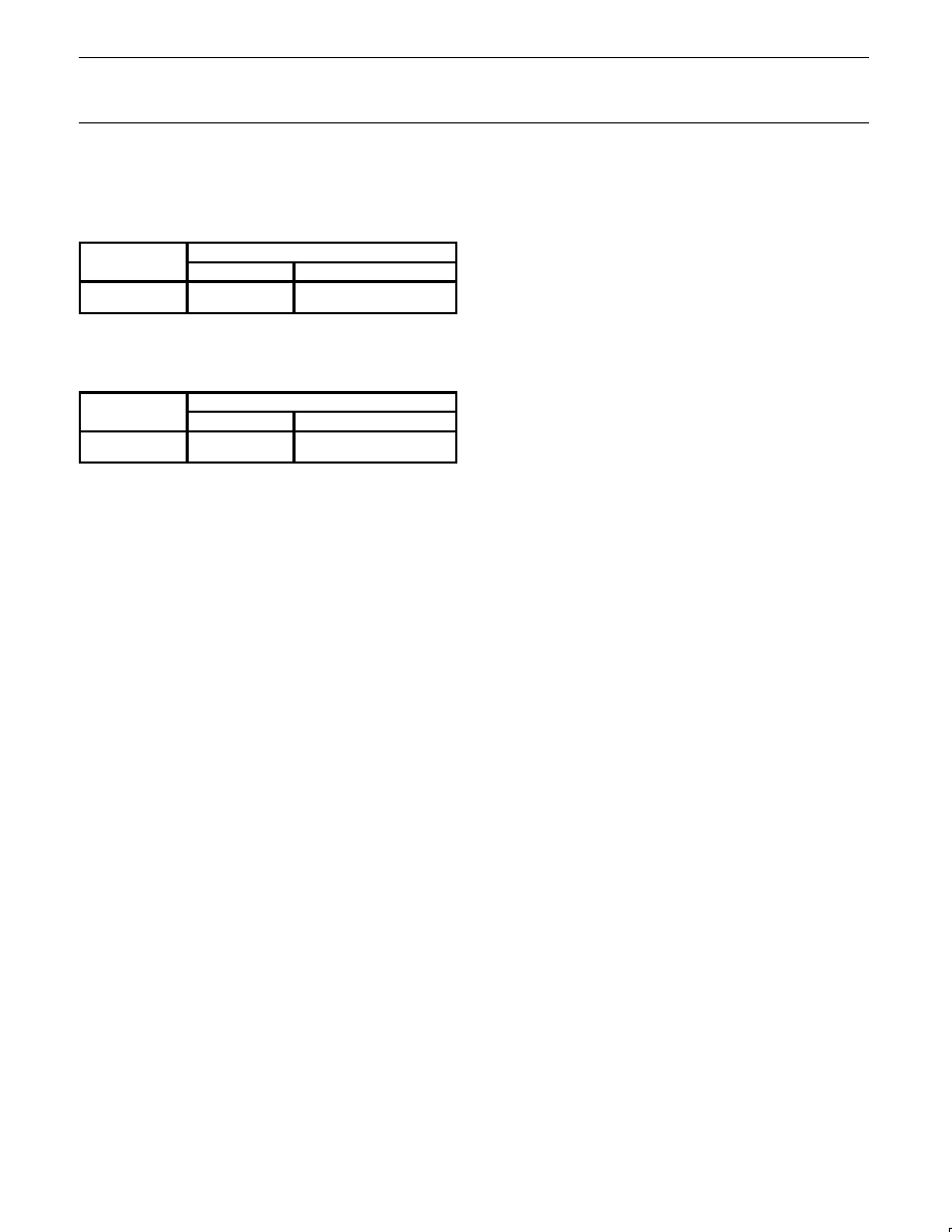
ORDERING INFORMATION
Type number
Package
Name
Description
Version
Commercial;
V
CC
= +5 V
±
5%; T
amb
= 0
∞
C to +70
∞
C
SCC68681C1A44
PLCC44
plastic leaded chip carrier; 44 leads
SOT187-2
SCC68681C1N40
DIP40
plastic dual in-line package; 40 leads (600 mil)
SOT129-1
Industrial;
V
CC
= +5 V
±
10%; T
amb
= ≠40
∞
C to +85
∞
C
SCC68681E1A44
PLCC44
plastic leaded chip carrier; 44 leads
SOT187-2
SCC68681E1N40
DIP40
plastic dual in-line package; 40 leads (600 mil)
SOT129-1
Philips Semiconductors
Product data
SCC68681
Dual asynchronous receiver/transmitter (DUART)
2004 Apr 06
3
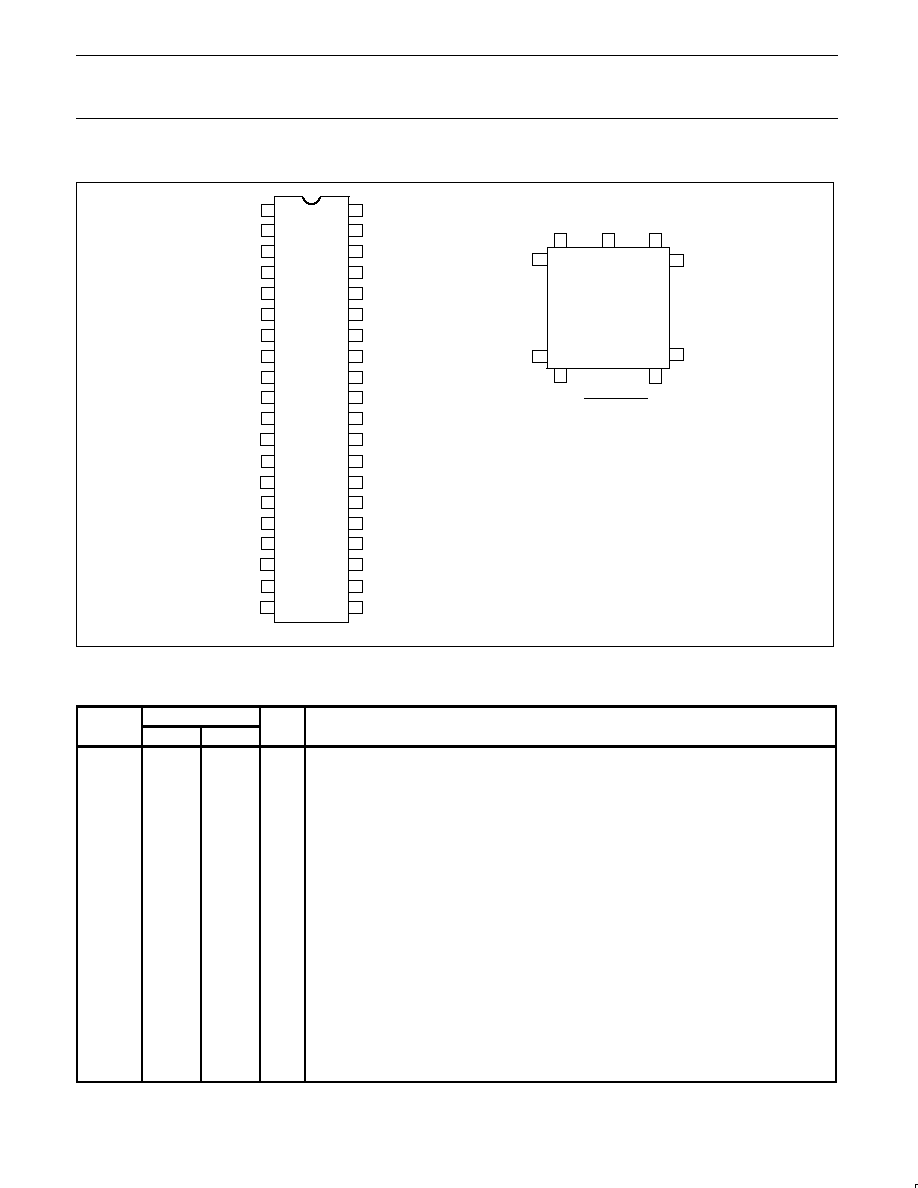
PIN CONFIGURATIONS
1
39
17
28
40
29
18
7
PLCC
6
PIN/FUNCTION
1
NC
16 OP5
31 OP2
2
A1
17 OP7
32 OP0
3
IP3
18 D1
33 TxDA
4
A2
19 D3
34 NC
5
IP1
20 D5
35 RxDA
6
A3
21 D7
36 X1/CLK
7
A4
22 GND
37 X2
8
IP0
23 NC
38 RESETN
9
R/WN
24 INTRN
39 CSN
10 DTACKN
25 D6
40 IP2
11
RxDB
26 D4
41 IACKN
12 NC
27 D2
42 IP5
13 TxDB
28 D0
43 IP4
14 OP1
29 OP6
44 V
CC
15 OP3
30 OP4
24
23
22
21
20
19
18
17
16
15
28
27
12
10
11
9
8
7
6
5
4
3
2
1
14
13
26
25
29
30
31
32
33
34
35
36
37
38
39
40
DIP
VCC
IP4
IP5
IACKN
IP2
CSN
RESETN
X2
X1/CLK
RxDA
TxDA
OP0
OP2
OP4
OP6
D0
D2
D4
D6
INTRN
A1
IP3
A2
IP1
A3
A4
IP0
R/WN
DTACKN
RxDB
TxDB
OP1
OP3
OP5
OP7
D1
D3
D5
D7
GND
SD00107
Figure 1. Pin Configurations
PIN DESCRIPTION
SYMBOL
PIN
TYPE
NAME AND FUNCTION
PLCC44
DIP40
D0≠D7
28, 18,
27, 19,
26, 20,
25, 21
25, 16,
24, 17,
23, 18,
22, 19
I/O
Data Bus: Bidirectional 3-State data bus used to transfer commands, data and status between
the DUART and the CPU. D0 is the least significant bit.
CSN
39
35
I
Chip Select: Active-LOW input signal. When LOW, data transfers between the CPU and the
DUART are enabled on D0≠D7 as controlled by the R/WN, RDN and A1≠A4 inputs. When HIGH,
places the D0≠D7 lines in the 3-State condition.
R/WN
9
8
I
Read/Write: A HIGH input indicates a read cycle and a LOW input indicates a write cycle, when a
cycle is initiated by assertion of the CSN input.
A1≠A4
2, 4, 6, 7
1, 3, 5, 6
I
Address Inputs: Select the DUART internal registers and ports for read/write operations.
RESETN
38
34
I
Reset: A LOW level clears internal registers (SRA, SRB, IMR, ISR, OPR, OPCR), initializes the
IVR to hex 0F, puts OP0≠OP7 in the HIGH state, stops the counter/timer, and puts Channel A and
B in the inactive state, with the TxDA and TxDB outputs in the mark (HIGH) state. Clears Test
modes, sets MR pointer to MR1.
DTACKN
10
9
O
Data Transfer Acknowledge: Three-state active LOW output asserted in write, read, or interrupt
cycles to indicate proper transfer of data between the CPU and the DUART.
INTRN
24
21
O
Interrupt Request: Active-LOW, open-drain, output which signals the CPU that one or more of
the eight maskable interrupting conditions are true.
IACKN
41
37
I
Interrupt Acknowledge: Active-LOW input indicating an interrupt acknowledge cycle. In
response, the DUART will place the interrupt vector on the data bus and will assert DTACKN if it
has an interrupt pending.

Philips Semiconductors
Product data
SCC68681
Dual asynchronous receiver/transmitter (DUART)
2004 Apr 06
4
SYMBOL
NAME AND FUNCTION
TYPE
PIN
SYMBOL
NAME AND FUNCTION
TYPE
DIP40
PLCC44
X1/CLK
36
32
I
Crystal 1: Crystal connection or an external clock input. A crystal of a clock the appropriate
frequency (nominally 3.6864 MHz) must be supplied at all times. For crystal connections see
Figure 8, Clock Timing.
X2
37
33
I
Crystal 2: Crystal connection. See Figure 8. If a crystal is not used it is best to keep this pin not
connected. It must not be grounded.
RxDA
35
31
I
Channel A Receiver Serial Data Input: The least significant bit is received first. `Mark' is HIGH,
`space' is LOW.
RxDB
11
10
I
Channel B Receiver Serial Data Input: The least significant bit is received first. `Mark' is HIGH,
`space' is LOW.
TxDA
33
30
O
Channel A Transmitter Serial Data Output: The least significant bit is transmitted first. This
output is held in the `mark' condition when the transmitter is disabled, idle or when operating in
local loopback mode. `Mark' is HIGH, `space' is LOW.
TxDB
13
11
O
Channel B Transmitter Serial Data Output: The least significant bit is transmitted first. This
output is held in the `mark' condition when the transmitter is disabled, idle, or when operating in
local loopback mode. `Mark' is HIGH, `space' is LOW.
OP0
32
29
O
Output 0: General purpose output or Channel A request to send (RTSAN, active-LOW). Can be
deactivated automatically on receive or transmit.
OP1
14
12
O
Output 1: General purpose output or Channel B request to send (RTSBN, active-LOW). Can be
deactivated automatically on receive or transmit.
OP2
31
28
O
Output 2: General purpose output, or Channel A transmitter 1
◊
or 16
◊
clock output, or Channel A
receiver 1
◊
clock output.
OP3
15
13
O
Output 3: General purpose output or open-drain, active-LOW counter/timer interrupt output or
Channel B transmitter 1
◊
clock output, or Channel B receiver 1
◊
clock output.
OP4
30
27
O
Output 4: General purpose output or Channel A open-drain, active-LOW, RxRDYA/FFULLA
interrupt output.
OP5
16
14
O
Output 5: General purpose output or Channel B open-drain, active-LOW, RxRDYB/FFULLB
interrupt output.
OP6
29
26
O
Output 6: General purpose output or Channel A open-drain, active-LOW, TxRDYA interrupt
output.
OP7
17
15
O
Output 7: General purpose output, or Channel B open-drain, active-LOW, TxRDYB interrupt
output.
IP0
8
7
I
Input 0: General purpose input or Channel A clear to send active-LOW input (CTSAN). Pin has
an internal V
CC
pull-up device supplying 1 to 4
µ
A of current.
IP1
5
4
I
Input 1: General purpose input or Channel B clear to send active-LOW input (CTSBN). Pin has
an internal V
CC
pull-up device supplying 1 to 4
µ
A of current.
IP2
40
36
I
Input 2: General purpose input, or Channel B receiver external clock input (RxCB), or
counter/timer external clock input. When the external clock is used by the receiver, the received
data is sampled on the rising edge of the clock. Pin has an internal V
CC
pull-up device supplying
1 to 4
µ
A of current.
IP3
3
2
I
Input 3: General purpose input or Channel A transmitter external clock input (TxCA). When the
external clock is used by the transmitter, the transmitted data is clocked on the falling edge of the
clock. Pin has an internal V
CC
pull-up device supplying 1 to 4
µ
A of current.
IP4
43
39
I
Input 4: General purpose input or Channel A receiver external clock input (RxCA). When the
external clock is used by the receiver, the received data is sampled on the rising edge of the
clock. Pin has an internal V
CC
pull-up device supplying 1 to 4
µ
A of current.
IP5
42
38
I
Input 5: General purpose input or Channel B transmitter external clock input (TxCB). When the
external clock is used by the transmitter, the transmitted data is clocked on the falling edge of the
clock. Pin has an internal V
CC
pull-up device supplying 1 to 4
µ
A of current.
V
CC
44
40
I
Power Supply: +5 V supply input.
GND
22
20
I
Ground.
NC
1, 12,
23, 34
≠
≠
Not connected.
Philips Semiconductors
Product data
SCC68681
Dual asynchronous receiver/transmitter (DUART)
2004 Apr 06
5
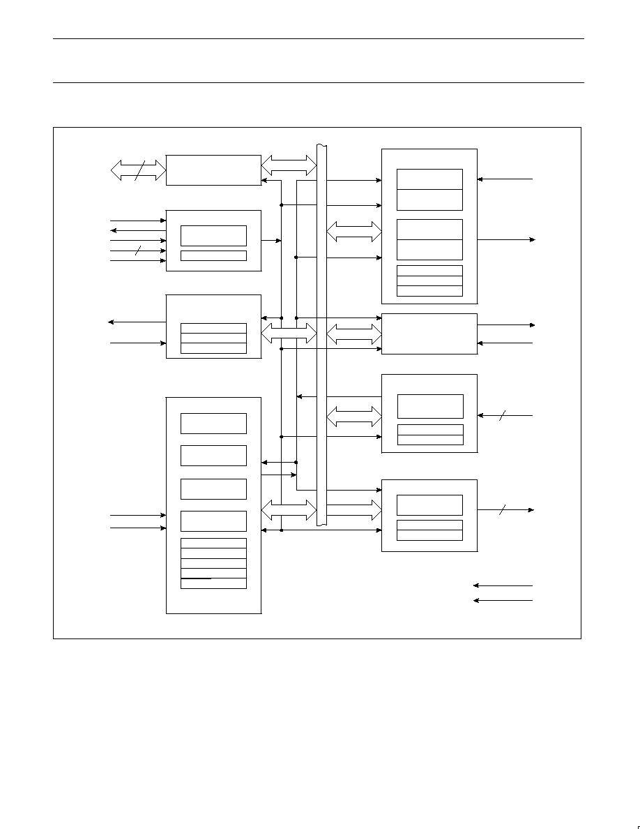
BLOCK DIAGRAM
8
D0≠D7
R/WN
DTACKN
CSN
A1≠A4
RESETN
INTRN
X1/CLK
X2
4
BUS BUFFER
OPERATION CONTROL
ADDRESS
DECODE
R/W CONTROL
INTERRUPT CONTROL
IMR
ISR
TIMING
BAUD RATE
GENERATOR
CLOCK
SELECTORS
COUNTER/
TIMER
XTAL OSC
CSRA
CSRB
ACR
CTLR
CHANNEL A
TRANSMIT
HOLDING REG
TRANSMIT
SHIFT REGISTER
RECEIVE
HOLDING REG (3)
RECEIVE
SHIFT REGISTER
MR1, 2
CRA
SRA
INPUT PORT
CHANGE OF
STATE
DETECTORS (4)
OUTPUT PORT
FUNCTION
SELECT LOGIC
OPCR
TxDA
RxDA
IP0-IP5
OP0-OP7
VCC
GND
CONTROL
TIMING
INTERNAL
DA
T
ABUS
IVR
CHANNEL B
(AS ABOVE)
IPCR
ACR
OPR
CTLR
U
IACKN
RxDB
TxDB
8
6
SD00108
Figure 2. Block Diagram

Philips Semiconductors
Product data
SCC68681
Dual asynchronous receiver/transmitter (DUART)
2004 Apr 06
6
BLOCK DIAGRAM
The SCC68681 DUART consists of the following eight major
sections: data bus buffer, operation control, interrupt control, timing,
communications Channels A and B, input port and output port. Refer
to Figure 2, `Block Diagram'.
Data Bus Buffer
The data bus buffer provides the interface between the external and
internal data buses. It is controlled by the operation control block to
allow read and write operations to take place between the controlling
CPU and the DUART.
Operation Control
The operation control logic receives operation commands from the
CPU and generates appropriate signals to internal sections to
control device operation. It contains address decoding and read and
write circuits to permit communications with the microprocessor via
the data bus buffer. The DTACKN output is asserted during write
and read cycles to indicate to the CPU that data has been latched
on a write cycle, or that valid data is present on the bus on a read
cycle.
Interrupt Control
A single active-LOW interrupt output (INTRN) is provided which is
activated upon the occurrence of any of eight internal events.
Associated with the interrupt system are the Interrupt Mask Register
(IMR) and the Interrupt Status Register (ISR), the Auditory Control
Register(ACR) and the Interrupt Vector Register (IVR). The IMR
may be programmed to select only certain conditions to cause
INTRN to be asserted. The ISR can be read by the CPU to
determine all currently active interrupting conditions. When IACKN is
asserted, and the DUART has an interrupt pending, the DUART
responds by placing the contents of the IVR register on the data bus
and asserting DTACKN.
Outputs OP3≠OP7 can be programmed to provide discrete interrupt
outputs for the transmitter, receivers, and counter/timer.
Timing Circuits
The timing block consists of a crystal oscillator, a baud rate
generator, a programmable 16-bit counter/timer, and four clock
selectors. The crystal oscillator operates directly from a crystal
connected across the X1/CLK and X2 inputs. If an external clock of
the appropriate frequency is available, it may be connected to
X1/CLK. The clock serves as the basic timing reference for the Baud
Rate Generator (BRG), the counter/timer, and other internal circuits.
A clock signal within the limits specified in the specifications section
of this data sheet must always be supplied to the DUART. If an
external is used instead of a crystal, X1 should be driven using a
configuration similar to the one in Figure 8.
The baud rate generator operates from the oscillator or external
clock input and is capable of generating 18 commonly used data
communications baud rates ranging from 50 to 115.2 k baud. The
clock outputs from the BRG are at 16
◊
the actual baud rate. The
counter/timer can be used as a timer to produce a 16
◊
clock for any
other baud rate by counting down the crystal clock or an external
clock. The four clock selectors allow the independent selection, for
each receiver and transmitter, of any of these baud rates or external
timing signal.
Counter/Timer (C/T)
The counter timer is a 16 bit programmable divider that operates
one of three modes: Counter, Timer or Time Out mode. In all three
modes it uses the 16-bit value loaded to the CTUR and CTLR
registers. (Counter timer upper and lower preset registers).
∑
In the timer mode it generates a square wave.
∑
In the counter mode it generates a time delay.
∑
In the time out mode it monitors the receiver data flow and signals
data flow has paused. In the time out mode the receiver controls
the starting/stopping of the C/T.
The counter operates as a down counter and sets its output bit in
the ISR (Interrupt Status Register) each time it passes through 0.
The output of the counter/timer may be seen on one of the OP pins
or as an Rx or Tx clock.
The Timer/Counter is controlled with six (6) `commands'; Start C/T,
Stop C/T, write C/T, preset registers, read C/T value, set or reset
time out mode.
Please see the detail of the commands under the Counter/Timer
register descriptions.
Communications Channels A and B
Each communications channel of the SCC68681 comprises a
full-duplex asynchronous receiver/transmitter (DUART). The
operating frequency for each receiver and transmitter can be
selected independently from the baud rate generator, the counter
timer, or from an external input.
The transmitter accepts parallel data from the CPU, converts it to a
serial bit stream, inserts the appropriate start, stop, and optional
parity bits and outputs a composite serial stream of data on the TxD
output pin. The receiver accepts serial data on the RxD pin,
converts this serial input to parallel format, checks for start bit, stop
bit, parity bit (if any), or break condition and sends an assembled
character to the CPU.
The input port pulse detection circuitry uses a 38.4 kHz sampling
clock derived from one of the baud rate generator taps. This results
in a sampling period of slightly more than 25
µ
s (assuming that the
clock input is 3.6864 MHz). The detection circuitry, in order to
guarantee a true change in level has occurred, requires that two
successive samples at the new logic level be observed. As a
consequence, the minimum duration of the signal change is 25
µ
s if
the transition occurs coincident with the first sample pulse. The
50
µ
s time refers to the situation in which the change of state is just
missed and the first change of state is not detected until 25
µ
s later.
Input Port
The inputs to this unlatched 6-bit port can be read by the CPU by
performing a read operation at address 0xD. A HIGH input results in
a logic `1' while a LOW input results in a logic `0'. D7 will always
read as a logic `1' and D6 will reflect the level of IACKN. The pins of
this port can also serve as auxiliary inputs to certain portions of the
DUART logic.
Four change-of-state detectors are provided which are associated
with inputs IP3, IP2, IP1 and IP0. A HIGH-to-LOW or LOW-to-HIGH
transition of these inputs, lasting longer than 25 to 50
µ
s, will set the
corresponding bit in the input port change register. The bits are
cleared when the register is read by the CPU. Any change-of-state
can also be programmed to generate an interrupt to the CPU.
All the IP pins have a small pull-up device that will source 1 to 4
µ
A
of current from V
CC
. These pins do not require pull-up devices or
V
CC
connections if they are not used.
Output Port
The 8-bit multipurpose output port can be used as a general
purpose output port, in which case the outputs are the complements
of the Output Port Register (OPR). OPR[n] = 1 results in
OP[n] = LOW and vice versa. Bits of the OPR can be individually set
and reset. A bit is set by performing a write operation at address
0xE with the accompanying data specifying the bits to be reset
(1 = set, 0 = no change). Likewise, a bit is reset by a write at

Philips Semiconductors
Product data
SCC68681
Dual asynchronous receiver/transmitter (DUART)
2004 Apr 06
7
address 0xF with the accompanying data specifying the bits to be
reset (1 = reset, 0 = no change).
Outputs can be also individually assigned specific functions by
appropriate programming of the Channel A mode registers (MR1A,
MR2A), the Channel B mode registers (MR1B, MR2B), and the
Output Port Configuration Register (OPCR).
Please note that these pins drive both HIGH and LOW. However,
when they are programmed to represent interrupt type functions
(such as receiver ready, transmitter ready or counter/timer ready)
they will be switched to an open drain configuration in which case an
external pull-up device would be required.
OPERATION
Transmitter
The SCC68681 is conditioned to transmit data when the transmitter
is enabled through the command register. The SCC68681 indicates
to the CPU that it is ready to accept a character by setting the
TxRDY bit in the status register. This condition can be programmed
to generate an interrupt request at OP6 or OP7 and INTRN. When a
character is loaded into the Transmit Holding Register (THR), the
above conditions are negated. Data is transferred from the holding
register to transmit shift register when it is idle or has completed
transmission of the previous character. The TxRDY conditions are
then asserted again which means one full character time of buffering
is provided. Characters cannot be loaded into the THR while the
transmitter is disabled.
The transmitter converts the parallel data from the CPU to a serial
bit stream on the TxD output pin. It automatically sends a start bit
followed by the programmed number of data bits, an optional parity
bit, and the programmed number of stop bits. The least significant
bit is sent first. Following the transmission of the stop bits, if a new
character is not available in the THR, the TxD output remains HIGH
and the TxEMT bit in the Status Register (SR) will be set to 1.
Transmission resumes and the TxEMT bit is cleared when the CPU
loads a new character into the THR.
If the transmitter is disabled, it continues operating until the
character currently being transmitted is completely sent out. The
transmitter can be forced to send a continuous LOW condition by
issuing a send break command.
The transmitter can be reset through a software command (0x30).
If it is reset, operation ceases immediately and the transmitter must
be enabled through the command register before resuming
operation. If CTS operation is enable, the CTSN input must be LOW
in order for the character to be transmitted. If it goes HIGH in the
middle of a transmission, the character in the shift register is
transmitted and TxDA then remains in the marking state until CTSN
goes LOW. The transmitter can also control the deactivation of the
RTSN output. If programmed, the RTSN output will be reset one bit
time after the character in the transmit shift register and transmit
holding register (if any) are completely transmitted, if the transmitter
has been disabled.
Receiver
The SCC68681 is conditioned to receive data when enabled through
the command register. The receiver looks for a HIGH-to-LOW
(mark-to-space) transition of the start bit on the RxD input pin. If a
transition is detected, the state of the RxD pin is sampled each 16
◊
clock for 7-
1
/
2
clocks (16
◊
clock mode) or at the next rising edge of
the bit time clock (1
◊
clock mode). If RxD is sampled HIGH, the start
bit is invalid and the search for a valid start bit begins again. If RxD
is still LOW, a valid start bit is assumed and the receiver continues
to sample the input at one bit time intervals at the theoretical center
of the bit, until the proper number of data bits and parity bit (if any)
have been assembled, and one stop bit has been detected. The
least significant bit is received first. The data is then transferred to
the Receive Holding Register (RHR) and the RxRDY bit in the SR is
set to a `1'. This condition can be programmed to generate an
interrupt at OP4 or OP5 and INTRN. If the character length is less
than 8 bits, the most significant unused bits in the RHR are set to
zero.
After the stop bit is detected, the receiver will immediately look for
the next start bit. However, if a non-zero character was received
without a stop bit (framing error) and RxD remains LOW for one half
of the bit period after the stop bit was sampled, then the receiver
operates as if a new start bit transition had been detected at that
point (one-half bit time after the stop bit was sampled).
The parity error, framing error, and overrun error (if any) are strobed
into the SR at the received character boundary, before the RxRDY
status bit is set. If a break condition is detected (RxD is LOW for the
entire character including the stop bit), a character consisting of all
zeros will be loaded into the RHR and the received break bit in the
SR is set to `1'. The RxD input must return to HIGH for two (2) clock
edges of the X1 crystal clock for the receiver to recognize the end of
the break condition and begin the search for a start bit. This will
usually require a HIGH time of one X1 clock period or 3 X1
edges since the clock of the controller is not synchronous to
the X1 clock.
Receiver FIFO
The RHR consists of a First-In-First-Out (FIFO) stack with a
capacity of three characters. Data is loaded from the receive shift
register into the top most empty position of the FIFO. The RxRDY bit
in the status register is set whenever one or more characters are
available to be read, and a FFULL status bit is set if all three stack
positions are filled with data. Either of these bits can be selected to
cause an interrupt. A read of the RHR outputs the data at the top of
the FIFO. After the read cycle, the data FIFO and its associated
status bits (see below) are `popped' thus emptying a FIFO position
for new data.
Receiver Status Bits
In addition to the data word, three status bits (parity error, framing
error, and received break) are also appended to each data character
in the FIFO (overrun is not). Status can be provided in two ways, as
programmed by the error mode control bit in the mode register. In
the `character' mode, status is provided on a character-by-character
basis; the status applies only to the character at the top of the FIFO.
In the `block' mode, the status provided in the SR for these three bits
is the logical-OR of the status for all characters coming to the top of
the FIFO since the last `reset error' command was issued. In either
mode reading the SR does not affect the FIFO. The FIFO is
`popped' only when the RHR is read. Therefore the status register
should be read prior to reading the FIFO.
If the FIFO is full when a new character is received, that character is
held in the receive shift register until a FIFO position is available. If
an additional character is received while this state exits, the
contents of the FIFO are not affected; the character previously in the
shift register is lost and the overrun error status bit (SR[4]) will be
set upon receipt of the start bit of the new (overrunning) character).
The receiver can control the deactivation of RTS. If programmed to
operate in this mode, the RTSN output will be negated (set to `1')
when a valid start bit was received and the FIFO is full. When a
FIFO position becomes available, the RTSN output will be

Philips Semiconductors
Product data
SCC68681
Dual asynchronous receiver/transmitter (DUART)
2004 Apr 06
8
re-asserted (set to `0') automatically. This feature can be used to
prevent an overrun, in the receiver, by connecting the RTSN output
to the CTSN input of the transmitting device.
Receiver Reset and Disable
Receiver disable stops the receiver immediately ≠ data being
assembled if the receiver shift register is lost. Data and status in the
FIFO is preserved and may be read. A re-enable of the receiver after
a disable will cause the receiver to begin assembling characters at the
next start bit detected. A receiver reset will discard the present shift
register data, reset the receiver ready bit (RxRDY), clear the status of
the byte at the top of the FIFO and re-align the FIFO read/write
pointers. This has the appearance of `clearing or flushing' the receiver
FIFO. In fact, the FIFO is NEVER cleared! The data in the FIFO
remains valid until overwritten by another received character. Because
of this, erroneous reading or extra reads of the receiver FIFO will
mis-align the FIFO pointers and result in the reading of previously
read data. A receiver reset will re-align the pointers.
Multidrop Mode
The DUART is equipped with a wake up mode for multidrop
applications. This mode is selected by programming bits MR1A[4:3] or
MR1B[4:3] to `11' for Channels A and B, respectively. In this mode of
operation, a `master' station transmits an address character followed by
data characters for the addressed `slave' station. The slave stations, with
receivers that are normally disabled, examine the received data stream
and `wake up' the CPU (by setting RxRDY) only upon receipt of an
address character. The CPU compares the received address to its
station address and enables the receiver if it wishes to receive the
subsequent data characters. Upon receipt of another address character,
the CPU may disable the receiver to initiate the process again.
A transmitted character consists of a start bit, the programmed
number of data bits, and Address/Data (A/D) bit, and the
programmed number of stop bits. The polarity of the transmitted A/D
bit is selected by the CPU by programming bit MR1A[2]/MR1B[2].
MR1A[2]/MR1B[2] = 0 transmits a zero in the A/D bit position, which
identifies the corresponding data bits as data while
MR1A[2]/MR1B[2] = 1 transmits a one in the A/D bit position, which
identifies the corresponding data bits as an address. The CPU
should program the mode register prior to loading the corresponding
data bits into the THR.
In this mode, the receiver continuously looks at the received data
stream, whether it is enabled or disabled. If disabled, it sets the
RxRDY status bit and loads the character into the RHR FIFO if the
received A/D bit is a one (address tag), but discards the received
character if the received A/D bit is a zero (data tag). If enabled, all
received characters are transferred to the CPU via the RHR. In
either case, the data bits are loaded into the data FIFO while the
A/D bit is loaded into the status FIFO position normally used for
parity error (SRA[5] or SRB[5]). Framing error, overrun error, and
break detect operate normally whether or not the receive is enabled.
PROGRAMMING
The operation of the DUART is programmed by writing control words
into the appropriate registers. Operational feedback is provided via
status registers which can be read by the CPU. The addressing of
the registers is described in Table 1.
The contents of certain control registers are initialized to zero on
RESETN. Care should be exercised if the contents of a register are
changed during operation, since certain changes may cause
operational problems.
For example, changing the number of bits per character while the
transmitter is active may cause the transmission of an incorrect
character. In general, the contents of the MR, the CSR, and the
OPCR should only be changed while the receiver(s) and
transmitter(s) are not enabled, and certain changes to the ACR
should only be made while the C/T is stopped.
Mode registers 1 and 2 of each channel are accessed via
independent auxiliary pointers. The pointer is set to MR1x by RESET
or by issuing a `reset pointer' command via the corresponding
command register. Any read or write of the mode register while the
pointer is at MR1x, switches the pointer to MR2x. The pointer then
remains at MR2x, so that subsequent accesses are always to MR2x
unless the pointer is reset to MR1x as described above.
Mode, command, clock select, and status registers are duplicated
for each channel to provide total independent operation and control.
Refer to Table 2 for register bit descriptions.
Table 1.
SCC68681 Register Addressing
A4
A3
A2
A1
READ (R/WN = 1)
WRITE (R/WN = 0)
0
0
0
0
Mode Register A (MR1A, MR2A)
Mode Register A (MR1A, MR2A)
0
0
0
1
Status Register A (SRA)
Clock Select Register A (CSRA)
0
0
1
0
BRG Test
Command Register A (CRA)
0
0
1
1
Rx Holding Register A (RHRA)
Tx Holding Register A (THRA)
0
1
0
0
Input Port Change Register (IPCR)
Aux. Control Register (ACR)
0
1
0
1
Interrupt Status Register (ISR)
Interrupt Mask Register (IMR)
0
1
1
0
Counter/Timer Upper Value (CTU)
C/T Upper Preset Value (CRUR)
0
1
1
1
Counter/Timer Lower Value (CTL)
C/T Lower Preset Value (CTLR)
1
0
0
0
Mode Register B (MR1B, MR2B)
Mode Register B (MR1B, MR2B)
1
0
0
1
Status Register B (SRB)
Clock Select Register B (CSRB)
1
0
1
0
1
◊
/16
◊
Test
Command Register B (CRB)
1
0
1
1
Rx Holding Register B (RHRB)
Tx Holding Register B (THRB)
1
1
0
0
Interrupt Vector Register (IVR)
Interrupt Vector Register (IVR)
1
1
0
1
Input Ports IP0 to IP6
Output Port Conf. Register (OPCR)
1
1
1
0
Start Counter Command
Set Output Port Bits Command
1
1
1
1
Stop Counter Command
Reset Output Port Bits Command
* See Table 6 for BRG Test frequencies in this data sheet, and
"Extended baud rates for SCN2681, SCN68681, SCC2691, SCC2692,
SCC68681 and SCC2698B" in application notes elsewhere in this publication
Philips Semiconductors
Product data
SCC68681
Dual asynchronous receiver/transmitter (DUART)
2004 Apr 06
9
Table 2.
Register Bit Formats
BIT 7
BIT 6
BIT 5
BIT 4 BIT 3
BIT 2
BIT 1 BIT 0
MR1A
RxRTS
CONTROL
RxINT
SELECT
ERROR
MODE*
PARITY MODE
PARITY
TYPE
BITS PER
CHARACTER
MR1A
MR1B
0 = No
1 = Yes
0 = RxRDY
1 = FFULL
0 = Char
1 = Block
00 = With Parity
01 = Force Parity
10 = No Parity
11 = Multidrop Mode**
0 = Even
1 = Odd
00 = 5
01 = 6
10 = 7
11 = 8
NOTE:
* In block error mode, block error conditions must be cleared by using the error reset command (command 4x) or a receiver reset.
** Please see Receiver Reset note on page 19.
BIT 7 BIT 6
BIT 5
BIT 4
BIT 3 BIT 2 BIT 1 BIT 0
MR2A
CHANNEL MODE
TxRTS
CONTROL
CTS
ENABLE Tx
STOP BIT LENGTH*
MR2A
MR2B
00 = Normal
01 = Auto-Echo
10 = Local loop
11 = Remote loop
0 = No
1 = Yes
0 = No
1 = Yes
0 = 0.563
4 = 0.813
8 = 1.563
C = 1.813
1 = 0.625
5 = 0.875
9 = 1.625
D = 1.875
2 = 0.688
6 = 0.938
A = 1.688
E = 1.938
3 = 0.750
7 = 1.000
B = 1.750
F = 2.000
NOTE:
*Add 0.5 to values shown for 0 - 7 if channel is programmed for 5 bits/char.
CSRA
BIT 7 BIT 6 BIT 5 BIT 4
BIT 3 BIT 2 BIT 1 BIT 0
CSRA
CSRB
RECEIVER CLOCK SELECT
TRANSMITTER CLOCK SELECT
CSRB
See Text
See Text
NOTE:
* See Table 6 for BRG Test frequencies in this data sheet, and
"Extended baud rates for SCN2681, SCN68681, SCC2691, SCC2692,
SCC68681 and SCC2698B" in application notes elsewhere in this publication
BIT 7
BIT 6 BIT 5 BIT 4
BIT 3
BIT 2
BIT 1
BIT 0
CRA
CRB
MISCELLANEOUS COMMANDS
DISABLE Tx
ENABLE Tx
DISABLE Rx
ENABLE Rx
CRB
Not used ≠
must be 0
See Text
0 = No
1 = Yes
0 = No
1 = Yes
0 = No
1 = Yes
0 = No
1 = Yes
NOTE:
*Access to the upper four bits of the command register should be separated by three (3) edges of the X1 clock. A disabled transmitter cannot
be loaded. For Rx and Tx performing a Disable and Enable at the same time results in Disable.
BIT 7
BIT 6
BIT 5
BIT 4
BIT 3
BIT 2
BIT 1
BIT 0
SRA
SRB
RECEIVED
BREAK*
FRAMING
ERROR*
PARITY
ERROR*
OVERRUN
ERROR
TxEMT
TxRDY
FFULL
RxRDY
SRB
0 = No
1 = Yes
0 = No
1 = Yes
0 = No
1 = Yes
0 = No
1 = Yes
0 = No
1 = Yes
0 = No
1 = Yes
0 = No
1 = Yes
0 = No
1 = Yes
NOTE:
*These status bits are appended to the corresponding data character in the receive FIFO. A read of the status provides these bits (7:5) from the
top of the FIFO together with bits (4:0). These bits are cleared by a `reset error status' command. In character mode they are discarded when
the corresponding data character is read from the FIFO. In block error mode, block error conditions must be cleared by using the error reset
command (command 4x) or a receiver reset.
BIT 7
BIT 6
BIT 5
BIT 4
BIT 3 BIT 2
BIT 1 BIT 0
OP7
OP6
OP5
OP4
OP3
OP2
OPCR
0 = OPR[7]
1 = TxRDYB
0 = OPR[6]
1 = TxRDYA
0 = OPR[5]
1 = RxRDY/
FFULLB
0 = OPR[4]
1 = RxRDY/
FFULLA
00 = OPR[3]
01 = C/T OUTPUT
10 = TxCB(1
◊
)
11 = RxCB(1
◊
)
00 = OPR[2]
01 = TxCA(16
◊
)
10 = TxCA(1
◊
)
11 = RxCA(1
◊
)
OPR
BIT 7
BIT 6
BIT 5
BIT 4
BIT 3
BIT 2
BIT 1
BIT 0
OPR bit
0
1
0
1
0
1
0
1
0
1
0
1
0
1
0
1
OP pin
1
0
1
0
1
0
1
0
1
0
1
0
1
0
1
0
NOTE:
The level at the OP pin is the inverse of the bit in the OPR register.
Philips Semiconductors
Product data
SCC68681
Dual asynchronous receiver/transmitter (DUART)
2004 Apr 06
10
Table 2. Register Bit Formats
(Continued)
BIT 7
BIT 6 BIT 5 BIT 4
BIT 3
BIT 2
BIT 1
BIT 0
ACR
BRG SET
SELECT
COUNTER/TIMER
MODE AND SOURCE
DELTA
IP3 INT
DELTA
IP2 INT
DELTA
IP1 INT
DELTA
IP0 INT
0 = set 1
1 = set 2
See Table 4
0 = Off
1 = On
0 = Off
1 = On
0 = Off
1 = On
0 = Off
1 = On
BIT 7
BIT 6
BIT 5
BIT 4
BIT 3
BIT 2
BIT 1
BIT 0
IPCR
DELTA
IP3
DELTA
IP2
DELTA
IP1
DELTA
IP0
IP3
IP2
IP1
IP0
0 = No
1 = Yes
0 = No
1 = Yes
0 = No
1 = Yes
0 = No
1 = Yes
0 = LOW
1 = HIGH
0 = LOW
1 = HIGH
0 = LOW
1 = HIGH
0 = LOW
1 = HIGH
BIT 7
BIT 6
BIT 5
BIT 4
BIT 3
BIT 2
BIT 1
BIT 0
ISR
INPUT
PORT
CHANGE
DELTA
BREAK B
RxRDY/
FFULLB
TxRDYB
COUNTER
READY
DELTA
BREAK A
RxRDY/
FFULLA
TxRDYA
0 = No
1 = Yes
0 = No
1 = Yes
0 = No
1 = Yes
0 = No
1 = Yes
0 = No
1 = Yes
0 = No
1 = Yes
0 = No
1 = Yes
0 = No
1 = Yes
BIT 7
BIT 6
BIT 5
BIT 4
BIT 3
BIT 2
BIT 1
BIT 0
IMR
IN. PORT
CHANGE
INT
DELTA
BREAK B
INT
RxRDY/
FFULLB
INT
TxRDYB
INT
COUNTER
READY
INT
DELTA
BREAK A
INT
RxRDY/
FFULLA
INT
TxRDYA
INT
0 = Off
1 = On
0 = Off
1 = On
0 = Off
1 = On
0 = Off
1 = On
0 = Off
1 = On
0 = Off
1 = On
0 = Off
1 = On
0 = Off
1 = On
BIT 7
BIT 6
BIT 5
BIT 4
BIT 3
BIT 2
BIT 1
BIT 0
CTUR
C/T[15]
C/T[14]
C/T[13]
C/T[12]
C/T[11]
C/T[10]
C/T[9]
C/T[8]
BIT 7
BIT 6
BIT 5
BIT 4
BIT 3
BIT 2
BIT 1
BIT 0
CTLR
C/T[7]
C/T[6]
C/T[5]
C/T[4]
C/T[3]
C/T[2]
C/T[1]
C/T[0]
BIT 7
BIT 6
BIT 5
BIT 4
BIT 3
BIT 2
BIT 1
BIT 0
IVR
IVR[7]
IVR[6]
IVR[5]
IVR[4]
IVR[3]
IVR[2]
IVR[1]
IVR[0]
BIT 7
BIT 6
BIT 5
BIT 4
BIT 3
BIT 2
BIT 1
BIT 0
SOPR
OP7
OP6
OP5
OP4
OP3
OP2
OP1
OP0
SOPR
0 =
no change
1 = set bit
0 =
no change
1 = set bit
0 =
no change
1 = set bit
0 =
no change
1 = set bit
0 =
no change
1 = set bit
0 =
no change
1 = set bit
0 =
no change
1 = set bit
0 =
no change
1 = set bit
BIT 7
BIT 6
BIT 5
BIT 4
BIT 3
BIT 2
BIT 1
BIT 0
ROPR
OP7
OP6
OP5
OP4
OP3
OP2
OP1
OP0
ROPR
0 =
no change
1 = reset bit
0 =
no change
1 = reset bit
0 =
no change
1 = reset bit
0 =
no change
1 = reset bit
0 =
no change
1 = reset bit
0 =
no change
1 = reset bit
0 =
no change
1 = reset bit
0 =
no change
1 = reset bit

Philips Semiconductors
Product data
SCC68681
Dual asynchronous receiver/transmitter (DUART)
2004 Apr 06
11
MR1A ≠ Channel A Mode Register 1
MR1A is accessed when the Channel A MR pointer points to MR1.
The pointer is set to MR1 by RESET or by a `set pointer' command
applied via CRA. After reading or writing MR1A, the pointer will point
to MR2A.
MR1A[7] ≠ Channel A Receiver Request-to-Send Control
This bit controls the deactivation of the RTSAN output (OP0) by the
receiver. This output is normally asserted by setting OPR[0] and
negated by resetting OPR[0]. MR1A[7] = 1 causes RTSAN to be
negated upon receipt of a valid start bit if the Channel A FIFO is full.
However, OPR[0] is not reset and RTSAN will be asserted again
when an empty FIFO position is available. This feature can be used
for flow control to prevent overrun in the receiver by using the
RTSAN output signal to control the CTSN input of the transmitting
device.
MR1A[6] ≠ Channel A Receiver Interrupt Select
This bit selects either the Channel A receiver ready status (RxRDY)
or the Channel A FIFO full status (FFULL) to be used for CPU
interrupts. It also causes the selected bit to be output on OP4 if it is
programmed as an interrupt output via the OPCR.
MR1A[5] ≠ Channel A Error Mode Select
This bit select the operating mode of the three FIFOed status bits
(FE, PE, received break) for Channel A. In the `character' mode,
status is provided on a character-by-character basis; the status
applies only to the character at the top of the FIFO. In the `block'
mode, the status provided in the SR for these bits is the
accumulation (logical-OR) of the status for all characters coming to
the top of the FIFO since the last `reset error' command for Channel
A was issued.
MR1A[4:3| ≠ Channel A Parity Mode Select
If `with parity' or `force parity' is selected a parity bit is added to the
transmitted character and the receiver performs a parity check on
incoming data MR1A[4:3] = 11 selects Channel A to operate in the
special multidrop mode described in the Operation section.
MR1A[2] ≠ Channel A Parity Type Select
This bit selects the parity type (odd or even) if the `with parity' mode
is programmed by MR1A[4:3], and the polarity of the forced parity bit
if the `force parity' mode is programmed. It has no effect if the `no
parity' mode is programmed. In the special multidrop mode it selects
the polarity of the A/D bit.
MR1A[1:0] ≠ Channel A Bits Per Character Select
This field selects the number of data bits per character to be
transmitted and received. The character length does not include the
start, parity, and stop bits.
MR2A ≠ Channel A Mode Register 2
MR2A is accessed when the Channel A MR pointer points to MR2,
which occurs after any access to MR1A. Accesses to MR2A do not
change the pointer.
MR2A[7:6] ≠ Channel A Mode Select
Each channel of the DUART can operate in one of four modes.
MR2A[7:6] = 00 is the normal mode, with the transmitter and
receiver operating independently. MR2A[7:6] = 01 places the
channel in the automatic echo mode, which automatically
re-transmits the received data. The following conditions are true
while in automatic echo mode:
1. Received data is re-clocked and re-transmitted on the TxDA
output.
2. The receive clock is used for the transmitter.
3. The receiver must be enabled, but the transmitter need not be
enabled.
4. The Channel A TxRDY and TxEMT status bits are inactive.
5. The received parity is checked, but is not regenerated for
transmission, i.e. transmitted parity bit is as received.
6. Character framing is checked, but the stop bits are retransmitted
as received.
7. A received break is echoed as received until the next valid start
bit is detected.
8. CPU to receiver communication continues normally, but the CPU
to transmitter link is disabled.
Two diagnostic modes can also be configured. MR2A[7:6] = 10
selects local loopback mode. In this mode:
1. The transmitter output is internally connected to the receiver
input.
2. The transmit clock is used for the receiver.
3. The TxDA output is held HIGH.
4. The RxDA input is ignored.
5. The transmitter must be enabled, but the receiver need not be
enabled.
6. CPU to transmitter and receiver communications continue
normally.
The second diagnostic mode is the remote loopback mode, selected
by MR2A[7:6] = 11. In this mode:
1. Received data is re-clocked and re-transmitted on the TxDA
output.
2. The receive clock is used for the transmitter.
3. Received data is not sent to the local CPU, and the error status
conditions are inactive.
4. The received parity is not checked and is not regenerated for
transmission, i.e., transmitted parity is as received.
5. The receiver must be enabled.
6. Character framing is not checked, and the stop bits are
retransmitted as received.
7. A received break is echoed as received until the next valid start
bit is detected.
The user must exercise care when switching into and out of the
various modes. The selected mode will be activated immediately
upon mode selection, even if this occurs in the middle of a received
or transmitted character. Likewise, if a mode is deselected the
device will switch out of the mode immediately. An exception to this
is switching out of autoecho or remote loopback modes: if the
de-selection occurs just after the receiver has sampled the stop bit
(indicated in autoecho by assertion of RxRDY), and the transmitter
is enabled, the transmitter will remain in autoecho mode until the
entire stop has been re-transmitted.
MR2A[5] ≠ Channel A Transmitter Request-to-Send Control
CAUTION: When the transmitter controls the OP pin (usually used
for the RTSN signal) the meaning of the pin is not RTSN at all!
Rather, it signals that the transmitter has finished the transmission
(i.e., end of block).
This bit allows deactivation of the RTSN output by the transmitter.
This output is manually asserted and negated by the appropriate

Philips Semiconductors
Product data
SCC68681
Dual asynchronous receiver/transmitter (DUART)
2004 Apr 06
12
commands issued via the SOPR and ROPR registers. MR2[5] set to
1 caused the RTSN to be reset automatically one bit time after the
character(s) in the transmit shift register and in the THR (if any) are
completely transmitted (including the programmed number of stop
bits) if a previously issued transmitter disable is pending. This
feature can be used to automatically terminate the transmission as
follows:
1. Program the auto-reset mode: MR2[5]=1
2. Enable transmitter, if not already enabled
3. Set OPR[0] or OPR[1] to `1' via SOPR and ROPR.
4. Send message
5. After the last character of the message is loaded to the THR,
disable the transmitter. (If the transmitter is underrun, a special
case exists. See note below.)
6. The last character will be transmitted and the RTSN will be reset
one bit time after the last stop bit is sent.
NOTE: The transmitter is in an underrun condition when both the
TxRDY and the TxEMT bits are set. This condition also exists
immediately after the transmitter is enabled from the disabled or
reset state. When using the above procedure with the transmitter in
the underrun condition, the issuing of the transmitter disable must be
delayed from the loading of a single, or last, character until the
TxRDY becomes active again after the character is loaded.
MR2A[4] ≠ Channel A Clear-to-Send Control
If this bit is 0, CTSAN has no effect on the transmitter. If this bit is a
1, the transmitter checks the state of CTSAN (IP0) each time it is
ready to send a character. If IP0 is asserted (LOW), the character is
transmitted. If it is negated (HIGH), the TxDA output remains in the
marking state and the transmission is delayed until CTSAN goes
LOW. Changes in CTSAN while a character is being transmitted do
not affect the transmission of that character.
MR2A[3:0] ≠ Channel A Stop Bit Length Select
This field programs the length of the stop bit appended to the
transmitted character. Stop bit lengths of 9/16 to 1 and 1-9/16 to 2
bits, in increments of 1/16 bit, can be programmed for character
lengths of 6, 7, and 8 bits. For a character lengths of 5 bits, 1-1/16 to
2 stop bits can be programmed in increments of 1/16 bit. The
receiver only checks for a `mark' condition at the center of the first
stop bit position (one bit time after the last data bit, or after the parity
bit is enabled), in all cases.
If an external 1
◊
clock is used for the transmitter, MR2A[3] = 0
selects one stop bit and MR2A[3] = 1 selects two stop bits to be
transmitted.
MR1B ≠ Channel B Mode Register 1
MR1B is accessed when the Channel B MR pointer points to MR1.
The pointer is set to MR1 by RESET or by a `set pointer' command
applied via CRB. After reading or writing MR1B, the pointer will point
to MR2B.
The bit definitions for this register are identical to MR1A, except that
all control actions apply to the Channel B receiver and transmitter
and the corresponding inputs and outputs.
MR2B ≠ Channel B Mode Register 2
MR2B is accessed when the Channel B MR pointer points to MR2,
which occurs after any access to MR1B. Accesses to MR2B do not
change the pointer.
The bit definitions for mode register are identical to the bit definitions
for MR2A, except that all control actions apply to the Channel B
receiver and transmitter and the corresponding inputs and outputs.
CSRA ≠ Channel A Clock Select Register
CSRA[7:4] ≠ Channel A Receiver Clock Select
This field selects the baud rate clock for the Channel A receiver. The
field definition is shown in Table 3.
CSRA[3:0] ≠ Channel A Transmitter Clock Select
This field selects the baud rate clock for the Channel A transmitter.
The field definition is as shown in Table 3, except as follows:
CSRA[3:0]
Baud Rate
ACR[7] = 0
ACR[7] = 1
1110
1111
IP3≠16
◊
IP3≠1
◊
IP3≠16
◊
IP3≠1
◊
The transmitter and receiver clock is always a 16
◊
clock except
for 1111 selection.
Table 3.
X1 clock = 3.6864 MHz
CSRA[7:4]
Baud Rate
ACR[7] = 0
ACR[7] = 1
0000
50
75
0001
110
110
0010
134.5
134.5
0011
200
150
0100
300
300
0101
600
600
0110
1,200
1,200
0111
1,050
2,000
1000
2,400
2,400
1001
4,800
4,800
1010
7,200
1,800
1011
9,600
9,600
1100
38.4 k
19.2 k
1101
Timer
Timer
1110
IP4≠16
◊
IP4≠16
◊
1111
IP4≠1
◊
IP4≠1
◊
See Table 6 for other rates to 115.2 k baud.
Philips Semiconductors
Product data
SCC68681
Dual asynchronous receiver/transmitter (DUART)
2004 Apr 06
13
CSRB ≠ Channel B Clock Select Register
CSRB[7:4] ≠ Channel B Receiver Clock Select
This field selects the baud rate clock for the Channel B receiver. The
field definition is as shown in Table 3, except as follows:
CSRB[7:4]
Baud Rate
CSRB[7:4]
ACR[7] = 0
ACR[7] = 1
1110
1111
IP2≠16
◊
IP2≠1
◊
IP2≠16
◊
IP2≠1
◊
The receiver clock is always a 16
◊
clock except for CSRB[7:4] = 1111.
CSRB[3:0] ≠ Channel B Transmitter Clock Select
This field selects the baud rate clock for the Channel B transmitter.
The field definition is as shown in Table 3, except as follows:
CSRB[3:0]
Baud Rate
CSRB[3:0]
ACR[7] = 0
ACR[7] = 1
1110
1111
IP5≠16
◊
IP5≠1
◊
IP5≠16
◊
IP5≠1
◊
The transmitter clock is always a 16
◊
clock except for
CSRB[3:0] = 1111.
CRA ≠ Channel A Command Register
CRA is a register used to supply commands to Channel A. Multiple
commands can be specified in a single write to CRA as long as the
commands are non-conflicting, e.g., the `enable transmitter' and
`reset transmitter' commands cannot be specified in a single
command word.
CRA[7] ≠ Not Used
Should be set to zero for upward compatibility with newer parts.
CRA[6:4] ≠ Miscellaneous Commands
The encoded value of this field may be used to specify a single
command as follows:
CRA[6:4] ≠ COMMAND
NOTE: Access to the upper four bits of the command register should
be separated by three (3) edges of the X1 clock.
000
No command.
001
Reset MR pointer. Causes the Channel A MR pointer to point
to MR1.
010
Reset receiver. Resets the Channel A receiver as if a
hardware reset had been applied. The receiver is disabled
and the FIFO is flushed.
011
Reset transmitter. Resets the Channel A transmitter as if a
hardware reset had been applied.
100
Reset error status. Clears the Channel A Received Break,
Parity Error, and Overrun Error bits in the status register
(SRA[7:4]). Used in character mode to clear OE status
(although RB, PE and FE bits will also be cleared) and in
block mode to clear all error status after a block of data has
been received.
101
Reset Channel A break change interrupt. Causes the
Channel A break detect change bit in the interrupt status
register (ISR[2]) to be cleared to zero.
110
Start break. Forces the TxDA output LOW (spacing). If the
transmitter is empty the start of the break condition will be
delayed up to two bit times. If the transmitter is active the
break begins when transmission of the character is
completed. If a character is in the THR, the start of the break
will be delayed until that character, or any other loaded
subsequently are transmitted. The transmitter must be
enabled for this command to be accepted.
111
Stop break. The TxDA line will go HIGH (marking) within two
bit times. TxDA will remain HIGH for one bit time before the
next character, if any, is transmitted.
CRA[3] ≠ Disable Channel A Transmitter
This command terminates transmitter operation and reset the
TxDRY and TxEMT status bits. However, if a character is being
transmitted or if a character is in the THR when the transmitter is
disabled, the transmission of the character(s) is completed before
assuming the inactive state.
CRA[2] ≠ Enable Channel A Transmitter
Enables operation of the Channel A transmitter. The TxRDY status
bit will be asserted.
CRA[1] ≠ Disable Channel A Receiver
This command terminates operation of the receiver immediately ≠ a
character being received will be lost. The command has no effect on
the receiver status bits or any other control registers. If the special
multidrop mode is programmed, the receiver operates even if it is
disabled. See Operation section.
CRA[0] ≠ Enable Channel A Receiver
Enables operation of the Channel A receiver. If not in the special
wake-up mode, this also forces the receiver into the search for
start-bit state.
Note: Performing a Disable and Enable at the same time results in
Disable.
CRB ≠ Channel B Command Register
CRB is a register used to supply commands to Channel B. Multiple
commands can be specified in a single write to CRB as long as the
commands are non-conflicting, e.g., the `enable transmitter' and
`reset transmitter' commands cannot be specified in a single
command word.
The bit definitions for this register are identical to the bit definitions
for CRA, except that all control actions apply to the Channel B
receiver and transmitter and the corresponding inputs and outputs.,
SRA ≠ Channel A Status Register
SRA[7] ≠ Channel A Received Break
This bit indicates that an all zero character of the programmed
length has been received without a stop bit. Only a single FIFO
position is occupied when a break is received further entries to the
FIFO are inhibited until the RxDA line to the marking state for at
least one-half a bit time two successive edges of the internal or
external 1
◊
clock. This will usually require a HIGH time of one X1
clock period or 3 X1 edges since the clock of the controller is
not synchronous to the X1 clock.
When this bit is set, the Channel A `change in break' bit in the ISR
(ISR[2]) is set. ISR[2] is also set when the end of the break
condition, as defined above, is detected.
The break detect circuitry can detect breaks that originate in the
middle of a received character. However, if a break begins in the
middle of a character, it must persist until at least the end of the next
character time in order for it to be detected.
SRA[6] ≠ Channel A Framing Error
This bit, when set, indicates that a stop bit was not detected when
the corresponding data character in the FIFO was received. The
stop bit check is made in the middle of the first stop bit position.
SRA[5] ≠ Channel A Parity Error
This bit is set when the `with parity' or `force parity' mode is
programmed and the corresponding character in the FIFO was
received with incorrect parity.
In the special multidrop mode the parity error bit stores the receive
A/D bit.

Philips Semiconductors
Product data
SCC68681
Dual asynchronous receiver/transmitter (DUART)
2004 Apr 06
14
SRA[4] ≠ Channel A Overrun Error
This bit, when set, indicates that one or more characters in the
received data stream have been lost. It is set upon receipt of a new
character when the FIFO is full and a character is already in the
receive shift register waiting for an empty FIFO position. When this
occurs, the character in the receive shift register (and its break
detect, parity error and framing error status, if any) is lost.
This bit is cleared by a `reset error status' command.
SRA[3] ≠ Channel A Transmitter Empty (TxEMTA)
This bit will be set when the transmitter underruns, i.e., both the
TxEMT and TxRDY bits are set. This bit and TxRDY are set when
the transmitter is first enabled and at any time it is re-enabled after
either (a) reset, or (b) the transmitter has assumed the disabled
state. It is always set after transmission of the last stop bit of a
character if no character is in the THR awaiting transmission.
It is reset when the THR is loaded by the CPU, a pending
transmitter disable is executed, the transmitter is reset, or the
transmitter is disabled while in the underrun condition.
SRA[2] ≠ Channel A Transmitter Ready (TxRDYA)
This bit, when set, indicates that the THR is empty and ready to be
loaded with a character. This bit is cleared when the THR is loaded
by the CPU and is set when the character is transferred to the transmit
shift register. TxRDY is reset when the transmitter is disabled and is
set when the transmitter is first enabled, viz., characters loaded into
the THR while the transmitter is disabled will not be transmitted.
SRA[1] ≠ Channel A FIFO Full (FFULLA)
This bit is set when a character is transferred from the receive shift
register to the receive FIFO and the transfer causes the FIFO to
become full, i.e., all three FIFO positions are occupied. It is reset
when the CPU reads the RHR. If a character is waiting in the
receive shift register because the FIFO is full, FFULL will not be
reset when the CPU reads the RHR.
SRA[0] ≠ Channel A Receiver Ready (RxRDYA)
This bit indicates that a character has been received and is waiting
in the FIFO to be read by the CPU. It is set when the character is
transferred from the receive shift to the FIFO and reset when the
CPU reads the RHR, if after this read there are not more characters
still in the FIFO.
SRB ≠ Channel B Status Register
The bit definitions for this register are identical to the bit definitions
for SRA, except that all status applies to the Channel B receiver and
transmitter and the corresponding inputs and outputs.

Philips Semiconductors
Product data
SCC68681
Dual asynchronous receiver/transmitter (DUART)
2004 Apr 06
15
OPCR ≠ Output Port Configuration Register
OPCR[7] ≠ OP7 Output Select
This bit programs the OP7 output to provide one of the following:
0: The complement of OPR[7].
1: The Channel B transmitter interrupt output which is the comple-
ment of TxRDYB. When in this mode OP7 acts as an open-
drain output. Note that this output is not masked by the contents
of the IMR.
OPCR[6] ≠ OP6 Output Select
This bit programs the OP6 output to provide one of the following:
0: The complement of OPR[6].
1: The Channel A transmitter interrupt output which is the comple-
ment of TxRDYA. When in this mode OP6 acts as an open-
drain output. Note that this output is not masked by the contents
of the IMR.
OPCR[5] ≠ OP5 Output Select
This bit programs the OP5 output to provide one of the following:
0: The complement of OPR[5].
1: The Channel B transmitter interrupt output which is the comple-
ment of ISR[5]. When in this mode OP5 acts as an open-drain
output. Note that this output is not masked by the contents of
the IMR.
OPCR[4] ≠ OP4 Output Select
This field programs the OP4 output to provide one of the following:
0: The complement of OPR[4].
1: The Channel A receiver interrupt output which is the comple-
ment of ISR[1]. When in this mode OP4 acts as an open-drain
output. Note that this output is not masked by the contents of
the IMR.
OPCR[3:2] ≠ OP3 Output Select
This bit programs the OP3 output to provide one of the following:
00: The complement of OPR[3].
01: The counter/timer output, in which case OP3 acts as an open-
drain output. In the timer mode, this output is a square wave at
the programmed frequency. In the counter mode, the output
remains HIGH until terminal count is reached, at which time it
goes LOW. The output returns to the HIGH state when the
counter is stopped by a stop counter command. Note that this
output is not masked by the contents of the IMR.
10: The 1
◊
clock for the Channel B transmitter, which is the clock
that shifts the transmitted data. If data is not being transmitted,
a free running 1
◊
clock is output.
11: The 1
◊
clock for the Channel B receiver, which is the clock that
samples the received data. If data is not being received, a free
running 1
◊
clock is output.
OPCR[1:0] ≠ OP2 Output Select
This field programs the OP2 output to provide one of the following:
00: The complement of OPR[2].
01: The 16
◊
clock for the Channel A transmitter. This is the clock
selected by CSRA[3:0], and will be a 1
◊
clock if CSRA[3:0] = 1111.
10: The 1
◊
clock for the Channel A transmitter, which is the clock
that shifts the transmitted data. If data is not being transmitted,
a free running 1
◊
clock is output.
11: The 1
◊
clock for the Channel A receiver, which is the clock that
samples the received data. If data is not being received, a free
running 1
◊
clock is output.
Table 4.
Bit Rate Generator Characteristics
Crystal or Clock = 3.6864MHz
NORMAL RATE
(BAUD)
ACTUAL 16
◊
CLOCK (kHz)
ERROR (%)
50
0.8
0
75
1.2
0
110
1.759
≠0.069
134.5
2.153
0.059
150
2.4
0
200
3.2
0
300
4.8
0
600
9.6
0
1050
16.756
≠0.260
1200
19.2
0
1800
28.8
0
2000
32.056
0.175
2400
38.4
0
4800
76.8
0
7200
115.2
0
9600
153.6
0
14.4 k
230.4
0
19.2 k
307.2
0
28.8 k
460.8
0
38.4 k
614.4
0
57.6 k
921.6
0
115.2 k
1843.2 k
0
NOTE:
Duty cycle of 16
◊
clock is 50%
±
1%.
Rates will change in direct proportion to to the X1 rate of 3.6864 MHz.
Asynchronous UART communications can tolerate frequency error
of 4.1% to 6.7% in a `clean' communications channel. The percent of
error changes as the character length changes. The above
percentages range from 5 bits not parity to 8 bits with parity and one
stop bit. The error with 8 bits not parity and one stop bit is 4.6%. If a
stop bit length of 9/16 is used, the error tolerance will approach 0
due to a variable error of up to 1/16 bit time in receiver clock phase
alignment to the start bit.

Philips Semiconductors
Product data
SCC68681
Dual asynchronous receiver/transmitter (DUART)
2004 Apr 06
16
ACR ≠ Auxiliary Control Register
ACR[7] ≠ Baud Rate Generator Set Select
This bit selects one of two sets of baud rates to be generated by the
BRG:
Set 1: 50, 110, 134.5, 200, 300, 600, 1.05 k, 1.2 k, 2.4 k, 4.8 k,
7.2 k, 9.6 k, and 38.4 k baud.
Set 2: 75, 110, 134.5, 150, 300, 600, 1.2 k, 1.8 k, 2.0 k, 2.4 k, 4.8 k,
9.6 k, and 19.2 k baud.
See Table 6 for other rates to 115.2 k baud.
The selected set of rates is available for use by the Channel A and
B receivers and transmitters as described in CSRA and CSRB.
Baud rate generator characteristics are given in Table 4.
ACR[6:4] ≠ Counter/Timer Mode And Clock Source Select
This field selects the operating mode of the counter/timer and its
clock source as shown in Table 5.
Table 5.
ACR 6:4 Field Definition
ACR[6:4]
MODE
CLOCK SOURCE
000
Counter
External (IP2)*
001
Counter
TxCA ≠ 1
◊
clock of Channel
A transmitter
010
Counter
TxCB ≠ 1
◊
clock of Channel
B transmitter
011
Counter
Crystal or external clock
(x1/CLK) divided by 16
100
Timer (square wave)
External (IP2)*
101
Timer (square wave)
External (IP2) divided by 16*
110
Timer (square wave)
Crystal or external clock
(X1/CLK)
111
Timer (square wave)
Crystal or external clock
(X1/CLK) divided by 16
NOTE:
*
In these modes, the Channel B receiver clock should normally be
generated from the baud rate generator. Timer mode generates
squarewave.
ACR[3:0] ≠ IP3, IP2, IP1, IP0 Change-of-State Interrupt Enable
This field selects which bits of the input port change register (IPCR)
cause the input change bit in the interrupt status register (ISR[7]) to
be set. If a bit is in the `on' state the setting of the corresponding bit
in the IPCR will also result in the setting of ISR[7], which results in
the generation of an interrupt output if IMR[7] = 1. If a bit is in the
`off' state, the setting of that bit in the IPCR has no effect on ISR[7].
IPCR ≠ Input Port Change Register
IPCR[7] ≠ IP3, IP2, IP1, IP0 Change-of-State
These bits are set when a change-of-state, as defined in the input
port section of this data sheet, occurs at the respective input pins.
They are cleared when the IPCR is read by the CPU. A read of the
IPCR also clears ISR[7], the input change bit in the interrupt status
register. The setting of these bits can be programmed to generate
an interrupt to the CPU.
IPCR[3:0] ≠ IP3, IP2, IP1, IP0 Current State
These bits provide the current state of the respective inputs. The
information is unlatched and reflects the state of the input pins at the
time the IPCR is read.
ISR ≠ Interrupt Status Register
This register provides the status of all potential interrupt sources.
The contents of this register are masked by the Interrupt Mask
Register (IMR). If a bit in the ISR is a `1' and the corresponding bit in
the IMR is also a `1', the INTRN output will be asserted (LOW). If the
corresponding bit in the IMR is a zero, the state of the bit in the ISR
has no effect on the INTRN output. Note that the IMR does not mask
the reading of the ISR ≠ the true status will be provided regardless
of the contents of the IMR. The contents of this register are
initialized to 00
16
when the DUART is reset.
ISR[7] ≠ Input Port Change Status
This bit is a `1' when a change-of-state has occurred at the IP0, IP1,
IP2, or IP3 inputs and that event has been selected to cause an
interrupt by the programming of ACR[3:0]. The bit is cleared when
the CPU reads the IPCR.
ISR[6] ≠ Channel B Change In Break
This bit, when set, indicates that the Channel B receiver has
detected the beginning or the end of a received break. It is reset
when the CPU issues a Channel B `reset break change interrupt'
command.
ISR[5] ≠ Channel B Receiver Ready or FIFO Full
The function of this bit is programmed by MR1B[6]. If programmed
as receiver ready, it indicates that a character has been received in
Channel B and is waiting in the FIFO to be read by the CPU. It is set
when the character is transferred from the receive shift register to
the FIFO and reset when the CPU reads the RHR. If after this read
there are more characters still in the FIFO the bit will be set again
after the FIFO is `popped'. If programmed as FIFO full, it is set when
a character is transferred from the receive holding register to the
receive FIFO and the transfer caused the Channel B FIFO to
become full; i.e., all three FIFO positions are occupied. It is reset
when the CPU reads the RHR. If a character is waiting in the
receive shift register because the FIFO is full, the bit will be set
again when the waiting character is loaded into the FIFO.
ISR[4] ≠ Channel B Transmitter Ready
This bit is a duplicate of TxRDYB (SRB[2]).
ISR[3] ≠ Counter Ready.
In the counter mode, this bit is set when the counter reaches
terminal count and is reset when the counter is stopped by a stop
counter command.
In the timer mode, this bit is set once each cycle of the generated
square wave (every other time that the counter/timer reaches zero
count). The bit is reset by a stop counter command. The command,
however, does not stop the counter/timer.
ISR[2] ≠ Channel A Change in Break
This bit, when set, indicates that the Channel A receiver has
detected the beginning or the end of a received break. It is reset
when the CPU issues a Channel A `reset break change interrupt'
command.
ISR[1] ≠ Channel A Receiver Ready Or FIFO Full
The function of this bit is programmed by MR1A[6]. If programmed
as receiver ready, it indicates that a character has been received in
Channel A and is waiting in the FIFO to be read by the CPU. It is set
when the character is transferred from the receive shift register to
the FIFO and reset when the CPU read the RHR. If after this read
there are more characters still in the FIFO the bit will be set again
after the FIFO is `popped'. If programmed as FIFO full, it is set when
a character is transferred from the receive holding register to the

Philips Semiconductors
Product data
SCC68681
Dual asynchronous receiver/transmitter (DUART)
2004 Apr 06
17
receive FIFO and the transfer caused the Channel A FIFO to
become full; i.e., all three FIFO positions are occupied. It is reset
when the CPU reads the RHR. If a character is waiting in the
receive shift register because the FIFO is full, the bit will be set
again when the ISR[0] and IMR waiting character is loaded into the
FIFO.
ISR[0] ≠ Channel A Transmitter Ready
This bit is a duplicate of TxRDYA (SRA[2]).
IMR ≠ Interrupt Mask Register
The programming of this register selects which bits in the ISR
causes an interrupt output. If a bit in the ISR is a `1' and the
corresponding bit in the IMR is also a `1' the INTRN output will be
asserted. If the corresponding bit in the IMR is a zero, the state of
the bit in the ISR has no effect on the INTRN output. Note that the
IMR does not mask the programmable interrupt outputs OP3≠OP7
or the reading of the ISR.
CTUR and CTLR ≠ Counter/Timer Registers
The CTUR and CTLR hold the eight MSBs and eight LSBs,
respectively, of the value to be used by the counter/timer in either
the counter or timer modes of operation. The minimum value which
may be loaded into the CTUR/CTLR registers is 0x0002. Note that
these registers are write-only and cannot be read by the CPU.
In the timer (programmable divider) mode, the CT generates a
square wave with a period of twice the value (in clock periods) of the
CTUR and CTLR.
If the value in CTUR and CTLR is changed, the current half-period
will not be affected, but subsequent half periods will be. In this mode
the C/T runs continuously. Receipt of a start counter command (read
with A3-A0 = 1110) causes the counter to terminate the current
timing cycle and to begin a new cycle using the values in CTUR and
CTLR. The waveform so generated is often used for a data clock.
The formula for calculating the divisor n to load to the CTUR and
CTLR for a particular 1
◊
data clock is shown below:
n
+
counter clock frequency
16
2
baud rate desired
Often this division will result in a non-integer number; 26.3, for
example. One can only program integer numbers in a digital divider.
Therefore, 26 would be chosen. This gives a baud rate error of
0.3/26.3 which is 1.14%; well within the ability asynchronous mode
of operation.
The counter ready status bit (ISR[3]) is set once each cycle of the
square wave. The bit is reset by a stop counter command (read with
A3-A0 = 1111). The command however, does not stop the C/T. The
generated square wave is output on OP3 if it is programmed to be
the C/T output.
On power up and after reset, the timer/counter runs in timer mode
and can only be restarted. Because it cannot be shut off or stopped,
and runs continuously in timer mode, it is recommended that at
initialization, the output port (OP3) should be masked off through the
OPCR[3:2] = 00 until the T/C is programmed to the desired
operational state.
In the counter mode, the C/T counts down the number of pulses
loaded into CTUR and CTLR by the CPU. Counting begins upon
receipt of a counter command. Upon reaching terminal count
(0x0000), the counter ready interrupt bit (ISR[3]) is set. The counter
continues counting past the terminal count until stopped by the CPU.
If OP3 is programmed to be the output of the C/T, the output
remains HIGH until terminal count is reached, at which time it goes
LOW. The output returns to the HIGH state and ISR[3] is cleared
when the counter is stopped by a stop counter command. The CPU
may change the values of CTUR and CTLR at any time, but the new
count becomes effective only on the next start counter command. If
new values have not been loaded, the previous count values are
preserved and used for the next count cycle.
In the counter mode, the current value of the upper and lower 8 bits
of the counter (CTU, CTL) may be read by the CPU.
It is recommended that the counter be stopped when reading to
prevent potential problems which may occur if a carry from the lower
8 bits to the upper 8 bits occurs between the times that both halves
of the counter are read. However, note that a subsequent start
counter command will cause the counter to begin a new count cycle
using the values in CTUR and CTLR.
IVR ≠ Interrupt Vector Register
This register contains the interrupt vector. The register is initialized
to H`0F' by RESET. The contents of the register are placed on the
data bus when the DUART responds to a valid interrupt
acknowledge cycle.

Philips Semiconductors
Product data
SCC68681
Dual asynchronous receiver/transmitter (DUART)
2004 Apr 06
18
Output Port Notes
The output ports are controlled from three places: the OPCR
register, the OPR register, and the MR registers. The default source
of data for the OP[7:0] pins is the OPR register. When the OPR is
the source for the OP pins, the pins will drive the complement
(inverse) of data in the OPR register.
The OPCR register, the MR register, and the Command register
control the data source for the OP pins. It is this `multi-source'
feature of the OP pins that allows them to give the 485 turn-around,
RTS, DMA, interrupt, and various other internal clock signals.
The OPCR controls the source of the data for the output ports OP2
through OP7. The data source for output ports OP0 and OP1 is
controlled by the MR and CR registers. When the OPR is the source
of the data for the output ports, the data at the ports is inverted from
that in the OPR register.
The content of the OPR register is controlled by the `Set and Reset
Output Port Bits Commands'. These commands are actually the
addresses at 0xE and 0xF, respectively. When these commands are
used, action takes place only at the bit locations where ones exist
on the data bus. For example, a one in bit location 5 of the data
word used with the `Set Output Port Bits' command will result in
OPR[5] being set to one. The OP[5] pin would then drive a logical
zero (V
SS
). Similarly, a one in bit position 5 of the data word
associated with the `Reset Output Ports Bits' command would set
OPR[5] to zero, and hence, the pin OP[5] will drive to a one (V
DD
).
The use of two register locations to control the OPR relieves the
software from the burden of keeping a copy of the OPR settings,
and thus facilitates a bit type manipulation of the individual bits. This
is the same reasoning used in the lower four bits of the command
register where the Rx and Tx enabling is controlled.
The CTS, RTS, CTS Enable Tx signals
CTS (Clear To Send) is usually meant to be a signal to the
transmitter meaning that it may transmit data to the receiver. The
CTS input is on pin MPI. The CTS signal is active LOW; thus, it is
called CTS.
RTS is usually meant to be a signal from the receiver indicating that
the receiver is ready to receive data. It is also active LOW and is,
thus, called RTSN. RTSN is on pin MP0. A receiver's RTS output
will usually be connected to the CTS input of the associated
transmitter. Therefore, one could say that RTS and CTS are different
ends of the same wire!
MR2(4) is the bit that allows the transmitter to be controlled by the
CTS pin (MPI). When this bit is set to one AND the CTS input is
driven HIGH, the transmitter will stop sending data at the end of the
present character being serialized. It is usually the RTS output of the
receiver that will be connected to the transmitter's CTS input. The
receiver will set RTS HIGH when the receiver FIFO is full AND the
start bit of the fourth character is sensed. Transmission then stops
with four valid characters in the receiver. When MR2(4) is set to one,
CTSN must be at zero for the transmitter to operate. If MR2(4) is set
to zero, the MP pin will have no effect on the operation of the
transmitter.
MR1(7) is the bit that allows the receiver to control MP0. When MP0
is controlled by the receiver, the meaning of that pin will be RTS.
However, a point of confusion arises in that MP0 may also be
controlled by the transmitter. When the transmitter is controlling this
pin, its meaning is not RTS at all. It is, rather, that the transmitter has
finished sending its last data byte. Programming the MP0 pin to be
controlled by the receiver and the transmitter at the same time is
allowed, but would usually be incompatible.
RTS is expressed at the MP0 pin which is still an output port.
Therefore, the state of MP0 should be set LOW for the receiver to
generate the proper RTS signal. The logic at the output is basically a
NAND of the MP0 bit register and the RTS signal as generated by
the receiver. When the RTS flow control is selected via the MR(7) bit
the state of the MP0 register is not changed. Terminating the use of
`Flow Control' (via the MR registers) will return the MP0 pin to the
control of the MP0 register.
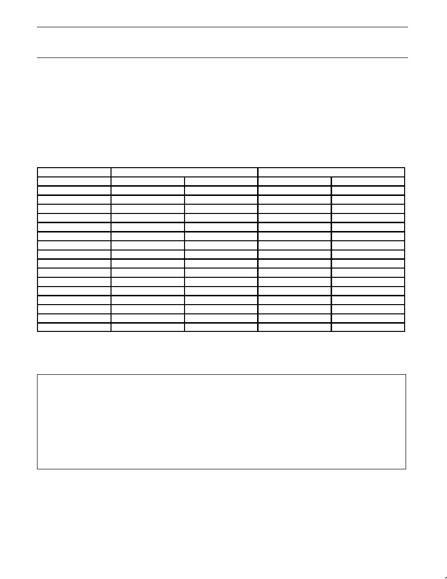
Philips Semiconductors
Product data
SCC68681
Dual asynchronous receiver/transmitter (DUART)
2004 Apr 06
19
Transmitter Disable Note
The sequence of instructions enable transmitter -- load transmit
holding register -- disable transmitter will result in nothing being
sent if the time between the end of loading the transmit holding
register and the disable command is less that 3/16 bit time in the
16
◊
mode or one bit time in the 1
◊
mode. Also, if the transmitter,
while in the enabled state and underrun condition, is immediately
disabled after a single character is loaded to the transmit holding
register, that character will not be sent.
In general, when it is desired to disable the transmitter before the
last character is sent AND the TxEMT bit is set in the status register
(TxEMT is always set if the transmitter has underrun or has just
been enabled), be sure the TxRDY bit is active immediately before
issuing the transmitter disable instruction. TxRDY sets at the end of
the `start bit' time. It is during the start bit that the data in the transmit
holding register is transferred to the transmit shift register.
Non-standard baud rates are available as shown in Table 6 below,
via the BRG Test function.
Table 6.
Baud Rates Extended
Normal BRG
BRG Test
CSR[7:4]
ACR[7] = 0
ACR[7] = 1
ACR[7] = 0
ACR[7] = 1
0000
50
75
4,800
7,200
0001
110
110
880
880
0010
134.5
134.5
1,076
1,076
0011
200
150
19.2 k
14.4 k
0100
300
300
28.8 k
28.8 k
0101
600
600
57.6 k
57.6 k
0110
1,200
1,200
115.2 k
115.2 k
0111
1,050
2,000
1,050
2,000
1000
2,400
2,400
57.6 k
57.6 k
1001
4,800
4,800
4,800
4,800
1010
7,200
1,800
57.6 k
14.4 k
1011
9,600
9,600
9,600
9,600
1100
38.4 k
19.2 k
38.4 k
19.2 k
1101
Timer
Timer
Timer
Timer
1110
I/O2 ≠ 16
◊
I/O2 ≠ 16
◊
I/O2 ≠ 16
◊
I/O2 ≠ 16
◊
1111
I/O2 ≠ 1
◊
I/O2 ≠ 1
◊
I/O2 ≠ 1
◊
I/O2 ≠ 1
◊
NOTE:
Each read on address H`2' will toggle the baud rate test mode. When in the BRG test mode, the baud rates change as shown to the left. This
change affects all receivers and transmitters on the DUART. See
"Extended baud rates for SCN2681, SCN68681, SCC2691, SCC2692,
SCC68681 and SCC2698B" in application notes elsewhere in this publication.
The test mode at address H`A' changes all transmitters and receivers to the 1
◊
mode and connects the output ports to some internal nodes.
Receiver Reset in the Normal Mode (Receiver Enabled)
Reset can be accomplished easily by issuing a receiver software or hardware reset followed by a receiver enable. All receiver data,
status and programming will be preserved and available before reset. The reset will NOT affect the programming.
Receiver Reset in the Wake-Up Mode (MR1[4:3] = 11)
Reset can also be accomplished easily by first exiting the wake-up mode (MR1[4:3] = 00 or 01 or 10), then issuing a receiver software or
hardware reset followed by a wake-up re-entry (MR1[4:3] = 11). All receiver data, status and programming will be preserved and
available before reset. The reset will NOT affect other programming.
The reason for this is the receiver is partially enabled when the parity bits are at `11'. Thus the receiver disable and reset is bypassed by
the partial enabling of the receiver.
SD00097
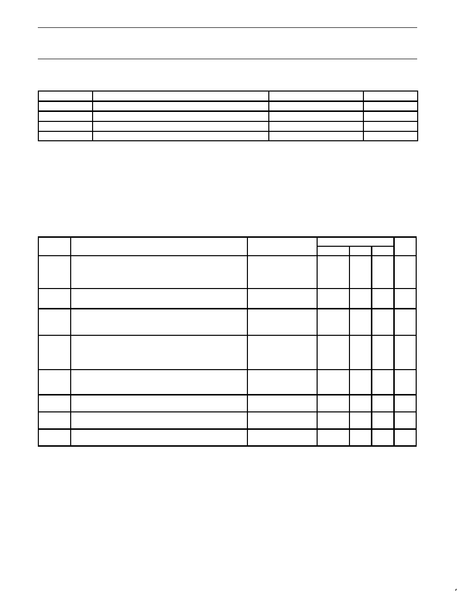
Philips Semiconductors
Product data
SCC68681
Dual asynchronous receiver/transmitter (DUART)
2004 Apr 06
20
ABSOLUTE MAXIMUM RATINGS
1
SYMBOL
PARAMETER
RATING
UNIT
T
amb
Operating ambient temperature range
2
See Note 4
∞
C
T
stg
Storage temperature range
≠65 to +150
∞
C
All voltages with respect to ground
3
≠0.5 to +6.0
V
Maximum pin voltages
V
SS
≠ 0.5 V to V
CC
+ 0.5 V
V
NOTES:
1. Stresses above those listed under Absolute Maximum Ratings may cause permanent damage to the device. This is a stress rating only and
functional operation of the device at these or any other condition above those indicated in the operation section of this specification is not
implied.
2. For operating at elevated temperatures, the device must be derated based on +150
∞
C maximum junction temperature.
3. This product includes circuitry specifically designed for the protection of its internal devices from damaging effects of excessive static
charge. Nonetheless, it is suggested that conventional precautions be taken to avoid applying any voltages larger than the rated maxima.
4. Parameters are valid over specified temperature range. See Ordering information table for applicable operating temperature range and V
CC
supply range.
DC ELECTRICAL CHARACTERISTICS
1, 2, 3
T
amb
= ≠40
∞
C to +85
∞
C;
V
CC
= 5.0 V
±
10%
SYMBOL
PARAMETER
TEST CONDITIONS
LIMITS
UNIT
SYMBOL
PARAMETER
TEST CONDITIONS
Min
Typ
Max
UNIT
V
IL
LOW-level input voltage
≠
≠
0.8
V
V
IH
HIGH-level input voltage (except X1/CLK)
T
amb
0
∞
C
2.0
≠
≠
V
V
IH
HIGH-level input voltage (except X1/CLK)
T
amb
< 0
∞
C
2.5
≠
≠
V
V
IH
HIGH-level input voltage (X1/CLK)
0.8 V
CC
≠
≠
V
V
OL
LOW-level output voltage
I
OL
= 2.4 mA
≠
≠
0.4
V
V
OH
HIGH-level output voltage (except open-drain outputs)
4
I
OH
= ≠400
µ
A
V
CC
≠ 0.5
≠
≠
V
I
IX1
X1/CLK input current
V
IN
= 0 V to V
CC
≠10
≠
+10
µ
A
I
ILX1
X1/CLK input LOW current ≠ operating
V
IN
= 0 V
≠75
≠
0
µ
A
I
IHX1
X1/CLK input HIGH current ≠ operating
V
IN
= V
CC
0
≠
75
µ
A
I
OHX2
X2 output HIGH current ≠ operating
V
OUT
= V
CC
; X1 = 0
0
≠
+75
µ
A
I
OHX2S
X2 output HIGH short circuit current ≠ operating
V
OUT
= 0 V; X1 = 0
≠10
≠
≠1
mA
I
OLX2
X2 output LOW current ≠ operating
V
OUT
= 0 V; X1 = V
CC
≠75
≠
0
µ
A
I
OLX2S
X2 output LOW short circuit current ≠ operating
V
OUT
= V
CC
; X1 = V
CC
1
≠
10
mA
Input leakage current:
I
I
All except input port pins
V
IN
= 0 V to V
CC
≠10
≠
+10
µ
A
Input port pins
V
IN
= 0 V to V
CC
≠20
≠
+10
µ
A
I
OZH
Output off current HIGH, 3-state data bus
V
IN
= V
CC
≠
≠
10
µ
A
I
OZL
Output off current LOW, 3-state data bus
V
IN
= 0 V
≠10
≠
≠
µ
A
I
ODL
Open-drain output LOW current in off-state
V
IN
= 0 V
≠10
≠
≠
µ
A
I
ODH
Open-drain output HIGH current in off-state
V
IN
= V
CC
≠
≠
10
µ
A
I
CC
Power supply current
5
I
CC
Operating mode
CMOS input levels
≠
≠
10
mA
NOTES:
1. Parameters are valid over specified temperature range.
2. All voltage measurements are referenced to ground (GND). For testing, all inputs swing between 0.4 V and 2.4 V with a transition time of
5 ns maximum. For X1/CLK this swing is between 0.4 V and 4.4 V. All time measurements are referenced at input voltages of 0.8 V and
2.0 V and output voltages of 0.8 V and 2.0 V, as appropriate.
3. Typical values are at +25
∞
C, typical supply voltages, and typical processing parameters.
4. Test conditions for outputs: C
L
= 150 pF, except interrupt outputs. Test conditions for interrupt outputs: C
L
= 50 pF, R
L
= 2.7 k
to V
CC
.
5. All outputs are disconnected. Inputs are switching between CMOS levels of V
CC
≠ 0.2 V and V
SS
+ 0.2 V.

Philips Semiconductors
Product data
SCC68681
Dual asynchronous receiver/transmitter (DUART)
2004 Apr 06
21
AC CHARACTERISTICS
1, 2, 3, 4
T
amb
= ≠40
∞
C to +85
∞
C;
V
CC
= 5.0 V
±
10%
SYMBOL
PARAMETER
LIMITS
UNIT
SYMBOL
PARAMETER
Min
Typ
3
Max
UNIT
Reset Timing (See Figure 3)
t
RES
RESETN pulse width
200
ns
Bus Timing
(See Figures 4, 5, 6)
t
AS
A1≠A4 setup time to CSN LOW
10
≠
≠
ns
t
AH
A1≠A4 hold time from CSN LOW
100
≠
≠
ns
t
RWS
RWN setup time to CSN HIGH
0
≠
≠
ns
t
RWH
RWN hold time to CSN HIGH
0
≠
≠
ns
t
CSW
CSN HIGH pulse width
90
≠
≠
ns
t
CSD
5
CSN or IACKN HIGH from DTACKN LOW
20
≠
≠
ns
t
DD
Data valid from CSN or IACKN LOW
≠
≠
175
ns
t
DF
Data bus floating from CSN or IACKN HIGH
7
≠
≠
100
ns
t
DS
Data setup time to CLK HIGH
100
≠
≠
ns
t
DH
Data hold time from CSN HIGH
20
≠
≠
ns
t
DAL
DTACKN LOW from read data valid
0
≠
≠
ns
t
DCR
DTACKN LOW (read cycle) from CLK HIGH
≠
≠
125
ns
t
DCW
DTACKN LOW (write cycle) from CLK HIGH
≠
≠
125
ns
t
DAH
DTACKN HIGH from CSN or IACKN HIGH
≠
≠
100
ns
t
DAT
DTACKN HIGH impedance from CSN or IACKN HIGH
≠
≠
125
ns
t
CSC
6
CSN or IACKN setup time to clock HIGH
90
≠
≠
ns
Port Timing (See Figure 7)
t
PS
Port input setup time to CSN LOW
0
≠
≠
ns
t
PH
Port input hold time from CSN HIGH
0
≠
≠
ns
t
PD
Port output valid from CSN HIGH
≠
≠
400
ns
Interrupt Reset Timing (See Figure 9)
INTRN or OP3≠OP7 when used as interrupts negated from:
Read RHR (RxRDY/FFULL interrupt)
≠
≠
300
ns
Write THR (TxRDY interrupt)
≠
≠
300
ns
t
IR
Reset command (delta break interrupt)
≠
≠
300
ns
IR
Stop C/T command (counter interrupt)
≠
≠
300
ns
Read IPCR (input port change interrupt)
≠
≠
300
ns
Write IMR (clear of interrupt mask bit)
≠
≠
300
ns
Clock Timing (See Figure 8)
t
CLK
X1/CLK HIGH or LOW time
100
≠
≠
ns
f
CLK
8
X1/CLK frequency
0
3.6864
4.0
MHz
t
CTC
CTCLK HIGH or LOW time
100
≠
≠
ns
f
CTC
CTCLK frequency
0
≠
4.0
MHz
t
RX
RxC HIGH or LOW time
220
≠
≠
ns
f
RX
RxC frequency
(16
◊
)
0
≠
2.0
MHz
RX
(1
◊
)
0
≠
1.0
MHz
t
TX
TxC HIGH or LOW time
220
≠
≠
ns
f
TX
TxC frequency
(16
◊
)
0
≠
2.0
MHz
TX
(1
◊
)
0
≠
1.0
MHz
Transmitter Timing (See Figure 10)
t
TXD
TxD output delay from TxC external clock input on IP pin
≠
≠
350
ns
t
TCS
Output delay from TxC LOW at OP pin to TxD data output
≠
≠
150
ns
Receiver Timing (See Figure 11)
t
RXS
RxD data setup time before RxC HIGH at external clock input on IP pin
240
≠
≠
ns
t
RXH
RxD data hold time after RxC HIGH at external clock input on IP pin
200
≠
≠
ns
NOTES:
1. Parameters are valid over specified temperature range. See Ordering information table for applicable operating temperature and V
CC
supply
range.
2. All voltage measurements are referenced to ground (GND). For testing, all inputs except X1/CLK swing between 0.4 V and 2.4 V with
a transition time of 20 ns maximum. For X1/CLK this swing is between 0.4 V and 4.4 V. All time measurements are referenced at input
voltages of 0.8 V and 2.0 V as appropriate.
3. Typical values are at +25
∞
C, typical supply voltages, and typical processing parameters.
4. Test conditions for outputs: C
L
= 150 pF, except interrupt outputs. Test condition for interrupt outputs: C
L
= 50 pF, R
L
= 2.7 k
to V
CC
.
5. This specification will impose maximum 68000 CPU CLK to 6MHz. Higher CPU CLK can be used if repeating bus reads are not performed.
Consecutive write operations to the same command register require at least three edges of the X1 clock between writes.
6. This specification imposes a lower bound on CSN and IACKN LOW, guaranteeing that it will be LOW for at least 1 CLK period. This
requirement is made on CSN only to insure assertion of DTACKN and not to guarantee operation of the part.
7. This spec is made only to insure that DTACKN is asserted with respect to the rising edge of the X1/CLK pin as shown in the timing diagram,
not to guarantee operation of the part. If setup time is violated, DTACKN may be asserted as shown, or may be asserted 1 clock cycle later.
8. Operation to 0 MHz is assured by design. Minimum test frequency is 2.0 MHz.
Philips Semiconductors
Product data
SCC68681
Dual asynchronous receiver/transmitter (DUART)
2004 Apr 06
22
RESETN
t
RES
SD00109
Figure 3. Reset Timing
X1/CLK
A1≠A4
RWN
CSN
D0≠D7
DTACKN
tCSC
tAS
tAH
tRWS
tDF
tDAT
tDAH
tRWH
tCSW
tDD
tCSD
tDAL
tDCR
SD00110
Figure 4. Bus Timing (Read Cycle)
X1/CLK
A1≠A4
RWN
CSN
D0≠D7
DTACKN
tCSC
tAS
tAH
tRWS
tDH
tDAT
tDAH
tRWH
tCSW
tDS
tCSD
tDCW
NOTE:
DACKN requires two rising edges of X1 clock after CEN is low.
SD00111
Figure 5. Bus Timing (Write Cycle)
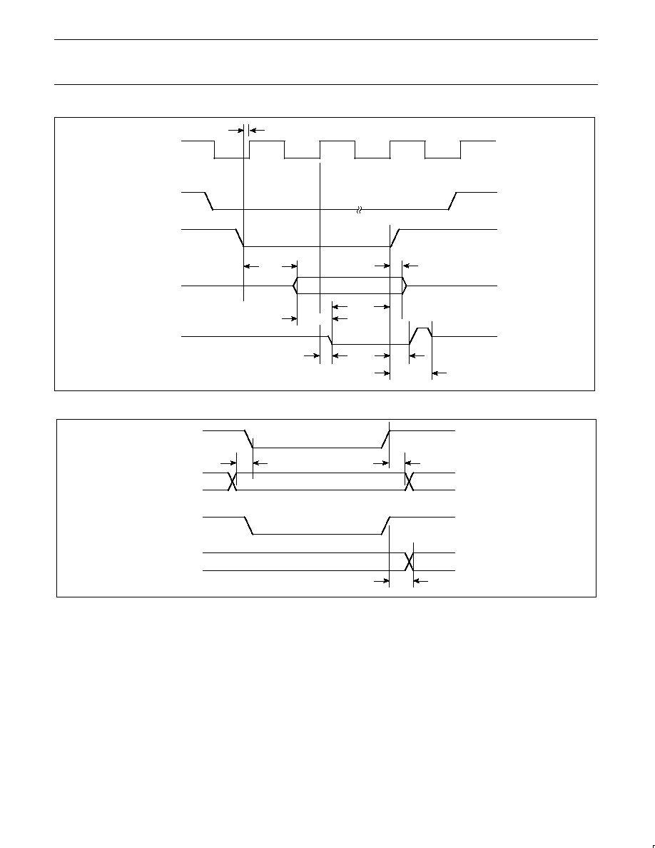
Philips Semiconductors
Product data
SCC68681
Dual asynchronous receiver/transmitter (DUART)
2004 Apr 06
23
X1/CLK
INTRN
IACKN
D0≠D7
DTACKN
tCSC
tDD
tDF
tCSD
tDAL
tDCR
tDAH
tDAT
SD00112
Figure 6. Interrupt Cycle Timing
tPS
tPH
tPD
CSN
IP0≠IP5
CSN
OP0≠OP7
OLD DATA
NEW DATA
SD00113
Figure 7. Port Timing
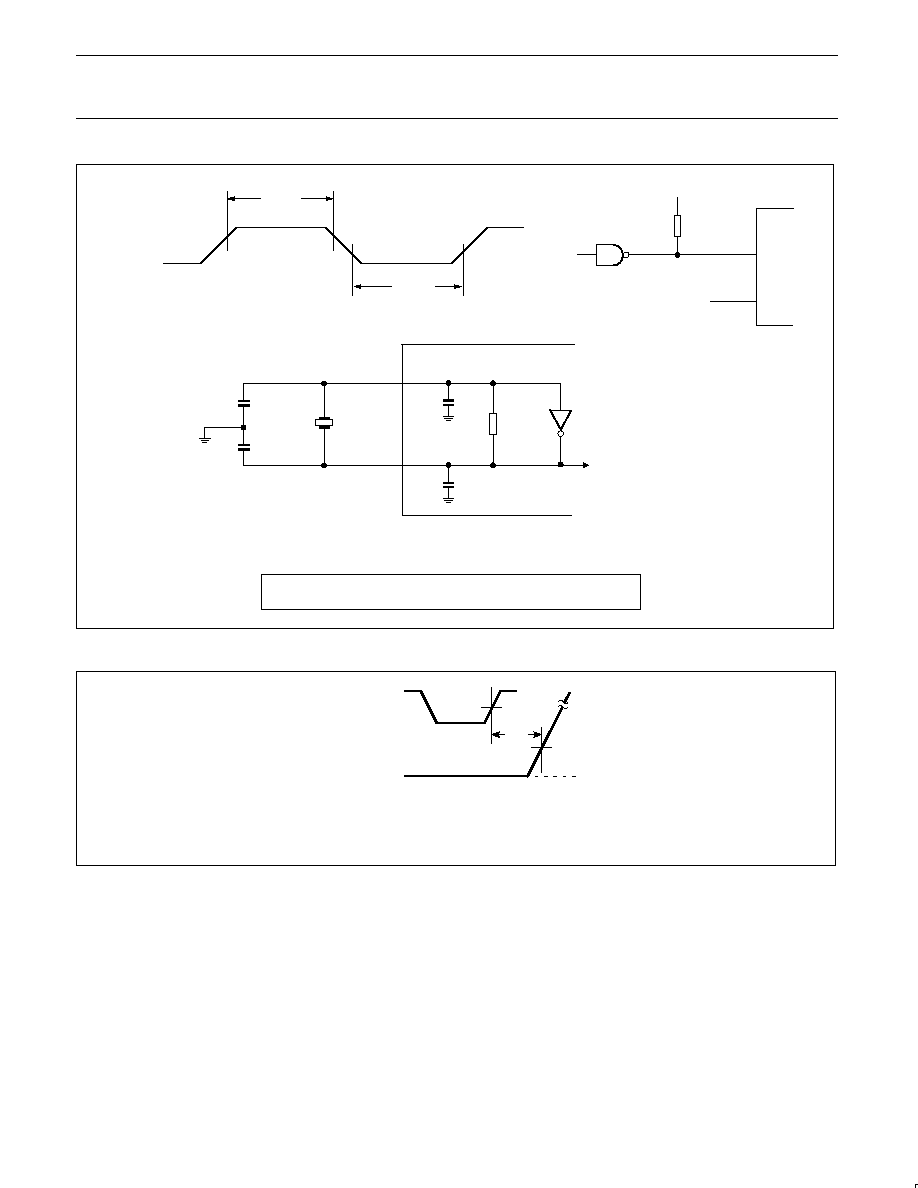
Philips Semiconductors
Product data
SCC68681
Dual asynchronous receiver/transmitter (DUART)
2004 Apr 06
24
X1/CLK
CTCLK
RxC
TxC
t
CLK
t
CTC
t
Rx
t
Tx
t
CLK
t
CTC
t
Rx
t
Tx
+5 V
R1
1 k
X1
X2
C1 = C2 = 24 pF FOR C
L
= 20 pF
X1
X2
3.6864 MHz
3 pF
4 pF
50 TO
150 k
TO INTERNAL CLOCK DRIVERS
SCC68681
NOTE:
C1 AND C2 SHOULD BE BASED ON MANUFACTURER'S SPECIFICATION. PARASITIC CAPACITANCE SHOULD BE
INCLUDED WITH C1 AND C2. R1 IS ONLY REQUIRED IF U1 WILL NOT DRIVE TO X1 INPUT LEVELS
TYPICAL CRYSTAL SPECIFICATION
FREQUENCY:
2 ≠ 4 MHz
LOAD CAPACITANCE (C
L
):
12 ≠ 32 pF
TYPE OF OPERATION:
PARALLEL RESONANT, FUNDAMENTAL MODE
NC
SD00725
RESISTOR REQUIRED
WHEN U1 IS A TTL DEVICE
U1
Figure 8. Clock timing
NOTES:
1. INTRN or OP3 ≠ OP7 when used as interrupt outputs.
2. The test for open drain outputs is intended to guarantee switching of the output transistor. Measurement of this response is referenced from the mid point of the switching signal, V
M
, to
a point 0.5 volts above V
OL
. This point represents noise margin that assures true switching has occurred. Beyond this level, the effects of external circuitry and test environment are
pronounced and can greatly affect the resultant measurement.
VM
VOL
+0.5V
VOL
CSN
(READ OR
WRITE)
INTERRUPT
1
OUTPUT
tIR
SD00116
Figure 9. Interrupt timing
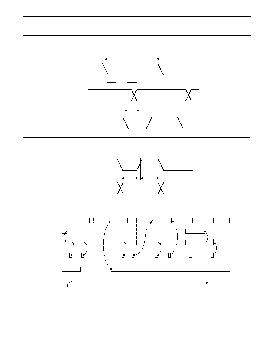
Philips Semiconductors
Product data
SCC68681
Dual asynchronous receiver/transmitter (DUART)
2004 Apr 06
25
tTXD
tTCS
1 BIT TIME
(1 OR 16 CLOCKS)
TxD
TxC
(INPUT)
TxC
(1X OUTPUT)
SD00117
Figure 10. Transmit timing
tRXS
tRXH
RxC
(1X INPUT)
RxD
SD00093
Figure 11. Receive timing
TRANSMITTER
ENABLED
TxD
D1
D2
D3
D4
D6
BREAK
TxRDY
(SR2)
CSN
(WRITE)
D1
D2
D3
D4
D6
START
BREAK
STOP
BREAK
D5 WILL
NOT BE
TRANSMITTED
CTSN
1
(IP0)
RTSN
2
(OP0)
OPR(0) = 1
OPR(0) = 1
NOTES:
1. Timing shown for MR2(4) = 1.
2. Timing shown for MR2(5) = 1.
SD00118
Figure 12. Transmitter timing

Philips Semiconductors
Product data
SCC68681
Dual asynchronous receiver/transmitter (DUART)
2004 Apr 06
26
D1
D2
D3
D4
D5
D6
D7
D8
RxD
D6, D7, D8 WILL BE LOST
RECEIVER
ENABLED
RxRDY
(SR0)
FFULL
(SR1)
RxRDY/
FFULL
(OP4)
2
CSN
(READ)
STATUS DATA
D1
STATUS DATA
D2
STATUS DATA
D3
STATUS DATA
D4
D5 WILL
BE LOST
OVERRUN
(SR4)
RESET BY COMMAND
RTS
1
(OP0)
OPR(0) = 1
NOTES:
1. Timing shown for MR1(7) = 1.
2. Shown for OPCR(4) and MR1(6) = 0.
SD00119
Figure 13. Receive timing
TRANSMITTER
ENABLED
TxD
ADD#1
TxRDY
(SR2)
CSN
(WRITE)
MR1(4+3) = 11
MR1(2) = 1
1
BIT 9
D0
0
BIT 9
ADD#2 1
BIT 9
MASTER STATION
ADD#1 MR1(2) = 0 D0
MR1(2) = 1 ADD#2
RxD
ADD#1 1
BIT 9
D0
0
BIT 9
ADD#2 1
BIT 9
PERIPHERAL STATION
0
BIT 9
0
BIT 9
RECEIVER
ENABLED
RxRDY
(SR0)
CSN
MR1(4:3) = 11
ADD#1
STATUS DATA
D0
STATUS DATA
ADD#2
SD00120
Figure 14. Wake-up mode
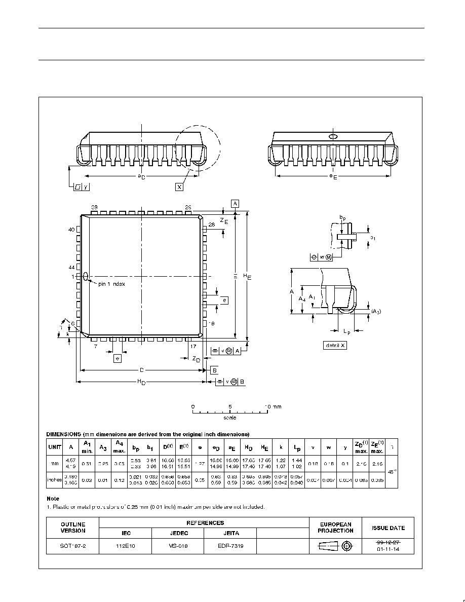
Philips Semiconductors
Product data
SCC68681
Dual asynchronous receiver/transmitter (DUART)
2004 Apr 06
27
PLCC44:
plastic leaded chip carrier; 44 leads
SOT187-2
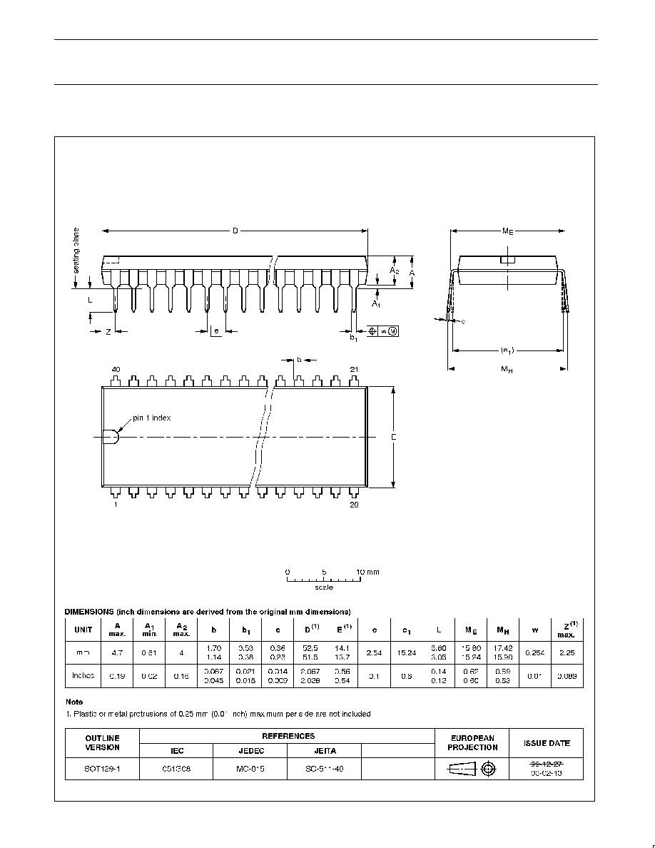
Philips Semiconductors
Product data
SCC68681
Dual asynchronous receiver/transmitter (DUART)
2004 Apr 06
28
DIP40:
plastic dual in-line package; 40 leads (600 mil)
SOT129-1

Philips Semiconductors
Product data
SCC68681
Dual asynchronous receiver/transmitter (DUART)
2004 Apr 06
29
REVISION HISTORY
Rev
Date
Description
_1
20040406
Product data (9397 750 12079). ECN 853-2447 01-A15014 of 15 December 2003.
Definitions
Short-form specification -- The data in a short-form specification is extracted from a full data sheet with the same type number and title. For detailed information see
the relevant data sheet or data handbook.
Limiting values definition -- Limiting values given are in accordance with the Absolute Maximum Rating System (IEC 60134). Stress above one or more of the limiting
values may cause permanent damage to the device. These are stress ratings only and operation of the device at these or at any other conditions above those given
in the Characteristics sections of the specification is not implied. Exposure to limiting values for extended periods may affect device reliability.
Application information -- Applications that are described herein for any of these products are for illustrative purposes only. Philips Semiconductors make no
representation or warranty that such applications will be suitable for the specified use without further testing or modification.
Disclaimers
Life support -- These products are not designed for use in life support appliances, devices, or systems where malfunction of these products can reasonably be
expected to result in personal injury. Philips Semiconductors customers using or selling these products for use in such applications do so at their own risk and agree
to fully indemnify Philips Semiconductors for any damages resulting from such application.
Right to make changes -- Philips Semiconductors reserves the right to make changes in the products--including circuits, standard cells, and/or software--described
or contained herein in order to improve design and/or performance. When the product is in full production (status `Production'), relevant changes will be communicated
via a Customer Product/Process Change Notification (CPCN). Philips Semiconductors assumes no responsibility or liability for the use of any of these products, conveys
no license or title under any patent, copyright, or mask work right to these products, and makes no representations or warranties that these products are free from patent,
copyright, or mask work right infringement, unless otherwise specified.
Contact information
For additional information please visit
http://www.semiconductors.philips.com.
Fax: +31 40 27 24825
For sales offices addresses send e-mail to:
sales.addresses@www.semiconductors.philips.com.
©
Koninklijke Philips Electronics N.V. 2004
All rights reserved. Printed in U.S.A.
Date of release: 04-04
Document order number:
9397 750 12079
Philips
Semiconductors
Data sheet status
[1]
Objective data
Preliminary data
Product data
Product
status
[2] [3]
Development
Qualification
Production
Definitions
This data sheet contains data from the objective specification for product development.
Philips Semiconductors reserves the right to change the specification in any manner without notice.
This data sheet contains data from the preliminary specification. Supplementary data will be published
at a later date. Philips Semiconductors reserves the right to change the specification without notice, in
order to improve the design and supply the best possible product.
This data sheet contains data from the product specification. Philips Semiconductors reserves the
right to make changes at any time in order to improve the design, manufacturing and supply. Relevant
changes will be communicated via a Customer Product/Process Change Notification (CPCN).
Data sheet status
[1] Please consult the most recently issued data sheet before initiating or completing a design.
[2] The product status of the device(s) described in this data sheet may have changed since this data sheet was published. The latest information is available on the Internet at URL
http://www.semiconductors.philips.com.
[3] For data sheets describing multiple type numbers, the highest-level product status determines the data sheet status.
Level
I
II
III