Philips Semiconductors
Product specification
NE/SE5561
Switched-mode power supply control circuit
1
1994 Aug 31
853-0889 13721
DESCRIPTION
The NE5561/SE5561 is a control circuit for use in switched-mode
power supplies. It contains an internal temperature- compensated
supply, PWM, sawtooth oscillator, overcurrent sense latch, and
output stage. The device is intended for low cost SMPS applications
where extensive housekeeping functions are not required.
FEATURES
∑
Micro-miniature (D) package
∑
Pulse-width modulator
∑
Current limiting (cycle-by-cycle)
∑
Sawtooth generator
∑
Stabilized power supply
∑
Double pulse protection
∑
Internal temperature-compensated reference
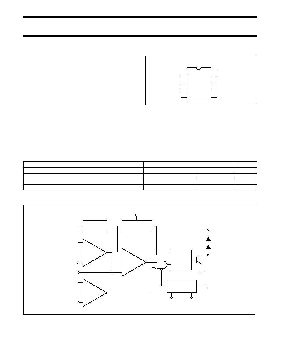
PIN CONFIGURATION
D, FE, N Packages
1
2
3
4
5
6
7
8
VCC
VZ
FEEDBACK
GAIN
GND
OUTPUT
CURRENT SENSE
RT
,
CT
Figure 1. Pin Configuration
APPLICATIONS
∑
Switched-mode power supplies
∑
DC motor controller inverter
∑
DC/DC converter
ORDERING INFORMATION
DESCRIPTION
TEMPERATURE RANGE
ORDER CODE
DWG #
8-Pin Plastic Dual In-Line Package (DIP)
0 to +70
∞
C
NE5561N
SOT97-1
8-Pin Plastic Dual In-Line Package (DIP)
-55 to +125
∞
C
SE5561N
SOT97-1
8-Pin Ceramic Dual In-Line Package (CERDIP)
-55 to +125
∞
C
SE5561FE
0580A
8-Pin Small Outline (SO) Package
0 to +70
∞
C
NE5561D
SOT96-1
BLOCK DIAGRAM
REF
VOLTAGE
SAWTOOTH
GENERATOR
PWM
ERROR
AMP
FEEDBACK
GAIN
0.5V
CURRENT
SENSE
LATCH
S
R
GND
8.2V
OUTPUT
STABILIZED
SUPPLY
1
8
2
+
7
5
3
4
6
≠
+
≠
VCC
VZ
RT
,
CT
VCC
SL00385
Figure 2. Block Diagram
Philips Semiconductors
Product specification
NE/SE5561
Switched-mode power supply control circuit
1994 Aug 31
2
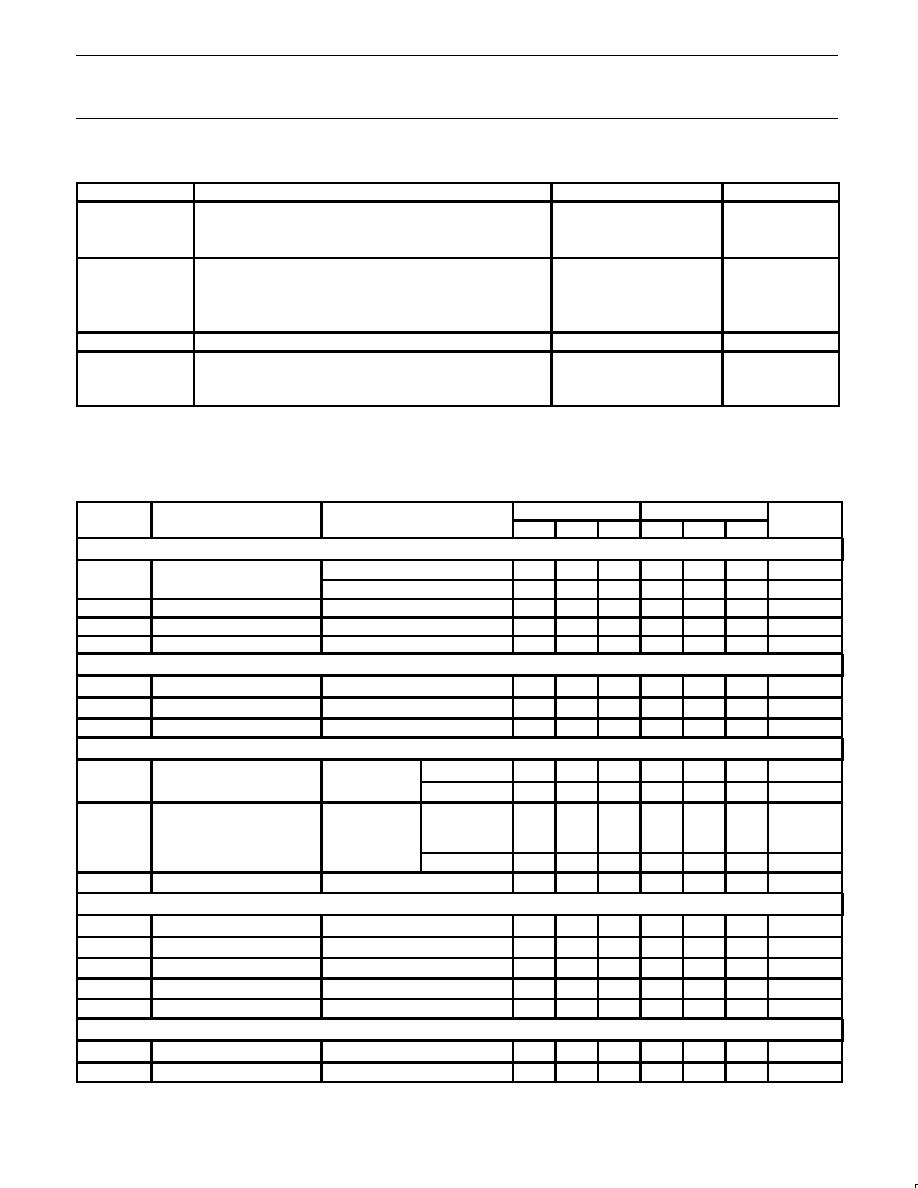
ABSOLUTE MAXIMUM RATINGS
SYMBOL
PARAMETER
RATING
UNIT
V
CC
Supply
1
Voltage-forced mode
+18
V
Current-fed mode
30
mA
Output transistor (at 20-30V max)
I
OUT
Output current
40
mA
V
OUT
Output voltage
V
CC
+1.4V
V
Output duty cycle
98
%
P
D
Maximum total power dissipation
0.75
W
T
A
Operating temperature range
SE5561
-55 to +125
∞
C
NE5561
0 to 70
∞
C
NOTES:
1. See Voltage-Current-fed supply characteristic curve.
DC ELECTRICAL CHARACTERISTICS
V
CC
=12V, T
A
=25
∞
C, unless otherwise specified.
SYMBOL
PARAMETER
TEST CONDITIONS
SE5561
NE5561
UNIT
SYMBOL
PARAMETER
TEST CONDITIONS
Min
Typ
Max
Min
Typ
Max
UNIT
Reference section
V
REF
Internal ref voltage
T
A
=25
∞
C
3.69
3.75
3.84
3.57
3.75
3.96
V
Over temperature
3.65
3.88
3.55
3.98
V
V
Z
Internal zener ref
*I
L
=7mA
7.8
8.2
8.8
7.8
8.2
8.8
V
Temp. coefficient of V
REF
±
100
±
100
ppm/
∞
C
Temp. coefficient of V
Z
±
200
±
200
ppm/
∞
C
Oscillator section
Frequency range
Over temperature
50
100k
50
100k
Hz
Initial accuracy
R
T
and C
T
constant
5
5
%
Duty cycle range
f
O
=20kHz
0
98
0
98
%
Current limiting
I
IN
Input current
Pin 6=250mV
T
A
=25
∞
C
-2
-10
-2
-10
µ
A
Over temp.
-20
-20
µ
A
Single pulse inhibit delay
Inhibit delay
time for 20%
overdrive at
I
OUT
=20mA
0.88
1.10
0.88
1.10
µ
s
I
OUT
=40mA
0.7
0.8
0.7
0.8
µ
s
Current limit trip level
.400
.500
.600
.400
.500
.600
V
Error amplifier
Open-loop gain
60
60
dB
Feedback resistor
10k
10k
BW
Small-signal bandwidth
3
3
MHz
V
OH
Output voltage swing
6.2
6.2
V
V
OL
Output voltage swing
0.7
0.7
V
Output stage
I
OUT
Output current
Over temperature
20
20
mA
V
CE
Sat
I
C
=20mA, Over temp.
0.4
0.4
V
Philips Semiconductors
Product specification
NE/SE5561
Switched-mode power supply control circuit
1994 Aug 31
4
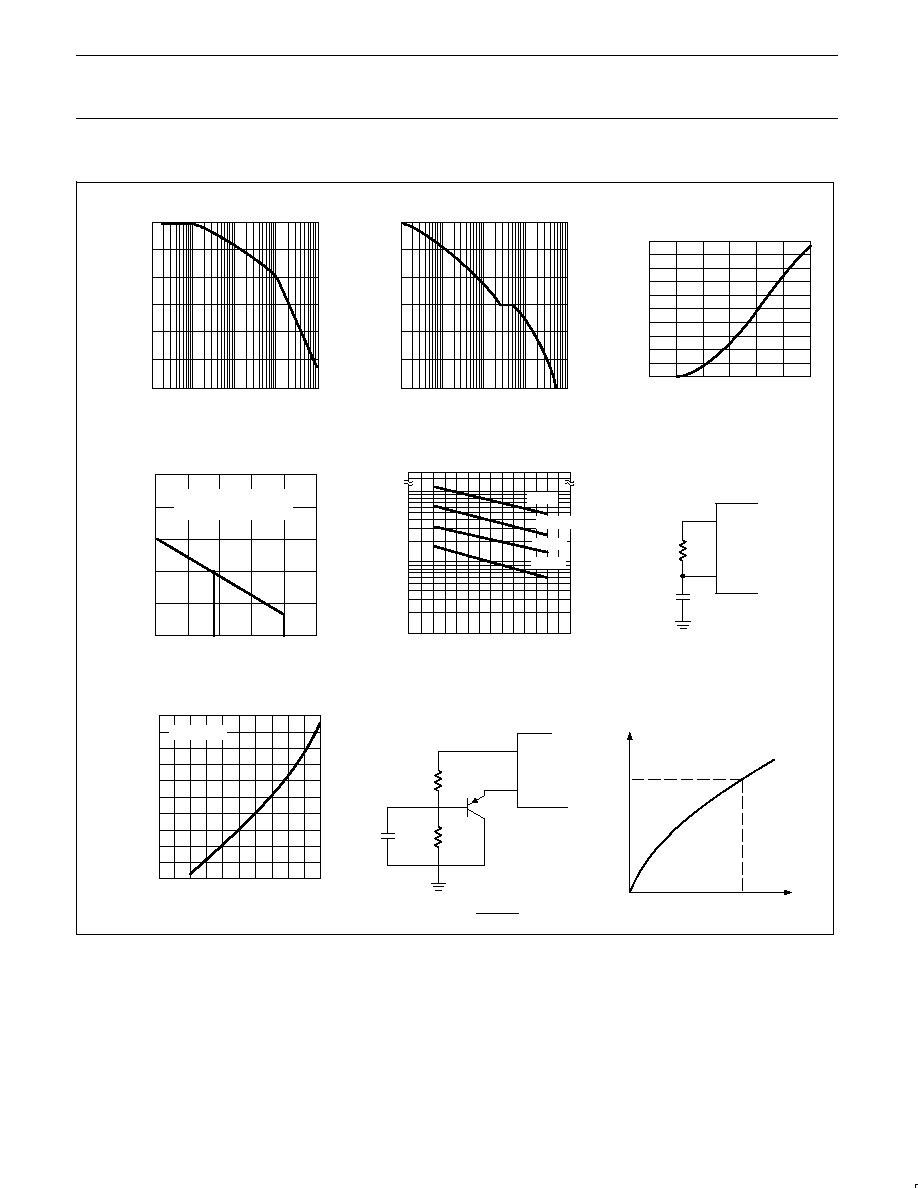
TYPICAL PERFORMANCE CHARACTERISTICS
GAIN (dB)
C (nF)
d
max is a function of f
R2
R1
)
R2
V
Z
)
V
BEQ1
Error Amplifier
Open-Loop Gain
Error Amplifier
Open-Loop Phase
Transfer Curve of Pulse-Width
Modulator Duty Cycle vs Input Voltage
Power Derating Curve
Typical Frequency Plot vs R
T
and C
T
Maximum Duty Cycle vs
Base Voltage on Q1
Start-Up Circuit
Slow-Start Voltage
100
90
80
70
60
50
40
30
20
10
0
0
1
2
3
4
5
V1
MAXIMUM DUTY
CYCLE (%)
MAX (%)
V4
t
t = R'C
2
4
Q1
R2
V1
C
R1
NE5561
VZ
2
5
NE5561
RT
CT
1.25
1.00
0.75
0.50
0.25
0
25
50
70
100
125
150
T
OT
AL
PWR DISSIP
A
TION (W
A
TTS)
NE
SE
AMBIENT TEMPERATURE (
∞
C)
PT = VCC ICC + (VCC ≠ VZ) IZ
+ [V7 I7 x DUTY CYCLE]
100
90
80
70
60
50
40
30
20
10
0
0
1
2
3
4
5
6
V4
(%)
1000
100
50
30
20
10
5
3
2
1
2
2.5
3
3.5
4
4.5
f (kHz)
R=10k
R=20k
R=40k
R=5k
60
50
40
30
20
10
0
1k
10k
100k
1M
10M
FREQUENCY (Hz)
PHASE
ANGLE (DEG)
0
1k
10k
100k
1M
10M
FREQUENCY (Hz)
≠30
≠60
≠90
≠120
≠150
≠180
SL00386
Figure 3. Typical Performance Characteristics
Philips Semiconductors
Product specification
NE/SE5561
Switched-mode power supply control circuit
1994 Aug 31
5
R
VCC
+
V
S
*
V
CC
(10 20mA)
NOTE:
See DC Electrical Characteristics for Current Fed VCC Range.
NE5561 Voltage-Current-Fed
Supply Characteristics
Current-Fed Dropping Resistor
VS
RVCC
VCC
GND
1
8
mA
20
10
0
0
10
20
30
V
SL00387
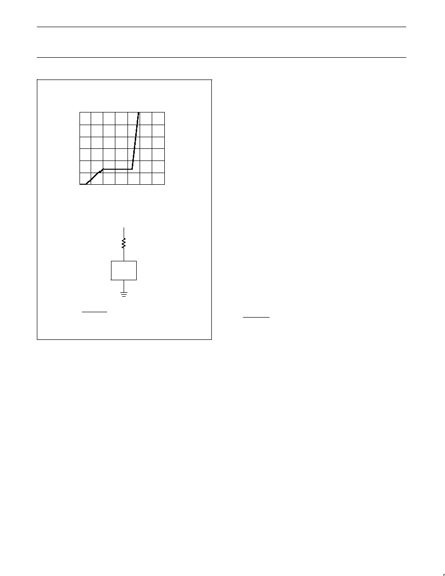
Figure 4. NE5561 Voltage-Current-Fed Supply Characteristics
NE5561 START-UP
The start-up, or initial turn-on, of this device requires some degree of
external protective duty cycle limiting to prevent the duty cycle from
initially going to the extreme maximum (
>90%). Either overcurrent
limit or slow-start circuitry must be employed to limit duty cycle to a
safe value during start-up. Both may be used, if desired.
To implement slow-start, the start-up circuit can be used. The divider
R1 and R2 sets a voltage, buffered by Q1, such that the output of
the error amplifier is clamped to a maximum output voltage, thereby
limiting the maximum duty cycle. The addition of capacitor C will
cause this voltage to ramp-up slowly when power is applied, causing
the duty cycle to ramp-up simultaneously.
Overcurrent limit may be used also. To limit duty cycle in this mode,
the switch current is monitored at Pin 6 and the output of the 5561 is
disabled on a cycle-by-cycle basis when current reaches the
programmed limit. With current limit control of slow-start, the duty
cycle is limited to that value, just allowing maximum switch current
to flow. (Approximately 0.50V measured at Pin 6.)
APPLICATIONS
5V, 0.5A Buck Regulator Operates from 15V
The converter design shows how simple it is to derive a TTL supply
from a system supply of 15V (see Figure 1). The NE5561 drives a
2N4920 PNP transistor directly to provide switching current to the
inductor.
Overall line regulation is excellent and covers a range of 12V to 18V
with minimal change (<10mV) in the output operating at full load.
As with all NE5561 circuits, the auxiliary slow start and
MAX
circuit
is required, as evidenced by Q1. The
MAX
limit may be calculated
by using the relationship:
R2
R1
)
R2
(8.2V)
+
V
d
MAX
The maximum duty cycle is then determined from the pulse-width
modulator transfer graph, with R1 and R2 being defined from the
desired conditions.