Document Outline
- 1 Contents
- 2 Definitions
- 2.1 Life Support Applications
- 2.2 Abbreviations
- 3 Scope
- 4 Ordering Information
- 5 Functional Description
- 5.1 Basic Features
- 5.2 Block Diagram of the IC
- 5.3 Memory Organisation
- 6 Mechanical Die Specifications
- 7 Mechanical Wafer Specifications
- 7.1 Wafer Status
- 7.2 Backside Treatment
- 8 Documentation
- 8.1 Delivery Documentation
- 8.2 Fail-Die Identification
- 9 Quality Assurance
- 9.1 Electrical Acceptance Test
- 9.2 Visual Inspection
- 10 Packing
- 10.1 Storage Recommendations
- 10.2 Possible Forms of Delivery
- 11 Handling Recommendations
- 12 Coil Specification
- 13 Electrical Specifications
- 14 Hints for Label IC Encapsulation
- 14.1 Protection against Visible Light
- 14.2 Protection against UV Light
- 14.3 Resistance to X-Rays
- 15 Inlet/Label Characterisation and Test
- 15.1 Characterisation of the Inlet/Label
- 15.2 Final Test of the Inlet/Label
- 16 Appendix A: Die Plan
- 17 Appendix B: Cluster Plan
- 18 Appendix C: Cluster Map
- 19 Appendix D: Wafer Map
INTEGRATED CIRCUITS
SL1 ICS31 01
I∑CODE
1 Label IC (97pF)
Chip Specification
Product Specification
Revision 1.2
Public
July 2000
Philips
Semiconductors

Product Specification
SL1 ICS31 01
Rev. 1.2
July 2000
Page 2 of 22
Public
1 Contents
1
CONTENTS
2
2
DEFINITIONS
4
2.1
Life Support Applications .................................................................................................... 4
2.2
Abbreviations ........................................................................................................................ 4
3
SCOPE
5
4
ORDERING INFORMATION
5
5
FUNCTIONAL DESCRIPTION
6
5.1
Basic Features ....................................................................................................................... 6
5.2
Block Diagram of the IC....................................................................................................... 6
5.3
Memory Organisation........................................................................................................... 7
5.3.1
Serial Number................................................................................................................... 7
5.3.2
Write Access Conditions .................................................................................................. 7
5.3.3
Special Functions (EAS/QUIET)..................................................................................... 8
5.3.4
Family Code and Application Identifier........................................................................... 8
5.3.5
Configuration of delivered ICs......................................................................................... 8
6
MECHANICAL DIE SPECIFICATIONS
9
7
MECHANICAL WAFER SPECIFICATIONS
10
7.1
Wafer Status ........................................................................................................................ 10
7.2
Backside Treatment ............................................................................................................ 10
8
DOCUMENTATION
11
8.1
Delivery Documentation..................................................................................................... 11
8.2
Fail-Die Identification......................................................................................................... 11
8.2.1
Ink Dot Specification...................................................................................................... 11
8.2.2
Wafer Mapping............................................................................................................... 11
9
QUALITY ASSURANCE
12
9.1
Electrical Acceptance Test................................................................................................. 12
9.2
Visual Inspection................................................................................................................. 12
9.2.1
After Wafer Final Test.................................................................................................... 12
9.2.2
After Sawing (Film Frame Carrier)................................................................................ 12
10
PACKING
13
10.1 Storage Recommendations ................................................................................................. 13
10.2 Possible Forms of Delivery ................................................................................................. 13
10.2.1 Packing of Unsawn Wafers............................................................................................ 13
10.2.2 Packing of Sawn Wafers ................................................................................................ 13

Product Specification
SL1 ICS31 01
Rev. 1.2
July 2000
Page 3 of 22
Public
11
HANDLING RECOMMENDATIONS
14
11.1 Sawing .................................................................................................................................. 14
11.2 Die Attach............................................................................................................................. 14
11.3 Wire Bonding....................................................................................................................... 14
12
COIL SPECIFICATION
14
13
ELECTRICAL SPECIFICATIONS
15
14
HINTS FOR LABEL IC ENCAPSULATION
16
14.1 Protection against Visible Light......................................................................................... 16
14.2 Protection against UV Light............................................................................................... 16
14.3 Resistance to X-Rays .......................................................................................................... 16
15
INLET/LABEL CHARACTERISATION AND TEST
17
15.1 Characterisation of the Inlet/Label ................................................................................... 17
15.2 Final Test of the Inlet/Label............................................................................................... 17
16
APPENDIX A: DIE PLAN
18
17
APPENDIX B: CLUSTER PLAN
19
18
APPENDIX C: CLUSTER MAP
20
19
APPENDIX D: WAFER MAP
21
Product Specification
SL1 ICS31 01
Rev. 1.2
July 2000
Page 4 of 22
Public
2 Definitions
Data sheet status
Objective specification
This data sheet contains target or goal specifications for product development.
Preliminary specification
This data sheet contains preliminary data; supplementary data may be published later.
Product specification
This data sheet contains final product specifications.
Limiting values
Limiting values given are in accordance with the Absolute Maximum Rating System (IEC 134). Stress above one
or more of the limiting values may cause permanent damage to the device. These are stress ratings only and
operation of the device at these or at any other conditions above those given in the Characteristics section of the
specification is not implied. Exposure to limiting values for extended periods may affect device reliability.
Application information
Where application information is given, it is advisory and does not form part of the specification.
2.1 Life Support Applications
These products are not designed for use in life support appliances, devices, or systems where
malfunction of these products can reasonably be expected to result in personal injury. Philips
customers using or selling these products for use in such applications do so on their own risk and
agree to fully indemnify Philips for any damages resulting from such improper use or sale.
2.2 Abbreviations
ASCII
American Standard Code for Information Interchange
CRC
Cyclic Redundancy Check
EAN
European Article Number
EAS
Electronic Article Surveillance
EEPROM
Electrically Erasable and Programmable Read Only Memory
EMI
Electromagnetic Interference
ETSI
European Telecommunications Standards Institute
FCC
Federal Communications Commission
FFC
Film Frame Carrier
Hex
Value in hexadecimal notation
IC
Integrated Circuit
ISM
Industrial, Scientific, Medical
LSB
Least Significant Bit or Byte
MSB
Most Significant Bit or Byte
MTBF
Mean Time Between Failure
PCB
Printed Circuit Board
PCM
Process Control Module
RF
Radio Frequency
rms
Root Mean Square
SNR
Serial Number
UV
Ultraviolet
Product Specification
SL1 ICS31 01
Rev. 1.2
July 2000
Page 5 of 22
Public
3 Scope
This specification describes the electrical, physical and dimensional properties of unsawn and sawn
wafers on FFC of I∑CODE1 Label ICs (C
res
= 97 pF) on a Philips 6C15 IDFW process and is the
base for delivery of tested I∑CODE1 Label ICs.
General recommendations are given for storage, handling and processing of wafers as well as
assembly of labels.
Reference documents:
MIL-STD 883D Method 3023
MIL-STD 883D Method 3015
SNW-FQ-627
PICTOH-QS007
General Specification for 6" Wafer
General Quality Specification
I∑CODE Label IC, Coil Design Guide
This product specification is valid for mask revision: VCOL1V0 NK: O MB: B
4 Ordering Information
Following ordering options are available:
Type Name
Description
Ordering Code
SL1 ICS31 01W/N5D Sawn wafer on foil (FFC), 150 µm, inked and mapped
9352 670 53005
SL1 ICS31 01U/N5D
Unsawn wafer, 150 µm, inked and mapped
9352 670 50025
SL1 ICS31 01U/L6D
Unsawn wafer, 525 µm, mapped (not inked)
9352 670 59025
Product Specification
SL1 ICS31 01
Rev. 1.2
July 2000
Page 6 of 22
Public
5 Functional Description
5.1 Basic Features
The I∑CODE1 Label IC is a dedicated chip for intelligent label applications like logistics and retail
(including EAS) as well as baggage and parcel identification in airline business and mail services.
The I∑CODE system offers the possibility of operating labels simultaneously in the field of the
reader antenna (Anticollision). It is designed for long range applications.
Whenever connected to a very simple and cheap type of antenna (as a result of the 13.56 MHz
carrier frequency) made out of a few windings printed, wound, etched or punched coil the I∑CODE1
Label IC can be operated without line of sight up to a distance of 1.5 m (gate width).
5.2 Block Diagram of the IC
The label requires no internal power supply. Its contactless interface generates the power supply
and the system clock via the resonant circuitry by inductive coupling to the reader. The interface
also demodulates data that is transmitted from the reader to the I∑CODE Label and modulates the
electromagnetic field for data transmission from the I∑CODE Label to the reader.
Data is stored in a non-volatile memory (EEPROM). The EEPROM has a memory capacity of 512
bit and is organised in 16 blocks consisting of 4 bytes each (1 block = 32 bits). The higher 12 blocks
contain user data and the lowest 4 blocks contain the serial number, the write access conditions and
some configuration bits.
Product Specification
SL1 ICS31 01
Rev. 1.2
July 2000
Page 7 of 22
Public
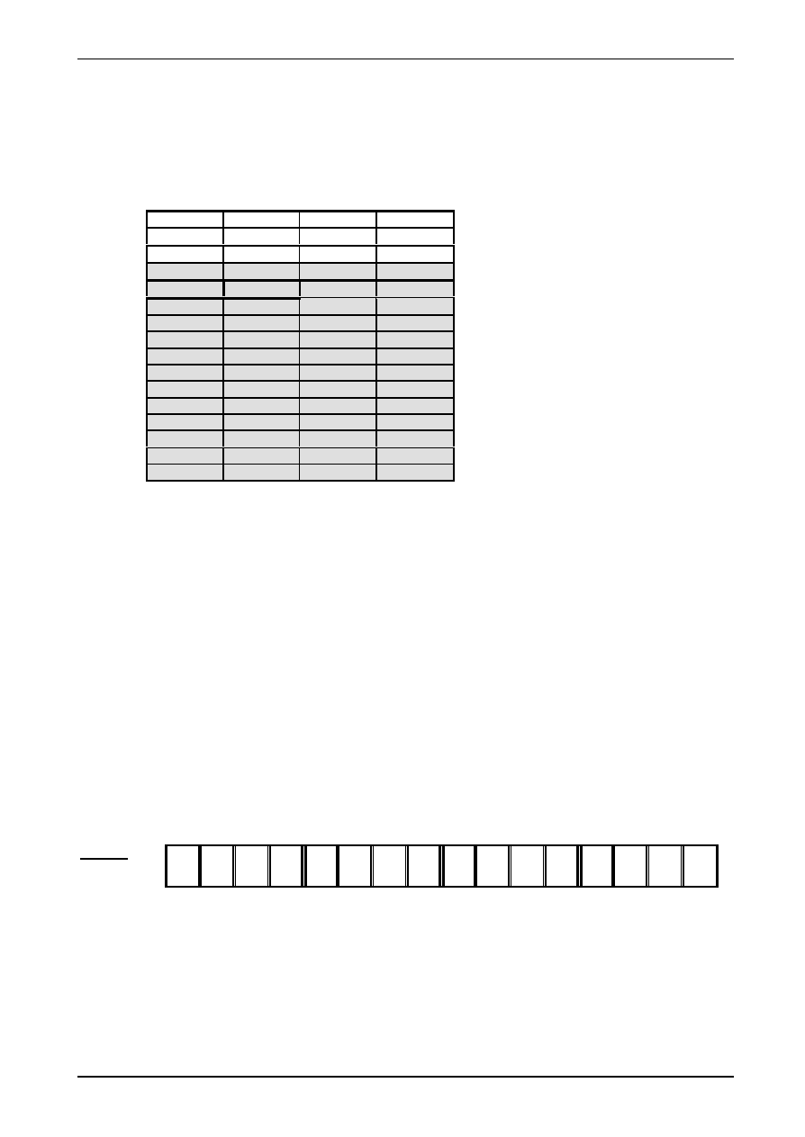
5.3 Memory Organisation
The 512 bit EEPROM memory is divided into 16 blocks. A block is the smallest access unit. Each
block consists of 4 bytes (1 block = 32 bits). Bit 0 in each byte represents the least significant bit
(LSB) and bit 7 the most significant bit (MSB), respectively.
Byte 0
Byte 1
Byte 2
Byte 3
Block 0
SNR0
SNR1
SNR2
SNR3
Serial Number (lower bytes)
Block 1
SNR4
SNR5
SNR6
SNR7
Serial Number (higher bytes)
Block 2
F0
FF
FF
FF
Write Access Conditions
Block 3
x
x
x
x
Special Functions (EAS/QUIET)
Block 4
x
x
x
x
Family Code/Application Identifier/User Data
Block 5
x
x
x
x
User Data
Block 6
x
x
x
x
:
Block 7
x
x
x
x
:
Block 8
x
x
x
x
:
Block 9
x
x
x
x
:
Block 10
x
x
x
x
:
Block 11
x
x
x
x
:
Block 12
x
x
x
x
:
Block 13
x
x
x
x
:
Block 14
x
x
x
x
:
Block 15
x
x
x
x
User Data
The values (in hexadecimal notation) shown in the table above are stored in the EEPROM after the
wafer production process. The content of blocks marked with `
x
' in the table is not defined at
delivery.
5.3.1 Serial Number
The unique 64 bit serial number is stored in blocks 0 and 1 and is programmed during the
production process. SNR0 in the table represents the least significant byte and SNR7 the most
significant byte, respectively.
5.3.2 Write Access Conditions
The Write Access Condition bits in block 2 determine the write access conditions for each of the
16 blocks. These bits can be set only to 0 (and never be changed to 1), i.e. already write protected
blocks can never be written to from this moment on. This is also true for block 2. If this block is set
into write protected state by clearing of bits 4 and 5 at byte 0, no further changes in write access
conditions are possible.
Byte 0
Byte 1
Byte 2
Byte 3
‚
MSB LSB
‚
‚
MSB LSB
‚
‚
MSB LSB
‚
‚
MSB LSB
‚
Block 2:
Write Access
Conditions
|
1|1
|
|
1|1
|
|
0
|
0
|
|
0
|
0
|
|
1|1
|
|
1|1
|
|
1|1
|
|
1|1
|
|
1|1
|
|
1|1
|
|
1|1
|
|
1|1
|
|
1|1
|
|
1|1
|
|
1|1
|
|
1|1
|
for Block
ý
3
2
1
0
7
6
5
4
11
10
9
8
15
14
13
12
Special
Funct.
Write
Access
Serial
Number
User
Data
..... ..... ..... ..... ..... ..... ..... ..... ..... .....
User
Data
The ones in the 16 pairs of bits have to be cleared together if the corresponding block is wanted to
be write protected forever (
1|1
ý write access enabled,
0|0
ý write access disabled). Writing of bit
pairs
1|0
or
0|1
to block 2 is not allowed!
It is extremely important to be particularly careful when clearing the Write Access bits in
block 2, as you can lose write access to all of the blocks on the label in case of a mistake.
Of course you can use this feature to put the label into a hardware write protected state!
Product Specification
SL1 ICS31 01
Rev. 1.2
July 2000
Page 8 of 22
Public
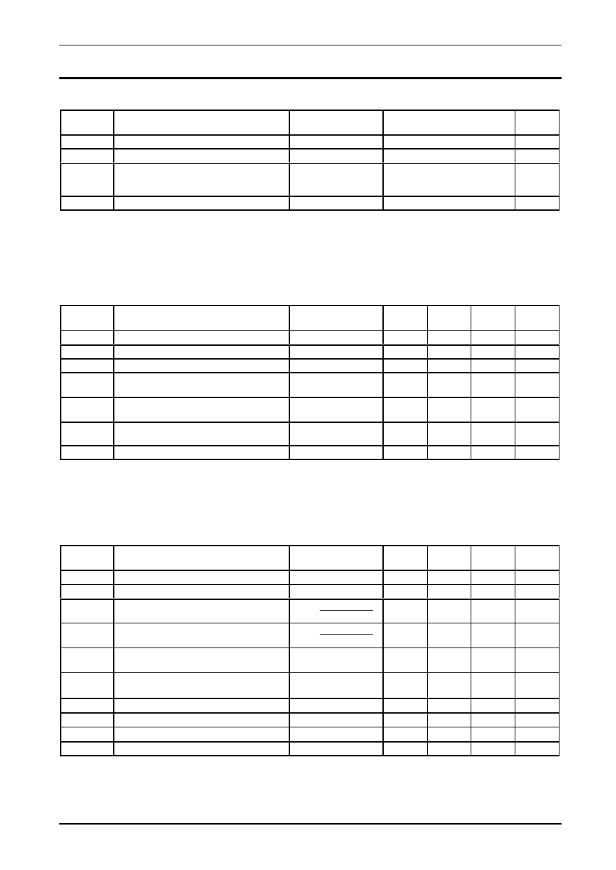
5.3.3 Special Functions (EAS/QUIET)
The Special Functions block holds the two EAS bits (Electronic Article Surveillance mode active
ý the label answers at an EAS command) as well as the two QUIET bits (QUIET mode enabled ý
the label is permanently disabled but can be activated again with the `Reset QUIET bit' command).
The state of QUIET mode does not influence the functionality of the EAS command.
The remaining 28 bits (greyed `
x
' in the following figure) are reserved for future use.
Byte 0
Byte 1
Byte 2
Byte 3
‚
MSB LSB
‚
Block 3:
Special
Functions
|
x|x
|
|
x|x
|
|
q|q
|
|
e|e
|
|
x|x
|
|
x|x
|
|
x|x
|
|
x|x
|
|
x|x
|
|
x|x
|
|
x|x
|
|
x|x
|
|
x|x
|
|
x|x
|
|
x|x
|
|
x|x
|
Quiet
EAS
Quiet:
q|q
=
1|1
ý QUIET mode enabled
q|q
=
0|0
ý QUIET mode disabled
EAS:
e|e
=
1|1
ý EAS mode enabled
e|e
=
0|0
ý EAS mode disabled
Writing of bit pairs
1|0
or
0|1
to block 3 is not allowed!
Changing of the Write Access Control or Configuration must be done in secure environment
(by reading the current value of the block and masking in the new values for bit positions that
may be changed). The label must not be moved out of the communication field of the antenna
during writing! We recommend to put the label close to the antenna and not to remove it
during operation.
5.3.4 Family Code and Application Identifier
The I∑CODE system offers the feature to use (independently) Family Codes and/or Application
Identifiers with some reader commands (this allows for example the creation of `label families').
These two 8-bit values are located at the beginning of User Data (block 4) as shown in the
following figure and are only evaluated if the corresponding bytes at the reader commands are
unequal to zero.
Only if both corresponding parameter bytes at the reader commands Anticollision/Select, EAS and
Unselected Read, respectively, are set to zero, block 4 can be used for user data without restriction.
Byte 0
Byte 1
Byte 2
Byte 3
‚
MSB LSB
‚ ‚
MSB LSB
‚
Block 4:
Family Code,
Application ID
|
x
|
x
|
|
x
|
x
|
|
x
|
x
|
|
x
|
x
|
|
x
|
x
|
|
x
|
x
|
|
x
|
x
|
|
x
|
x
|
|
x
|
x
|
|
x
|
x
|
|
x
|
x
|
|
x
|
x
|
|
x
|
x
|
|
x
|
x
|
|
x
|
x
|
|
x
|
x
|
Family Code
Application ID
The greyed bytes are for customer usage as well as the remaining blocks (5 to 15) are.
5.3.5 Configuration of delivered ICs
I∑CODE1 Label ICs are delivered with the following configuration by Philips:
∑
Serial number is unique and read only
∑
Write Access Conditions allow to change all blocks (with the exception of both serial number blocks)
∑
Status of EAS mode is not defined
∑
Status of QUIET mode is not defined
∑
Family Code and Application Identifier are not defined
∑
User Data memory is not defined
As the status of QUIET mode is not defined at delivery, the first command to be executed on
the I∑CODE1 Label IC should be the Reset QUIET Bit command!

Product Specification
SL1 ICS31 01
Rev. 1.2
July 2000
Page 9 of 22
Public
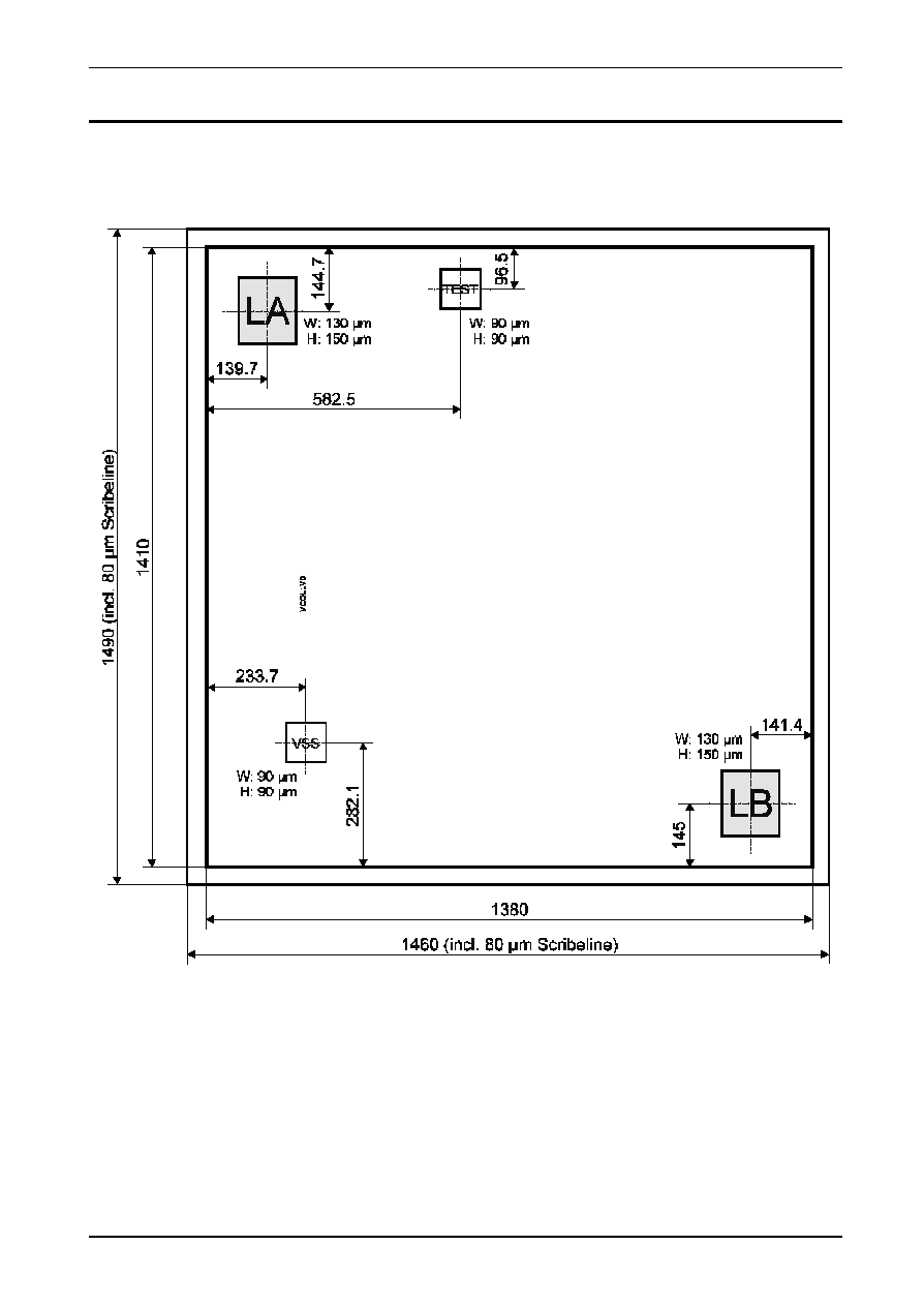
6 Mechanical Die Specifications
Designation:
VCOL1V0
visible on each die
location see attached die plan
Bond pad location:
see attached die plan
Bond pad size:
LA, LB
130 µm x 150 µm
Test pad size:
TEST, VSS
90 µm x 90 µm (the test pads are electrically neutral
at sawn wafers)
Bond pad metallisation material:
AlSiCu
Metallisation thickness:
1.4 µm
Die dimensions
(incl. 80 µm scribe line)
:
1460 µm x 1490 µm
Die dimensions
(excl. scribe line)
:
1380 µm x 1410 µm
Tolerances for sawn dies:
±
25 µm
Pin identification:
see attached die plan
Passivation attributes:
The passivation is a protection of active areas against dust (particles) and humidity and general
contamination (whole surface of the chip except for the bond pads).
Top side passivation material:
Oxynitride
Passivation thickness:
1.6 µm
Due to the glass-like physical properties careful handling and processing is required.

Product Specification
SL1 ICS31 01
Rev. 1.2
July 2000
Page 10 of 22
Public
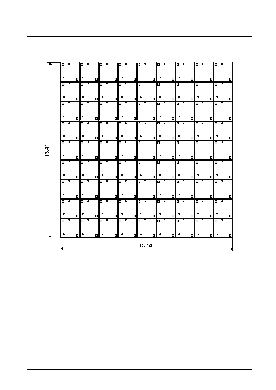
7 Mechanical Wafer Specifications
For further information as described in the following chapters please refer to the following
Philips documents:
∑
Dicing Guidelines for Thin Wafers (< 200 µm)
∑
General Specification for 6" Wafer
In case of doubt or inconsistency with the following chapters the above mentioned specifications
are applicable.
Designation:
each wafer is laser scribed with batch and wafer number
Wafer diameter:
150 mm (6")
±
0.3 mm
Die separation lane width:
80 µm (Scribe line)
Electrical connection of substrate:
VSS
Geometrically complete dies per wafer: approx. 7400
Orientation of dies relat. to wafer flat:
see attached cluster map
Position of test structures:
see attached cluster map
Wafer layout:
see attached cluster map
Batch size:
24 wafers
Process:
6C15 IDFW
7.1 Wafer Status
∑
Tested, unsawn
∑
Tested, sawn on FFC
Minimum yield per lot:
30 %
7.2 Backside Treatment
Wafers can be delivered with a thickness of 525 µm (untreated) or with 150
µ
m
±
15 µm (approx.
6 mil) and have a ground and etched backside.

Product Specification
SL1 ICS31 01
Rev. 1.2
July 2000
Page 11 of 22
Public
8 Documentation
8.1 Delivery Documentation
Each wafer container and each larger shipment container is individually marked with the
identification information as follows:
∑
Diffusion Batch number (wafer lot number)
∑
Part designation (type) with revision number
∑
Ordering code (see chapter 4)
∑
Date code of lot acceptation
∑
Good die quantity
The print out of the final test results is attached to the packing and contains the good die quantity
related to every wafer number.
8.2 Fail-Die Identification
Every die is electrically tested according to data sheet. Identification of chips, which do not confirm
with the electrical parameters of the data sheet is done by inking and/or wafer mapping (all dies at
wafer periphery are identified by `FAIL').
8.2.1 Ink Dot Specification
Diameter:
min. 0.4 mm
Height:
max. 20 µm
Colour:
black
Position:
central third of die (x, y direction)
Attributes:
opaque, water resistant
NOTE: Uncompleted dies with an area < 95 % (wafer periphery) are not inked!
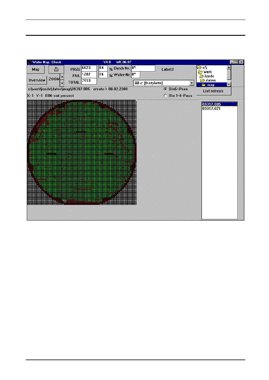
8.2.2 Wafer Mapping
Wafer mapping for failed die identification is available on Floppy-Disk.
Format:
Electroglas ESC≠ASCEND on 3.5
Floppy-Disk
NOTE: The wafer map refers to unsawn wafers. At sawn wafers (on FFC) additional ICs
might be inked (marked as fail) if damaged during the sawing process (compared to
wafer map)!
See Appendix D for an example of the wafer map.

Product Specification
SL1 ICS31 01
Rev. 1.2
July 2000
Page 12 of 22
Public
9 Quality Assurance
9.1 Electrical Acceptance Test
The electrical acceptance test is performed in line (`sampling on the fly') according to the test
specifications.
Sampling plan:
according General Quality Specification
9.2 Visual Inspection
9.2.1 After Wafer Final Test
Performed according document SNW-FQ-627.
Sampling plan:
according General Quality Specification
9.2.2 After Sawing (Film Frame Carrier)
Performed according document PICTOH-QS007.
Sampling plan (3 wafers per lot):
accept 0/3

Product Specification
SL1 ICS31 01
Rev. 1.2
July 2000
Page 13 of 22
Public
10 Packing
The packing for shipment of wafers has to protect the wafers against shock, severe impact, dust and
electrostatic discharge. The packing of unsawn wafers or sawn wafers is done according to Philips
`General Specification for 6" Wafer'.
10.1 Storage Recommendations
Unsawn/sawn wafers should be kept in their original packing whilst in storage.
Recommended storage conditions:
Temperature:
15 ... 25 ∞C
Climate atmosphere:
40 ... 60 % r.h. or dried N
2
(only unsawn wafers!)
Duration of storage:
max. 6 months
Deviating requirements have to be arranged between customer and Philips Semiconductors.
10.2 Possible Forms of Delivery
10.2.1 Packing of Unsawn Wafers
Delivery form:
wafer box
10.2.2 Packing of Sawn Wafers
Delivery form:
Film Frame Carrier (standard Philips carrier type P7)
Foil thickness:
0.55 ... 0.85 mm
Foil material:
sticky foil

Product Specification
SL1 ICS31 01
Rev. 1.2
July 2000
Page 14 of 22
Public
11 Handling Recommendations
Please refer to Philips `General Specification for 6" Wafer' for the following items:
11.1 Sawing
11.2 Die Attach
11.3 Wire Bonding
12 Coil Specification
The I∑CODE1 Label IC has to be connected at pads LA, LB to a coil characterised by its electrical
parameters according to Philips application note `I∑CODE Label IC, Coil Design Guide'.
Product Specification
SL1 ICS31 01
Rev. 1.2
July 2000
Page 15 of 22
Public
13 Electrical Specifications
ABSOLUTE MAXIMUM RATINGS
1, 2
SYMBOL
PARAMETER
TEST
CONDITIONS
RATING
UNIT
T
stg
Storage Temperature Range
- 55 to
+
140
∞C
T
j
Junction Temperature
- 55 to
+
140
∞C
V
ESD
ESD Voltage Immunity
MIL-STD-883D,
Method 3015.7,
Human Body Model
± 2
kV
peak
I
max LA-LB
Maximum Input Peak Current
3
± 80
mA
peak
NOTES:
1. Stresses above those listed under Absolute Maximum Ratings may cause permanent damage to the device. This is a stress rating
only and functional operation of the device at these or any conditions other than those described in the Operating Conditions and
Electrical Characteristics section of this specification is not implied.
2. This product includes circuitry specifically designed for the protection of its internal devices from the damaging effects of excessive
static charge. Nonetheless, it is suggested that conventional precautions be taken to avoid applying greater than the rated maxima.
3. At 13.56 MHz, including current via resonance capacitor.
OPERATING CONDITIONS
SYMBOL
PARAMETER
TEST
CONDITIONS
MIN
TYP
1
MAX
UNIT
T
amb
Operating Ambient Temperature
- 25
+
70
∞C
T
j op
Operating Junction Temperature
- 25
+
85
∞C
I
LA-LB
Input Current
2
50
mA
rms
V
LA-LB rd
Minimum Supply Voltage
3
for READ/EAS
Standard Mode
± 3.1
± 3.7
V
peak
V
LA-LB wr
Minimum Supply Voltage
3
for WRITE
Standard Mode
± 3.6
± 4.1
V
peak
V
LA-LB fm
Minimum Supply Voltage
3
for READ/EAS/WRITE
Fast Mode
± 5.2
± 6.5
V
peak
f
op
Operating Frequency
4
13.553
13.560
13.567
MHz
NOTES:
1. Typical ratings are not guaranteed. These values listed are at room temperature.
2. Including current via resonance capacitor.
3. The voltage between LA and LB is limited by the on-chip voltage limitation circuitry (corresponding to parameter I
LA-LB
).
4. Bandwidth limitation (±7 kHz) according to ISM band regulations.
ELECTRICAL CHARACTERISTICS
T
amb
= - 25 to +70 ∞C
SYMBOL
PARAMETER
TEST
CONDITIONS
MIN
TYP
1
MAX
UNIT
C
res
Input Capacitance between LA - LB
2
V
LA-LB
= 2 V
rms
92
97
102
pF
P
min
Minimum Operating Supply Power
3
V
LA-LB
= 2 V
rms
450
µW
m
min
Minimum Modulation of RF Voltage
for Demodulator Response
m
V
- V
V
+ V
max
min
max
min
=
10
14
%
m
max
Maximum Modulation of RF Voltage
for Demodulator Response
m
V
- V
V
+ V
max
min
max
min
=
30
%
t
P sm
Modulation Pulse Length
of RF Voltage
4
Standard Mode,
m
10 %
3.54
5.31
5
9.44
µs
t
P fm
Modulation Start-Pulse Length
of RF Voltage
4
Fast Mode,
m
10 %
15.34
17.11
5
20.06
µs
t
D
Demodulator Response Time
m
10 %
0.1
0.8
2.4
µs
R
mod
Modulator ON Resistance
50
115
250
t
ret
EEPROM Data Retention
T
amb
55 ∞C
10
Years
n
write
EEPROM Write Endurance
100 000
Cycles
NOTES:
1. Typical ratings are not guaranteed. These values listed are at room temperature.
2. Measured with an HP4285A LCR meter at 13.56 MHz.
3. Including losses in resonant capacitor and rectifier.
4. The given values are derived from the 13.56 MHz system frequency.
5. Recommended values for pulse duration generated at the read/write device.

Product Specification
SL1 ICS31 01
Rev. 1.2
July 2000
Page 16 of 22
Public
14 Hints for Label IC Encapsulation
14.1 Protection against Visible Light
As a result of the ultra low power design of the I∑CODE1 Label IC some analogue circuits on the
chip are light sensitive. This means that common sun light can impact the operation of the label if
the chip is not protected against visible light radiation.
Measurements have shown that a radiation of E
max
= 60 W/m
2
(spectrum: 400 to 1000 nm) causes a
reduced operating range of the plain chip.
Measurements of direct sunlight in summer deliver values up to 260 W/m
2
.
To ensure proper operation an expected minimum radiation reduction factor of approx. 9
(2 x 260/60 = 8.7) must be provided by the encapsulation. That means special care has to be taken
to ensure a sufficient light protection of the I∑CODE1 Label IC (e.g. non translucent encapsulation
or underfiller, ...) according to application requirements.
14.2 Protection against UV Light
An EEPROM memory, as it is also used in the I∑CODE1 Label IC, has some principle sensitivity to
UV light (applies to EEPROM-technology in general).
Thus strong UV exposure in the production of inlets/labels has to be avoided. UV protection has to
be ensured using appropriate assembly methods.
14.3 Resistance to X-Rays
X-ray exposure on comparable Philips ICs (with even smaller feature size) caused neither a long
term influence on the behaviour of the ICs nor on the data retention of the EEPROMs.
Product Specification
SL1 ICS31 01
Rev. 1.2
July 2000
Page 17 of 22
Public
15 Inlet/Label Characterisation and Test
15.1 Characterisation of the Inlet/Label
The parameters recommended to be characterised for the inlet/label are:
Parameter
Symbol Conditions
Threshold field strength for
UNSELECTED READ command
(standard mode)
H
TRead
UNSELECTED READ command OK
Threshold resonance frequency
f
RT
Resonance frequency @ H
TRead
No command transmitted to the inlet/label
ý
Label generates no response
ý
No modulation
Threshold field strength for WRITE
command
(standard mode)
H
TWrite
WRITE (and Verifying READ) command OK
For more detailed information on inlet /label characterisation please refer to Philips application note
`I∑CODE Label IC, Coil Design Guide'.
15.2 Final Test of the Inlet/Label
Basic flow for production and test:
1.
Production of wafer
2.
Testing of dies on wafer
3.
Writing of serial numbers and pre-configuration
4.
Sawing of wafer
5.
Assembly of inlets/labels
6.
Final test of inlets/labels
7.
Writing of customer data
To detect damage of EEPROM cells during production of inlets/labels a final test of the
EEPROM after assembly of the inlet/label is recommended. This is necessary to achieve
lowest failure rates.
Product Specification
SL1 ICS31 01
Rev. 1.2
July 2000
Page 18 of 22
Public
16 Appendix A: Die Plan
Measuring unit: µm
The two test pads (TEST and VSS) are electrically neutral at sawn wafers!
Product Specification
SL1 ICS31 01
Rev. 1.2
July 2000
Page 19 of 22
Public
17 Appendix B: Cluster Plan
Measuring unit: mm
Product Specification
SL1 ICS31 01
Rev. 1.2
July 2000
Page 20 of 22
Public
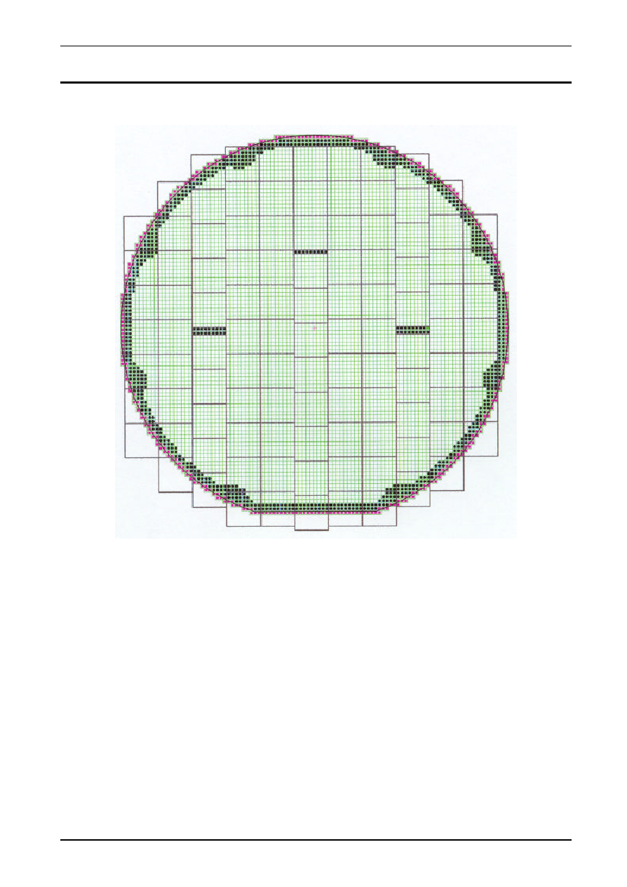
18 Appendix C: Cluster Map
The three black lines show the position of the PCM structures on the 6 inch wafer!
Product Specification
SL1 ICS31 01
Rev. 1.2
July 2000
Page 21 of 22
Public
19 Appendix D: Wafer Map
The following screenshot shows an example of a wafer map:
Map file of this example:
ELECTROGLAS APPLICATIONS - WAFER TEST DATA
FILE
COPYRIGHT
ASCEND
LOT
09397
DEVICE VCOL1HE2
PRODUCT VCOL\4020
WAFER 05
READER 09397-05-B6
XSTEP
575
UNITS
(0.1)MIL
YSTEP
587
UNITS
(0.1)MIL
XREF
16891
UNITS
(0.1)MIL
YREF
-261
UNITS
(0.1)MIL
XDELTA 0
YDELTA 0
FLAT
0
XFRST
21
YFRST
50
PRQUAD 1
COQUAD 1
DIAM
6000
UNITS
MIL
DATE
2000-01-23
TIME
15:30:00
OPERATOR
4020
SETUP FILE
M:\SET\VCOL1HE2.SET
TEST SYSTEM
SYS
VCOL\4020
TEST DATA
PROBE CARD
PC
PROBER PIWP105
:
:
### shortening of the file ###
:
:
X40Y3
3
0
X41Y3
5
1
X42Y3
5
1
X43Y3
5
1
X44Y3
5
1
X45Y3
5
1
X46Y3
5
1
X47Y3
2
0
X48Y3
2
0
X49Y3
2
0
X50Y3
5
1
X51Y3
5
1
X52Y3
5
1
X53Y3
5
1
X54Y3
5
1
:
:
### shortening of the file ###
:
:
EDATE
ETIME

Philips Semiconductors - a worldwide company
Published by:
Philips Semiconductors Gratkorn GmbH, Mikron-Weg 1, A-8101 Gratkorn, Austria, Fax: +43 3124 299 270
For all other countries apply to: Philips Semiconductors, International Marketing & Sales Communications,
Building BE-p, P.O. Box 218, 5600 MD EINDHOVEN, The Netherlands, Fax: +31 40 27 24825
Internet: http://www.semiconductors.philips.com
© Royal Philips Electronics N.V. 2000
All rights are reserved. Reproduction in whole or in part is prohibited without the prior written consent of the copyright owner.
The information presented in this document does not form part of any quotation or contract, is believed to be accurate and reliable and may be changed without notice.
No liability will be accepted by the publisher for any consequence of its use. Publication thereof does not convey nor imply any license under patent- or other industrial
or intellectual property rights.
Argentina: see South America
Australia: 34 Waterloo Road, North Ryde, NSW 2113,
Tel. +61 2 9805-4455, Fax. +61 9 9805-4466
Austria: Computerstr. 6, A-1101 WIEN, P.O. Box 213,
Tel. +43 1 60 101, Fax. +43 1 60 101 1210
Belarus: Hotel Minsk Business Center, Bld. 3, r. 1211, Volodarski
Str. 6, 220050 MINSK, Tel. +375 172 200 733, Fax. +375 172 200 773
Belgium: see The Netherlands
Brazil: see South America
Bulgaria: Philips Bulgaria Ltd., Energoproject, 15th floor, 51 James
Bourchier Blvd., 1407 SOFIA, Tel. +359 2 689 211, Fax. +359 2 689 102
Canada: see United States
China/Hong Kong: 501 Hong Kong Industrial Technology Centre, 72 Tat
Chee Avenue, Kowloon Tong, Tel. +852 2811-9111, Fax. +852 2811-9173
Colombia: see South America
Czech Republic: see Austria
Denmark: Frederikskaj, Sydhavnsgade 23, DK-1780 Copenhagen V,
Tel. +45 33 293333, Fax. +45 33 293905
Finland: Sinikalliontie 3, FIN-02630 ESPOO,
Tel. +358 9 615800, Fax. +358 9 61580/xxx
France: 51, Rue Carnot - BP317 92156 Suresnes Cedex,
Tel. +33 1 40 99 6161, Fax. +33 1 40 996427
Germany: Hammerbrookstrabe 69, D-20097 HAMBURG,
Tel. +49 40 23 53 60, Fax. +49 40 23 536 300
Greece: No. 15, 25th March Street, GR 17778 TAVROS/ATHENS,
Tel. +30 1 4894 339/239, Fax. +30 1 4814 240
Hungary: see Austria
India: Shivsagar Estate, Block 'A', Dr. Annie Besant Road, Worli,
Mumbai-400 018, Tel. +91 22 492-1365, Fax. +91 22 493-8722
Indonesia: Gedung Philips, Jl. Buncit Raya Kav. 99-100,
Jakarta 12510, Tel. +62 21 794-0040, Fax. +62 21 794-0080
Ireland: Newstead, Clonskeagh, DUBLIN 14,
Tel. +353 1 7640 000, Fax. +353 1 7640 200
Israel: RAPAC Electronics, 7 Kehilat Saloniki St,
TEL AVIV 61180, Tel. +972 3 645 0444, Fax. +972 3 648 1007
Italy: PHILIPS SEMICONDUCTORS, Piazza IV Novembre 3,
20124 MILANO, Tel. +39 2 6752 2531, Fax. +39 2 6752 2557
Japan: Philips Bldg 13-37, Kohnan 2-chome, Minato-ku,
Tokyo 108-8507, Tel. +81 3 3740-5130, Fax. +81 3 3740-5057
Korea: 260-199 Itaewon-dong, Yongsan-ku, Seoul, Korea C.,
P.O. Box 3680, Tel. +82 2 709-1412, Fax. +82 2 709-1415
Malaysia: 76 Jalan Universiti, 46200 Petaling Jaya,
Selangor, Tel. +60 3 757 5214, Fax. +60 3 757-4880
Mexico: Philips Components, El Paso, Texas, Tel. +1 915 772-4020
Middle East: see Italy
Netherlands: Postbus 90050, 5600 PB EINDHOVEN, Bldg. VB,
Tel. +31 40 27 82785, Fax. +31 40 27 88399
New Zealand: 2 Wagener Place, Mt Albert, C.P.O.Box 1041,
Auckland, Tel. +64 9 815-4144, Fax. +64 9 849-7811
Norway: Box 1, Manglerud 0612, OSLO,
Tel. +47 22 74 8000, Fax. +47 22 74 8341
Pakistan: see Singapore
Philippines: 106 Valero Street, Salcedo Village, Makati City,
Metro Manila, Tel. +63 2 816-6380, Fax. +63 2 817-3474
Poland: Ul. Lukiska 10, PL 04-123 WARSZAWA,
Tel. +48 22 612 2831, Fax. +48 22 612 2327
Portugal: see Spain
Romania: see Italy
Russia: Philips Russia, Ul. Usatcheva 35A, 119048 MOSCOW,
Tel. +7 095 755 6918, Fax. +7 095 755 6919
Singapore: Lorong One, Toa Payoh, Singapore 319762,
Tel. +65 350-2538, Fax. +65 251-6500/250-6010
Slovakia: see Austria
Slovenia: see Italy
South Africa: S.A. PHILIPS Pty Ltd., 195-215 Main Road
Martindale, 2092 JOHANNESBURG, P.O. Box 7430 Johannesburg 2000,
Tel. +27 11 470 5911, Fax. +27 11 470 5494
South America : Al. Vicente Pinzon, 173 - 6th floor,
04547-130 Sao Paulo, SP - Brazil,
Tel. +55 11 821 2333, Fax. +55 11 829 1849
Spain: Balmes 22, 08007 BARCELONA,
Tel. +34 3 301 6312, Fax. +34 3 301 4107
Sweden: Kottbygatan 7, Akalla, S-16485 STOCKHOLM,
Tel. +46 8 598 520 00, Fax. +46 8 632 2745
Switzerland: Allmendstrasse 140, CH-8027 ZÐRICH,
Tel. +41 1 488 2686, Fax. +41 1 481 7730
Taiwan R.O.C.: 6th Floor, No. 96, Chien Kuo North Road, Sec.1,
Taipei, Tel. +886 2 2134-2865, Fax. +886 2 2134-2874
Thailand: 209/2 Sanpavuth-Bangna Road, Prakanong, Bangkok 10260,
Tel. +66 2 745-4090 x3261, Fax. +66 2 398-0793
Turkey: Talatpasa Cad. No. 5, 80640 GÐLTEPE/ISTANBUL,
Tel. +90 212 279 2770, Fax. +90 212 282 6707
Ukraine: PHILIPS UKRAINE, 4 Patrice Lumumba str., Building B,
Floor 7, 252042 KIEV, Tel. +380 44 264 2776, Fax. +380 44 268 0461
United Kingdom: Philips Semiconductors Ltd., 276 Bath Road, Hayes,
MIDDLESEX UB3 5BX, Tel. +44 181 730 5000, Fax. +44 181 754 8421
United States: 811 East Arques Avenue, P.O. Box 3409, Sunnyvale,
CA 94088-3409, Tel. +800 234 7381, Fax. +800 943 0087
Uruguay: see South America
Vietnam: see Singapore
Yugoslavia: PHILIPS, Trg N. Pasica 5/v, 11000 BEOGRAD,
Tel. +381 11 625 344, Fax.+381 11 635 777