
SSTU32865
1.8 V 28-bit 1:2 registered buffer with parity
for DDR2 RDIMM applications
Rev. 01 -- 05 July 2004
Product data
1.
Description
The SSTU32865 is a 1.8 V 28-bit 1:2 register specifically designed for use on two
rank by four (2Rx4) and similar high-density DDR2 memory modules. It is similar in
function to the JEDEC-standard 14-bit DDR2 register, but integrates the functionality
of the normally required two registers in a single package, thereby freeing up board
real-estate and facilitating routing to accommodate high-density DIMM designs.
The SSTU32865 also integrates a parity function, which accepts a parity bit from the
memory controller, compares it with the data received on the D-inputs and indicates
whether a parity error has occurred on its open-drain PTYERR pin (active-LOW).
The SSTU32865 is packaged in a 160-ball, 12
�
18 grid, 0.65 mm ball pitch TFBGA
package, which--while requiring a minimum 9
�
13 mm of board space--allows for
adequate signal routing and escape using conventional card technology.
2.
Features
s
28-bit data register supporting DDR2
s
Fully compliant to JEDEC standard JESD82-9
s
Supports 2 rank by 4 DIMM density by integrating equivalent functionality of two
JEDEC-standard DDR2 registers (i.e. 2
�
SSTU32864 or 2
�
SSTU32866)
s
Parity checking function across 22 input data bits
s
Parity out signal
s
Single 1.8 V supply operation
s
Available in 160-ball 9
�
13 mm, 0.65 mm ball pitch TFBGA package
3.
Applications
s
High-density (e.g. 2 rank by 4) DDR2 registered DIMMs
s
DDR2 registered DIMMs desiring parity checking functionality
Philips Semiconductors
SSTU32865
1.8 V DDR2 registered buffer with parity
Product data
Rev. 01 -- 05 July 2004
2 of 25
9397 750 10942
� Koninklijke Philips Electronics N.V. 2004. All rights reserved.
4.
Ordering information
5.
Functional diagram
Table 1:
Ordering information
Type number
Package
Name
Description
Solder process
Version
SSTU32865ET/G
TFBGA160
plastic thin ball grid array package; 160 balls;
body 9
�
13
�
0.8 mm
Pb-free (SnAgCu solder ball
compound)
SOT802-1
SSTU32865ET
TFBGA160
plastic thin ball grid array package; 160 balls;
body 9
�
13
�
0.8 mm
SnPb solder ball compound
SOT802-1
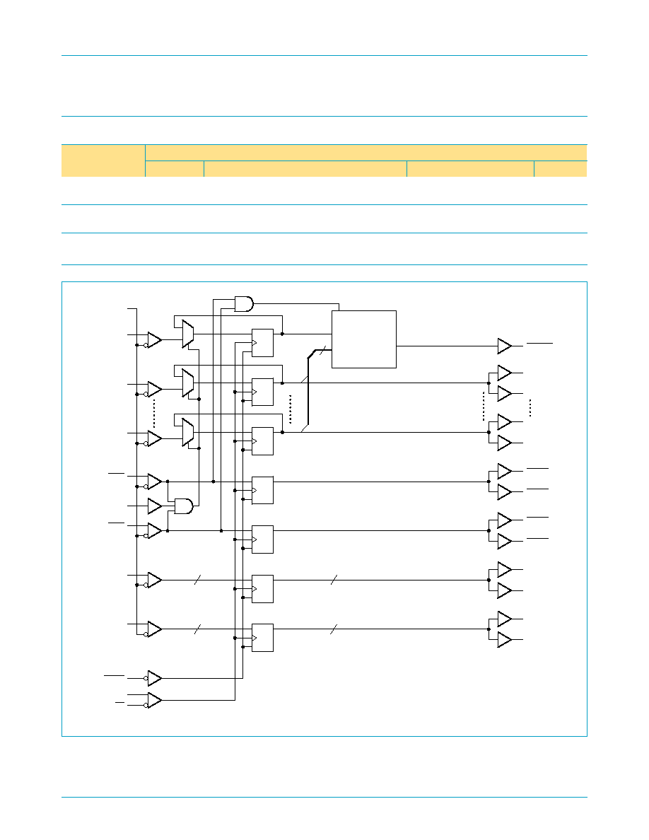
Fig 1.
SSTU32865 functional block diagram.
D
Q
R
D
Q
R
D
Q
R
D
Q
R
D
Q
R
D
Q
R
D
Q
R
PARIN
D0
D21
VREF
(CS ACTIVE)
DCS0
DCS1
DCKE0,
DCKE1
DODT0,
DODT1
CSGateEN
RESET
CK
CK
22
PARITY
GENERATOR
AND
CHECKER
Q0A
Q0B
Q21A
Q21B
QCS0A
QCS0B
QCS1A
QCS1B
QCKE0A,
QCKE1A
QCKE0B,
QCKE1B
QODT0A,
QODT1A
QODT0B,
QODT1B
PTYERR
2
2
2
2
002aaa386
Philips Semiconductors
SSTU32865
1.8 V DDR2 registered buffer with parity
Product data
Rev. 01 -- 05 July 2004
3 of 25
9397 750 10942
� Koninklijke Philips Electronics N.V. 2004. All rights reserved.
6.
Pinning information
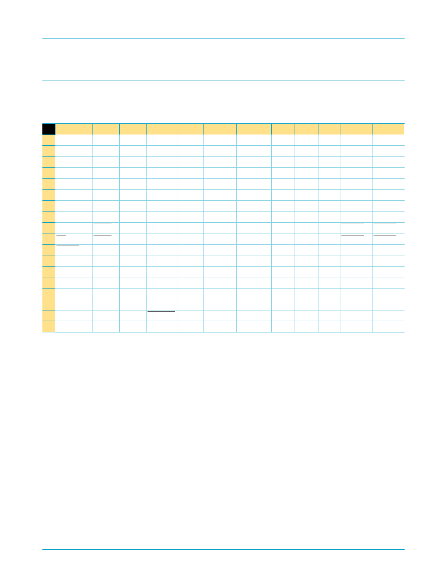
Table 2:
Ball mapping
160-ball, 12
�
18 grid; top view. An empty cell indicates no ball is populated at that grid point. NC denotes a no-connect (ball
present but not connected to the die). MCL denotes a pin that Must be Connected LOW. MCH denotes a pin that Must be
Connected HIGH.
1
2
3
4
5
6
7
8
9
10
11
12
A
VREF
NC
PARIN
NC
NC
QCKE1A
QCKE0A
Q21A
Q19A
Q18A Q17B
Q17A
B
D1
D2
NC
NC
NC
QCKE1B
QCKE0B
Q21B
Q19B
Q18B QODT0B QODT0A
C
D3
D4
QODT1B QODT1A
D
D6
D5
VDDL
GND
NC
NC
GND
GND
Q20B
Q20A
E
D7
D8
VDDL
GND
VDDL
VDDR
GND
GND
Q16B
Q16A
F
D11
D9
VDDL
GND
VDDR VDDR
Q1B
Q1A
G
D18
D12
VDDL
GND
VDDR VDDR
Q2B
Q2A
H
CSGateEN D15
VDDL
GND
GND
GND
Q5B
Q5A
J
CK
DCS0
GND
GND
VDDR VDDR
QCS0B
QCS0A
K
CK
DCS1
VDDL
VDDL
GND
GND
QCS1B
QCS1A
L
RESET
D14
GND
GND
VDDR VDDR
Q6B
Q6A
M
D0
D10
GND
GND
GND
GND
Q10B
Q10A
N
D17
D16
VDDL
VDDL
VDDR VDDR
Q9B
Q9A
P
D19
D21
GND
VDDL
VDDL
VDDR
VDDR GND
Q11B
Q11A
R
D13
D20
GND
VDDL
VDDL
GND
GND
GND
Q15B
Q15A
T
DODT1
DODT0
Q14B
Q14A
U
DCKE0
DCKE1 MCL
PTYERR MCH
Q3B
Q12B
Q7B
Q4B
Q13B Q0B
Q8B
V
VREF
MCL
MCL
NC
MCH
Q3A
Q12A
Q7A
Q4A
Q13A Q0A
Q8A

Philips Semiconductors
SSTU32865
1.8 V DDR2 registered buffer with parity
Product data
Rev. 01 -- 05 July 2004
4 of 25
9397 750 10942
� Koninklijke Philips Electronics N.V. 2004. All rights reserved.
6.1 Pin description
Table 3:
Pin description
Signal group
Signal name
Type
Description
Ungated inputs
DCKE0, DCKE1,
DODT0, DODT1
SSTL_18
DRAM function pins not associated with Chip Select.
Chip Select gated
inputs
D0-D21
SSTL_18
DRAM inputs, re-driven only when Chip Select is LOW.
Chip Select inputs
DCS0, DCS1
SSTL_18
DRAM Chip Select signals. These pins initiate DRAM
address/command decodes, and as such at least one will be LOW
when a valid address/command is present. The register can be
programmed to re-drive all D-inputs only (CSGateEN = HIGH)
when at least one Chip Select input is LOW.
Re-driven outputs
Q0A-Q21A,
Q0B-Q21B,
QCS0-1A,B,
QCKE0-1A,B,
QODT0-1A,B
SSTL_18
Outputs of the register, valid after the specified clock count and
immediately following a rising edge of the clock.
Parity input
PARIN
SSTL_18
Parity input for the D0-D21 inputs. Arrives one clock cycle after the
corresponding data input.
Parity error
PTYERR
open drain
When LOW, this output indicates that a parity error was identified
associated with the address and/or command inputs. PTYERR will
be active for two clock cycles, and delayed by an additional clock
cycle for compatibility with final parity out timing on the
industry-standard DDR2 register with parity (in JEDEC definition).
Program inputs
CSGateEN
1.8 V
LVCMOS
Chip Select Gate Enable. When HIGH, the D0-D21 inputs will be
latched only when at least one Chip Select input is LOW during the
rising edge of the clock. When LOW, the D0-D21 inputs will be
latched and redriven on every rising edge of the clock.
Clock inputs
CK, CK
SSTL_18
Differential master clock input pair to the register. The register
operation is triggered by a rising edge on the positive clock input
(CK).
Miscellaneous inputs
MCL, MCH
Must be connected to a logic LOW or HIGH.
RESET
1.8 V
LVCMOS
Asynchronous reset input. When LOW, it causes a reset of the
internal latches, thereby forcing the outputs LOW. RESET also
resets the PTYERR signal.
VREF
0.9 V
nominal
Input reference voltage for the SSTL_18 inputs. Two pins
(internally tied together) are used for increased reliability.

Philips Semiconductors
SSTU32865
1.8 V DDR2 registered buffer with parity
Product data
Rev. 01 -- 05 July 2004
5 of 25
9397 750 10942
� Koninklijke Philips Electronics N.V. 2004. All rights reserved.
7.
Functional description
7.1 Functional information
This 28-bit 1:2 registered buffer with parity is designed for 1.7 V to 1.9 V V
DD
operation.
All clock and data inputs are compatible with the JEDEC standard for SSTL_18. The
control inputs are LVCMOS. All outputs are 1.8 V CMOS drivers that have been
optimized to drive the DDR2 DIMM load.
The SSTU32865 operates from a differential clock (CK and CK). Data are registered
at the crossing of CK going HIGH, and CK going LOW.
The device supports low-power standby operation. When the reset input (RESET) is
LOW, the differential input receivers are disabled, and undriven (floating) data, clock
and reference voltage (V
REF
) inputs are allowed. In addition, when RESET is LOW all
registers are reset, and all outputs except PTYERR are forced LOW. The LVCMOS
RESET input must always be held at a valid logic HIGH or LOW level.
To ensure defined outputs from the register before a stable clock has been supplied,
RESET must be held in the LOW state during power-up.
In the DDR2 RDIMM application, RESET is specified to be completely asynchronous
with respect to CK and CK. Therefore, no timing relationship can be guaranteed
between the two. When entering reset, the register will be cleared and the data
outputs will be driven LOW quickly, relative to the time to disable the differential input
receivers. However, when coming out of reset, the register will become active quickly,
relative to the time to enable the differential input receivers. As long as the data inputs
are LOW, and the clock is stable during the time from the LOW-to-HIGH transition of
RESET until the input receivers are fully enabled, the design of the SSTU32865
ensures that the outputs remain LOW, thus ensuring no glitches on the output.
The device monitors both DCS0 and DCS1 inputs and will gate the Qn outputs from
changing states when both DCS0 and DCS1 are HIGH. If either DCS0 or DCS1 input
is LOW, the Qn outputs will function normally. The RESET input has priority over the
DCS0 and DCS1 control and will force the Qn outputs LOW and the PTYERR output
HIGH. If the DCS-control functionality is not desired, then the CSGateEnable input
can be hardwired to ground, in which case, the setup-time requirement for DCS
would be the same as for the other D data inputs.
The SSTU32865 includes a parity checking function. The SSTU32865 accepts a
parity bit from the memory controller at its input pin PARIN, compares it with the data
received on the D-inputs (with either DCS0 or DCS1 active) and indicates whether a
parity error has occurred on its open-drain PTYERR pin (active LOW).
7.2 Functional differences to SSTU32864
The SSTU32865 for its basic register functionality, signal definition and performance
is based upon the industry-standard SSTU32864, but provides key operational
features which differ (at least in part) from the industry-standard register in the
following aspects:

Philips Semiconductors
SSTU32865
1.8 V DDR2 registered buffer with parity
Product data
Rev. 01 -- 05 July 2004
6 of 25
9397 750 10942
� Koninklijke Philips Electronics N.V. 2004. All rights reserved.
7.2.1
CS gating of key inputs (DCS0, DCS1, CSGateEnable)
As a means to reduce device power, the internal latches will only be updated when
one or both of the CS inputs are active (LOW) and CSGateEnable HIGH at the rising
edge of the clock. The 22 `Chip-Select-gated' input signals associated with this
function include addresses (ADDR0-ADDR15, BA0-BA2), RAS, CAS, WE, with the
remaining signals (CS, CKE, ODT) continuously re-driven at the rising edge of every
clock as they are independent of CS. The CS gating function can be disabled by tying
CSGateEnable LOW, enabling all internal latches to be updated on every rising edge
of the clock.
7.2.2
Parity error checking and reporting
The SSTU32865 incorporates a parity function, whereby the signal received on input
pin PARIN is received as parity to the register, one clock cycle later than the
CS-gated inputs. The received parity bit is then compared to the parity calculated
across these same inputs by the register parity logic to verify that the information has
not been corrupted. The 22 CS-gated input signals will be latched and re-driven on
the first clock, and any error will be reported one clock cycle later via the PTYERR
output pin (driven LOW for two consecutive clock cycles). PTYERR is an open-drain
output, allowing multiple modules to share a common signal pin for reporting the
occurrence of a parity error during a valid command cycle (coincident with the
re-driven signals). This output is driven LOW for two consecutive clock cycles to allow
the memory controller sufficient time to sense and capture the error even. A LOW
state on PTYERR indicates that a parity error has occurred.
7.2.3
Reset (RESET)
Similar to the RESET pin on the industry-standard SSTU32864, this pin is used to
clear all internal latches and all outputs will be driven LOW quickly except the
PTYERR output, which will be floated (and will normally default HIGH by their
external pull-up).
7.2.4
Power-up sequence
The reset function for the SSTU32865 is similar to that of the SSTU32864 except that
the PTYERR signal is also cleared and will be held clear for three consecutive clock
cycles.
Table 4:
Chip Select gating mode
Mode
Signal name
Description
Gating
CSGateEnable
HIGH
Registers only re-drive signals to the DRAMs when
Chip Select inputs are LOW.
Non-gating
CSGateEnable
LOW
Registers always re-drive signals on every clock cycle,
independent of the state of the Chip Select inputs.
Philips Semiconductors
SSTU32865
1.8 V DDR2 registered buffer with parity
Product data
Rev. 01 -- 05 July 2004
7 of 25
9397 750 10942
� Koninklijke Philips Electronics N.V. 2004. All rights reserved.
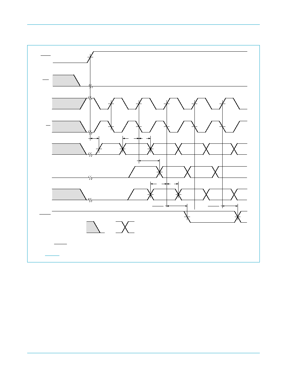
(1) After RESET is switched from LOW to HIGH, all data and PARIN input signals must be set and held LOW for a minimum
time of t
ACT
(max.) to avoid false error.
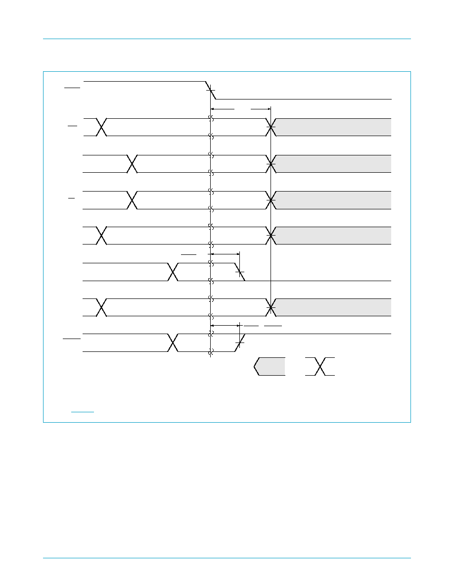
Fig 2.
RESET switches from L to H.
CK
Dn
(1)
Qn
tsu
002aaa983
CK
n
n + 1
n + 2
n + 3
n + 4
DCSn
RESET
tACT
th
tPDM, tPDMSS
CK to Q
PARIN
tsu
th
tPHL, tPLH
CK to PTYERR
tPHL
CK to PTYERR
PTYERR
H, L, or X
H or L
Philips Semiconductors
SSTU32865
1.8 V DDR2 registered buffer with parity
Product data
Rev. 01 -- 05 July 2004
8 of 25
9397 750 10942
� Koninklijke Philips Electronics N.V. 2004. All rights reserved.
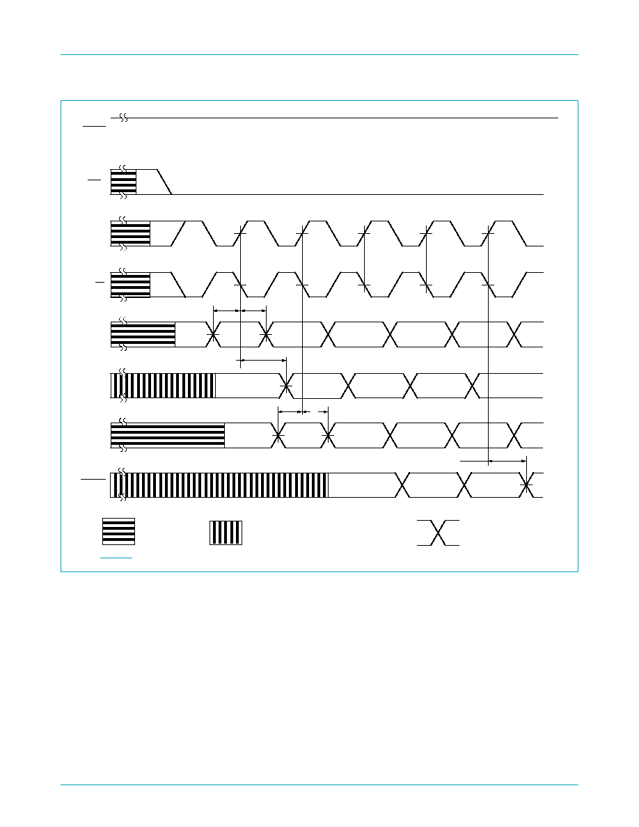
Fig 3.
RESET being held HIGH
CK
Dn
(1)
Qn
tsu
002aaa984
CK
n
n + 1
n + 2
n + 3
n + 4
DCSn
RESET
th
tPDM, tPDMSS
CK to Q
PARIN
th
tPHL, tPLH
CK to PTYERR
PTYERR
Output signal is dependent on the prior unknown event
H or L
Unknown input event
tsu
Philips Semiconductors
SSTU32865
1.8 V DDR2 registered buffer with parity
Product data
Rev. 01 -- 05 July 2004
9 of 25
9397 750 10942
� Koninklijke Philips Electronics N.V. 2004. All rights reserved.
(1) After RESET is switched from HIGH to LOW, all data and clock input signals must be set and held at valid logic levels (not
floating) for a minimum time of t
INACT
(max.).
Fig 4.
RESET switches from H to L
CK
(1)
DCSn
RESET
tINACT
tRPHL
RESET to Q
PARIN
(1)
tRPLH
RESET to PTYERR
PTYERR
H, L, or X
H or L
CK
(1)
Dn
(1)
Qn
002aaa985
Philips Semiconductors
SSTU32865
1.8 V DDR2 registered buffer with parity
Product data
Rev. 01 -- 05 July 2004
10 of 25
9397 750 10942
� Koninklijke Philips Electronics N.V. 2004. All rights reserved.
7.3 Function table
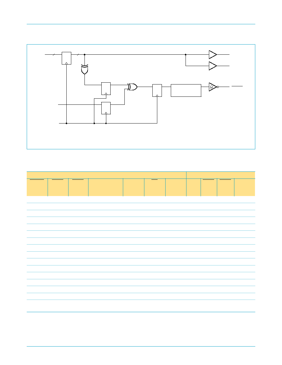
(1) This function holds the error for two cycles. For details, see
Section 7 "Functional description"
and
Figure 2 "RESET
switches from L to H."
.
Fig 5.
Parity logic diagram.
D
22
D
D
LATCHING AND
RESET FUNCTION
see Note (1)
PTYERR
D
QnA
QnB
Dn
PARIN
CLOCK
Q
002aaa417
22
Table 5:
Function table (each flip-flop)
Inputs
Outputs
RESET
DCS0
DCS1
CSGateEN
CK
CK
Dn,
DODTn,
DCKEn
Qn
QCS0
QCS1
QODTn,
QCKEn
H
L
L
X
L
L
L
L
L
H
L
L
X
H
H
L
L
H
H
L
L
X
L or H
L or H
X
Qo
Qo
Qo
Qo
H
L
H
X
L
L
L
H
L
H
L
H
X
H
H
L
H
H
H
L
H
X
L or H
L or H
X
Qo
Qo
Qo
Qo
H
H
L
X
L
L
H
L
L
H
H
L
X
H
H
H
L
H
H
H
L
X
L or H
L or H
X
Qo
Qo
Qo
Qo
H
H
H
L
L
L
H
H
L
H
H
H
L
H
H
H
H
H
H
H
H
L
L or H
L or H
X
Qo
Qo
Qo
Qo
H
H
H
H
L
Qo
H
H
L
H
H
H
H
H
Qo
H
H
H
H
H
H
H
L or H
L or H
X
Qo
Qo
Qo
Qo
L
X or
floating
X or
floating
X or floating
X or
floating
X or
floating
X or
floating
L
L
L
L

Philips Semiconductors
SSTU32865
1.8 V DDR2 registered buffer with parity
Product data
Rev. 01 -- 05 July 2004
11 of 25
9397 750 10942
� Koninklijke Philips Electronics N.V. 2004. All rights reserved.
[1]
PARIN arrives one clock cycle after the data to which it applies. All D inputs must be driven to a known state for parity to be calculated
correctly.
[2]
This transition assumes PTYERR is HIGH at the crossing of CK going HIGH and CK going LOW. If PTYERR is LOW, it stays latched
LOW for two clock cycles or until RESET is driven LOW.
CSGateEN is `don't care' for PTRERR.
Table 6:
Parity and standby function table
Inputs
Output
RESET
DCS0
DCS1
CK
CK
of inputs = H
(D0-D21)
PARIN
[1]
PTYERR
[2]
H
L
H
even
L
H
H
L
H
odd
L
L
H
L
H
even
H
L
H
L
H
odd
H
H
H
H
L
even
L
H
H
H
L
odd
L
L
H
H
L
even
H
L
H
H
L
odd
H
H
H
H
H
X
X
PTYERR
0
H
X
X
L or H
L or H
X
X
PTYERR
0
L
X or floating
X or floating
X or floating
X or floating
X or floating
X or floating
H

Philips Semiconductors
SSTU32865
1.8 V DDR2 registered buffer with parity
Product data
Rev. 01 -- 05 July 2004
12 of 25
9397 750 10942
� Koninklijke Philips Electronics N.V. 2004. All rights reserved.
8.
Limiting values
[1]
Stresses beyond those listed under `absolute maximum ratings' may cause permanent damage to the device. These are stress ratings
only and functional operation of the device at these or any other conditions beyond those indicated under `recommended operating
conditions' is not implied. Exposure to absolute-maximum-rated conditions for extended periods may affect device reliability.
[2]
The input and output negative-voltage ratings may be exceeded if the input and output current ratings are observed.
9.
Recommended operating conditions
[1]
The RESET input of the device must be held at valid logic levels (not floating) to ensure proper device operation. The differential inputs
must not be floating, unless RESET is LOW.
Table 7:
Limiting values
In accordance with the Absolute Maximum Rating System (IEC 60134).
Symbol
Parameter
Conditions
Min
Max
Unit
V
DD
supply voltage
-
0.5
+2.5
V
V
i
receiver input voltage
[2]
-
0.5
+2.5
V
V
o
driver output voltage
[2]
-
0.5
V
DD
+ 0.5
V
I
IK
input clamp current
V
i
< 0 V or V
i
> V
DD
-
-
50
mA
I
OK
output clamp current
V
o
< 0 V or V
o
> V
DD
-
�
50
mA
I
O
continuous output current
0 V < V
o
< V
DD
-
�
50
mA
I
CCC
continuous current through
each V
DD
or GND pin
-
�
100
mA
T
stg
storage temperature
-
65
+150
�
C
ESD
HBM
electrostatic discharge
Human Body Model; 1.5 k
; 100 pF
>2
-
kV
ESD
MM
electrostatic discharge
Machine Model; 0
; 200 pF
>200
-
V
Table 8:
Recommended operating conditions
Symbol
Parameter
Conditions
Min
Nom
Max
Unit
V
DD
supply voltage
1.7
-
1.9
V
V
REF
reference voltage
0.49
�
V
DD
0.50
�
V
DD
0.51
�
V
DD
V
V
TT
termination voltage
V
REF
-
40 mV
V
REF
V
REF
+ 40 mV
V
V
i
input voltage
0
-
V
DD
V
V
IH
AC HIGH-level input voltage
Data inputs
V
REF
+ 250 mV
-
-
V
V
IL
AC LOW-level input voltage
Data inputs
-
-
V
REF
-
250 mV
V
V
IH
DC HIGH-level input voltage
Data inputs
V
REF
+ 125 mV
-
-
V
V
IL
DC LOW-level input voltage
Data inputs
-
-
V
REF
-
125 mV
V
V
IH
HIGH-level input voltage
RESET
0.65
�
V
DD
-
-
V
V
IL
LOW-level input voltage
RESET
-
-
0.35
�
V
DD
V
V
ICR
common mode input voltage
range
CK, CK
0.675
-
1.125
V
V
ID
differential input voltage
CK, CK
600
-
-
mV
I
OH
HIGH-level output current
-
-
-
8
mA
I
OL
LOW-level output current
-
-
8
mA
T
amb
operating ambient temperature
in free air
0
-
+70
�
C
Philips Semiconductors
SSTU32865
1.8 V DDR2 registered buffer with parity
Product data
Rev. 01 -- 05 July 2004
13 of 25
9397 750 10942
� Koninklijke Philips Electronics N.V. 2004. All rights reserved.
10. Static characteristics
Table 9:
DC electrical characteristics
Over recommended operating conditions, unless otherwise noted.
Symbol
Parameter
Conditions
Min
Typ
Max
Unit
V
OH
HIGH-level output voltage
I
OH
=
-
6 mA; V
DD
= 1.7 V
1.2
-
-
V
V
OL
LOW-level output voltage
I
OL
= 6 mA; V
DD
= 1.7 V
-
-
0.5
V
I
i
input current
all inputs; V
i
= V
DD
or GND;
V
DD
= 1.9 V
-
-
�
5
�
A
I
DD
static standby current
RESET = GND; V
DD
= 1.9 V
-
-
100
�
A
static operating current
RESET = V
DD
; V
DD
= 1.9 V;
V
i
= V
IH(AC)
or V
IL(AC)
-
-
40
mA
I
DDD
dynamic operating current,
clock only
RESET = V
DD
;
V
i
= V
IH(AC)
or V
IL(AC)
; CK and CK
switching at 50% duty cycle.
I
o
= 0; V
DD
= 1.8 V
-
TBD
-
�
A /
MHz
dynamic operating current,
per each data input
RESET = V
DD
;
V
i
= V
IH(AC)
or V
IL(AC)
; CK and CK
switching at 50% duty cycle. One
data input switching at half clock
frequency, 50% duty cycle. I
o
= 0;
V
DD
= 1.8 V
-
TBD
-
�
A /
MHz
C
i
input capacitance, data inputs
V
i
= V
REF
�
250 mV; V
DD
= 1.8 V
2.5
-
3.5
pF
input capacitance, CK and CK
V
ICR
= 0.9 V; V
ID)
= 600 mV;
V
DD
= 1.8 V
2
-
3
pF
input capacitance, RESET
V
i
= V
DD
or GND; V
DD
= 1.8 V
3
-
5
pF

Philips Semiconductors
SSTU32865
1.8 V DDR2 registered buffer with parity
Product data
Rev. 01 -- 05 July 2004
14 of 25
9397 750 10942
� Koninklijke Philips Electronics N.V. 2004. All rights reserved.
11. Dynamic characteristics
[1]
This parameter is not necessarily production tested.
[2]
Data inputs must be active below a minimum time of t
ACT
(max) after RESET is taken HIGH.
[3]
Data and clock inputs must be held at valid levels (not floating) a minimum time of t
INACT
(max) after RESET is taken LOW.
[1]
Includes 350 ps of test-load transmission line delay.
[2]
This parameter is not necessarily production tested.
[1]
Difference between dV/dt_r (rising edge rate) and dV/dt_f (falling edge rate).
Table 10:
Timing requirements
Over recommended operating conditions, unless otherwise noted.
Symbol
Parameter
Conditions
Min
Typ
Max
Unit
f
CLOCK
clock frequency
-
-
270
MHz
t
W
pulse duration, CK, CK HIGH or
LOW
1
-
-
ns
t
ACT
differential inputs active time
[1]
,
[2]
-
-
10
ns
t
INACT
differential inputs inactive time
[1]
,
[3]
-
-
15
ns
t
SU
set-up time, Chip Select
Chip Select valid before
clock switching
0.7
-
-
ns
set-up time, Data
Dn valid before clock
switching
0.5
-
-
ns
set-up time, PARIN
PARIN before CK and CK
0.5
-
-
ns
t
H
hold time
input to remain valid after
clock switching
0.5
-
-
ns
hold time, PARIN
PARIN after CK and CK
0.5
-
-
ns
Table 11:
Switching characteristics
Over recommended operating conditions, unless otherwise noted.
Symbol
Parameter
Conditions
Min
Typ
Max
Unit
f
MAX
maximum input clock frequency
270
-
-
MHz
t
PDM
propagation delay
clock to output
[1]
1.41
-
2.15
ns
t
LH
LOW-to-HIGH delay
CK and CK to PTYERR
1.2
-
3
ns
t
HL
HIGH-to-LOW delay
CK and CK to PTYERR
1
-
3
ns
t
PLH
LOW-to-HIGH propagation delay
from RESET to PTYERR
-
-
3
ns
t
PDMSS
propagation delay, simultaneous
switching
clock to output
[1]
,
[2]
-
-
2.35
ns
t
PHL
propagation delay
reset to output
-
-
3
ns
Table 12:
Output edge rates
Over recommended operating conditions, unless otherwise noted.
Symbol
Parameter
Conditions
Min
Typ
Max
Unit
dV/dt_r
rising edge slew rate
1
-
4
V/ns
dV/dt_f
falling edge slew rate
1
-
4
V/ns
dV/dt_
[1]
absolute difference between dV/dt_r
and dV/dt_f
-
-
1
V/ns
Philips Semiconductors
SSTU32865
1.8 V DDR2 registered buffer with parity
Product data
Rev. 01 -- 05 July 2004
15 of 25
9397 750 10942
� Koninklijke Philips Electronics N.V. 2004. All rights reserved.
12. Test information
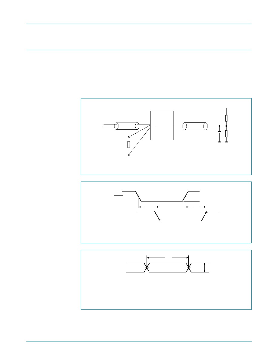
12.1 Test circuit
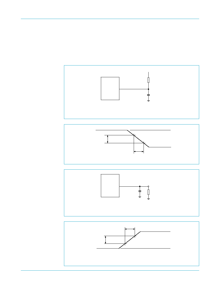
All input pulses are supplied by generators having the following characteristics:
PRR
10 MHz; Z
o
= 50
; input slew rate = 1 V/ns
�
20%, unless otherwise
specified.
The outputs are measured one at a time with one transition per measurement.
(1) C
L
includes probe and jig capacitance.
Fig 6.
Load circuit.
I
DD
tested with clock and data inputs held at V
DD
or GND, and I
o
= 0 mA.
Fig 7.
Voltage and current waveforms; inputs active and inactive times.
V
ID
= 600 mV
V
IH
= V
REF
+ 250 mV (AC voltage levels) for differential inputs. V
IH
= V
DD
for LVCMOS inputs.
V
IL
= V
REF
-
250 mV (AC voltage levels) for differential inputs. V
IL
= GND for LVCMOS inputs.
Fig 8.
Voltage waveforms; pulse duration.
RL = 100
RL = 1000
VDD
TL = 50
CK INPUTS
CK
CK
OUT
DUT
TEST POINT
002aaa371
TEST POINT
TL = 350 ps, 50
RL = 1000
CL = 30 pF
SEE NOTE (1)
LVCMOS
RESET
10%
IDD
(SEE NOTE)
tinact
VDD
VDD/2
tact
90%
0 V
002aaa372
VDD/2
VICR
VICR
VIH
VIL
INPUT
tW
VID
002aaa373

Philips Semiconductors
SSTU32865
1.8 V DDR2 registered buffer with parity
Product data
Rev. 01 -- 05 July 2004
16 of 25
9397 750 10942
� Koninklijke Philips Electronics N.V. 2004. All rights reserved.
V
ID
= 600 mV
V
REF
= V
DD
/2
V
IH
= V
REF
+ 250 mV (AC voltage levels) for differential inputs. V
IH
= V
DD
for LVCMOS inputs.
V
IL
= V
REF
-
250 mV (AC voltage levels) for differential inputs. V
IL
= GND for LVCMOS inputs.
Fig 9.
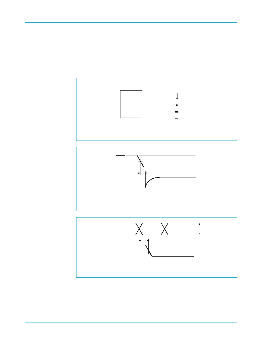
Voltage waveforms; set-up and hold times.
t
PLH
and t
PHL
are the same as t
PD
.
Fig 10. Voltage waveforms; propagation delay times.
t
PLH
and t
PHL
are the same as t
PD
.
V
IH
= V
REF
+ 250 mV (AC voltage levels) for differential inputs. V
IH
= V
DD
for LVCMOS inputs.
V
IL
= V
REF
-
250 mV (AC voltage levels) for differential inputs. V
IL
= GND for LVCMOS inputs.
Fig 11. Voltage waveforms; propagation delay times.
tsu
VIH
VIL
VID
th
CK
CK
INPUT
VREF
VREF
VICR
002aaa374
VOH
VOL
OUTPUT
tPLH
002aaa375
VTT
VICR
VICR
tPHL
CK
CK
Vi(p-p)
tPHL
002aaa376
LVCMOS RESET
INPUT
OUTPUT
VTT
VDD/2
VIH
VIL
VOH
VOL
Philips Semiconductors
SSTU32865
1.8 V DDR2 registered buffer with parity
Product data
Rev. 01 -- 05 July 2004
17 of 25
9397 750 10942
� Koninklijke Philips Electronics N.V. 2004. All rights reserved.
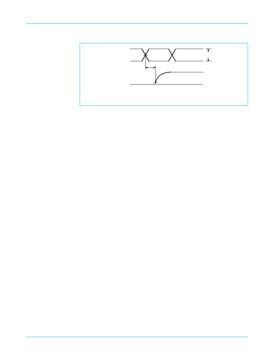
12.2 Output slew rate measurement
V
DD
= 1.8 V
�
0.1 V.
All input pulses are supplied by generators having the following characteristics:
PRR
10 MHz; Z
o
= 50
; input slew rate = 1 V/ns
�
20%, unless otherwise
specified.
(1) C
L
includes probe and jig capacitance.
Fig 12. Load circuit, HIGH-to-LOW slew measurement.
Fig 13. Voltage waveforms, HIGH-to-LOW slew rate measurement.
(1) C
L
includes probe and jig capacitance.
Fig 14. Load circuit, LOW-to-HIGH slew measurement.
Fig 15. Voltage waveforms, LOW-to-HIGH slew rate measurement.
CL = 10 pF
SEE NOTE (1)
VDD
OUT
DUT
TEST POINT
RL = 50
002aaa377
VOH
VOL
OUTPUT
80%
20%
dv_f
dt_f
002aaa378
CL = 10 pF
SEE NOTE (1)
OUT
DUT
TEST POINT
RL = 50
002aaa379
VOH
VOL
80%
20%
dv_r
dt_r
OUTPUT
002aaa380
Philips Semiconductors
SSTU32865
1.8 V DDR2 registered buffer with parity
Product data
Rev. 01 -- 05 July 2004
18 of 25
9397 750 10942
� Koninklijke Philips Electronics N.V. 2004. All rights reserved.
12.3 Error output load circuit and voltage measurement
V
DD
= 1.8 V
�
0.1 V.
All input pulses are supplied by generators having the following characteristics:
PRR
10 MHz; Z
o
= 50
; input slew rate = 1 V/ns
�
20%, unless otherwise
specified.
(1) C
L
includes probe and jib capacitance.
Fig 16. Load circuit, error output measurements.
Fig 17. Voltage waveforms, open-drain output LOW-to-HIGH transition time with
respect to RESET input.
Fig 18. Voltage waveforms, open-drain output HIGH-to-LOW transition time with
respect to clock inputs.
CL = 10 pF
SEE NOTE (1)
VDD
OUT
DUT
TEST POINT
RL = 1 k
002aaa500
VCC/2
tPLH
VCC
0 V
0.15 V
VOH
0 V
Output
Waveform 2
LVCMOS
RESET
Input
002aaa501
VICR
tHL
VCC/2
VCC
VOL
Timing
Inputs
Output
Waveform 1
Vi(p-p)
VICR
002aaa502
Philips Semiconductors
SSTU32865
1.8 V DDR2 registered buffer with parity
Product data
Rev. 01 -- 05 July 2004
19 of 25
9397 750 10942
� Koninklijke Philips Electronics N.V. 2004. All rights reserved.
Fig 19. Voltage waveforms, open-drain output LOW-to-HIGH transition time with
respect to clock inputs.
VICR
tLH
VOH
0 V
Timing
Inputs
Output
Waveform 2
VI(PP)
VICR
0.15 V
002aaa503

Philips Semiconductors
SSTU32865
1.8 V DDR2 registered buffer with parity
Product data
Rev. 01 -- 05 July 2004
20 of 25
9397 750 10942
� Koninklijke Philips Electronics N.V. 2004. All rights reserved.
13. Package outline
Fig 20. TFBGA160 package outline (SOT802-1).
UNIT
A
max.
A
1
A
2
b
e
y
w
v
REFERENCES
OUTLINE
VERSION
EUROPEAN
PROJECTION
ISSUE DATE
IEC
JEDEC
JEITA
mm
1.2
0.35
0.25
0.85
0.75
0.45
0.35
13.1
12.9
0.65
e
1
7.15
e
2
11.05
0.08
0.1
y
1
0.1
0.15
DIMENSIONS (mm are the original dimensions)
SOT802-1
- - -
- - -
- - -
03-01-29
D
E
9.1
8.9
A
detail X
A2 A1
D
V
U
T
R
P
N
M
L
K
J
H
G
F
E
D
C
A
B
1
2
3
4
5
6
7
8
9
10
11
12
E
ball A1
index area
ball A1
index area
0
5
10 mm
scale
TFBGA160: plastic thin fine-pitch ball grid array package; 160 balls; body 9 x 13 x 0.8 mm
SOT802-1
y
y1 C
1/2e
1/2e
e
e
b
C
B
A
A
C
C
B
v
M
w
M
e1
e2
X

Philips Semiconductors
SSTU32865
1.8 V DDR2 registered buffer with parity
Product data
Rev. 01 -- 05 July 2004
21 of 25
9397 750 10942
� Koninklijke Philips Electronics N.V. 2004. All rights reserved.
14. Soldering
14.1 Introduction to soldering surface mount packages
This text gives a very brief insight to a complex technology. A more in-depth account
of soldering ICs can be found in our
Data Handbook IC26; Integrated Circuit
Packages (document order number 9398 652 90011).
There is no soldering method that is ideal for all surface mount IC packages. Wave
soldering can still be used for certain surface mount ICs, but it is not suitable for fine
pitch SMDs. In these situations reflow soldering is recommended. In these situations
reflow soldering is recommended.
14.2 Reflow soldering
Reflow soldering requires solder paste (a suspension of fine solder particles, flux and
binding agent) to be applied to the printed-circuit board by screen printing, stencilling
or pressure-syringe dispensing before package placement. Driven by legislation and
environmental forces the worldwide use of lead-free solder pastes is increasing.
Several methods exist for reflowing; for example, convection or convection/infrared
heating in a conveyor type oven. Throughput times (preheating, soldering and
cooling) vary between 100 and 200 seconds depending on heating method.
Typical reflow peak temperatures range from 215 to 270
�
C depending on solder
paste material. The top-surface temperature of the packages should preferably be
kept:
�
below 225
�
C (SnPb process) or below 245
�
C (Pb-free process)
� for all BGA, HTSSON..T and SSOP..T packages
� for packages with a thickness
2.5 mm
� for packages with a thickness < 2.5 mm and a volume
350 mm
3
so called
thick/large packages.
�
below 240
�
C (SnPb process) or below 260
�
C (Pb-free process) for packages with
a thickness < 2.5 mm and a volume < 350 mm
3
so called small/thin packages.
Moisture sensitivity precautions, as indicated on packing, must be respected at all
times.
14.3 Wave soldering
Conventional single wave soldering is not recommended for surface mount devices
(SMDs) or printed-circuit boards with a high component density, as solder bridging
and non-wetting can present major problems.
To overcome these problems the double-wave soldering method was specifically
developed.
If wave soldering is used the following conditions must be observed for optimal
results:
�
Use a double-wave soldering method comprising a turbulent wave with high
upward pressure followed by a smooth laminar wave.

Philips Semiconductors
SSTU32865
1.8 V DDR2 registered buffer with parity
Product data
Rev. 01 -- 05 July 2004
22 of 25
9397 750 10942
� Koninklijke Philips Electronics N.V. 2004. All rights reserved.
�
For packages with leads on two sides and a pitch (e):
� larger than or equal to 1.27 mm, the footprint longitudinal axis is preferred to be
parallel to the transport direction of the printed-circuit board;
� smaller than 1.27 mm, the footprint longitudinal axis must be parallel to the
transport direction of the printed-circuit board.
The footprint must incorporate solder thieves at the downstream end.
�
For packages with leads on four sides, the footprint must be placed at a 45
�
angle
to the transport direction of the printed-circuit board. The footprint must
incorporate solder thieves downstream and at the side corners.
During placement and before soldering, the package must be fixed with a droplet of
adhesive. The adhesive can be applied by screen printing, pin transfer or syringe
dispensing. The package can be soldered after the adhesive is cured.
Typical dwell time of the leads in the wave ranges from 3 to 4 seconds at 250
�
C or
265
�
C, depending on solder material applied, SnPb or Pb-free respectively.
A mildly-activated flux will eliminate the need for removal of corrosive residues in
most applications.
14.4 Manual soldering
Fix the component by first soldering two diagonally-opposite end leads. Use a low
voltage (24 V or less) soldering iron applied to the flat part of the lead. Contact time
must be limited to 10 seconds at up to 300
�
C.
When using a dedicated tool, all other leads can be soldered in one operation within
2 to 5 seconds between 270 and 320
�
C.
14.5 Package related soldering information
[1]
For more detailed information on the BGA packages refer to the
(LF)BGA Application Note
(AN01026); order a copy from your Philips Semiconductors sales office.
[2]
All surface mount (SMD) packages are moisture sensitive. Depending upon the moisture content, the
maximum temperature (with respect to time) and body size of the package, there is a risk that internal
or external package cracks may occur due to vaporization of the moisture in them (the so called
popcorn effect). For details, refer to the Drypack information in the
Data Handbook IC26; Integrated
Circuit Packages; Section: Packing Methods.
Table 13:
Suitability of surface mount IC packages for wave and reflow soldering
methods
Package
[1]
Soldering method
Wave
Reflow
[2]
BGA, HTSSON..T
[3]
, LBGA, LFBGA, SQFP,
SSOP..T
[3]
, TFBGA, USON, VFBGA
not suitable
suitable
DHVQFN, HBCC, HBGA, HLQFP, HSO, HSOP,
HSQFP, HSSON, HTQFP, HTSSOP, HVQFN,
HVSON, SMS
not suitable
[4]
suitable
PLCC
[5]
, SO, SOJ
suitable
suitable
LQFP, QFP, TQFP
not recommended
[5][6]
suitable
SSOP, TSSOP, VSO, VSSOP
not recommended
[7]
suitable
CWQCCN..L
[8]
, PMFP
[9]
, WQCCN..L
[8]
not suitable
not suitable

Philips Semiconductors
SSTU32865
1.8 V DDR2 registered buffer with parity
Product data
Rev. 01 -- 05 July 2004
23 of 25
9397 750 10942
� Koninklijke Philips Electronics N.V. 2004. All rights reserved.
[3]
These transparent plastic packages are extremely sensitive to reflow soldering conditions and must
on no account be processed through more than one soldering cycle or subjected to infrared reflow
soldering with peak temperature exceeding 217
�
C
�
10
�
C measured in the atmosphere of the reflow
oven. The package body peak temperature must be kept as low as possible.
[4]
These packages are not suitable for wave soldering. On versions with the heatsink on the bottom
side, the solder cannot penetrate between the printed-circuit board and the heatsink. On versions with
the heatsink on the top side, the solder might be deposited on the heatsink surface.
[5]
If wave soldering is considered, then the package must be placed at a 45
�
angle to the solder wave
direction. The package footprint must incorporate solder thieves downstream and at the side corners.
[6]
Wave soldering is suitable for LQFP, QFP and TQFP packages with a pitch (e) larger than 0.8 mm; it
is definitely not suitable for packages with a pitch (e) equal to or smaller than 0.65 mm.
[7]
Wave soldering is suitable for SSOP, TSSOP, VSO and VSOP packages with a pitch (e) equal to or
larger than 0.65 mm; it is definitely not suitable for packages with a pitch (e) equal to or smaller than
0.5 mm.
[8]
Image sensor packages in principle should not be soldered. They are mounted in sockets or delivered
pre-mounted on flex foil. However, the image sensor package can be mounted by the client on a flex
foil by using a hot bar soldering process. The appropriate soldering profile can be provided on
request.
[9]
Hot bar soldering or manual soldering is suitable for PMFP packages.
15. Revision history
Table 14:
Revision history
Rev Date
CPCN
Description
01
20040705
-
Product data (9397 750 10942).

9397 750 10942
Philips Semiconductors
SSTU32865
1.8 V DDR2 registered buffer with parity
� Koninklijke Philips Electronics N.V. 2004. All rights reserved.
Product data
Rev. 01 -- 05 July 2004
24 of 25
Contact information
For additional information, please visit http://www.semiconductors.philips.com.
For sales office addresses, send e-mail to: sales.addresses@www.semiconductors.philips.com.
Fax: +31 40 27 24825
16. Data sheet status
[1]
Please consult the most recently issued data sheet before initiating or completing a design.
[2]
The product status of the device(s) described in this data sheet may have changed since this data sheet was published. The latest information is available on the Internet at
URL http://www.semiconductors.philips.com.
[3]
For data sheets describing multiple type numbers, the highest-level product status determines the data sheet status.
17. Definitions
Short-form specification -- The data in a short-form specification is
extracted from a full data sheet with the same type number and title. For
detailed information see the relevant data sheet or data handbook.
Limiting values definition -- Limiting values given are in accordance with
the Absolute Maximum Rating System (IEC 60134). Stress above one or
more of the limiting values may cause permanent damage to the device.
These are stress ratings only and operation of the device at these or at any
other conditions above those given in the Characteristics sections of the
specification is not implied. Exposure to limiting values for extended periods
may affect device reliability.
Application information -- Applications that are described herein for any
of these products are for illustrative purposes only. Philips Semiconductors
make no representation or warranty that such applications will be suitable for
the specified use without further testing or modification.
18. Disclaimers
Life support -- These products are not designed for use in life support
appliances, devices, or systems where malfunction of these products can
reasonably be expected to result in personal injury. Philips Semiconductors
customers using or selling these products for use in such applications do so
at their own risk and agree to fully indemnify Philips Semiconductors for any
damages resulting from such application.
Right to make changes -- Philips Semiconductors reserves the right to
make changes in the products - including circuits, standard cells, and/or
software - described or contained herein in order to improve design and/or
performance. When the product is in full production (status `Production'),
relevant changes will be communicated via a Customer Product/Process
Change Notification (CPCN). Philips Semiconductors assumes no
responsibility or liability for the use of any of these products, conveys no
licence or title under any patent, copyright, or mask work right to these
products, and makes no representations or warranties that these products are
free from patent, copyright, or mask work right infringement, unless otherwise
specified.
Level
Data sheet status
[1]
Product status
[2][3]
Definition
I
Objective data
Development
This data sheet contains data from the objective specification for product development. Philips
Semiconductors reserves the right to change the specification in any manner without notice.
II
Preliminary data
Qualification
This data sheet contains data from the preliminary specification. Supplementary data will be published
at a later date. Philips Semiconductors reserves the right to change the specification without notice, in
order to improve the design and supply the best possible product.
III
Product data
Production
This data sheet contains data from the product specification. Philips Semiconductors reserves the
right to make changes at any time in order to improve the design, manufacturing and supply. Relevant
changes will be communicated via a Customer Product/Process Change Notification (CPCN).

� Koninklijke Philips Electronics N.V. 2004.
Printed in the U.S.A.
All rights are reserved. Reproduction in whole or in part is prohibited without the prior
written consent of the copyright owner.
The information presented in this document does not form part of any quotation or
contract, is believed to be accurate and reliable and may be changed without notice. No
liability will be accepted by the publisher for any consequence of its use. Publication
thereof does not convey nor imply any license under patent- or other industrial or
intellectual property rights.
Date of release: 05 July 2004
Document order number: 9397 750 10942
Contents
Philips Semiconductors
SSTU32865
1.8 V DDR2 registered buffer with parity
1
Description . . . . . . . . . . . . . . . . . . . . . . . . . . . . . 1
2
Features . . . . . . . . . . . . . . . . . . . . . . . . . . . . . . . 1
3
Applications . . . . . . . . . . . . . . . . . . . . . . . . . . . . 1
4
Ordering information . . . . . . . . . . . . . . . . . . . . . 2
5
Functional diagram . . . . . . . . . . . . . . . . . . . . . . 2
6
Pinning information . . . . . . . . . . . . . . . . . . . . . . 3
6.1
Pin description . . . . . . . . . . . . . . . . . . . . . . . . . 4
7
Functional description . . . . . . . . . . . . . . . . . . . 5
7.1
Functional information . . . . . . . . . . . . . . . . . . . 5
7.2
Functional differences to SSTU32864 . . . . . . . 5
7.2.1
CS gating of key inputs (DCS0,
DCS1, CSGateEnable) . . . . . . . . . . . . . . . . . . 6
7.2.2
Parity error checking and reporting. . . . . . . . . . 6
7.2.3
Reset (RESET) . . . . . . . . . . . . . . . . . . . . . . . . . 6
7.2.4
Power-up sequence . . . . . . . . . . . . . . . . . . . . . 6
7.3
Function table . . . . . . . . . . . . . . . . . . . . . . . . . 10
8
Limiting values. . . . . . . . . . . . . . . . . . . . . . . . . 12
9
Recommended operating conditions. . . . . . . 12
10
Static characteristics. . . . . . . . . . . . . . . . . . . . 13
11
Dynamic characteristics . . . . . . . . . . . . . . . . . 14
12
Test information . . . . . . . . . . . . . . . . . . . . . . . . 15
12.1
Test circuit. . . . . . . . . . . . . . . . . . . . . . . . . . . . 15
12.2
Output slew rate measurement. . . . . . . . . . . . 17
12.3
Error output load circuit and voltage
measurement . . . . . . . . . . . . . . . . . . . . . . . . 18
13
Package outline . . . . . . . . . . . . . . . . . . . . . . . . 20
14
Soldering . . . . . . . . . . . . . . . . . . . . . . . . . . . . . 21
14.1
Introduction to soldering surface mount
packages . . . . . . . . . . . . . . . . . . . . . . . . . . . . 21
14.2
Reflow soldering . . . . . . . . . . . . . . . . . . . . . . . 21
14.3
Wave soldering . . . . . . . . . . . . . . . . . . . . . . . . 21
14.4
Manual soldering . . . . . . . . . . . . . . . . . . . . . . 22
14.5
Package related soldering information . . . . . . 22
15
Revision history . . . . . . . . . . . . . . . . . . . . . . . . 23
16
Data sheet status . . . . . . . . . . . . . . . . . . . . . . . 24
17
Definitions . . . . . . . . . . . . . . . . . . . . . . . . . . . . 24
18
Disclaimers . . . . . . . . . . . . . . . . . . . . . . . . . . . . 24