Document Outline
- FEATURES
- DESCRIPTION
- PIN CONFIGURATION
- QUICK REFERENCE DATA
- ORDERING INFORMATION
- PIN DESCRIPTION
- LOGIC DIAGRAM
- FUNCTION TABLE
- BALL CONFIGURATION
- ABSOLUTE MAXIMUM RATINGS 1
- RECOMMENDED OPERATING CONDITIONS 1
- DC ELECTRICAL CHARACTERISTICSÑPC1600-PC2700
- DC ELECTRICAL CHARACTERISTICSÑPC3200
- TIMING REQUIREMENTSÑPC1600-PC2700
- TIMING REQUIREMENTSÑPC3200
- SWITCHING CHARACTERISTICSÑPC1600-PC2700
- SWITCHING CHARACTERISTICSÑPC3200
- PARAMETER MEASUREMENT INFORMATION
- AC WAVEFORMS
- TEST CIRCUIT
- PACKAGE OUTLINE
- SOT362-1
- SOT480-1
- SOT702-1
- REVISION HISTORY
- Data sheet status
- Definitions
- Disclaimers
Philips
Semiconductors
SSTVF16857
DDR PC1600-PC3200 14-bit
SSTL_2 registered driver with
differential clock inputs
Product data
2003 Sep 19
INTEGRATED CIRCUITS
Philips Semiconductors
Product data
SSTVF16857
DDR PC1600-PC3200 14-bit SSTL_2 registered
driver with differential clock inputs
2
2003 Sep 19
FEATURES
∑
Stub-series terminated logic for 2.5 V V
DDQ
(SSTL_2)
∑
Optimized for PC 2700 DDR (Double Data Rate) SDRAM
applications
∑
Suitable for PC1600/PC2100 DDR SDRAM applications
∑
Suitable for PC3200 applications when used at V
DD
= 2.6 V
∑
Inputs compatible with JESD8-9 SSTL_2 specifications.
∑
Flow-through architecture optimizes PCB layout
∑
ESD classification testing is done to JEDEC Standard JESD22.
Protection exceeds 2000 V to HBM per method A114.
∑
Latch-up testing is done to JEDEC Standard JESD78, which
exceeds 100 mA.
∑
Full DDR300/333/400 solution @ 2.5V when used with PCKV857
∑
Available in TSSOP-48, TVSOP-48 and 56 ball VFBGA packages
∑
Superior VREF noise rejection
DESCRIPTION
The SSTVF16857 is a 14-bit SSTL_2 registered driver with
differential clock inputs, designed to operate between 2.3 V and
2.7 V. V
DDQ
must not exceed V
CC
. Inputs are SSTL_2 type with
V
REF
normally at 0.5*V
DDQ
. The outputs support class I which can
be used for standard stub-series applications or capacitive loads.
Master reset (RESET) asynchronously resets all registers to zero.
The SSTVF16857 is intended to be incorporated into standard
DIMM (Dual In-Line Memory Module) designs defined by JEDEC,
such as DDR (Double Data Rate) SDRAM or SDRAM II Memory
Modules. Different from traditional SDRAM, DDR SDRAM transfers
data on both clock edges (rising and falling), thus doubling the peak
bus bandwidth. A DDR DRAM rated at 166 MHz will have a burst
rate of 333 MT/s (mega-transfers per second). The modules require
between 23 and 27 registered control and address lines, so two
14-bit wide devices will be used on each module. The SSTVF16857
is intended to be used for SSTL_2 input and output signals.
The device data inputs consist of differential receivers. One
differential input is tied to the input pin while the other is tied to a
reference input pad, which is shared by all inputs.
The clock input is fully differential to be compatible with DRAM
devices that are installed on the DIMM. However, since the control
inputs to the SDRAM change at only half the data rate, the device
must only change state on the positive transition of the CLK signal.
In order to be able to provide defined outputs from the device even
before a stable clock has been supplied, the device must support an
asynchronous input pin (reset), which when held to the LOW state
will assume that all registers are reset to the LOW state and all
outputs drive a LOW signal as well.
PIN CONFIGURATION
1
2
3
4
5
6
7
8
9
10
11
12
13
14
15
16
17
18
19
20
29
30
31
32
33
34
35
36
37
38
39
40
41
42
43
44
45
46
47
48
V
DDQ
Q5
Q6
Q9
Q10
D12
D11
D10
D9
D8
RESET
V
REF
GND
V
CC
CLK+
CLK-
D7
D6
D5
D4
D3
V
CC
GND
D2
D1
21
22
23
24
25
26
27
28
V
DDQ
Q14
D14
D13
GND
V
CC
Q1
Q2
GND
Q3
Q4
GND
V
DDQ
Q7
V
DDQ
GND
Q8
V
DDQ
GND
Q11
Q12
GND
Q13
SW00685
QUICK REFERENCE DATA
GND = 0 V; T
amb
= 25
∞
C; t
r
=t
f
v
2.5 ns
SYMBOL
PARAMETER
CONDITIONS
TYPICAL
UNIT
t
PHL
/t
PLH
Propagation delay; CLK to Qn
C
L
= 30 pF; V
DDQ
= 2.5 V
1.9
ns
C
I
Input capacitance
V
CC
= 2.5 V
2.9
pF
Philips Semiconductors
Product data
SSTVF16857
DDR PC1600-PC3200 14-bit SSTL_2
registered driver with differential clock inputs
2003 Sep 19
3
ORDERING INFORMATION
PACKAGES
TEMPERATURE RANGE
ORDER CODE
DWG NUMBER
48-Pin Plastic TSSOP Type I
0 to +70
∞
C
SSTVF16857DGG
SOT362-1
48-Pin Plastic TSSOP (TVSOP)
0 to +70
∞
C
SSTVF16857DGV
SOT480-1
56-Ball Plastic VFBGA
0 to +70
∞
C
SSTVF16857EV
SOT702-1
PIN DESCRIPTION
PIN NUMBER
SYMBOL
NAME AND FUNCTION
34
RESET
LVCMOS
asynchronous master reset
(Active LOW)
48, 47, 44, 43,
42, 41, 40, 33,
32, 31, 30, 29,
26, 25
D1 - D14
SSTL_2 data inputs
1, 2, 5, 6, 7, 10,
11, 14, 15, 18,
19, 20, 23, 24
Q1 - Q14
SSTL_2 data outputs
35
V
REF
SSTL_2 input reference level
3, 8, 13, 17, 22,
27, 36, 46
GND
Ground (0 V)
28, 37, 45
V
CC
Positive supply voltage
4, 9, 12, 16, 21
V
DDQ
Output supply voltage
38
39
CLK+
CLK-
Differential clock inputs
FUNCTION TABLE
INPUTS
OUTPUT
RESET
CLK
CLK
D
Q
L
X
X
X
L
H
H
H
H
L
L
H
L or H
L or H
X
Q
0
H = High voltage level
L = High voltage level
= High-to-Low transition
= Low-to-High transition
X = Don't care
LOGIC DIAGRAM
SW00763
REGISTER
REGISTER
REGISTER
REGISTER
REGISTER
REGISTER
REGISTER
REGISTER
REGISTER
REGISTER
REGISTER
REGISTER
REGISTER
REGISTER
RESET
V
REF
D1
D2
D3
D4
D5
D6
D7
D8
D9
D10
D11
D12
D13
D14
CLK+
CLK-
Q1
Q2
Q3
Q4
Q5
Q6
Q7
Q8
Q9
Q10
Q11
Q12
Q13
Q14
Philips Semiconductors
Product data
SSTVF16857
DDR PC1600-PC3200 14-bit SSTL_2
registered driver with differential clock inputs
2003 Sep 19
4
BALL CONFIGURATION
1
2
3
4
5
6
A
B
C
D
E
F
G
H
J
K
SW00952
Q1
NC
NC
NC
NC
NC
NC
NC
NC
V
CC
V
CC
V
CC
V
CC
V
CC
V
CC
V
CC
V
CC
GND
GND
GND
GND
GND
GND
GND
GND
Q2
Q3
Q4
Q5
Q6
Q7
Q8
Q9
Q10
Q11
Q12
Q13
Q14
D1
D2
D3
D4
D5
D6
D7
D8
D9
D10
D11
D12
D13
D14
RESET
CLK+
CLK-
V
REF
ABSOLUTE MAXIMUM RATINGS
1
LIMITS
SYMBOL
PARAMETER
CONDITION
MIN
MAX
UNIT
V
CC
DC supply voltage
-0.5
+4.6
V
I
IK
DC input diode current
V
I
< 0
--
-50
mA
V
I
DC input voltage
3
-0.5
V
DDQ
+ 0.5
V
I
OK
DC output diode current
V
O
< 0
--
-50
mA
V
OUT
DC output voltage
3
-0.5
V
DDQ
+ 0.5
V
DC output current
V
O
= 0 to V
DDQ
--
±
50
I
OUT
Continuous current
4
V
CC
, V
DDQ
, or GND
--
±
100
mA
T
stg
Storage temperature range
2
-65
+150
∞
C
NOTES:
1. Stresses beyond those listed may cause permanent damage to the device. These are stress ratings only and functional operation of the
device at these or any other conditions beyond those indicated under "recommended operating conditions" is not implied. Exposure to
absolute-maximum-rated conditions for extended periods may affect device reliability.
2. The performance capability of a high-performance integrated circuit in conjunction with its thermal environment can create junction
temperatures which are detrimental to reliability. The maximum junction temperature of this integrated circuit should not exceed 150
∞
C.
3. The input and output voltage ratings may be exceeded if the input and output current ratings are observed.
4. The continuous current at V
CC
, V
DDQ
, or GND should not exceed
±
100 mA.
Philips Semiconductors
Product data
SSTVF16857
DDR PC1600-PC3200 14-bit SSTL_2
registered driver with differential clock inputs
2003 Sep 19
5
RECOMMENDED OPERATING CONDITIONS
1
SYMBOL
PARAMETER
TEST CONDITIONS
MIN
TYP
MAX
UNIT
V
CC
Supply voltage
2.3
2.5
2.7
V
V
DDQ
Output supply voltage
2.3
2.5
2.7
V
Reference voltage
PC1600-PC2700
1.15
1.25
1.35
V
V
REF
Reference voltage
(V
REF
= 0.5 x V
DDQ
)
PC3200
1.25
1.30
1.35
V
V
TT
Termination voltage
V
REF
- 40 mV
V
REF
V
REF
+ 40 mV
V
V
I
Input voltage
0
--
V
CC
V
V
IH
AC HIGH-level input voltage
All inputs
V
REF
+ 310 mV
--
--
V
V
IL
AC LOW-level input voltage
All inputs
--
--
V
REF
- 310 mV
V
V
IH
DC HIGH-level input voltage
All inputs
V
REF
+ 150 mV
--
V
DDQ
+ 0.5 V
V
V
IL
DC LOW-level input voltage
All inputs
V
SS
- 0.5 V
--
V
REF
- 150 mV
V
I
OH
HIGH-level output current
--
--
-20
mA
I
OL
LOW-level output current
--
--
20
mA
T
amb
Operating free-air temperature range
0
--
70
∞
C
NOTE:
1. Unused control inputs must be held HIGH or LOW to prevent them from floating.
DC ELECTRICAL CHARACTERISTICS--PC1600-PC2700
Over recommended operating conditions. Voltages are referenced to GND (ground = 0 V).
LIMITS
SYMBOL
PARAMETER
TEST CONDITIONS
Temp = 0 to +70
∞
C
UNIT
MIN
TYP
2
MAX
V
IK
I/O supply voltage
V
CC
= 2.3 V; I
I
= -18 mA
--
--
-1.2
V
CC
= 2.3 V to 2.7 V; I
OH
= -100
µ
A
V
CC
- 0.2
--
--
V
V
OH
HIGH-level output voltage
OH
V
CC
= 2.3 V; I
OH
= -16 mA
1.95
--
--
V
CC
= 2.3 V to 2.7 V; I
OL
= 100
µ
A
--
--
0.2
V
OL
LOW-level output voltage
V
CC
= 2.3 V; I
OL
= 16 mA
--
--
0.35
V
V
CMR
CLK, CLK
Common mode range for reliable performance
0.97
--
1.53
V
V
PPmim
CLK, CLK
Minimum peak-to-peak input to ensure logic state
--
--
360
mV
V
CC
= 2.7 V; V
I
= 1.7 V or 0.8 V
--
0.01
±
5
µ
Data inputs, RESET
V
CC
= 2.7 V; V
I
= 2.7 V or 0 V
V
REF
= 1.15 V or 1.35 V
--
0.01
±
5
µ
A
I
I
V
CC
= 2.7 V; V
I
= 1.7 V or 0.8 V
--
0.05
±
5
µ
I
CLK, CLK
V
CC
= 2.7 V; V
I
= 2.7 V or 0 V
V
REF
= 1.15 V or 1.35 V
--
0.05
±
5
µ
A
V
REF
V
CC
= 2.7 V
V
REF
= 1.15 V or 1.35 V
--
0.05
±
5
µ
A
µ
Quiescent supply current
V
CC
= 2.7 V; V
I
= 1.7 V or 0.8 V
RESET = GND
--
0.5
10
µ
A
I
CC
CLK and CLK in opposite
state
1
V
CC
= 2.7 V; V
I
= 2.7 V or 0 V
RESET = V
CC
--
10
25
mA
Data inputs
V
I
= V
REF
±
310 mV,
V
CC
= 2.5 V
V
REF
= 1.15 V or 1.35 V
2.5
2.9
3.4
C
I
CLK, CLK
V
ICR
= 1.25 V, V
I(PP)
= 360 mV,
V
CC
= 2.5 V
V
REF
= 1.15 V or 1.35 V
2.5
2.9
3.4
pF
RESET
V
I
= V
CC
or GND, V
CC
= 2.5 V
V
REF
= 1.15 V or 1.35 V
2.5
2.9
3.4
NOTES:
1. When CLK and CLK are HIGH, typical I
CC
= 25 mA.
2. All typical values are at V
CC
= 2.5 V and T
amb
= 25
∞
C (unless otherwise specified).
Philips Semiconductors
Product data
SSTVF16857
DDR PC1600-PC3200 14-bit SSTL_2
registered driver with differential clock inputs
2003 Sep 19
6
DC ELECTRICAL CHARACTERISTICS--PC3200
Over recommended operating conditions. Voltages are referenced to GND (ground = 0 V).
LIMITS
SYMBOL
PARAMETER
TEST CONDITIONS
Temp = 0 to +70
∞
C
UNIT
MIN
TYP
2
MAX
V
IK
I/O supply voltage
V
CC
= 2.5 V; I
I
= -18 mA
--
--
-1.2
V
CC
= 2.5 V to 2.7 V; I
OH
= -100
µ
A
V
CC
- 0.2
--
--
V
V
OH
HIGH-level output voltage
OH
V
CC
= 2.5 V; I
OH
= -16 mA
1.95
--
--
V
CC
= 2.5 V to 2.7 V; I
OL
= 100
µ
A
--
--
0.2
V
OL
LOW-level output voltage
V
CC
= 2.5 V; I
OL
= 16 mA
--
--
0.35
V
V
CMR
CLK, CLK
Common mode range for reliable performance
0.97
--
1.53
V
V
PPmim
CLK, CLK
Minimum peak-to-peak input to ensure logic state
--
--
360
mV
V
CC
= 2.7 V; V
I
= 1.7 V or 0.8 V
--
0.01
±
5
µ
Data inputs, RESET
V
CC
= 2.7 V; V
I
= 2.7 V or 0 V
V
REF
= 1.25 V or 1.35 V
--
0.01
±
5
µ
A
I
I
V
CC
= 2.7 V; V
I
= 1.7 V or 0.8 V
--
0.05
±
5
µ
I
CLK, CLK
V
CC
= 2.7 V; V
I
= 2.7 V or 0 V
V
REF
= 1.25 V or 1.35 V
--
0.05
±
5
µ
A
V
REF
V
CC
= 2.7 V
V
REF
= 1.25 V or 1.35 V
--
0.05
±
5
µ
A
µ
Quiescent supply current
V
CC
= 2.7 V; V
I
= 1.7 V or 0.8 V
RESET = GND
--
0.5
10
µ
A
I
CC
CLK and CLK in opposite
state
1
V
CC
= 2.7 V; V
I
= 2.7 V or 0 V
RESET = V
CC
--
10
25
mA
Data inputs
V
I
= V
REF
±
310 mV,
V
CC
= 2.6 V
V
REF
= 1.25 V or 1.35 V
2.5
2.9
3.4
C
I
CLK, CLK
V
ICR
= 1.25 V, V
I(PP)
= 360 mV,
V
CC
= 2.6 V
V
REF
= 1.25 V or 1.35 V
2.5
2.9
3.4
pF
RESET
V
I
= V
CC
or GND, V
CC
= 2.6 V
V
REF
= 1.25 V or 1.35 V
2.5
2.9
3.4
NOTES:
1. When CLK and CLK are HIGH, typical I
CC
= 25 mA.
2. All typical values are at V
CC
= 2.6 V and T
amb
= 25
∞
C (unless otherwise specified).
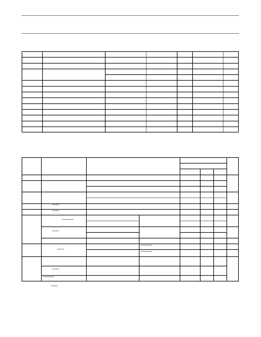
TIMING REQUIREMENTS--PC1600-PC2700
Over recommended operating conditions; T
amb
= 0 to +70
∞
C (unless otherwise noted) (see Figure 1)
LIMITS
SYMBOL
PARAMETER
TEST CONDITIONS
V
CC
= 2.5 V
±
0.2 V
UNIT
MIN
MAX
f
clock
Clock frequency
--
200
MHz
t
w
Pulse duration, CLK, CLK HIGH or LOW
1.0
--
ns
Data before CLK
, CLK
0.2
--
t
su
Setup time
RESET HIGH before CLK
, CLK
0.8
--
ns
t
h
Hold time
0.75
--
ns
TIMING REQUIREMENTS--PC3200
Over recommended operating conditions; T
amb
= 0 to +70
∞
C (unless otherwise noted) (see Figure 1)
LIMITS
SYMBOL
PARAMETER
TEST CONDITIONS
V
CC
= 2.5 V
±
0.2 V
UNIT
MIN
MAX
f
clock
Clock frequency
--
210
MHz
t
w
Pulse duration, CLK, CLK HIGH or LOW
1.0
--
ns
Data before CLK
, CLK
0.2
--
t
su
Setup time
RESET HIGH before CLK
, CLK
0.8
--
ns
t
h
Hold time
0.75
--
ns
Philips Semiconductors
Product data
SSTVF16857
DDR PC1600-PC3200 14-bit SSTL_2
registered driver with differential clock inputs
2003 Sep 19
7
SWITCHING CHARACTERISTICS--PC1600-PC2700
Over recommended operating conditions; T
amb
= 0 to +70
∞
C; V
DDQ
= 2.3 - 2.7 V and V
DDQ
does not exceed V
CC.
Class I, V
REF
= V
TT
= V
DDQ
◊
0.5 and C
L
= 10 pF (unless otherwise noted) (see Figure 1)
LIMITS
SYMBOL
FROM
TO
V
CC
= 2.5 V
±
0.2 V
UNIT
(INPUT)
(OUTPUT)
MIN
MAX
f
max
Maximum clock frequency
200
--
MHz
t
PLH
/t
PHL
CLK and CLK
Q
1.0
2.6
ns
t
PHL
RESET
Q
2.0
4.0
ns
SWITCHING CHARACTERISTICS--PC3200
Over recommended operating conditions; T
amb
= 0 to +70
∞
C; V
DDQ
= 2.3 - 2.7 V and V
DDQ
does not exceed V
CC.
Class I, V
REF
= V
TT
= V
DDQ
◊
0.5 and C
L
= 10 pF (unless otherwise noted) (see Figure 1)
LIMITS
SYMBOL
FROM
TO
V
CC
= 2.5 V
±
0.2 V
UNIT
(INPUT)
(OUTPUT)
MIN
MAX
f
max
Maximum clock frequency
210
--
MHz
t
PLH
/t
PHL
CLK and CLK
Q
1.0
2.6
ns
t
PHL
RESET
Q
2.0
4.0
ns
Philips Semiconductors
Product data
SSTVF16857
DDR PC1600-PC3200 14-bit SSTL_2
registered driver with differential clock inputs
2003 Sep 19
8
PARAMETER MEASUREMENT INFORMATION
AC WAVEFORMS
V
OL
t
PLH
t
PHL
OUTPUT
V
REF
V
REF
V
REF
V
IH
V
IL
CLK
V
OH
V
REF
SW00836
Waveform 1. Propagation delay times
V
REF
V
REF
V
IH
V
IL
OUTPUT
t
PHL
SW00837
V
OH
V
OL
RESET
Waveform 2. Propagation delay RESET to output.
V
REF
V
REF
V
IH
V
IL
INPUT
SW00339
t
W
Waveform 3. Pulse duration
V
REF
V
IH
V
IL
TIMING INPUT
SW00340
V
REF
V
REF
V
IL
DATA INPUT
t
h
t
su
V
IH
Waveform 4. Setup and hold times
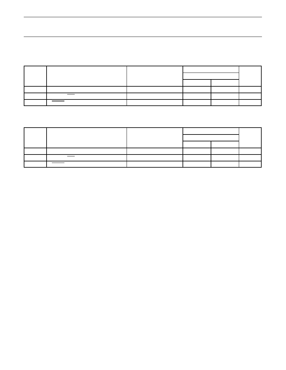
TEST CIRCUIT
V
TT
TEST POINT
C
L
= 30 pF
50
NOTES:
C
L
includes probe and jig capacitance
All input pulses are supplied by generators having the following characteristics:
PRR
10 MHz, Z
O
= 50
, t
r
1.25 ns/V, t
f
1.25 ns/V.
The outputs are measured one at a time with one transition per measurement.
V
TT
= V
REF
= V
DDQ
x 0.5
SW00838
Figure 1. Load circuitry
Philips Semiconductors
Product data
SSTVF16857
DDR PC1600-PC3200 14-bit SSTL_2
registered driver with differential clock inputs
2003 Sep 19
9
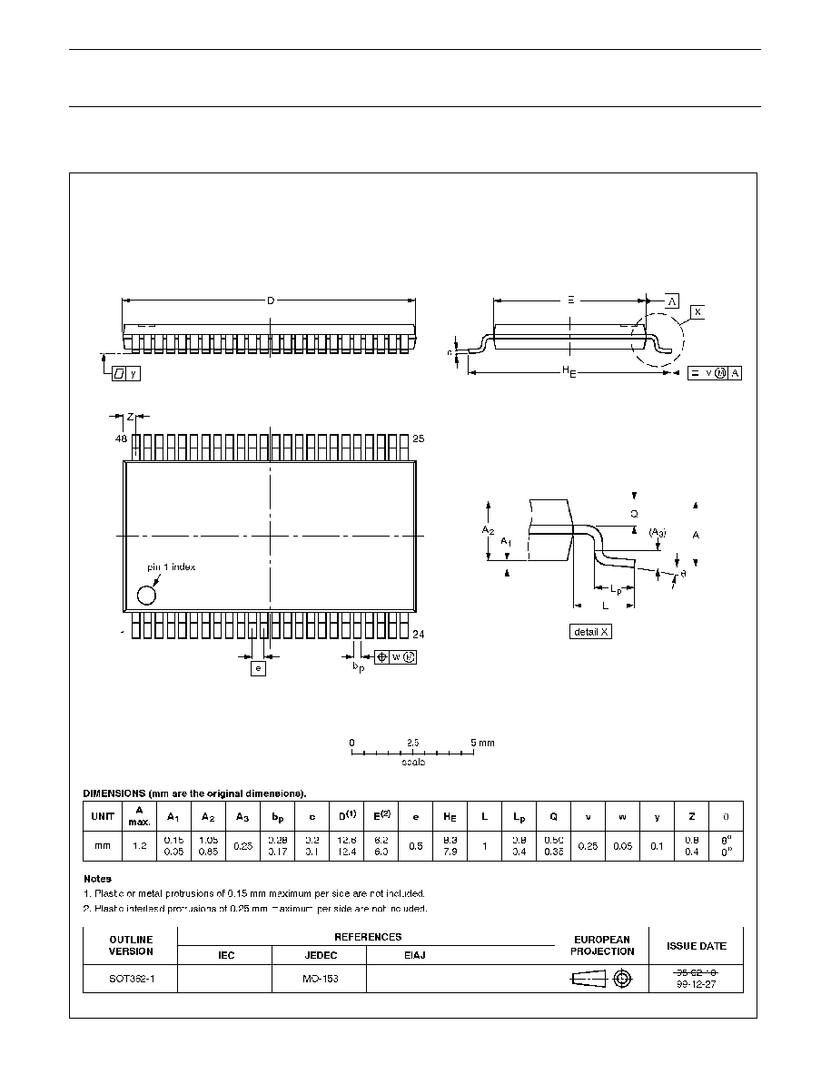
TSSOP48:
plastic thin shrink small outline package; 48 leads; body width 6.1 mm
SOT362-1
Philips Semiconductors
Product data
SSTVF16857
DDR PC1600-PC3200 14-bit SSTL_2
registered driver with differential clock inputs
2003 Sep 19
10
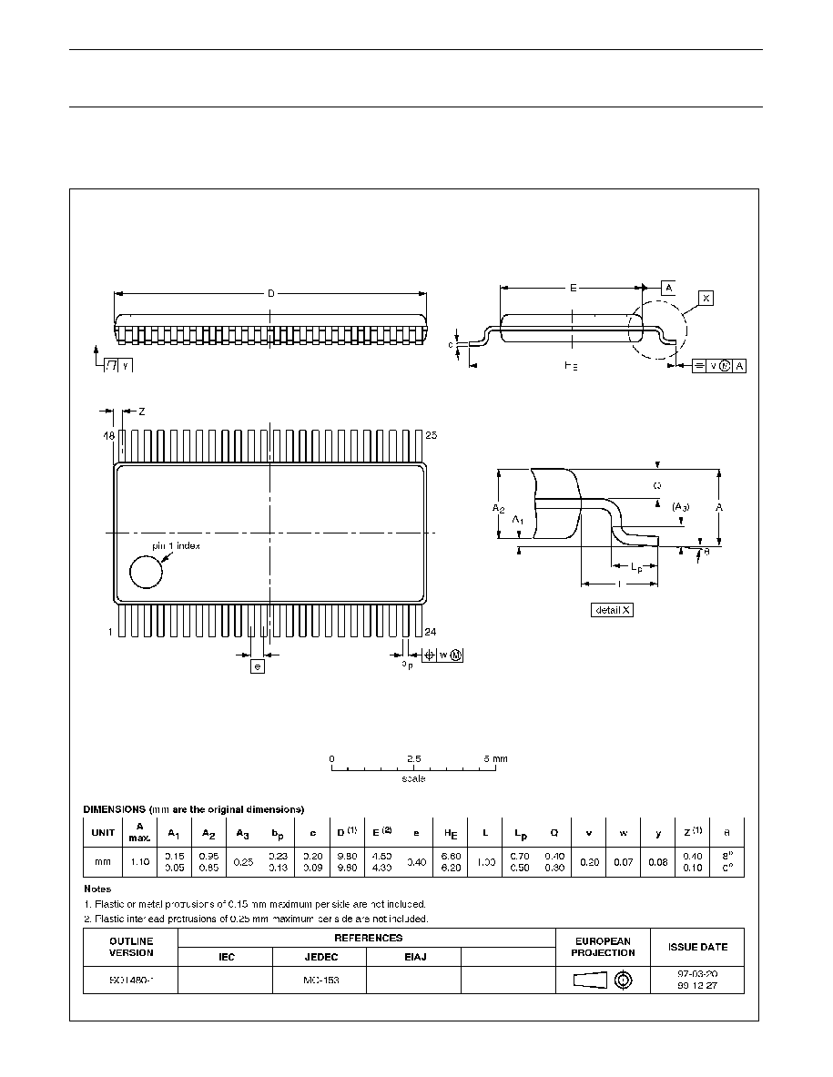
TSSOP48:
plastic thin shrink small outline package; 48 leads;
body width 4.4 mm; lead pitch 0.4 mm
SOT480-1
Philips Semiconductors
Product data
SSTVF16857
DDR PC1600-PC3200 14-bit SSTL_2
registered driver with differential clock inputs
2003 Sep 19
11
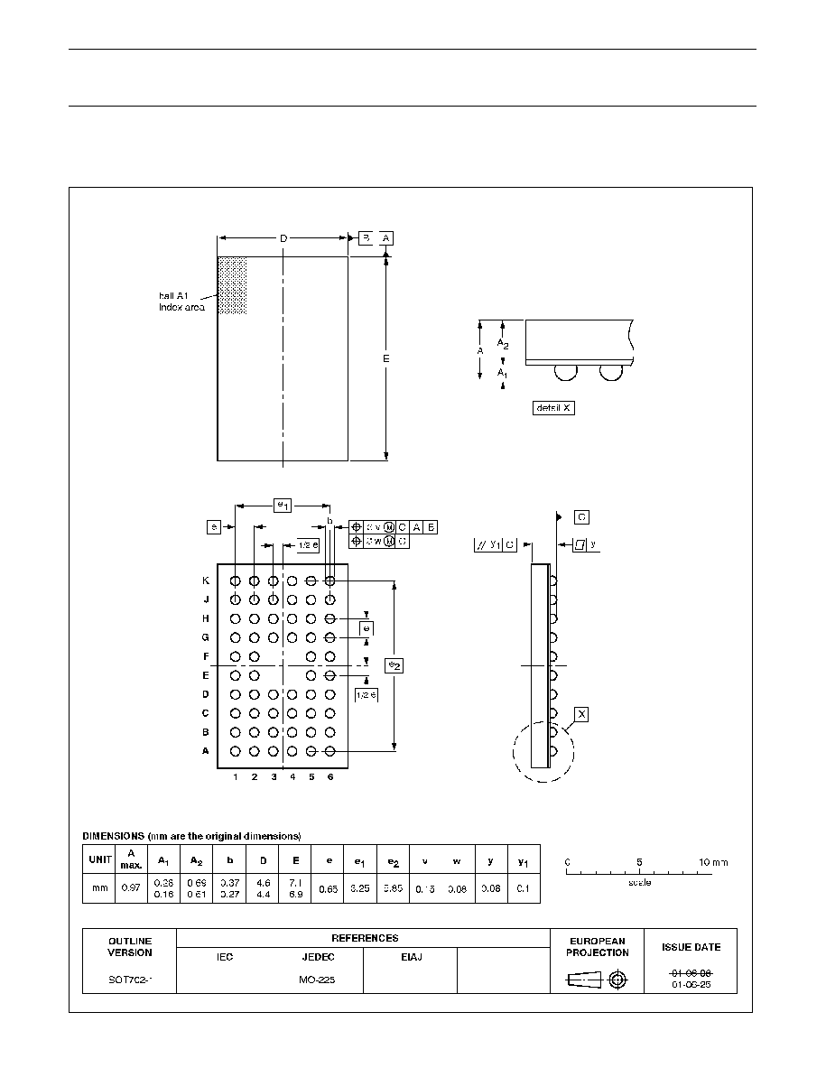
VFBGA56:
plastic very thin fine-pitch ball grid array package; 56 balls;
body 4.5 x 7 x 0.65 mm
SOT702-1

Philips Semiconductors
Product data
SSTVF16857
DDR PC1600-PC3200 14-bit SSTL_2
registered driver with differential clock inputs
2003 Sep 19
12
REVISION HISTORY
Rev
Date
Description
_1
20030919
Product data (9397 750 12077); ECN 853-2405 30362
dated 18 September 2003.
Philips Semiconductors
Product data
SSTVF16857
DDR PC1600-PC3200 14-bit SSTL_2
registered driver with differential clock inputs
2003 Sep 19
13
Definitions
Short-form specification -- The data in a short-form specification is extracted from a full data sheet with the same type number and title. For detailed information see
the relevant data sheet or data handbook.
Limiting values definition -- Limiting values given are in accordance with the Absolute Maximum Rating System (IEC 60134). Stress above one or more of the limiting
values may cause permanent damage to the device. These are stress ratings only and operation of the device at these or at any other conditions above those given
in the Characteristics sections of the specification is not implied. Exposure to limiting values for extended periods may affect device reliability.
Application information -- Applications that are described herein for any of these products are for illustrative purposes only. Philips Semiconductors make no
representation or warranty that such applications will be suitable for the specified use without further testing or modification.
Disclaimers
Life support -- These products are not designed for use in life support appliances, devices, or systems where malfunction of these products can reasonably be
expected to result in personal injury. Philips Semiconductors customers using or selling these products for use in such applications do so at their own risk and agree
to fully indemnify Philips Semiconductors for any damages resulting from such application.
Right to make changes -- Philips Semiconductors reserves the right to make changes in the products--including circuits, standard cells, and/or software--described
or contained herein in order to improve design and/or performance. When the product is in full production (status `Production'), relevant changes will be communicated
via a Customer Product/Process Change Notification (CPCN). Philips Semiconductors assumes no responsibility or liability for the use of any of these products, conveys
no license or title under any patent, copyright, or mask work right to these products, and makes no representations or warranties that these products are free from patent,
copyright, or mask work right infringement, unless otherwise specified.
Contact information
For additional information please visit
http://www.semiconductors.philips.com.
Fax: +31 40 27 24825
For sales offices addresses send e-mail to:
sales.addresses@www.semiconductors.philips.com.
Koninklijke Philips Electronics N.V. 2003
All rights reserved. Printed in U.S.A.
Date of release: 09-03
Document order number:
9397 750 12077
Philips
Semiconductors
Data sheet status
[1]
Objective data
Preliminary data
Product data
Product
status
[2] [3]
Development
Qualification
Production
Definitions
This data sheet contains data from the objective specification for product development.
Philips Semiconductors reserves the right to change the specification in any manner without notice.
This data sheet contains data from the preliminary specification. Supplementary data will be published
at a later date. Philips Semiconductors reserves the right to change the specification without notice, in
order to improve the design and supply the best possible product.
This data sheet contains data from the product specification. Philips Semiconductors reserves the
right to make changes at any time in order to improve the design, manufacturing and supply. Relevant
changes will be communicated via a Customer Product/Process Change Notification (CPCN).
Data sheet status
[1] Please consult the most recently issued data sheet before initiating or completing a design.
[2] The product status of the device(s) described in this data sheet may have changed since this data sheet was published. The latest information is available on the Internet at URL
http://www.semiconductors.philips.com.
[3] For data sheets describing multiple type numbers, the highest-level product status determines the data sheet status.
Level
I
II
III