 | –≠–ª–µ–∫—Ç—Ä–æ–Ω–Ω—ã–π –∫–æ–º–ø–æ–Ω–µ–Ω—Ç: SZF2002 | –°–∫–∞—á–∞—Ç—å:  PDF PDF  ZIP ZIP |
DATA SHEET
Product specification
File under Integrated Circuits, IC20
1998 Aug 26
INTEGRATED CIRCUITS
SZF2002
Low voltage 8-bit microcontroller
with 6-kbyte embedded RAM

1998 Aug 26
2
Philips Semiconductors
Product specification
Low voltage 8-bit microcontroller with
6-kbyte embedded RAM
SZF2002
CONTENTS
1
FEATURES
2
GENERAL DESCRIPTION
3
APPLICATIONS
4
ORDERING INFORMATION
5
BLOCK DIAGRAM
6
FUNCTIONAL DIAGRAM
7
PINNING INFORMATION
7.1
Pinning
7.2
Pin description
8
FUNCTIONAL DESCRIPTION
8.1
General
8.2
CPU timing
9
MEMORY ORGANIZATION
9.1
Program memory
9.2
Data memory
9.3
Special Function Registers (SFRs)
9.4
Addressing
9.5
Paging logic
10
PROGRAM STATUS WORD (PSW)
11
I/O FACILITIES
11.1
Ports
11.2
Port configuration
12
TIMER/EVENT COUNTERS
12.1
Timer 0 and Timer 1
12.2
Timer 2
12.3
Timer/Counter 2 Control Register (T2CON)
12.4
Timer/Counter 2 Mode Register (T2MOD)
12.5
Watchdog Timer (T3)
13
PULSE WIDTH MODULATED OUTPUT
13.1
Prescaler Frequency Control Register (PWMP)
13.2
Pulse Width Register (PWM)
14
ANALOG-TO-DIGITAL CONVERTER (ADC)
14.1
ADC Control Register (ADCON)
14.2
ADC Result Register (ADCH)
15
REDUCED POWER MODES
15.1
Idle mode
15.2
Power-down mode
15.3
Wake-up from Power-down mode
15.4
Status of external pins
15.5
Power Control Register (PCON)
16
I
2
C-BUS SERIAL I/O
16.1
Serial Control Register (S1CON)
16.2
Serial Status Register (S1STA)
16.3
Data Shift Register (S1DAT)
16.4
Address Register (S1ADR)
17
STANDARD SERIAL INTERFACE SIO0:
UART
17.1
Multiprocessor communications
17.2
Serial Port Control and Status Register
(S0CON)
17.3
Baud rates
18
INTERRUPT SYSTEM
18.1
External interrupts INT2 to INT8
18.2
Interrupt priority
18.3
Interrupt related registers
19
CLOCK CIRCUITRY
20
RESET
20.1
External reset using the RST pin
20.2
Power-on-reset
21
SPECIAL FUNCTION REGISTERS
OVERVIEW
22
DEBUGGING SUPPORT
22.1
Recommended equipment
22.2
Connecting the pod
22.3
Powering the pod
22.4
Bank switching support
22.5
Software recommendations
23
INSTRUCTION SET
24
LIMITING VALUES
25
DC CHARACTERISTICS
26
ADC CHARACTERISTICS
27
AC CHARACTERISTICS
28
PACKAGE OUTLINE
29
SOLDERING
29.1
Introduction
29.2
Reflow soldering
29.3
Wave soldering
29.4
Repairing soldered joints
30
DEFINITIONS
31
LIFE SUPPORT APPLICATIONS
32
PURCHASE OF PHILIPS I
2
C COMPONENTS

1998 Aug 26
3
Philips Semiconductors
Product specification
Low voltage 8-bit microcontroller with
6-kbyte embedded RAM
SZF2002
1
FEATURES
∑
Fully static 80C51 Central Processing Unit (CPU)
∑
8-bit CPU, ROM, RAM and I/O in a 80 lead LQFP
package
∑
6-kbytes ROM program memory, expandable externally
to 256 kbytes
∑
6144 + 256 bytes low power RAM data memory,
expandable externally to 32 kbytes
∑
Internal AUX RAM can be used for program execution
(only in combination with internal ROM)
∑
Three 8-bit ports; 24 I/O lines
∑
Three 16-bit timer/event counters
∑
Flash Memory Interface optimized, with power saving
and programming options
∑
Internal demultiplexing and latching of address/data bus
to reduce system component count
∑
Interfaces to up to 256-kbyte Flash Memory (banked)
∑
Fifteen source, fifteen vector nested interrupt structure
with two priority levels
∑
Full duplex serial port (UART)
∑
I
2
C-bus interface for serial transfer on two lines
∑
Analog-to-Digital Converter (ADC) with Power-down
mode; 6 input channels and 8-bit ADC
∑
Pulse Width Modulated (PWM) output (8-bit resolution)
∑
Watchdog Timer
∑
Enhanced architecture with:
≠ Non-page oriented instructions
≠ Direct addressing
≠ Four 8-byte RAM register banks
≠ Stack depth limited only by available internal RAM
(maximum 256 bytes)
≠ Multiply, divide, subtract and compare instructions
∑
Modes of reduced activity: Power-down and Idle modes
∑
Wake-up via external interrupts at INT0 to INT8
∑
Frequency range: up to 16 MHz (only limited by external
memory and ADC performance)
∑
Supply voltage: 3.0 V
∑
Very low power consumption:
operational 0.65 mW/MHz; Idle 0.25 mW/MHz at 3.0 V
∑
Operating temperature:
-
40 to +85
∞
C.
2
GENERAL DESCRIPTION
The SZF2002 low power system controller is
manufactured in an advanced 0.5
µ
m CMOS technology.
The instruction set of the SZF2002 is based on that of the
80C51 and consists of over 100 instructions: 49 one-byte,
46 two-byte, and 16 three-byte. The device has low power
consumption and two software selectable modes for
power reduction: Idle and Power-down.
This data sheet details the specific properties of the
SZF2002; for details of the 80C51 core and peripheral
functions such as timers, UART and I/O, see
"Data Handbook IC20". For the I
2
C-bus refer to
"The
I
2
C-bus and how to use it", ordering number
9398 393 40011.
3
APPLICATIONS
The SZF2002 is an 8-bit general purpose microcontroller
especially suited for wireless telephone and battery
powered applications. The SZF2002 also functions as an
arithmetic processor having facilities for both binary and
BCD arithmetic plus bit-handling capabilities.
4
ORDERING INFORMATION
TYPE
NUMBER
PACKAGE
NAME
DESCRIPTION
VERSION
SZF2002HL
LQFP80
plastic low profile quad flat package; 80 leads; body 12
◊
12
◊
1.4 mm
SOT315-1
1998 Aug 26
4
Philips Semiconductors
Product specification
Low voltage 8-bit microcontroller with
6-kbyte embedded RAM
SZF2002
5
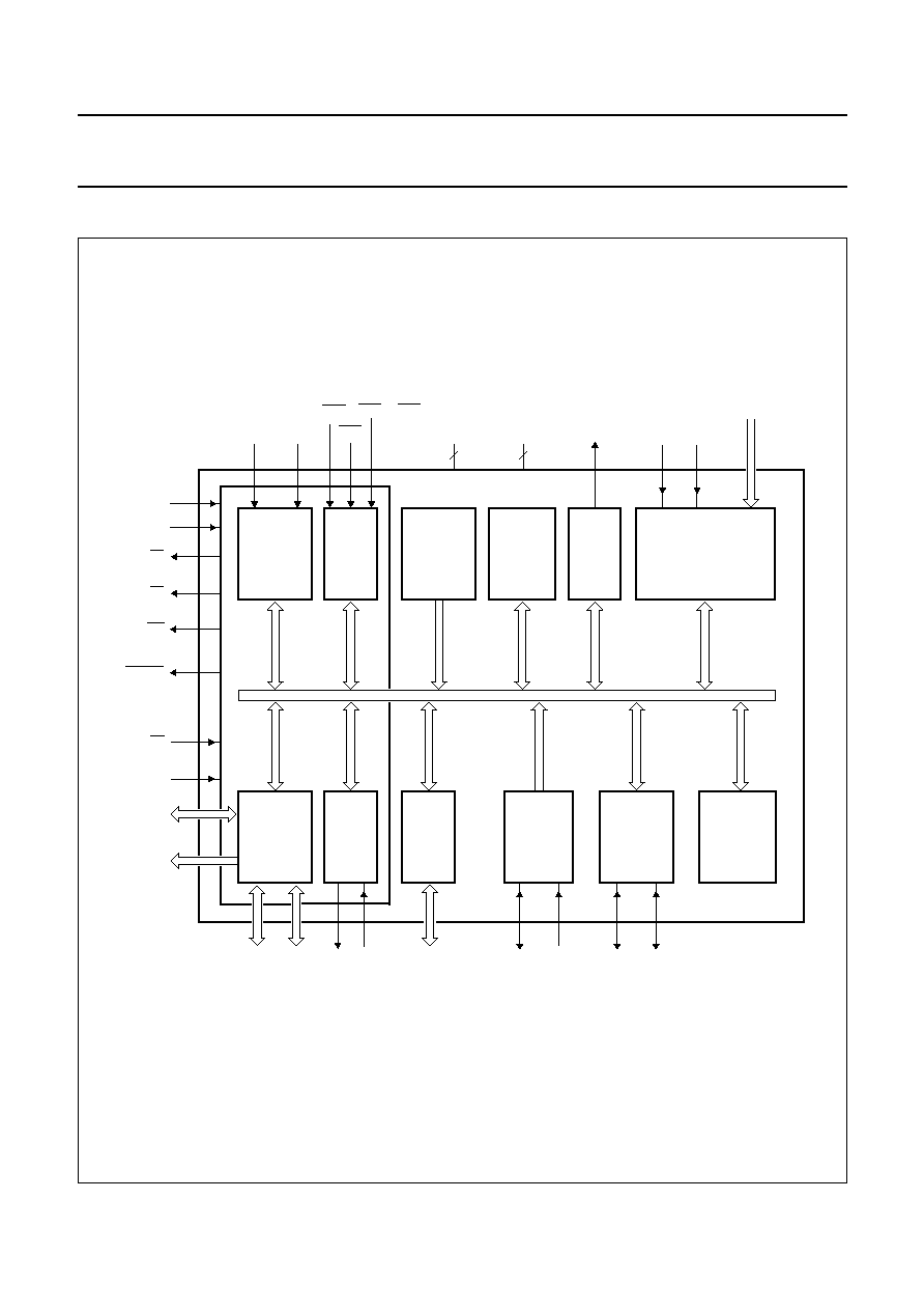
BLOCK DIAGRAM
Fig.1 Block diagram.
MGM180
RAMCE
RST
XCLK
D0 to D7
A0 to A17
CE
OE
WE
VSS
VDDA VSSA
VDD
RXD
TXD
P3
P1
T0
T1
INT0
INT1
PARALLEL
I/O PORTS
AND
EXT. BUS
SERIAL
UART
PORT
TWO 16-BIT
TIMER/
EVENT
COUNTERS
(T0, T1)
80C51
core
excluding
ROM/RAM
CPU
P4
8-BIT
I/O
PORTS
WATCHDOG
TIMER
(T3)
PROGRAM
MEMORY
DATA
MEMORY
PWM
ADC
ADC0 to ADC5
6-KBYTE
ROM
PWM
6144
+
256
bytes RAM
DEBUG
EA
SZF2002
T2EX
T2
16-BIT
TIMER/
EVENT
COUNTER
SDA
SCL
I
2
C-BUS
INTERFACE
INT2 to INT8
3
3
(1) Address lines A0 to A5 have alternative functions during Debug; see Section 7.2.
1998 Aug 26
5
Philips Semiconductors
Product specification
Low voltage 8-bit microcontroller with
6-kbyte embedded RAM
SZF2002
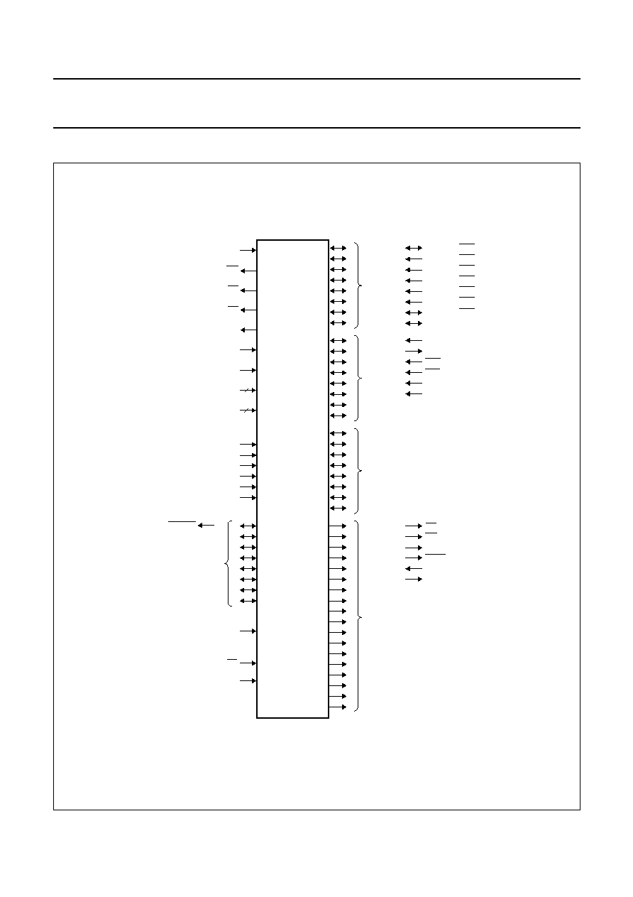
6
FUNCTIONAL DIAGRAM
Fig.2 Functional diagram.
handbook, full pagewidth
MGM181
PORT 1
0
0
0
0
0
PORT 3
address bus
data bus
PORT 4
RST
EA
DEBUG
ADC0
ADC1
ADC2
ADC3
ADC4
ADC5
VSS
VDD
VDDA
RST
TRUE_A15
RD
WR
PSEN
ALE
RXD
TXD
T0
T1
INT1
INT0
SZF2002
PWM
CE
RAMCE
OE
WE
XCLK
VSSA
T2
INT2
T2EX INT3
INT5
INT4
INT6
SCL
SDA
INT8
INT7
3
3
1998 Aug 26
6
Philips Semiconductors
Product specification
Low voltage 8-bit microcontroller with
6-kbyte embedded RAM
SZF2002
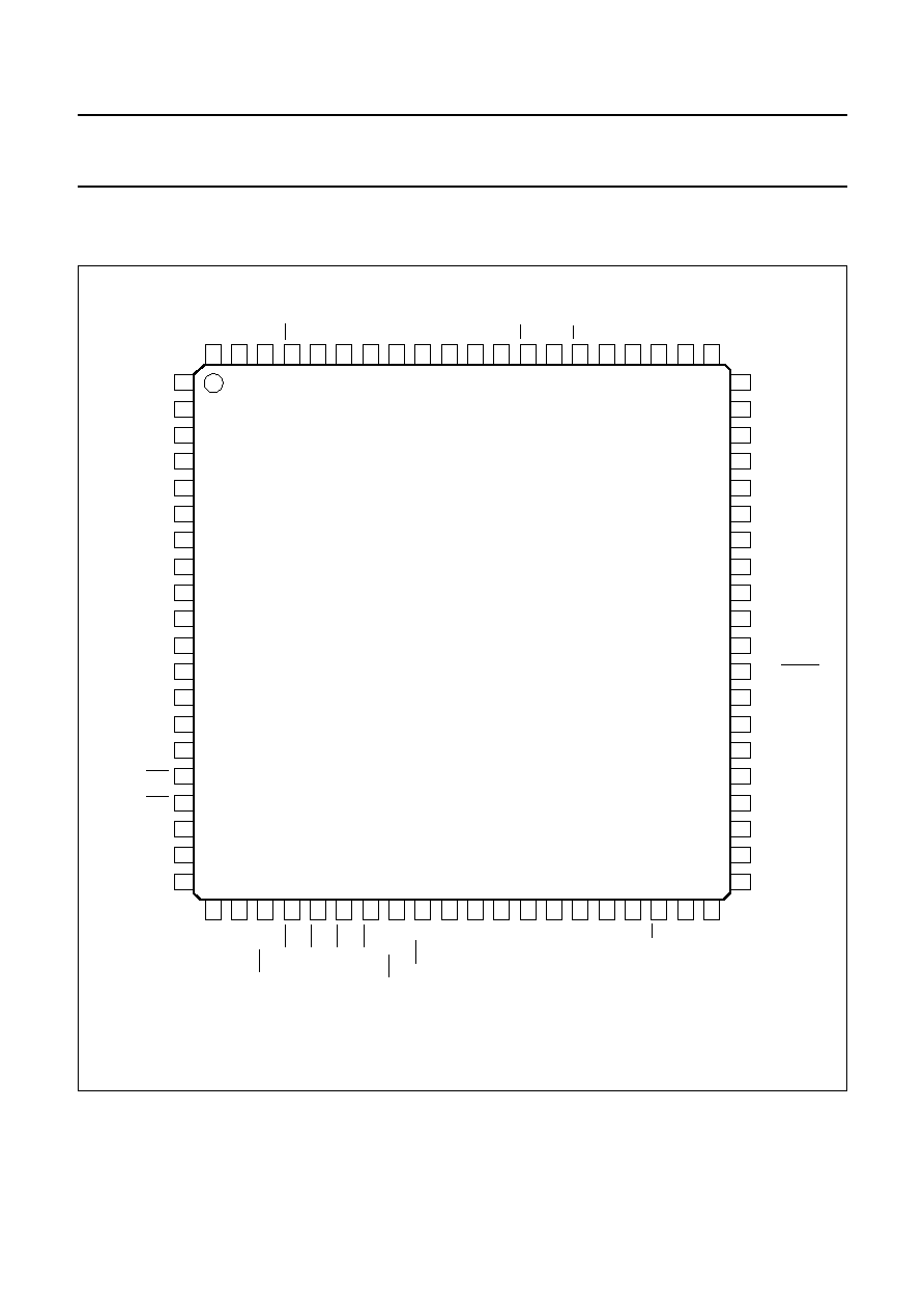
7
PINNING INFORMATION
7.1
Pinning
Fig.3 Pin configuration.
P1.6/INT8/SCL
handbook, full pagewidth
SZF2002
MGM182
1
2
3
4
5
6
7
8
9
10
11
12
13
14
15
16
17
18
19
n.c.
A12
A7
A6
A5
A4
PWM
RST
XCLK
VDD
VSS
P3.7
P3.6
P3.5/T1
P3.4/T0
P3.3/INT1
P3.2/INT0
P3.1/TXD
P3.0/RXD
n.c. 20
60
59
58
57
56
55
54
53
52
51
50
49
48
47
46
45
44
43
42
41
21
22
23
24
25
26
27
28
29
30
31
32
33
34
35
36
37
38
39
40
80
79
78
77
76
75
74
73
72
71
70
69
68
67
66
65
64
63
62
61
n.c.
A15
A16
WE
A17
A14
A13
A8
A9
V
SS
V
DD
A11
OE
A10
CE
D7
D6
D5
D4
n.c.
n.c.
P1.7/SDA
P1.5/INT7
P1.4/INT6
P1.3/INT5
P1.2/INT4
P1.1/INT3/T2EX
P1.0/INT2/T2
V
DDA
V
SSA
ADC5
ADC4
ADC3
ADC2
ADC1
ADC0
EA
DEBUG
n.c.
n.c.
D3
D2
D1
D0
A0
A1
A2
A3
VSS
VDD
P4.0/RAMCE
P4.1
P4.2
P4.3
P4.4
P4.5
P4.6
P4.7
n.c.
1998 Aug 26
7
Philips Semiconductors
Product specification
Low voltage 8-bit microcontroller with
6-kbyte embedded RAM
SZF2002
7.2
Pin description
Table 1
LQFP80 package
SYMBOL
PIN
DESCRIPTION
Program memory interface; note 1
A0
55
A0/RD. Address line 0, used as RD during Debug.
A1
54
A1/WR. Address line 1, used as WR during Debug.
A2
53
A2/ALE. Address line 2, used as ALE during Debug.
A3
52
A3/PSEN. Address line 3, used as PSEN during Debug.
A4
6
A4/RST. Address line 4, used as RST during Debug.
A5
5
A5/TRUE_A15. Address line 5, used as A15 = P2.7 during Debug.
A6
4
A6. Address line 6 (not needed during Debug, see D6).
A7
3
A7. Address line 7 (not needed during Debug, see D7).
A8
73
Address lines A8 to A14. During Debug these lines are used as P2.0 to P2.6.
A9
72
A10
67
A11
69
A12
2
A13
74
A14
75
A15
79
Address lines A15 to A17. Page selection; during Debug these lines are the page
register. Each bank is 32 kbytes.
A16
78
A17
76
D0
56
Data bus. During Debug these line are P0.0 to P0.7.
D1
57
D2
58
D3
59
D4
62
D5
63
D6
64
D7
65
CE
66
Chip Enable. Enable strobe to external program memory.
OE
68
Output Enable. Output read strobe to external memory.
WE
77
Write Enable. Write strobe to external memory.
1998 Aug 26
8
Philips Semiconductors
Product specification
Low voltage 8-bit microcontroller with
6-kbyte embedded RAM
SZF2002
I/O Ports
P1.0/INT2/T2
29
Port 1 (P1.0 to P1.7). 8-bit bidirectional I/O port with internal pull-ups; INT2 to INT8:
external interrupt inputs; T2: Timer T2 I/O; T2EX: Timer 2 external input; SCL:
I
2
C-bus interface clock; SDA: I
2
C-bus interface data.
Port 1 pins that have logic 1s written to them are pulled HIGH by the internal pull-ups,
and in that state can be used as inputs (note P1.6 and P1.7 are open-drain only).
As inputs, Port 1 pins that are externally pulled LOW will source current
(I
IL
, see Chapter 25) due to the internal pull-ups.
P1.1/INT3/T2EX
28
P1.2/INT4
27
P1.3/INT5
26
P1.4/INT6
25
P1.5/INT7
24
P1.6/INT8/SCL
23
P1.7/SDA
22
P3.0/RXD
19
Port 3 (P3.0 to P3.7). 8-bit bidirectional I/O port with internal pull-ups; RXD: serial
port receiver data input (asynchronous); TXD: serial port transmitter data output
(asynchronous); INT0: external interrupt 0; INT1: external interrupt 1;
T0: Timer 0 external input; T1: Timer 1 external input.
Port 3 pins that have logic 1s written to them are pulled HIGH by the internal pull-ups,
and in that state can be used as inputs. As inputs, Port 3 pins that are externally pulled
LOW will source current (I
IL
, see Chapter 25) due to the internal pull-ups.
P3.1/TXD
18
P3.2/INT0
17
P3.3/INT1
16
P3.4/T0
15
P3.5/T1
14
P3.6
13
P3.7
12
P4.0/RAMCE
49
Port 4 (P4.0 to P4.7). 8-bit bidirectional I/O port; RAMCE chip enable for external
RAM.
Port 4 pins that have logic 1s written to them are pulled HIGH by the internal pull-ups,
and in that state can be used as inputs. As inputs, Port 4 pins that are externally pulled
LOW will source current (I
IL
, see Chapter 25) due to the internal pull-ups.
P4.1
48
P4.2
47
P4.3
46
P4.4
45
P4.5
44
P4.6
43
P4.7
42
ADC interface
ADC0
37
Input channels to the ADC.
ADC1
36
ADC2
35
ADC3
34
ADC4
33
ADC5
32
SYMBOL
PIN
DESCRIPTION
1998 Aug 26
9
Philips Semiconductors
Product specification
Low voltage 8-bit microcontroller with
6-kbyte embedded RAM
SZF2002
Note
1. The pin layout has been optimized for easy connection of 256 kbytes Flash ROM (e.g. ATMEL AT29LV010A,
SGS-Thomson M28V201, or AMD Am29F010).
General
PWM
7
Pulse Width Modulation output.
RST
8
Reset. A HIGH level on this pin for at least 12 clock cycles resets the device.
XCLK
9
Clock input.
EA
38
External Access. When EA is HIGH the CPU executes out of internal program
memory (unless the program counter exceeds 7FFFH). A LOW EA forces the CPU to
execute out of external memory regardless of the value of the Program Counter. This
signal is latched at the falling edge of reset (RST pin). The EA pin has an internal
pull-down. When it is not connected the CPU executes from external memory.
DEBUG
39
DEBUG enable. If HIGH, forces standard 80C51 timing signals output at address and
databus. In this mode the databus is multiplexed with the lower 8 bits of the address
bus, and the A0 to A3 lines are used for the RD, WR, ALE and PSEN signals. This
allows a standard 80C51 in-circuit emulator to be connected. For normal operation
connect DEBUG to V
SS
.
Power
V
DD
10, 50,
70
Power supply digital core and digital I/O pads.
V
SS
11, 51,
71
Ground: circuit ground potential.
V
DDA
30
Analog power.
V
SSA
31
Analog ground.
n.c.
1, 20,
21, 40,
41, 60,
61, 80
Not connected.
SYMBOL
PIN
DESCRIPTION

1998 Aug 26
10
Philips Semiconductors
Product specification
Low voltage 8-bit microcontroller with
6-kbyte embedded RAM
SZF2002
8
FUNCTIONAL DESCRIPTION
Detailed descriptions of each function are described in:
Chapter 9 "Memory organization"
Chapter 10 "Program Status Word (PSW)"
Chapter 11 "I/O facilities"
Chapter 12 "Timer/event counters"
Chapter 13 "Pulse Width Modulated output"
Chapter 14 "Analog-to-digital converter (ADC)"
Chapter 15 "Reduced power modes"
Chapter 16 "I2C-bus serial I/O"
Chapter 17 "Standard serial interface SIO0: UART"
Chapter 18 "Interrupt system"
Chapter 19 "Clock circuitry"
Chapter 20 "Reset"
Chapter 21 "Special Function Registers overview"
Chapter 22 "Debugging support".
8.1
General
The SZF2002 is a stand-alone high-performance CMOS
microcontroller designed for use in real-time applications
such as wireless telephone and mobile communications,
instrumentation, industrial control, intelligent computer
peripherals and consumer products.
The device provides hardware features, architectural
enhancements and new instructions to function as a
controller for applications requiring up to 256 kbytes of
program memory and/or up to 6144 + 256 bytes of on-chip
data memory.
The SZF2002 contains a 6-kbyte program memory; a
static 6144 + 256 byte data memory (RAM); 24 I/O lines;
three 16-bit timer/event counters; a fifteen-source two
priority-level, nested interrupt structure, a 6-channel 8-bit
ADC, a Watchdog Timer and a Pulse Width Modulation
output.
Two serial interfaces are provided on-chip:
∑
A standard UART serial interface
∑
A standard I
2
C-bus serial interface with a transfer speed
of up to 400 kbits/s (depending on clock frequency).
The I
2
C-bus serial interface has byte oriented master
and slave functions allowing communication with the
whole family of I
2
C-bus compatible devices.
The device has two software selectable modes of reduced
activity for power reduction:
∑
Idle mode: freezes the CPU while allowing the
derivative functions (timers, serial I/O, RAM,
ADC and PWM) and interrupt system to continue
functioning
∑
Power-down mode: saves the RAM contents but stops
the clock causing all other chip functions to be
inoperative.
8.2
CPU timing
A machine cycle consists of a sequence of 6 states. Each
state lasts one clock period, thus a machine cycle takes
6 clock periods or 1
µ
s if the clock frequency (f
clk
) is
6 MHz.

1998 Aug 26
11
Philips Semiconductors
Product specification
Low voltage 8-bit microcontroller with
6-kbyte embedded RAM
SZF2002
9
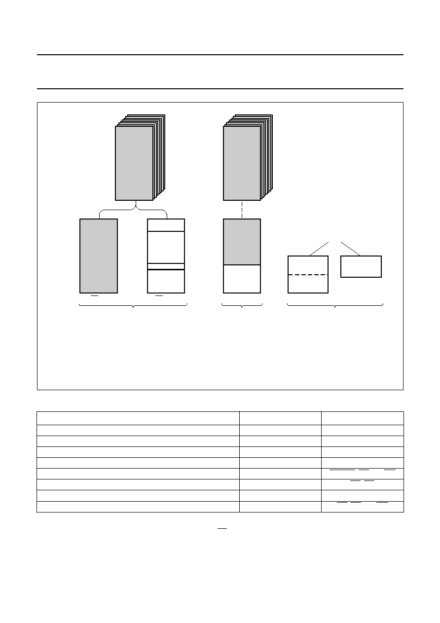
MEMORY ORGANIZATION
The SZF2002 has 6 kbytes of program memory plus
6 kbytes + 256 bytes of data memory on chip. The device
has separate address spaces for program and data
memory (see Fig.4).
The SZF2002 can directly address up to 256 kbytes of
external data memory. The CPU generates the read
strobe (OE), the write strobe (WE) and chip select (CE) for
external program memory (Flash), and read strobe (OE)
and write strobe (WE) and chip select (RAMCE) for
external data memory.
9.1
Program memory
The SZF2002 contains 6 kbytes of internal ROM and
6144 + 256 bytes of RAM. The lower 6 kbytes of program
memory can be implemented in either on-chip ROM or
external program memory. The 6 kbytes of program
memory is implemented as mask programmable ROM.
There are two modes for the program memory, depending
on the state of the EA pin (latched during reset) and on the
address range:
1. EA = 0. All program fetches are directed to the
external program memory. After reset the CPU begins
execution at location 8000H.
2. EA = 1. After reset the CPU begins execution at
location 0000H. Fetches from addresses
2000H to 37FFH are redirected to the Auxiliary RAM.
The processor can fill this RAM with normal write
operations to the data memory (MOVX to addresses
0000H to 17FFH). Program memory fetches from
addresses 0000H to 17FFH are directed to the
internal ROM.
Program Counter values greater than 7FFFH are
automatically addressed to external memory regardless of
the state of the EA pin.
9.2
Data memory
The SZF2002 contains 6144 + 256 bytes of RAM and a
number of Special Function Registers (SFRs). All these
data spaces are addressed differently. Figure 4 shows the
internal data memory space divided into the lower
128 bytes, the upper 128 bytes, Auxiliary RAM, and the
SFRs space. Internal RAM locations 0 to 127 are directly
and indirectly addressed. Internal RAM locations
128 to 255 are only indirectly addressed.
The Special Function Register locations 128 to 255 are
only directly addressed. Auxiliary RAM is accessible via
MOVX instructions to the lower 32-kbyte address space.
MOVX @R0/R1 instructions use SFR P2 as page
selector. The upper 32-kbyte address space is redirected
to the program memory, to accommodate flash
programming.
9.3
Special Function Registers (SFRs)
The upper 128 bytes are the address locations of the
SFRs. Figures 6 and 7 show the Special Function
Registers space. The SFRs include the port latches,
timers, peripheral control, serial I/O registers, etc. These
registers are accessed by direct addressing. There are
128 directly addressed locations in the SFR address
space. Bit addressed SFRs are those that end in 000B.
9.4
Addressing
The SZF2002 has five methods for addressing source
operands:
∑
Register
∑
Direct
∑
Indirect
∑
Immediate
∑
Base-Register plus Index-Register-Indirect.
The first three methods can be used for addressing
destination operands. Most instructions have a
`destination/source' field that specifies the data type,
addressing methods and operands involved.
For operations other than MOVs, the destination operand
is also a source operand.
Access to memory addressing is as follows:
∑
Registers in one of the four register banks through Direct
or Indirect (see Fig.5)
∑
Lower 128 bytes of internal RAM through Direct or
register Indirect; upper 128 bytes of internal RAM
through Indirect
∑
Special Function Registers through Direct
∑
Program memory look-up tables through Base-Register
plus Index-Register-Indirect
∑
Extended data memory access through register Indirect.
1998 Aug 26
12
Philips Semiconductors
Product specification
Low voltage 8-bit microcontroller with
6-kbyte embedded RAM
SZF2002
Table 2
Memory spaces; note 1
Notes
1. Execution from internal memory is only possible when EA = 1 during reset.
2. Page select is used to access all 8 banks in the 256-kbyte address space.
MEMORY SPACE
ADDRESS MODE
USED SIGNAL
Internal RAM 00H to 7FH
direct and indirect
-
Internal RAM 80H to FFH
indirect
-
SFRs 80H to FFH
direct
-
Internal AUX RAM (on-chip) 0000H to 17FFH
MOVX
-
External RAM (off-chip) 1800H to 7FFFH
MOVX
RAMCE, OE and WE
External ROM (off-chip) 0000H to FFFFH; note 2
program execution
CE, OE
Internal AUX RAM (on-chip) 2000H to 37FFH
program execution
-
External Flash ROM write (off-chip) 8000H to FFFFH; note 2
MOVX
CE, OE and WE
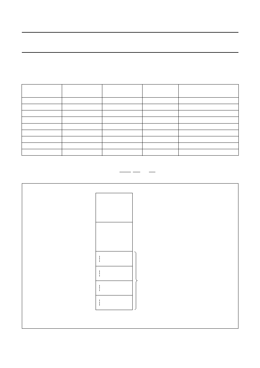
Fig.4 Memory map.
(1) Accessible via indirect addressing only.
(2) Accessible via direct and indirect addressing.
(3) Accessible via direct addressing.
(4) Gaps in the address map are undefined, and should not be used.
handbook, full pagewidth
MGM183
EXTERNAL
FLASH ROM
(BANKED)
FFFFH
8000H
EXTERNAL
ROM
BANK 0
7FFFH
0000H
EXTERNAL
RAM
INTERNAL
AUX RAM
(MOVX)
7FFFH
0000H
1800H
17FFH
INTERNAL
AUX RAM
6-KBYTE
INTERNAL
ROM
EA = 1
(4)
37FFH
0000H
2000H
17FFH
EXTERNAL
FLASH ROM
(BANKED)
FFFFH
8000H
overlapped space
INTERNAL
RAM
00H
FFH
80H
SPECIAL
FUNCTION
REGISTERS
EA = 0
(1)
(2)
(3)
INTERNAL MEMORY
DATA MEMORY
PROGRAM MEMORY
,,,
,,,
,,,
,,,
1998 Aug 26
13
Philips Semiconductors
Product specification
Low voltage 8-bit microcontroller with
6-kbyte embedded RAM
SZF2002
9.5
Paging logic
The SZF2002 contains paging logic to handle the extended address range.
Table 3
Paging of external memory; notes 1 and 2
Notes
1. During Debug A<17-15> are used to output the bank register. The TRUE_ A15 line is output at the A5 pin.
2. During Debug ROM and RAM access is done via PSEN, WR and RD.
TRUE_A15
(INTERNAL)
BANK SFR [2 : 0]
A<17-15> PINS
BANK
REMARK
0
XXX
000
0
lower 32 kbytes always bank 0
1
000
000
0
bank 0
1
001
001
1
bank 1
1
010
010
2
bank 2
1
011
011
3
bank 3
1
100
100
4
bank 4
1
101
101
5
bank 5
1
110
110
6
bank 6
1
111
111
7
bank 7
Fig.5 The lower 128 bytes of internal RAM.
handbook, halfpage
MGD675
R7
R0
07H
0
R7
R0
0FH
08H
R7
R0
17H
10H
R7
R0
1FH
18H
2FH
7FH
20H
30H
4 banks of 8 registers
(R0 to R7)
1998 Aug 26
14
Philips Semiconductors
Product specification
Low voltage 8-bit microcontroller with
6-kbyte embedded RAM
SZF2002
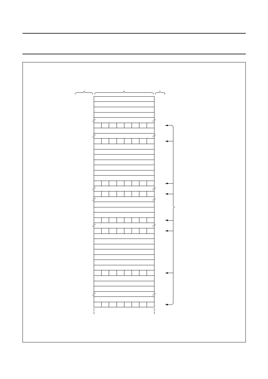
Fig.6 Special Function Register memory map.
MGM184
FE
FF
FD
FC
FB
FA
F9
F8
F6
F7
F5
F4
F3
F2
F1
F0
EE
EF
ED
EC
EB
EA
E9
E8
E6
E7
E5
E4
E3
E2
E1
E0
DE
DF
DD
DC DB
DA
D9
D8
D6
D7
D5
D4
D3
D2
D1
D0
CE
CF
CD CC
CB
CA C9
C8
C6
C7
C5
C4
C3
C2
C1
C0
BIT ADDRESS
REGISTER
MNEMONIC
FFH
T3
DIRECT
BYTE
ADDRESS (HEX)
FEH
FDH
FCH
PWMP
PWM
F8H
F7H
F0H
EFH
EEH
EDH
ECH
EBH
EAH
E8H
E0H
DBH
DAH
D9H
D8H
D0H
CFH
CEH
CDH
CCH
CBH
CAH
C9H
C8H
C5H
C4H
C0H
C1H
SFRs containing
directly addressable
bits
IP1
WDTKEY
B
IEN1
ACC
S1ADR
S1DAT
S1STA
S1CON
PSW
TH2
TL2
RCAP2H
RCAP2L
T2CON
T2MOD
ADCH
ADCON
P4
IRQ1
IX1
E9H
1998 Aug 26
15
Philips Semiconductors
Product specification
Low voltage 8-bit microcontroller with
6-kbyte embedded RAM
SZF2002
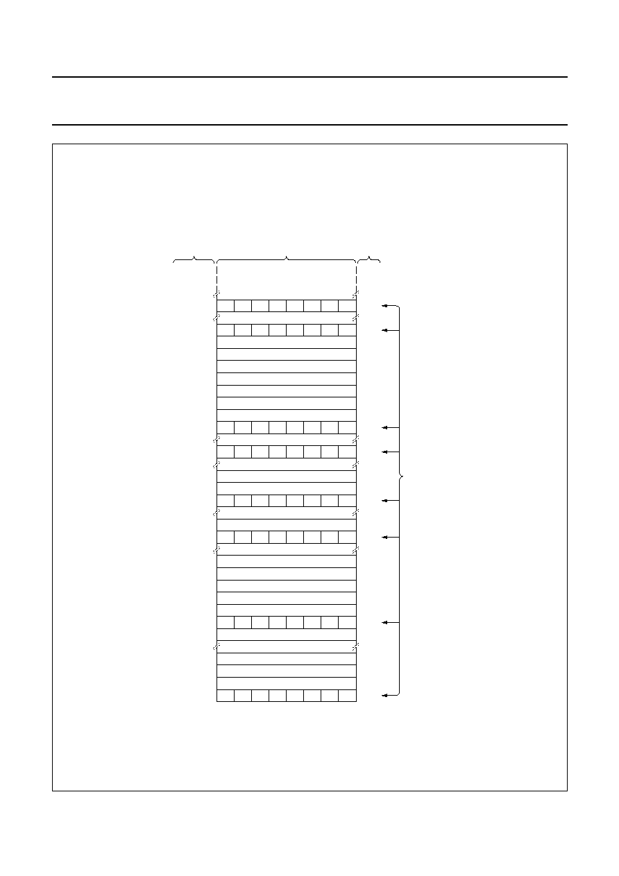
Fig.7 Special Function Register memory map (continued from Fig.6).
MGM185
BE
BD
BC
BB
BA
B9
B8
B6
B7
B5
B4
B3
B2
B1
B0
AE
AF
AD
AC
AB
AA
A9
A8
A6
A7
A5
A4
A3
A2
A1
A0
9E
9F
9D
9C
9B
9A
99
98
96
97
95
94
93
92
91
90
8E
8F
8D
8C
8B
8A
89
88
86
87
85
84
83
82
81
80
BIT ADDRESS
REGISTER
MNEMONIC
DIRECT
BYTE
ADDRESS
B8H
B0H
AFH
AEH
ADH
ACH
ABH
AAH
A8H
A0H
99H
9AH
98H
90H
91H
8DH
8CH
8BH
8AH
89H
88H
87H
83H
82H
81H
80H
SFRs containing
directly addressable
bits
IP0
P3
P2
(used as
address bus)
(used as
address bus)
S0BUF
S0CON
ROMBANK
P1
TH1
TH0
TL1
TL0
TMOD
PCON
DPH
DPL
SP
P0
IEN0
TCON
A9H
1998 Aug 26
16
Philips Semiconductors
Product specification
Low voltage 8-bit microcontroller with
6-kbyte embedded RAM
SZF2002
10 PROGRAM STATUS WORD (PSW)
The Program Status Word contains several status bits that
reflect the current state of the CPU. The PSW, shown in
Table 4, resides in the SFR memory space. It contains the
Carry bit, the Auxiliary Carry (for BCD operations), the two
register bank select bits, the Overflow flag, a Parity bit and
two user-definable status flags.
The Carry bit, other than serving the function of a Carry bit
in arithmetic operations, also serves as the Accumulator
for a number of boolean operations.
Bits RS0 and RS1 are used to select one of the four
register banks; see Table 5. A number of instructions refer
to these RAM locations as R0 through to R7. The selection
of which of the four register banks is being referred to is
made on the basis of the state of RS0 and RS1 at
execution time.
The Parity bit reflects the number of 1s in the Accumulator:
P = 1, if the Accumulator contains an odd number of 1s,
and P = 0, if the Accumulator contains an even number of
1s. Thus, the number of 1s in the Accumulator plus P is
always even. The bits F0 and USR are uncommitted and
may be used as general purpose status flags.
Table 4
Program Status Word (SFR address D0H)
Table 5
Description of PSW bits
7
6
5
4
3
2
1
0
CY
AC
F0
RS1
RS0
OV
USR
P
BIT
SYMBOL
DESCRIPTION
7
CY
Carry flag. The Carry flag receives carry out from bit 7 of ALU operands.
6
AC
Auxiliary Carry flag. The Auxiliary Carry flag receives carry out from bit 3 of addition
operands.
5
F0
General purpose status flag.
4
RS1
Register Bank Select 1. This bit selects Register Bank 1.
3
RS0
Register Bank Select 0. This bit selects Register Bank 0.
2
OV
Overflow flag. This flag is set by arithmetic operations.
1
USR
USR. This is a user-definable flag.
0
P
Parity. If the Accumulator contains an odd number of 1s this bit is set to a logic 1 by
hardware. Otherwise, the state of this bit is a logic 0.
1998 Aug 26
17
Philips Semiconductors
Product specification
Low voltage 8-bit microcontroller with
6-kbyte embedded RAM
SZF2002
11 I/O FACILITIES
11.1
Ports
The SZF2002 has 24 I/O lines: ports P1, P3 and P4 of
which ports P1 and P3 are bit addressed (P0 and P2 are
always used as address/data bus). Ports 0 to 4 have the
following alternative functions:
Port 0 Used internally.
Port 1 Used for a number of special functions:
∑
Provides the inputs for the external interrupts:
INT2 to INT8
∑
The I
2
C-bus interface: SCL and SDA
∑
Counter inputs: T2 and T2EX.
Port 2 Used internally.
Port 3 Pins can be configured individually to provide:
∑
External interrupt request inputs: INT1 and INT0
∑
Counter input: T1 and T0
∑
UART input and output: RXD and TXD.
Port 4 Provides chip select for external data memory:
RAMCE.
To enable a port pin alternative function, the port bit latch
in its SFR must contain a logic 1.
Each port consists of a latch (SFRs P0 to P4), an output
driver and input buffer. Ports 1, 3 and 4 have internal
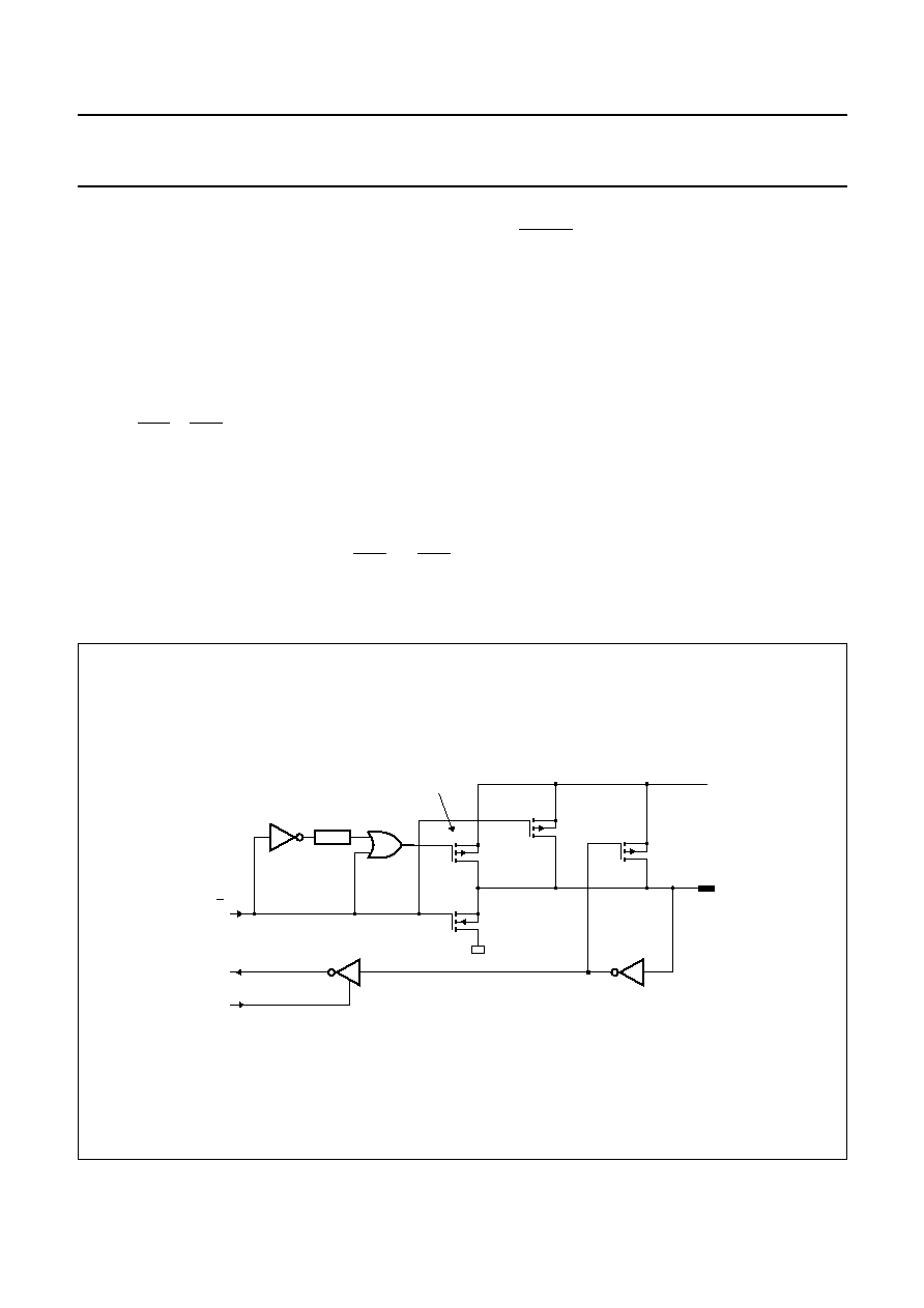
pull-ups (except P1.6 and P1.7). Figure 8 shows that the
strong transistor `p1' is turned on for only 2 clock periods
after a LOW-to-HIGH transition in the port latch. When on,
it turns on `p3' (a weak pull-up) through the inverter. This
inverter and `p3' form a latch which holds the logic 1.
In Port 0 the pull-up `p1' is only on when emitting logic 1s
for external memory access.
11.2
Port configuration
The port pins (except for P1.6 and P1.7) are configured as
shown in Fig.8. This is a quasi-bidirectional I/O with
pull-up. The strong booster pull-up `p1' is turned on for one
clock period after a LOW-to-HIGH transition in the port
latch. All port pins will be set to HIGH during reset.
Fig.8 Port configuration.
handbook, full pagewidth
MBK456
p1
p2
p3
input data
read port pin
2 clock
periods
n
strong pull-up
I/O pin
VDD
Q
from port latch
INPUT
BUFFER

1998 Aug 26
18
Philips Semiconductors
Product specification
Low voltage 8-bit microcontroller with
6-kbyte embedded RAM
SZF2002
12 TIMER/EVENT COUNTERS
The SZF2002 contains three 16-bit timer/event counter
registers; Timer 0, Timer 1 and Timer 2 which can perform
the following functions:
∑
Measure time intervals and pulse duration
∑
Count events
∑
Generate interrupt requests.
In the `Timer' operating mode the register increments
every machine cycle. Since a machine cycle consists of
6 clock periods, the count rate is
1
/
6
f
clk
.
In the `Counter' operating mode, the register increments in
response to a HIGH-to-LOW transition. Since it takes
2 machine cycles (12 clock periods) to recognize a
HIGH-to-LOW transition, the maximum count rate is
1
/
12
f
clk
. To ensure a given level is sampled, it should be
held for at least one complete machine cycle.
12.1
Timer 0 and Timer 1
Timer 0 and Timer 1 can be programmed independently to
operate in four modes:
Mode 0 8-bit timer or 8-bit counter each with divide-by-32
prescaler.
Mode 1 16-bit time-interval or event counter.
Mode 2 8-bit time-interval or event counter with automatic
reload upon overflow.
Mode 3 Timer 0 establishes TL0 and TH0 as two
separate counters.
12.2
Timer 2
Timer 2 is a 16-bit timer/up-down counter that can operate
(like Timer 0 and 1) either as a timer or as an event
counter. These functions are selected by the state of the
C/T2 bit in the T2CON register; see Section 12.3.
Three operating modes are available: Capture,
Auto-reload and Baud Rate Generator, which also are
selected via the T2CON register.
12.2.1
C
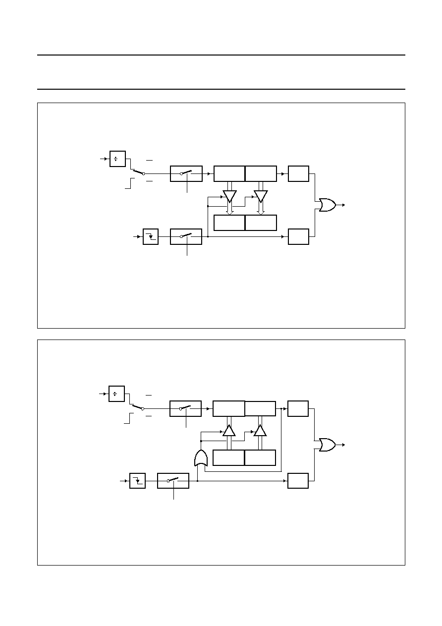
APTURE MODE
Figure 9 shows the Capture mode. Two options in this
mode may be selected by the EXEN2 bit in T2CON:
∑
If EXEN2 = 0, then Timer 2 is a 16-bit timer or counter
that sets the Timer 2 overflow bit (TF2) on overflow, this
can be used to generate an interrupt.
∑
If EXEN2 = 1, Timer 2 operates as already described
but with the additional feature that a HIGH-to-LOW
transition at external input T2EX causes the current
value in TL2 and TH2 to be captured into registers
RCAP2L and RCAP2H respectively. In addition, the
transition at T2EX causes the EXF2 bit in T2CON to be
set; this may also be used to generate an interrupt.
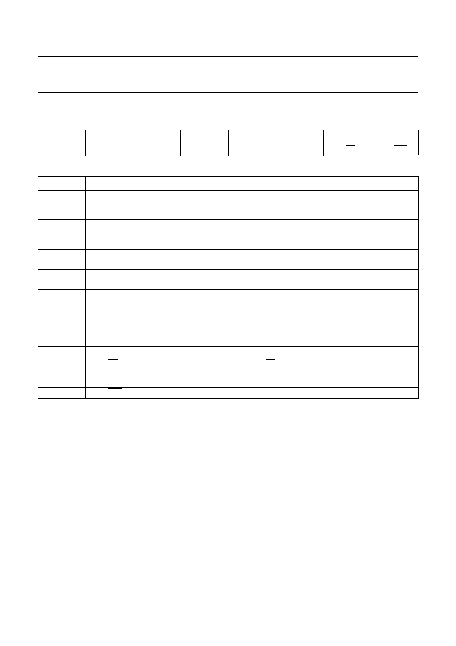
12.2.2
A
UTO
-
RELOAD MODE
Figure 10 shows the Auto-reload mode.
∑
Counting up (DCEN = 0)
In the Auto-reload mode and counting up, registers
RCAP2L/RCAP2H are used to hold a reload value for
TL2 /TH2 when Timer 2 rolls over. By setting/clearing bit
EXEN2 in T2CON the external trigger input pin T2EX
can be enabled/disabled. If EXEN2 = 0, then Timer 2 is
a 16-bit timer/counter which upon overflow sets TF2,
and reloads TL2/TH2 with the reload value held in
RCAP2L/RCP2H. If EXEN2 = 1, then Timer 2 performs
as above, but with the added feature that a
HIGH-to-LOW transition at pin T2EX causes the current
Timer 2 value (TL2/TH2 data) to be reloaded with the
value held in RCAP2L/RAP2H, and bit EXF2 in T2CON
to be set.
Timer 2 interrupt will be set if EXF2 is set or TF2 is set.
∑
Counting up (DCEN = 1 and T2EX = 1). In this mode
Timer 2 will count up. When the timer overflows (FFFFH
state), TF2 bit will be set. This will reload TL2 and TH2
with the contents of T2CAPL and T2CAPH, respectively.
Also bit EXF2 will be toggled. Bit EXF2 can be used as
the 17th bit if desired.
Timer 2 interrupt will be set only if TF2 is set.
∑
Counting down (DCEN = 1 and T2EX = 0. In this mode
Timer 2 will be counting down. Underflow will occur
when the contents of TL2/TH2 matches the contents of
RCAP2L/RCAP2H. A Timer 2 roll-over from
0000H to FFFFH is not considered as an underflow.
Upon underflow, bit TF2 will be set and registers
TL2/TH2 will be loaded with FFFFH. In addition, an
underflow will cause bit EXF2 to toggle, such that it can
be used as the 17th bit if desired.
Timer 2 interrupt will be set only if TF2 is set.
12.2.3
B
AUD
R
ATE
G
ENERATOR MODE
The Baud Rate Generator mode is selected when
RCLK0 = 1 or TCLK0 = 1 or RCLK1 = 1 or TCLK1 = 1.
It will be described in conjunction with the serial port
(UART); see Section 17.3.2.
1998 Aug 26
19
Philips Semiconductors
Product specification
Low voltage 8-bit microcontroller with
6-kbyte embedded RAM
SZF2002
Fig.9 Timer 2 in Capture mode.
handbook, full pagewidth
MGM136
TL2
(8 BITS)
TH2
(8 BITS)
RCAP2L
RCAP2H
EXF2
TF2
Timer 2
interrupt
EXEN2
control
transition
detector
T2EX PIN
capture
TR2
control
C/T2 = 0
C/T2 = 1
T2 PIN
6
fclk
Fig.10 Timer 2 in Auto-reload mode.
handbook, full pagewidth
MGM137
TL2
(8 BITS)
TR2
control
TH2
(8 BITS)
RCAP2L
RCAP2H
EXF2
TF2
Timer 2
interrupt
EXEN2
control
C/T2 = 0
C/T2 = 1
T2 PIN
6
fclk
transition
detector
T2EX PIN
reload
1998 Aug 26
20
Philips Semiconductors
Product specification
Low voltage 8-bit microcontroller with
6-kbyte embedded RAM
SZF2002
12.3
Timer/Counter 2 Control Register (T2CON)
Table 6
Timer/Counter 2 Control Register (SFR address C8H)
Table 7
Description of T2CON bits
7
6
5
4
3
2
1
0
TF2
EXF2
RCLK0
TCLK0
EXEN2
TR2
C/T2
CP/RL2
BIT
SYMBOL
DESCRIPTION
7
TF2
Timer 2 overflow flag. Set by a Timer 2 underflow or overflow and must be cleared by
software. TF2 will not be set when in either the Baud Rate generation mode or Clock out
mode.
6
EXF2
Timer 2 external flag. Set when either a capture or reload is caused by a negative
transition on T2EX and when EXEN2 = 1. In Auto-reload mode it is toggled on an
underflow or overflow. Cleared by software.
5
RCLK0
Receive clock 0 flag. When set, causes the UART to use Timer 2 overflow pulses.
RCLK0 = 0, causes Timer 1 overflow pulses to be used.
4
TCLK0
Transmit clock 0 flag. When set, causes the UART to use Timer 2 overflow pulses.
TCLK0 = 0, causes Timer 1 overflow pulses to be used.
3
EXEN2
Timer 2 external enable flag. When set, allows a capture or reload to occur, together
with an interrupt, as a result of a negative transition on input T2EX (if in Capture mode
or Auto-reload mode with DCEN reset). If in Auto-reload mode and DCEN is set, this bit
has no influence. In the other modes EXF2 is set and an interrupt is generated on a
HIGH-to-LOW transition on T2EX pin. In all modes EXEN2 = 0, causes Timer 2 to
ignore events at T2EX.
2
TR2
Timer 2 start/stop control. When TR2 = 1, Timer 2 is started.
1
C/T2
Timer or counter select for Timer 2. C/T2 = 0, selects the internal timer with a clock
frequency of
1
/
6
f
clk
. C/T2 = 1, selects the external event counter; negative edge
triggered.
0
CP/RL2
Capture/Reload flag. Selection of Capture or Auto-reload mode.
1998 Aug 26
21
Philips Semiconductors
Product specification
Low voltage 8-bit microcontroller with
6-kbyte embedded RAM
SZF2002
12.4
Timer/Counter 2 Mode Register (T2MOD)
Table 8
Timer/Counter 2 Mode Register (SFR address C9H)
Description of T2MOD bits
Table 9
Timer 2 operating modes; note 1
Note
1. X = don't care
7
6
5
4
3
2
1
0
-
-
RCLK1
TCLK1
-
T2RD
T2OE
DCEN
BIT
SYMBOL
DESCRIPTION
7
-
These 2 bits are reserved.
6
-
5
RCLK1
Receive Clock 1 flag. Reserved for future UART2. When set, causes the UART to use
Timer 2 overflow pulses. RCLK1 = 0, causes Timer 1 overflow pulses to be used.
4
TCLK1
Transmit Clock 1 flag. Reserved for future UART2. When set, causes the UART to use
Timer 2 overflow pulses. TCLK1 = 0, causes Timer 1 overflow pulses to be used.
3
-
This bit is reserved.
2
T2RD
Timer 2 Read flag. This bit is set by hardware if following a TL2 read and before a TH2
read, TH2 is incremented. It is reset on the trailing edge of the next TL2 read.
1
T2OE
Timer 2 Output Enable. When set, output is activated to output a clock at the T2 pin
(Clock output mode).
0
DCEN
Down Count Enable. When set, this allows Timer 2 to be configured as an up/down
counter.
RCLK0 + TCLK0 + RCLK1 + TCLK1
CP/RL2
T2OE
C/T2
MODE
0
0
0
X
16-bit Auto-reload
0
1
0
X
16-bit Capture
1
X
X
X
Baud Rate Generator
1998 Aug 26
22
Philips Semiconductors
Product specification
Low voltage 8-bit microcontroller with
6-kbyte embedded RAM
SZF2002
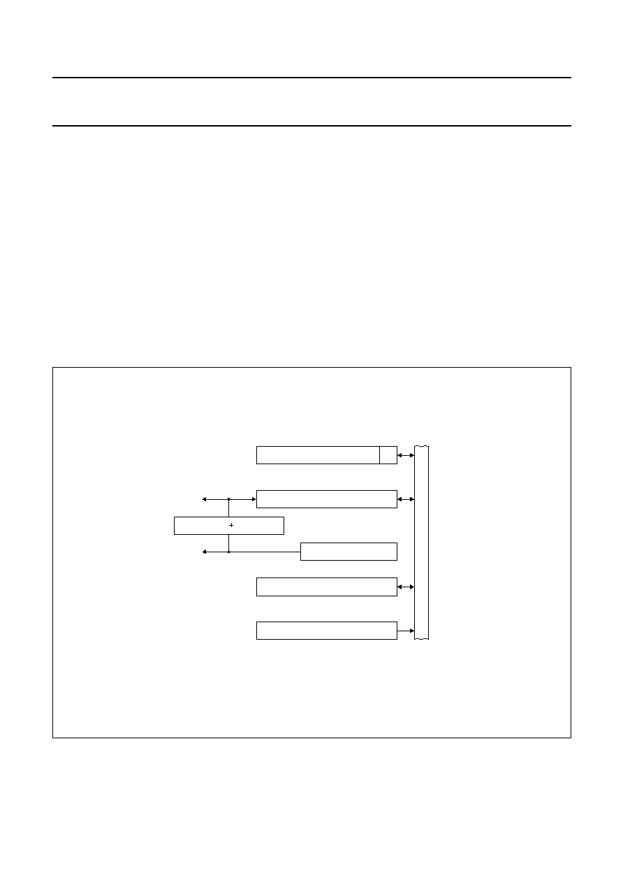
12.5
Watchdog Timer (T3)
In addition to Timer 2 and the standard timers, a Watchdog
Timer (consisting of an 11-bit prescaler and an 8-bit timer)
is also available.
The Watchdog Timer is controlled by the Watchdog
Enable Register (WDTKEY). When WDTKEY = 55H, the
timer is disabled and the Power-down mode is enabled.
Otherwise, the timer is enabled and the Power-down mode
is disabled. In the Idle mode the Watchdog Timer and reset
circuitry remain active.
The Watchdog Timer is shown in Fig.11.
The timer frequency is derived from the clock frequency
using the formula shown below:
When a timer overflow occurs, the microcontroller is reset.
To prevent a system reset the timer must be reloaded in
time by the application software.
f
timer
f
clk
6
2048
◊
(
)
T3
◊
-------------------------------------------
=
If the processor suffers a hardware/software malfunction,
the software will fail to reload the timer.This failure will
produce a reset upon overflow thus preventing the
processor running out of control.
The Watchdog Timer can only be reloaded if the condition
flag WLE (PCON.4) has been previously set by software.
At the moment the counter is loaded the condition flag is
automatically cleared. After reset the Watchdog Timer is
off. The Watchdog Timer is started by loading a value into
T3.
The time interval between the timer reloading and the
occurrence of a reset is dependent upon the reloaded
value. The time interval is derived from the clock and the
value programmed into T3 and may be calculated as
shown below:
For example, this time period may range from 2 to 500 ms
when using a clock frequency f
clk
= 6 MHz.
T
reload
256
T3
≠
(
)
f
timer
-----------------------------
=
Fig.11 Functional diagram of the Watchdog Timer (T3).
handbook, full pagewidth
MGM141
INTERNAL BUS
write
T3
PRESCALER
11-BIT
TIMER T3 (8-BIT)
LOAD
CLEAR
overflow
internal
reset
LOADEN
SFR WDTKEY
LOADEN
PCON.4
PCON.1
CLEAR
WLE
PD
R
RST
RST
INTERNAL BUS
fclk/6
1998 Aug 26
23
Philips Semiconductors
Product specification
Low voltage 8-bit microcontroller with
6-kbyte embedded RAM
SZF2002
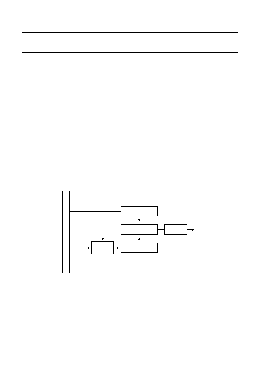
13 PULSE WIDTH MODULATED OUTPUT
One Pulse Width Modulated output channel PWM is
provided which outputs pulses of programmable length
and interval. The repetition frequency is defined by an 8-bit
prescaler (PWMP) that generates the clock for the
counter. The 8-bit counter counts modulo 255, i.e. from
0 to 254 inclusive. The value held in the 8-bit counter is
compared to the contents of the register PWM. If a new
prescaler value is written in register PWMP the 8-bit
counter finishes uninterrupted, and the new prescaler
value is used in the next count cycle.
Provided the contents of this register are greater than the
counter value, the PWM output is set HIGH. If the contents
of register PWMP are equal to, or less than the counter
value, the PWM output is set LOW.
The pulse-width-ratio is therefore defined by the contents
of register PWM. The pulse-width-ratio will be in the range
0 to
255
/
255
and may be programmed in increments of
1
/
255
.
The repetition frequency (f
PWM
) at the PWM output is given
by:
For f
clk
= 12 MHz, the above formula gives a repetition
frequency range of 92 Hz to 23.5 kHz.
By loading the PWM register with either 00H or FFH, the
PWM output can be retained at a constant LOW or HIGH
level respectively. When loading FFH into the PWM
register, the 8-bit counter will never actually reach this
value.
The PWM output pin is not shared with any other function.
f
PWM
f
clk
1
(
PWMP
)
255
◊
+
2
◊
-----------------------------------------------------------------
=
Fig.12 Functional diagram of Pulse Width Modulated output (PWM).
handbook, full pagewidth
MGM140
I
N
T
E
R
N
A
L
B
U
S
fclk
PWMP
+
DIVIDE-BY-2
8-BIT COUNTER
PWM
8-BIT COMPARATOR
OUTPUT
BUFFER
PWM
1998 Aug 26
24
Philips Semiconductors
Product specification
Low voltage 8-bit microcontroller with
6-kbyte embedded RAM
SZF2002
13.1
Prescaler Frequency Control Register (PWMP)
Table 10 Prescaler Frequency Control Register (SFR address FEH)
Table 11 Description of PWMP bits
13.2
Pulse Width Register (PWM)
Table 12 Pulse Width Register (SFR address FCH)
Table 13 Description of PWM bits
7
6
5
4
3
2
1
0
PWMP.7
PWMP.6
PWMP.5
PWMP.4
PWMP.3
PWMP.2
PWMP.1
PWMP.0
BIT
SYMBOL
DESCRIPTION
7 to 0
PWMP.7 to PWMP.0
prescaler division factor = (PWMP) + 1
7
6
5
4
3
2
1
0
PWM.7
PWM.6
PWM.5
PWM.4
PWM.3
PWM.2
PWM.1
PWM.0
BIT
SYMBOL
DESCRIPTION
7 to 0
PWM.7 to PWM.0
HIGH/LOW ratio of
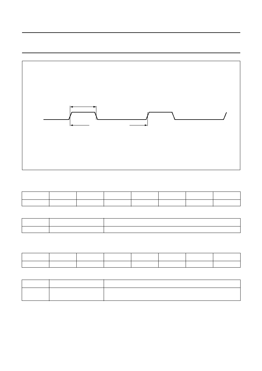
Fig.13 PWM signals.
handbook, full pagewidth
MGM186
PWM
PWM
◊
2
◊
(PWMP
+
1)
◊
tclk
255
◊
2
◊
(PWMP
+
1)
◊
tclk
PWM signal
PWM
(
)
255
PWM
(
)
≠
{
}
-----------------------------------------------
=
1998 Aug 26
25
Philips Semiconductors
Product specification
Low voltage 8-bit microcontroller with
6-kbyte embedded RAM
SZF2002
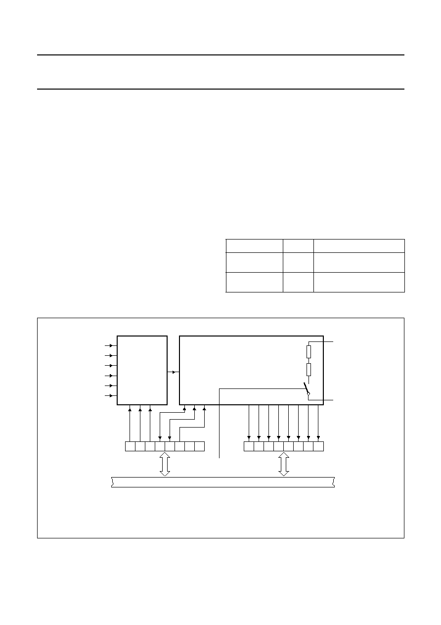
14 ANALOG-TO-DIGITAL CONVERTER (ADC)
The analog input circuitry consists of a 6-input analog
multiplexer and an ADC with 8-bit resolution. The analog
supply (V
DDA
) and analog ground (V
SSA
) are connected via
separate input pins. For clock frequencies higher than
8 MHz the clock prescaler is needed (divide-by-2).
The functional diagram of the ADC is shown in Fig.14.
The ADC is controlled using the ADC Control Register
(ADCON). Input channels are selected by the analog
multiplexer via the ADCON register bits AADR0 to AADR2.
A conversion is started by setting the ADCS bit in the
ADCON register. The completion of the 8-bit ADC
conversion is flagged by ADCI in the ADCON register,
which will generate an interrupt if this is enabled (EAD).
The result is stored in the Special Function Register ADCH
(address C5H).
To save power the ADC current is switched on only during
conversion and is independent of the processor mode
(active, Idle or Power-down). If the processor goes into Idle
or Power-down mode, the ADC interrupt must be used to
wake-up the CPU again.
While ADCS = 1 or ADCI = 1, a new ADC start will be
blocked and consequently lost, however an ADC
conversion already in progress will finish uninterrupted.
An ADC conversion already in progress is aborted when
the Power-down mode is entered. The result of a
completed conversion (ADCI = 1) remains unaffected
when entering the Idle or Power-down mode.
When no result of a completed conversion (ADCI = 0) is
available, the ADCON and ADCH registers will be reset
when entering the Power-down mode. Note that AADRx
and CKDIV have to be set explicitly to restore their
previous values for the first conversion after Power-down
mode.
Table 14 Conversion time in clock cycles
CONDITION
MAX.
REMARK
f
clk
8 MHz,
CKDIV = 0
288
normal conversion
f
clk
> 8 MHz,
CKDIV = 1
576
prescaler used
Fig.14 Functional diagram of analog input.
(1) For the descriptions of ADCON bits see Table 16.
handbook, full pagewidth
MGM187
ANALOG INPUT
MULTIPLEXER
8-BIT ADC
(succesive approximation)
ADCON
(1)
1
2
3
4
5
6
7
0
1
2
3
4
5
6
Power-down
7
0
V
DDA
V
SSA
ADCH
INTERNAL BUS
ADC0
ADC1
ADC2
ADC3
ADC4
ADC5
1998 Aug 26
26
Philips Semiconductors
Product specification
Low voltage 8-bit microcontroller with
6-kbyte embedded RAM
SZF2002
14.1
ADC Control Register (ADCON)
Table 15 ADC Control Register (SFR address C4H)
Table 16 Description of ADCON bits
Table 17 Selection of analog input channel
14.2
ADC Result Register (ADCH)
Table 18 ADC Result Register (SFR address C5H)
Table 19 Description of ADCH bits
7
6
5
4
3
2
1
0
-
-
CKDIV
ADCI
ADCS
AADR2
AADR1
AADR0
BIT
SYMBOL
DESCRIPTION
7
-
These 2 bits are reserved.
6
-
5
CKDIV
Prescaler select. When CKDIV = 1, the ADC clock prescaler is used (divide-by-2).
Prescaling is necessary with clocks over 8 MHz.
4
ADCI
ADC interrupt flag. This flag is set when an ADC conversion result is ready to be read.
An interrupt is invoked if this is enabled (EAD). This flag must be cleared by software,
(it cannot be set by software).
3
ADCS
ADC start and status flag. When this bit is set an ADC conversion is started. ADCS
must be set by software. The ADC logic ensures that this signal is HIGH while the ADC
is busy. On completion of the conversion ADCI is set and one clock later the ADCS flag
is reset. ADCS cannot be reset by software.
2
AADR2
Analog input select. These bits are used to select one of the six analog inputs;
see Table 17.
1
AADR1
0
AADR0
AADR2
AADR1
AADR0
SELECTED CHANNEL
0
0
0
ADC0
0
0
1
ADC1
0
1
0
ADC2
0
1
1
ADC3
1
0
0
ADC4
1
0
1
ADC5
1
1
0
reserved
1
1
1
reserved
7
6
5
4
3
2
1
0
ADC7
ADC6
ADC5
ADC4
ADC3
ADC2
ADC1
ADC0
BIT
SYMBOL
DESCRIPTION
7 to 0
ADC7 to ADC0
8-bit ADC result

1998 Aug 26
27
Philips Semiconductors
Product specification
Low voltage 8-bit microcontroller with
6-kbyte embedded RAM
SZF2002
15 REDUCED POWER MODES
There are two software selectable modes of reduced
activity for further power reduction: Idle and Power-down.
15.1
Idle mode
Idle mode operation permits the interrupt, serial ports,
timer blocks, PWM and ADC to continue to function while
the clock to the CPU is halted.
The following functions remain active during the Idle
mode:
∑
Timer 0, Timer 1, Timer 2 and Timer 3
(Watchdog Timer)
∑
UART, I
2
C-bus interface
∑
Internal interrupt
∑
External interrupt
∑
PWM
∑
ADC.
These functions may generate an interrupt or reset; thus
ending the Idle mode.
The instruction that sets bit IDL (PCON.0) is the last
instruction executed in the normal operating mode before
the Idle mode is activated. Once in Idle mode, the CPU
status is preserved along with the Stack Pointer, Program
Counter, Program Status Word, SFRs and Accumulator.
The RAM and all other registers maintain their data during
Idle mode. The status of the external pins during Idle mode
is shown in Table 20.
15.1.1
T
ERMINATION OF THE
I
DLE MODE USING AN
ENABLED INTERRUPT
Activation of any enabled interrupt will cause IDL
(PCON.0) to be cleared by hardware thus terminating the
Idle mode. The interrupt is serviced, and following the
RETI instruction, the next instruction to be executed will be
the one following the instruction that put the device in the
Idle mode. The flag bits GF0 (PCON.2) and GF1 (PCON.3)
may be used to determine whether the interrupt was
received during normal execution or during the Idle mode.
For example, the instruction that writes to PCON.0 can
also set or clear one or both flag bits. When the Idle mode
is terminated by an interrupt, the service routine can
examine the status of the flag bits.
15.1.2
T
ERMINATION OF THE
I
DLE MODE USING AN
EXTERNAL HARDWARE RESET
The second way of terminating the Idle mode is with an
external hardware reset, or an internal reset caused by an
overflow of Timer 3 (Watchdog Timer). Since the clock is
still running, the hardware reset is required to be active for
two machine cycles (12 clock periods) to complete the
reset operation. Reset redefines all SFRs but does not
affect the on-chip RAM.
15.2
Power-down mode
The Power-down operation freezes the SZF2002.
The Power-down mode can only be activated by setting
the PD bit in the PCON register.
The instruction that sets PD (PCON.1) is the last executed
prior to going into the Power-down mode. Once in the
Power-down mode, the internal clock is stopped.
The contents of the on-chip RAM and the SFRs are
preserved. The port pins output the value held by their
respective SFRs. OE is held HIGH, but CE is switched to
HIGH, so the external ROM will not be enabled during
power down, to save system power.
15.3
Wake-up from Power-down mode
Setting the PD flag in the PCON register forces the
controller into the Power-down mode. Setting this flag
enables the controller to be woken-up from the
Power-down mode with either the external interrupts
INT0 to INT8, or a reset operation. The wake-up operation
has two basic approaches as explained in
Section 15.3.1 and 15.3.2.
15.3.1
W
AKE
-
UP USING
INT0
TO
INT8
If any of the interrupts INT0 to INT8 is enabled, the device
can be woken-up from the Power-down mode with these
external interrupts. The user must ensure that the external
clock is stable before the controller restarts, the internal
clock will remain inactive for 18 clock periods. This is
controlled by an on-chip delay counter.
15.3.2
W
AKE
-
UP USING
RST
To wake-up the SZF2002, the RST pin must be kept HIGH
for a minimum of 12 clock cycles. The user must ensure
that the external clock is stable before the controller
restarts (at RST falling edge), the internal clock will remain
inactive for 18 clock periods. This is controlled by an
on-chip delay counter.
1998 Aug 26
28
Philips Semiconductors
Product specification
Low voltage 8-bit microcontroller with
6-kbyte embedded RAM
SZF2002
15.4
Status of external pins
The status of the external pins during Idle and Power-down mode is shown in Table 20.
Table 20 Status of external pins during Idle and Power-down modes
15.5
Power Control Register (PCON)
Idle and Power-down modes are activated by software using this SFR. PCON is not bit addressed, the reset value of
PCON is 00000000B.
Table 21 Power Control Register (SFR address 87H)
Table 22 Description of PCON bits
MODE
MEMORY
CE
OE
PWM
PORTS 1, 3
AND 4
DATA BUS
Idle
internal
1
1
active
port data
Port 0 data
external
1
1
active
port data
floating
Power-down
internal
1
1
halted in last state
port data
Port 0 data
external
1
1
halted in last state
port data
floating
7
6
5
4
3
2
1
0
SMOD
ARD
RFI
WLE
GF1
GF0
PD
IDL
BIT
SYMBOL
DESCRIPTION
7
SMOD
Double Baud rate. When set to a logic 1 the baud rate is doubled when the serial port
SIO0 is being used in modes 1, 2 or 3 (except when Timer 2 is used).
6
ARD
Setting this bit will force all MOVX instructions to access off-chip memory instead of
AUX RAM.
5
RFI
RFI reduction mode. Setting this bit will disable the ALE toggling during on-chip
memory access. The SZF2002 does not have this signal during operational mode, but
setting this bit will reduce the number of chip selects (CE) of the external memory (and
thus power).
4
WLE
Watchdog Load Enable. This flag must be set by software prior to loading the
Watchdog Timer (T3). It is cleared when T3 is loaded.
3
GF1
General purpose flag 1.
2
GF0
General purpose flag 0.
1
PD
Power-down mode selection. Setting this bit activates the Power-down mode. If a
logic 1 is written to both PD and IDL at the same time, PD takes precedence.
0
IDL
Idle mode selection. Setting this bit activates the Idle mode.
1998 Aug 26
29
Philips Semiconductors
Product specification
Low voltage 8-bit microcontroller with
6-kbyte embedded RAM
SZF2002
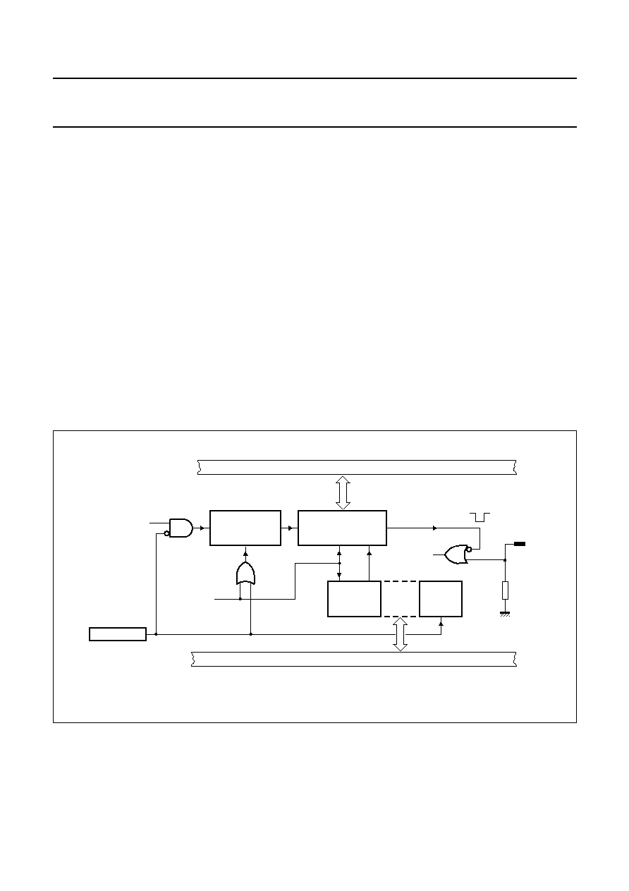
16 I
2
C-BUS SERIAL I/O
The serial port supports the twin line I
2
C-bus, which
consists of a data line (SDA) and a clock line (SCL). These
lines also function as the I/O port lines P1.7 and P1.6
respectively.
The system is unique because data transport, clock
generation, address recognition and bus control arbitration
are all controlled by hardware.
The I
2
C-bus serial I/O has complete autonomy in byte
handling and operates in 4 modes:
∑
Master transmitter
∑
Master receiver
∑
Slave transmitter
∑
Slave receiver.
These functions are controlled by the Serial Control
Register (S1CON). S1STA is the Status Register whose
contents may also be used as a vector to various service
routines. S1DAT is the Data Shift Register and S1ADR is
the Slave Address Register. Slave address recognition is
performed by on-chip hardware.
Figure 15 shows the block diagram of the I
2
C-bus
serial I/O.
Fig.15 Block diagram of I
2
C-bus serial I/O.
MLB199
SLAVE ADDRESS
S1ADR
GC
SHIFT REGISTER
S1DAT
SDA
ARBITRATION SYNC LOGIC
SCL
BUS CLOCK GENERATOR
S1STA
INTERNAL BUS
7
0
S1CON
7
0
7
0
7
0
CONTROL REGISTER
STATUS REGISTER

1998 Aug 26
30
Philips Semiconductors
Product specification
Low voltage 8-bit microcontroller with
6-kbyte embedded RAM
SZF2002
16.1
Serial Control Register (S1CON)
Table 23 Serial Control Register (SFR address D8H)
Table 24 Description of S1CON bits
7
6
5
4
3
2
1
0
CR2
ENS1
STA
STO
SI
AA
CR1
CR0
BIT
SYMBOL
DESCRIPTION
6
ENS1
Enable serial I/O. When ENS1 = 0, the serial I/O is disabled. SDA and SCL outputs are
in the high-impedance state; P1.6 and P1.7 function as open-drain ports. When
ENS1 = 1, the serial I/O is enabled. Output port latches P1.6 and P1.7 must be set to
logic 1.
5
STA
START flag. When this bit is set in Slave mode, the SIO hardware checks the status of
the I
2
C-bus and generates a START condition if the bus is free or after the bus becomes
free. If STA is set while the SIO is in Master mode, SIO will generate a repeated START
condition.
4
STO
STOP flag. With this bit set while in Master mode a STOP condition is generated. When
a STOP condition is detected on the I
2
C-bus, the SIO hardware clears the STO flag.
STO may also be set in Slave mode in order to recover from an error condition. In this
case no STOP condition is transmitted to the I
2
C-bus. However, the SIO hardware
behaves as if a STOP condition has been received and releases the SDA and SCL
lines. The SIO then switches to the not addressed Slave receiver mode. The STOP flag
is cleared by the hardware.
3
SI
SIO interrupt flag. This flag is set and an interrupt is generated, after any of the
following events occur:
∑
A START condition is generated in Master mode
∑
Own slave address has been received during AA = 1
∑
The general call address has been received while GC (S1ADR.0) = 1 and AA = 1
∑
A data byte has been received or transmitted in Master mode (even if arbitration is lost)
∑
A data byte has been received or transmitted as selected slave
∑
A STOP or START condition is received as selected slave receiver or transmitter.
2
AA
Assert Acknowledge. When this bit is set, an acknowledge (LOW level to SDA) is
returned during the acknowledge clock pulse on the SCL line when:
∑
Own slave address is received
∑
General call address is received; GC (S1ADR.0) = 1
∑
A data byte is received while the device is programmed to be a Master receiver
∑
A data byte is received while the device is a selected Slave receiver.
When this bit is reset, no acknowledge is returned. Consequently, no interrupt is
requested when the own slave address or general call address is received.
7
CR2
Clock Rate selection. These 3 bits determine the serial clock frequency when SIO is in
the Master mode. See Table 25.
1
CR1
0
CR0
1998 Aug 26
31
Philips Semiconductors
Product specification
Low voltage 8-bit microcontroller with
6-kbyte embedded RAM
SZF2002
Table 25 Selection of the serial clock frequency (SCL) in a Master mode of operation
16.2
Serial Status Register (S1STA)
S1STA is a read-only register. The contents of this register may be used as a vector to a service routine. This optimizes
the response time of the software and consequently that of the I
2
C-bus. The status codes for all possible modes of the
I
2
C-bus interface is given in Table 29. The register has only a valid vector to a service routine if the SI bit of the S1CON
register is set, otherwise it is invalid, usually F8H.
Table 26 Serial Status Register (SFR address D9H)
Table 27 Description of S1STA bits
Table 28 Symbols used in Table 29
CR2
CR1
CR0
f
clk
DIVISOR
BIT RATE (kHz) AT f
clk
= 1 MHz
0
0
0
128
7.81
0
0
1
112
8.93
0
1
0
96
10.42
0
1
1
80
12.50
1
0
0
480
2.08
1
0
1
60
16.67
1
1
0
30
33.33
1
1
1
reserved
-
7
6
5
4
3
2
1
0
SC4
SC3
SC2
SC1
SC0
0
0
0
BIT
SYMBOL
DESCRIPTION
3 to 7
SC4 to SC0
5-bit status code; see Table 29.
0 to 2
-
These three bits are always zero.
SYMBOL
DESCRIPTION
SLA
7-bit slave address
R
read bit
W
write bit
ACK
acknowledgement (acknowledge bit is logic 0)
ACK
no acknowledgement (acknowledge bit is logic 1)
DATA
data byte to or from I
2
C-bus
MST
master
SLV
slave
TRX
transmitter
REC
receiver
1998 Aug 26
32
Philips Semiconductors
Product specification
Low voltage 8-bit microcontroller with
6-kbyte embedded RAM
SZF2002
Table 29 Status codes
S1STA VALUE
DESCRIPTION
MST/TRX mode
08H
A START condition has been transmitted.
10H
A repeated START condition has been transmitted.
18H
SLA and W have been transmitted, ACK has been received.
20H
SLA and W have been transmitted, ACK received.
28H
DATA of S1DAT has been transmitted, ACK received.
30H
DATA of S1DAT has been transmitted, ACK received.
38H
Arbitration lost in SLA, R/W or DATA.
MST/REC mode
08H
A START condition has been transmitted.
10H
A repeated START condition has been transmitted.
38H
Arbitration lost while returning ACK.
40H
SLA and R have been transmitted, ACK received.
48H
SLA and R have been transmitted, ACK received.
50H
DATA has been received, ACK returned.
58H
DATA has been received, ACK returned.
SLV/REC mode
60H
Own SLA and W have been received, ACK returned.
68H
Arbitration lost in SLA, R/W as MST. Own SLA and W have been received, ACK returned.
70H
General CALL has been received, ACK returned.
78H
Arbitration lost in SLA, R/W as MST. General CALL has been received.
80H
Previously addressed with own SLA. DATA byte received, ACK returned.
88H
Previously addressed with own SLA. DATA byte received, ACK returned.
90H
Previously addressed with general CALL. DATA byte has been received, ACK has been returned.
98H
Previously addressed with general CALL. DATA byte has been received, ACK has been returned.
A0H
A STOP condition or repeated START condition has been received while still addressed as SLV/REC
or SLV/TRX.
SLV/TRX mode
A8H
Own SLA and R have been received, ACK returned.
B0H
Arbitration lost in SLA and R/W as MST. Own SLA and R have been received, ACK returned.
B8H
DATA byte has been transmitted, ACK received.
C0H
DATA byte has been transmitted, ACK received.
C8H
Last DATA byte has been transmitted (AA = 0), ACK received.
Miscellaneous
00H
Bus error during MST mode or selected SLV mode, due to an erroneous START or STOP condition.
F8H
No relevant state information available, SI = 0.
1998 Aug 26
33
Philips Semiconductors
Product specification
Low voltage 8-bit microcontroller with
6-kbyte embedded RAM
SZF2002
16.3
Data Shift Register (S1DAT)
S1DAT contains the serial data to be transmitted or data which has just been received. The MSB (bit 7) is transmitted or
received first; i.e. data shifted from right to left. The data received is only valid while the SI bit of the S1CON register is set.
Table 30 Data Shift Register (SFR address DAH)
16.4
Address Register (S1ADR)
This 8-bit register may be loaded with the 7-bit slave address to which the controller will respond when programmed as
a slave receiver/transmitter.
Table 31 Address Register (SFR address DBH)
Table 32 Description of S1ADR bits
7
6
5
4
3
2
1
0
S1DAT.7
S1DAT.6
S1DAT.5
S1DAT.4
S1DAT.3
S1DAT.2
S1DAT.1
S1DAT.0
7
6
5
4
3
2
1
0
SLA6
SLA5
SLA4
SLA3
SLA2
SLA1
SLA0
GC
BIT
SYMBOL
DESCRIPTION
7 to 1
SLA6 to
SLA0
Own slave address.
0
GC
This bit is used to determine whether the general call address is recognized. When
GC = 0, the general call address is not recognized; when GC = 1, the general call
address is recognized.

1998 Aug 26
34
Philips Semiconductors
Product specification
Low voltage 8-bit microcontroller with
6-kbyte embedded RAM
SZF2002
17 STANDARD SERIAL INTERFACE SIO0: UART
This serial port is full duplex which means that it can
transmit and receive simultaneously. It is also
receive-buffered and can commence reception of a
second byte before a previously received byte has been
read from the register. (However, if the first byte has not
been read by the time the reception of the second byte is
complete, one of the bytes will be lost). The serial port
receive and transmit registers are both accessed via the
Special Function Register S0BUF. Writing to S0BUF loads
the transmit register and reading S0BUF accesses a
physically separate receive register.
The serial port can operate in 4 modes:
Mode 0 Serial data enters and exits through RXD. TXD
outputs the shift clock. 8 bits are
transmitted/received (LSB first). The baud rate is
fixed at
1
/
6
f
clk
. See Figs 17 and 18.
Mode 1 10 bits are transmitted (through TXD) or received
(through RXD): a start bit (logic 0), 8 data bits
(LSB first), and a stop bit (logic 1). On receive,
the stop bit goes into RB8 in the SFR S0CON.
The baud rate is variable. See Figs 19 and 20.
Mode 2 11 bits are transmitted (through TXD) or received
(through RXD): start bit (logic 0), 8 data bits (LSB
first), a programmable 9th data bit, and a stop bit
(logic 1). On transmit, the 9th data bit (TB8 in
S0CON) can be assigned the value of a logic 0 or
logic 1. Or, for example, the parity bit (P, in the
PSW) could be moved into TB8. On receive, the
9th data bit goes into RB8 in S0CON, while the
stop bit is ignored. The baud rate is
programmable to either
1
/
16
or
1
/
32
f
clk
.
See Figs 21 and 22.
Mode 3 11 bits are transmitted (through TXD) or received
(through RXD): a start bit (logic 0), 8 data bits
(LSB first), a programmable 9th data bit and a
stop bit (logic 1). In fact, Mode 3 is the same as
Mode 2 in all respects except baud rate.
The baud rate in Mode 3 is variable.
See Figs 23 and 24.
In all four modes, transmission is initiated by any
instruction that uses S0BUF as a destination register.
Reception is initiated in Mode 0 by the condition RI = 0 and
REN = 1. Reception is initiated in the other modes by the
incoming start bit if REN = 1.
17.1
Multiprocessor communications
Modes 2 and 3 have a special provision for multiprocessor
communications. In these modes, 9 data bits are received.
The 9th bit goes into RB8. The following bit is the stop bit.
The port can be programmed such that when the stop bit
is received, the serial port interrupt will be activated, but
only if RB8 = 1. This feature is enabled by setting bit SM2
in S0CON. One use of this feature, in multiprocessor
systems, is as follows.
When the master processor wants to transmit a block of
data to one of several slaves, it first sends out an address
byte which identifies the target slave. An address byte
differs from a data byte in that the 9th bit is HIGH in an
address byte and LOW in a data byte. With SM2 = 1, no
slave will be interrupted by a data byte. An address byte,
however, will interrupt all slaves, so that each slave can
examine the received byte and see if it is being addressed.
The addressed slave will clear its SM2 bit and prepare to
receive the data bytes that will be sent. The slaves that
were not being addressed leave their SM2 bits set and go
on about their business, ignoring the coming data bytes.
SM2 has no effect in Mode 0, and in Mode 1 can be used
to check the validity of the stop bit. In a Mode 1 reception,
if SM2 = 1, the receive interrupt will not be activated unless
a valid stop bit is received.
1998 Aug 26
35
Philips Semiconductors
Product specification
Low voltage 8-bit microcontroller with
6-kbyte embedded RAM
SZF2002
17.2
Serial Port Control and Status Register (S0CON)
The Serial Port Control and Status Register is the Special Function Register S0CON. The register contains not only the
mode selection bits, but also the 9th data bit for transmit and receive (TB8 and RB8), and the serial port interrupt bits
(TI and RI).
Table 33 Serial Port Control Register (SFR address 98H)
Table 34 Description of S0CON bits
Table 35 Selection of the serial port modes
7
6
5
4
3
2
1
0
SMO
SM1
SM2
REN
TB8
RB8
TI
RI
BIT
SYMBOL
DESCRIPTION
7
SM0
Mode select. These 2 bits are used to select the serial port mode; see Table 35.
6
SM1
5
SM2
Enables the multiprocessor communication feature in Modes 2 and 3. In these modes, if
SM2 = 1, then RI will not be activated if the received 9th data bit (RB8) is a logic 0.
In Mode 1, if SM2 = 1, then RI will not be activated unless a valid stop bit was received.
In Mode 0, SM2 should be a logic 0.
4
REN
Enable serial reception. REN is set by software to enable reception, and cleared by
software to disable reception.
3
TB8
Is the 9th data bit that will be transmitted in Modes 2 and 3. Set or cleared by software
as desired.
2
RB8
In Modes 2 and 3, is the 9th data bit received. In Mode 1, if SM2 = 0, then RB8 is the
stop bit that was received. In Mode 0, RB8 is not used.
1
TI
Transmit interrupt flag. Set by hardware at the end of the 8th bit time in Mode 0, or at
the beginning of the stop bit time in the other modes, in any serial transmission. Must be
cleared by software.
0
RI
Receive interrupt flag. Set by hardware at the end of the 8th bit time in Mode 0, or
halfway through the stop bit time in the other modes, in any serial transmission (except
see SM2). Must be cleared by software.
SMO
SM1
MODE
DESCRIPTION
BAUD RATE
0
0
Mode 0
shift register
1
/
6
f
clk
0
1
Mode 1
8-bit UART
variable
1
0
Mode 2
9-bit UART
1
/
16
f
clk
or
1
/
32
f
clk
1
1
Mode 3
9-bit UART
variable

1998 Aug 26
36
Philips Semiconductors
Product specification
Low voltage 8-bit microcontroller with
6-kbyte embedded RAM
SZF2002
17.3
Baud rates
The baud rate in Mode 0 is fixed and may be calculated as:
The baud rate in Mode 2 depends on the value of the
SMOD bit in Special Function Register PCON and may be
calculated as:
∑
If SMOD = 0 (value on reset), the baud rate is
1
/
32
f
clk
∑
If SMOD = 1, the baud rate is
1
/
16
f
clk
.
17.3.1
U
SING
T
IMER
1
TO GENERATE BAUD RATES
When Timer 1 is used as the Baud Rate Generator, the
baud rates in Modes 1 and 3 are determined by the
Timer 1 overflow rate and the value of the SMOD bit as
follows:
The Timer 1 interrupt should be disabled in this
application. The timer itself can be configured for either
`timer' or `counter' operation in any of its 3 running modes.
In typical applications, it is configured for `timer' operation,
in the Auto-reload mode (high nibble of TMOD = 0010B).
In this case the baud rate is given by:
By configuring Timer 1 to run as a 16-bit timer (high nibble
of TMOD = 0001B), and using the Timer 1 interrupt to do
a 16-bit software reload, very low baud rates can be
achieved.
17.3.2
U
SING
T
IMER
2
TO GENERATE BAUD RATES
Timer 2 is selected as a Baud Rate Generator by setting
the RCLK0, TCLK0, RCLK1, or TCLK1 bit in T2CON.
The Baud Rate Generator mode is similar to the
Auto-reload mode, in that a roll-over in TH2 causes
Timer 2 registers to be reloaded with the 16-bit value held
in the registers RCAP2H and RCAP2L, which are preset
by software.
Baud rate
f
clk
6
-------
=
Baud rate
2
SMOD
32
-----------------
f
clk
◊
=
Baud rate
2
SMOD
32
-----------------
Timer 1 overflow rate
◊
=
Baud rate
2
SMOD
32
-----------------
f
clk
6
256
TH1
≠
(
)
◊
{
}
-----------------------------------------------------
◊
=
Baud rates in Modes 1 and 3 are determined by Timer 2's
overflow rate as specified below:
Timer 2 can be configured for either `timer' or `counter'
operation. In the most typical applications, it is configured
for `timer' operation (C/T2 = 0). `Timer' operation is slightly
different for Timer 2 when it is being used as a Baud Rate
Generator. Normally, as a timer it would increment every
machine cycle at a frequency of
1
/
6
f
clk
. However, as a Baud
Rate Generator it increments every state time at a
frequency of f
clk
. In this case, the baud rate in Modes 1 and
3 is determined as shown by the following equation:
Where (RCAP2H; RCAP2L) is the content of registers
RCAP2H and RCAP2L taken as a 16-bit unsigned integer.
Note that the maximum baud rate depends on clock
frequency and is determined by the following equation:
The Baud Rate Generator mode for Timer 2 is shown in
Fig.16. This figure is only valid if RCLK0 = 1 or TCLK0 = 1
or RCLK1 = 1 or TCLK1 = 1. At roll-over TH2 does not set
the TF2 bit in T2CON and therefore, will not generate an
interrupt. Consequently, the Timer 2 interrupt does not
need to be disabled when in the Baud Rate Generator
mode. If EXEN2 is set, a HIGH-to-LOW transition on T2EX
will set the EXF2 bit, also in T2CON, but will not cause a
reload from (RCAP2H; RCAP2L) to (TH2 and TL2).
Therefore, in this mode T2EX may be used as an
additional external interrupt.
When Timer 2 is operating as a timer (TR2 = 1), in the
Baud Rate Generator mode, registers TH2 and TL2 should
not be accessed (read or write). Under these conditions
the timer increments every state time and therefore the
results of a read or write may not be accurate.
The registers RCAP2H and RCAP2L however, may be
read but not written to. A write might overlap a reload and
cause write and/or reload errors. If a write operation is
required, Timer 2 or RCAP2H/RCAP2L should first be
turned off by clearing the TR2 bit.
Baud rate
Timer 2 overflow rate
16
--------------------------------------------------------
=
Baud rate
f
clk
16
65536
RCAP2H; RCAP2L
(
)
≠
{
}
◊
------------------------------------------------------------------------------------------------------
=
Maximum baud rate
f
clk
16
6
◊
----------------
=
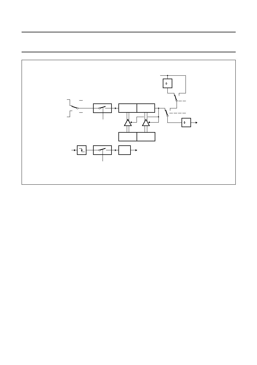
1998 Aug 26
37
Philips Semiconductors
Product specification
Low voltage 8-bit microcontroller with
6-kbyte embedded RAM
SZF2002
Fig.16 Timer 2 in Baud Rate Generator mode.
handbook, full pagewidth
MGM138
TL2
(8 BITS)
TH2
(8 BITS)
RCAP2L
RCAP2H
EXF2
TIMER 2 interrupt
(additional external interrupt)
16
RTCLK
RELOAD
CLK
UART receive/
transmit clock
SMOD
1
0
1
0
2
TIMER 1
overflow
EXEN2
control
transition
detector
T2EX PIN
TR2
control
C/T2 = 0
C/T2 = 1
T2 PIN
fclk
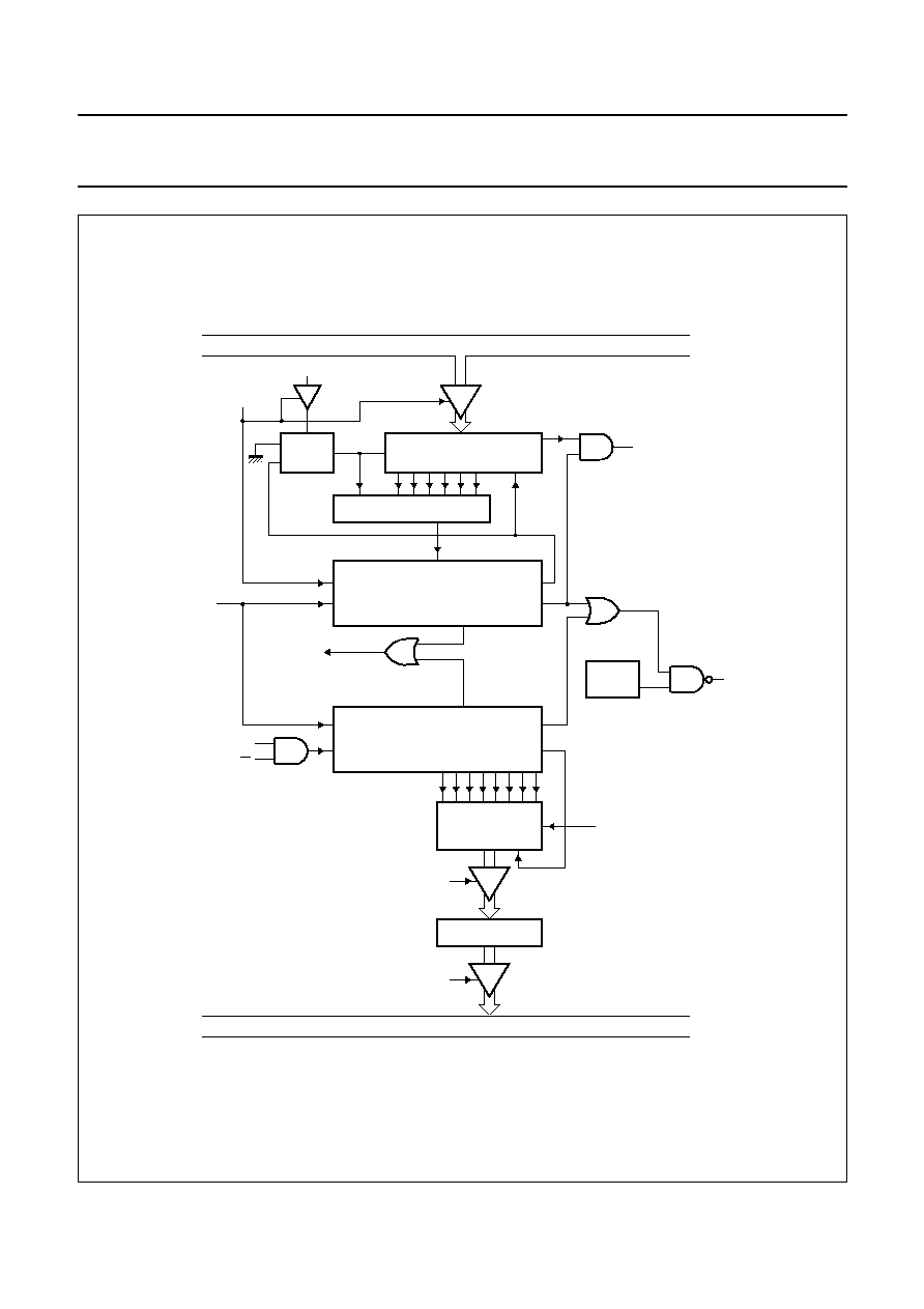
1998 Aug 26
38
Philips Semiconductors
Product specification
Low voltage 8-bit microcontroller with
6-kbyte embedded RAM
SZF2002
Fig.17 Serial port Mode 0.
handbook, full pagewidth
MGC752
START
SHIFT
T1
TX CONTROL
TX CLOCK
SEND
serial port
interrupt
RX CLOCK
R1
SHIFT
RX CONTROL
START
INPUT SHIFT
REGISTER
S0 BUFFER
INTERNAL BUS
READ
SBUF
SHIFT
LOAD
SBUF
S0 BUFFER
ZERO DETECTOR
SHIFT
D
CL
S
Q
INTERNAL BUS
TB8
write to
SBUF
1 1 1 1 1 1 1 0
REN
S6
RI
RXD
P3.0 ALT
output
function
RECEIVE
SHIFT
CLOCK
TXD
P3.1 ALT
output
function
RXD
P3.0 ALT
input
function
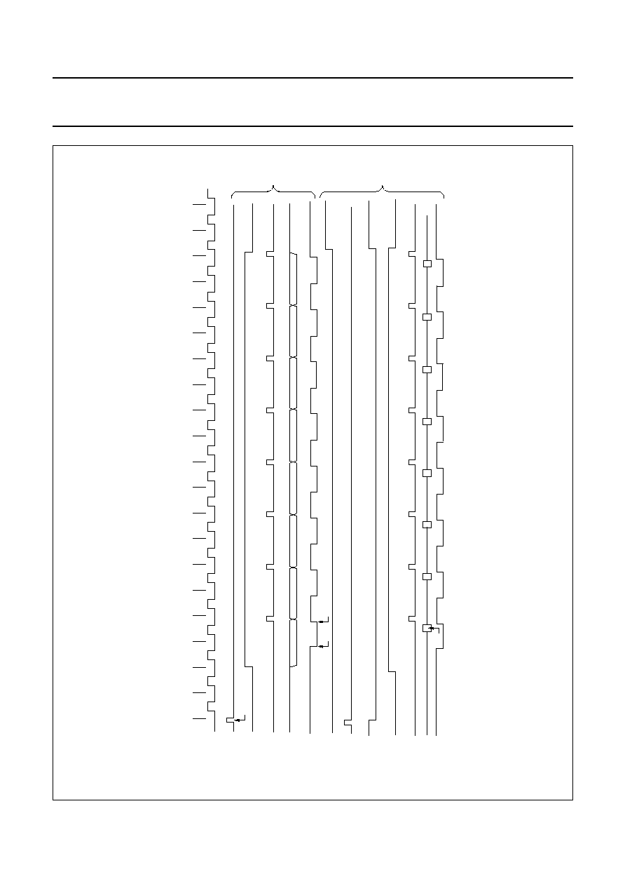
1998
Aug
26
39
Philips Semiconductors
Product specification
Low voltage 8-bit microcontroller with
6-kbyte embedded RAM
SZF2002
This text is here in white to force landscape pages to be rotated correctly when browsing through the pdf in the Acrobat reader.This text is here in
_
white to force landscape pages to be rotated correctly when browsing through the pdf in the Acrobat reader.This text is here inThis text is here in
white to force landscape pages to be rotated correctly when browsing through the pdf in the Acrobat reader. white to force landscape pages to be ...
handbook, full pagewidth
MLA567
s1...s6
s1...s6 s1...s6 s1...s6 s1...s6 s1...s6 s1...s6
s1...s6 s1...s6
s1...s6 s1...s6 s1...s6
s1...s6 s1...s6
s1...s6
s1...s6 s1...s6 s1...s6 s1...s6
s1...s6
...s6
WRITE TO SBUF
S6P2
D0
D1
D2
D3
D4
D5
D6
D7
S3P1
S6P1
WRITE TO SCON (CLEAR R1)
D0
D1
D2
D3
D4
D5
D6
D7
S5P2
ALE
SEND
SHIFT
RXD (DATA OUT)
TSC (SHIFT CLOCK)
RI
T1
RECEIVE
SHIFT
RXD (DATA IN)
TXD (SHIFT CLOCK)
T
R
A
N
S
M
I
T
R
E
C
E
I
V
E
Fig.18 Serial port Mode 0 timing.
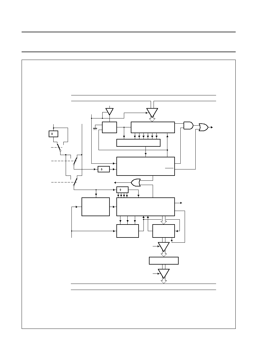
1998 Aug 26
40
Philips Semiconductors
Product specification
Low voltage 8-bit microcontroller with
6-kbyte embedded RAM
SZF2002
Fig.19 Serial port Mode 1.
handbook, full pagewidth
MGM145
START
SHIFT
DATA
T1
TX CONTROL
TX CLOCK
SEND
16
serial port
interrupt
16
RX CLOCK
R1
LOAD
SBUF
SHIFT
RX CONTROL
START
sample
INPUT SHIFT
REGISTER
(9-BITS)
BIT
DETECTOR
S0 BUFFER
INTERNAL BUS
READ
SBUF
SHIFT
LOAD
SBUF
S0 BUFFER
ZERO DETECTOR
SHIFT
D
CL
S
Q
TB8
INTERNAL BUS
write to
SBUF
RXD
TXD
HIGH-TO-LOW
TRANSITION
DETECTOR
0
SMOD
TCLK0
1
0
1
0
1
2
Timer 1
overflow
Timer 2
overflow
RCLK0
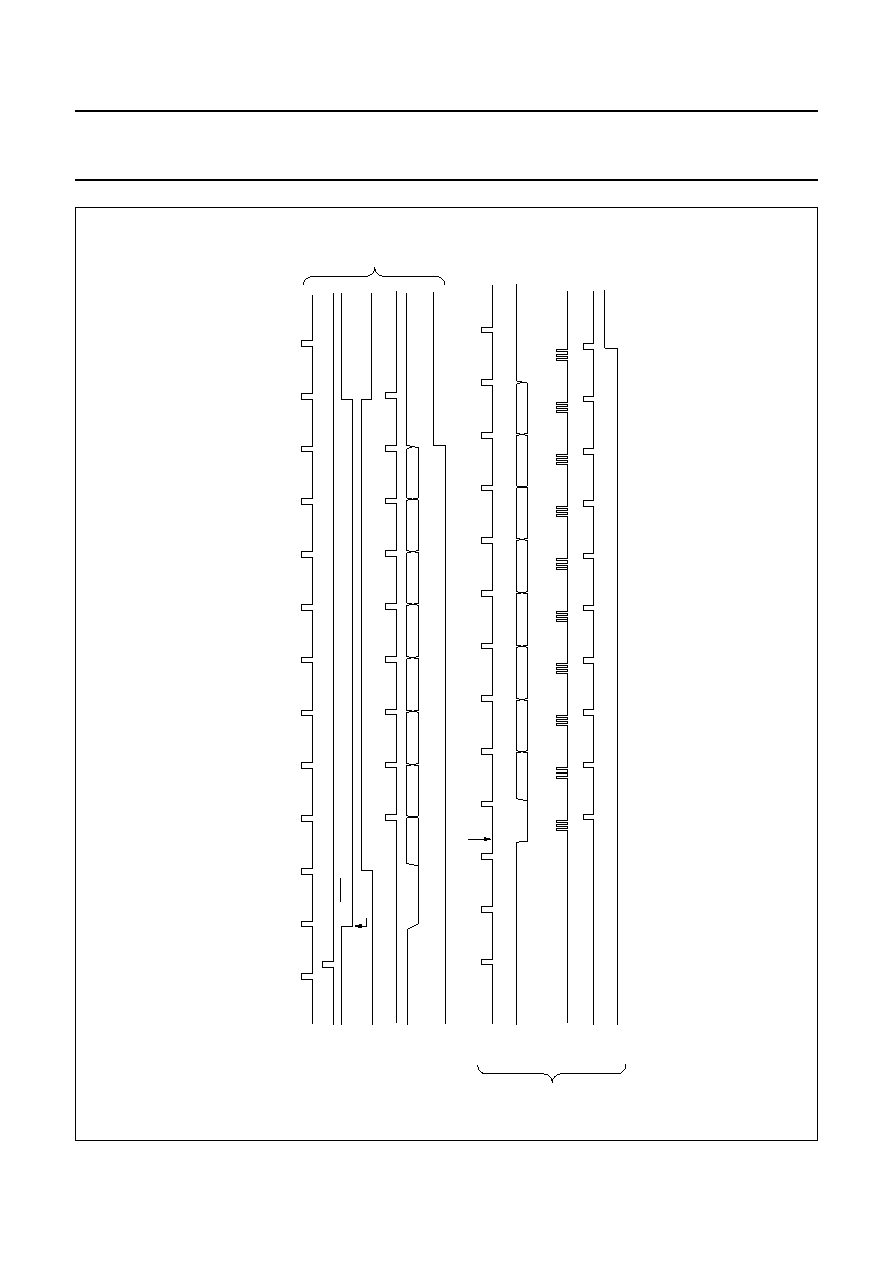
1998
Aug
26
41
Philips Semiconductors
Product specification
Low voltage 8-bit microcontroller with
6-kbyte embedded RAM
SZF2002
This text is here in white to force landscape pages to be rotated correctly when browsing through the pdf in the Acrobat reader.This text is here in
_
white to force landscape pages to be rotated correctly when browsing through the pdf in the Acrobat reader.This text is here inThis text is here in
white to force landscape pages to be rotated correctly when browsing through the pdf in the Acrobat reader. white to force landscape pages to be ...
handbook, full pagewidth
MLA569
D0
D1
D2
D3
D4
D5
D6
D7
START BIT
D0
D1
D2
D3
D4
D5
D6
D7
TX CLOCK
WRITE TO SBUF
DATA
SHIFT
TXD
TI
START BIT
S1P1
STOP BIT
˜
16 RESET
RX CLOCK
RXD
STOP BIT
BIT DETECTOR SAMPLE TIME
SHIFT
RI
SEND
T
R
A
N
S
M
I
T
R
E
C
E
I
V
E
Fig.20 Serial port Mode 1 timing.
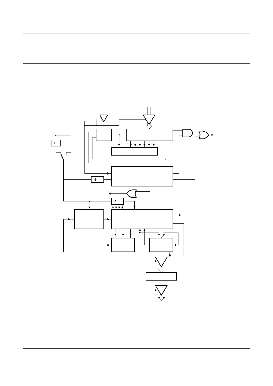
1998 Aug 26
42
Philips Semiconductors
Product specification
Low voltage 8-bit microcontroller with
6-kbyte embedded RAM
SZF2002
Fig.21 Serial port Mode 2.
handbook, full pagewidth
MGM144
START
STOP BIT
SHIFT
DATA
T1
TX CONTROL
TX CLOCK
SEND
16
serial port
interrupt
16
RX CLOCK
R1
LOAD
SBUF
SHIFT
RX CONTROL
START
sample
INPUT SHIFT
REGISTER
(9-BITS)
BIT
DETECTOR
S0 BUFFER
INTERNAL BUS
READ
SBUF
SHIFT
LOAD
SBUF
S0 BUFFER
ZERO DETECTOR
SHIFT
D
CL
S
Q
TB8
INTERNAL BUS
write to
SBUF
2
fclk
RXD
TXD
0
SMOD at
PCON.7
1
HIGH-TO-LOW
TRANSITION
DETECTOR
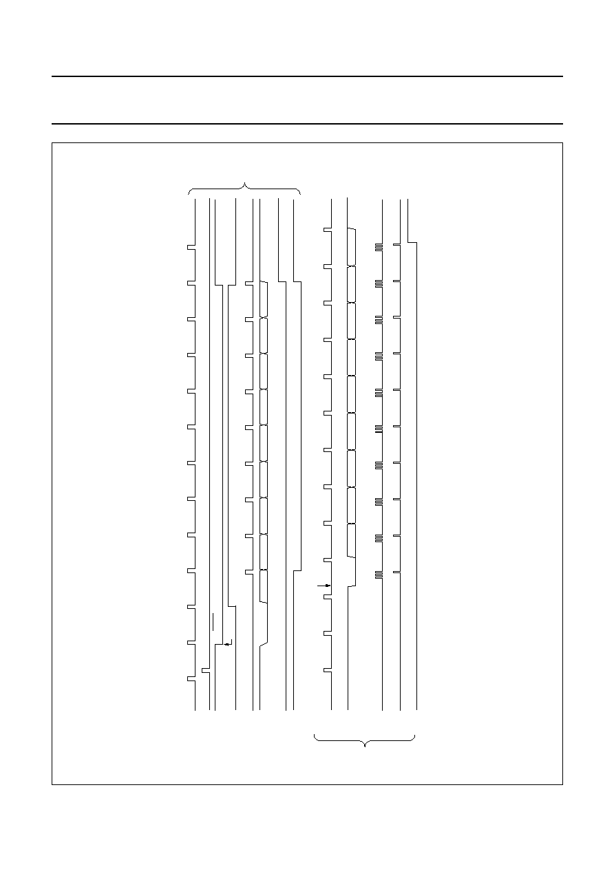
1998
Aug
26
43
Philips Semiconductors
Product specification
Low voltage 8-bit microcontroller with
6-kbyte embedded RAM
SZF2002
This text is here in white to force landscape pages to be rotated correctly when browsing through the pdf in the Acrobat reader.This text is here in
_
white to force landscape pages to be rotated correctly when browsing through the pdf in the Acrobat reader.This text is here inThis text is here in
white to force landscape pages to be rotated correctly when browsing through the pdf in the Acrobat reader. white to force landscape pages to be ...
handbook, full pagewidth
TX CLOCK
STOP BIT GEN
RX CLOCK
BIT DETECTOR SAMPLE TIME
SHIFT
MLA571
D0
D1
D2
D3
D4
D5
D6
D7
TB8
WRITE TO SBUF
SEND
DATA
SHIFT
TXD
TI
START BIT
S1P1
STOP BIT
˜
16 RESET
START BIT
RXD
D0
D1
D2
D3
D4
D5
D6
D7
STOP BIT
RI
RB8
T
R
A
N
S
M
I
T
R
E
C
E
I
V
E
Fig.22 Serial port Mode 2 timing.
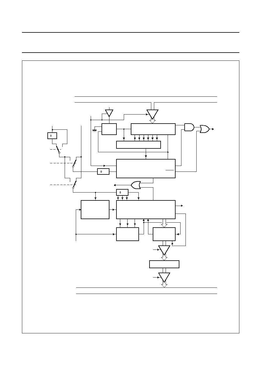
1998 Aug 26
44
Philips Semiconductors
Product specification
Low voltage 8-bit microcontroller with
6-kbyte embedded RAM
SZF2002
Fig.23 Serial port Mode 3.
handbook, full pagewidth
MGM143
START
SHIFT
DATA
T1
0
SMOD
TCLK0
1
0
1
0
1
TX CONTROL
TX CLOCK
SEND
16
serial port
interrupt
16
RX CLOCK
R1
LOAD
SBUF
SHIFT
RX CONTROL
START
HIGH-TO-LOW
TRANSITION
DETECTOR
sample
INPUT SHIFT
REGISTER
(9-BITS)
BIT
DETECTOR
S0 BUFFER
INTERNAL BUS
READ
SBUF
SHIFT
LOAD
SBUF
S0 BUFFER
ZERO DETECTOR
SHIFT
D
CL
S
Q
TB8
INTERNAL BUS
write to
SBUF
2
Timer 1
overflow
Timer 2
overflow
RXD
TXD
RCLK0
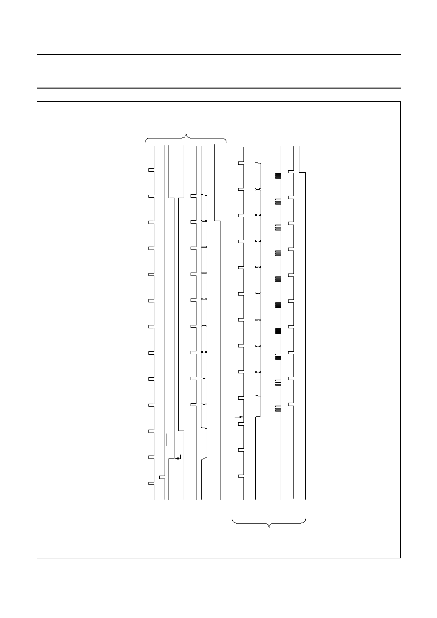
1998
Aug
26
45
Philips Semiconductors
Product specification
Low voltage 8-bit microcontroller with
6-kbyte embedded RAM
SZF2002
This text is here in white to force landscape pages to be rotated correctly when browsing through the pdf in the Acrobat reader.This text is here in
_
white to force landscape pages to be rotated correctly when browsing through the pdf in the Acrobat reader.This text is here inThis text is here in
white to force landscape pages to be rotated correctly when browsing through the pdf in the Acrobat reader. white to force landscape pages to be ...
handbook, full pagewidth
MLA573
D0
D1
D2
D3
D4
D5
D6
D7
TX CLOCK
WRITE TO SBUF
SEND
DATA
SHIFT
TXD
TI
START BIT
S1P1
STOP BIT
˜
16 RESET
START BIT
RX CLOCK
RXD
D0
D1
D2
D3
D4
D5
D6
D7
STOP BIT
BIT DETECTOR SAMPLE TIME
SHIFT
RI
TB8
TB8
T
R
A
N
S
M
I
T
R
E
C
E
I
V
E
Fig.24 Serial port Mode 3 timing.
1998 Aug 26
46
Philips Semiconductors
Product specification
Low voltage 8-bit microcontroller with
6-kbyte embedded RAM
SZF2002
18 INTERRUPT SYSTEM
External events and the real-time-driven on-chip
peripherals require service by the CPU asynchronously to
the execution of any particular section of code. To tie the
asynchronous activities of these functions to normal
program execution a multiple-source, two-priority-level,
nested interrupt system is provided. The SZF2002
acknowledges interrupt requests from fifteen sources as
follows:
∑
INT0 to INT8
∑
Timer 0, Timer 1 and Timer 2
∑
I
2
C-bus serial I/O
∑
UART
∑
ADC.
Each interrupt vectors to a separate location in program
memory for its service routine. Each source can be
individually enabled or disabled by corresponding bits in
the Interrupt Enable Registers (IEN0 and IEN1).
The priority level is selected via the Interrupt Priority
Registers (IP0 and IP1). All enabled sources can be
globally disabled or enabled. Figure 25 shows the interrupt
system.
18.1
External interrupts INT2 to INT8
Port 1 lines serve an alternative purpose as seven
additional interrupts INT2 to INT8. When enabled, each of
these lines (as well as INT0 and INT1) may wake-up the
device from the Power-down mode. Using the Interrupt
Polarity Register (IX1), each pin may be initialized to be
either active HIGH or active LOW. IRQ1 is the Interrupt
Request Flag Register. If the interrupt is enabled, each flag
will be set on an interrupt request but must be cleared by
software, i.e. via the interrupt software or when the
interrupt is disabled.
A low priority interrupt can be interrupted by a high priority
interrupt but not by another low priority interrupt. A high
priority interrupt routine can not be interrupted by any other
interrupt. If two interrupt requests of different priority levels
are received simultaneously, the request having the
highest priority level will be serviced. If interrupt requests
of the same priority level are received simultaneously an
internal polling sequence determines which request is
serviced. Thus within each priority level there is a second
priority structure determined by the polling sequence (see
Fig.25).
Port 1 interrupts are level sensitive. A Port 1 interrupt will
be recognized when a level (longer than 2 machine cycles,
HIGH or LOW, depending on the Interrupt Polarity
Register) on P1.n is made. The interrupt request is not
serviced until the next machine cycle. Figure 26 shows the
external interrupt system.
18.2
Interrupt priority
Each interrupt source can be set to either a high priority or
to a low priority. If interrupts of the same priority are
requested simultaneously, the processor will branch to the
interrupt polled first, according to Table 36.
A low priority interrupt routine can only be interrupted by a
high priority interrupt. A high priority interrupt routine can
not be interrupted.
Table 36 shows the interrupt vectors in order of priority.
The vector indicates the ROM location where the
appropriate interrupt service routine starts.
Table 36 Interrupt vectors
SYMBOL
VECTOR
ADDRESS
(HEX)
SOURCE
X0 (highest)
0003
external interrupt 0
S1
002B
I
2
C-bus port
X5
0053
external interrupt 5
T0
000B
Timer 0
T2
0033
Timer 2
X6
005B
external interrupt 6
X1
0013
external interrupt 1
X2
003B
external interrupt 2
X7
0063
external interrupt 7
T1
001B
Timer 1
X3
0043
external interrupt 3
X8
006B
external interrupt 8
SO
0023
UART
X4
004B
external interrupt 4
ADC (lowest)
0073
ADC

1998 Aug 26
47
Philips Semiconductors
Product specification
Low voltage 8-bit microcontroller with
6-kbyte embedded RAM
SZF2002
Fig.25 Interrupt system.
handbook, full pagewidth
INTERRUPT
SOURCES
REGISTERS
PRIORITY
GLOBAL
ENABLE
X0
S1
X5
T0
T2
X6
X1
X2
X7
T1
X3
X8
SO
X4
ADC
IEN0/1
IP0/1
HIGH
LOW
INTERRUPT POLLING SEQUENCE
MGD623
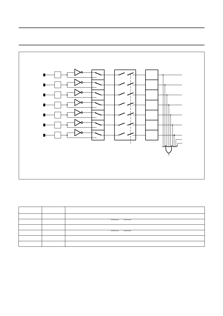
1998 Aug 26
48
Philips Semiconductors
Product specification
Low voltage 8-bit microcontroller with
6-kbyte embedded RAM
SZF2002
18.3
Interrupt related registers
The registers IEN0, IEN1, IP0, IP1, IX1 and IRQ1 are used in conjunction with the interrupt system.
Table 37 Special Function Registers related to the interrupt system
ADDRESS
REGISTER
DESCRIPTION
A8H
IEN0
Interrupt Enable Register 0
E8H
IEN1
Interrupt Enable Register 1 (INT2 to INT8)
B8H
IP0
Interrupt Priority Register 0
F8H
IP1
Interrupt Priority Register 1 (INT2 to INT8 and ADC)
E9H
IX1
Interrupt Polarity Register
C0H
IRQ1
Interrupt Request Flag Register
Fig.26 External interrupt configuration.
handbook, full pagewidth
MGM139
P1.6
P1.5
P1.4
P1.3
P1.2
P1.1
P1.0
X8
X7
X6
X5
X4
X3
X2
X1
X0
IX1
IEN1/IEN0
IRQ1
WAKE-UP
GLOBAL
ENABLE
1998 Aug 26
49
Philips Semiconductors
Product specification
Low voltage 8-bit microcontroller with
6-kbyte embedded RAM
SZF2002
18.3.1
I
NTERRUPT
E
NABLE
R
EGISTER
0 (IEN0)
Bit values: 0 = interrupt disabled; 1 = interrupt enabled.
Table 38 Interrupt Enable Register 0 (SFR address A8H)
Table 39 Description of IEN0 bits
18.3.2
I
NTERRUPT
E
NABLE
R
EGISTER
1 (IEN1)
Bit values: 0 = interrupt disabled; 1 = interrupt enabled.
Table 40 Interrupt Enable Register 1 (SFR address E8H)
Table 41 Description of IEN1 bits
7
6
5
4
3
2
1
0
EA
ET2
ES1
ES0
ET1
EX1
ET0
EX0
BIT
SYMBOL
DESCRIPTION
7
EA
General enable/disable control. If EA = 0, no interrupt is enabled; if EA = 1, any
individually enabled interrupt will be accepted.
6
ET2
enable T2 interrupt
5
ES1
enable I
2
C-bus interrupt
4
ES0
enable UART SIO interrupt
3
ET1
enable Timer 1 interrupt (T1)
2
EX1
enable external interrupt 1
1
ET0
enable Timer 0 interrupt (T0)
0
EX0
enable external interrupt 0
7
6
5
4
3
2
1
0
EAD
EX8
EX7
EX6
EX5
EX4
EX3
EX2
BIT
SYMBOL
DESCRIPTION
7
EAD
enable ADC interrupt (external interrupt 9)
6
EX8
enable external interrupt 8
5
EX7
enable external interrupt 7
4
EX6
enable external interrupt 6
3
EX5
enable external interrupt 5
2
EX4
enable external interrupt 4
1
EX3
enable external interrupt 3
0
EX2
enable external interrupt 2
1998 Aug 26
50
Philips Semiconductors
Product specification
Low voltage 8-bit microcontroller with
6-kbyte embedded RAM
SZF2002
18.3.3
I
NTERRUPT
P
RIORITY
R
EGISTER
0 (IP0)
Bit values: 0 = low priority; 1 = high priority.
Table 42 Interrupt Priority Register 0 (SFR address B8H)
Table 43 Description of IP0 bits
18.3.4
I
NTERRUPT
P
RIORITY
R
EGISTER
1 (IP1)
Bit values: 0 = low priority; 1 = high priority.
Table 44 Interrupt Priority Register 1 (SFR address F8H)
Table 45 Description of IP1 bits
7
6
5
4
3
2
1
0
-
PT2
PS1
PS0
PT1
PX1
PT0
PX0
BIT
SYMBOL
DESCRIPTION
7
-
reserved
6
PT2
Timer 2 interrupt priority level
5
PS1
I
2
C-bus interrupt priority level
4
PS0
UART SIO interrupt priority level
3
PT1
Timer 1 interrupt priority level
2
PX1
external interrupt 1 priority level
1
PT0
Timer 0 interrupt priority level
0
PX0
external interrupt 0 priority level
7
6
5
4
3
2
1
0
PADC
PX8
PX7
PX6
PX5
PX4
PX3
PX2
BIT
SYMBOL
DESCRIPTION
7
PADC
ADC interrupt priority level
6
PX8
external interrupt 8 priority level
5
PX7
external interrupt 7 priority level
4
PX6
external interrupt 6 priority level
3
PX5
external interrupt 5 priority level
2
PX4
external interrupt 4 priority level
1
PX3
external interrupt 3 priority level
0
PX2
external interrupt 2 priority level
1998 Aug 26
51
Philips Semiconductors
Product specification
Low voltage 8-bit microcontroller with
6-kbyte embedded RAM
SZF2002
18.3.5
I
NTERRUPT
P
OLARITY
R
EGISTER
(IX1)
Writing either a logic 1 or logic 0 to any Interrupt Polarity Register bit sets the polarity level of the corresponding external
interrupt to an active HIGH or active LOW respectively.
Table 46 Interrupt Polarity Register (SFR address E9H)
Table 47 Description of IX1 bits
18.3.6
I
NTERRUPT
R
EQUEST
F
LAG
R
EGISTER
(IRQ1)
Table 48 Interrupt Request Flag Register (SFR address C0H)
Table 49 Description of IRQ1 bits
7
6
5
4
3
2
1
0
-
IL8
IL7
IL6
IL5
IL4
IL3
IL2
BIT
SYMBOL
DESCRIPTION
7
-
reserved
6
IL8
external interrupt 8 polarity level
5
IL7
external interrupt 7 polarity level
4
IL6
external interrupt 6 polarity level
3
IL5
external interrupt 5 polarity level
2
IL4
external interrupt 4 polarity level
1
IL3
external interrupt 3 polarity level
0
IL2
external interrupt 2 polarity level
7
6
5
4
3
2
1
0
-
IQ8
IQ7
IQ6
IQ5
IQ4
IQ3
IQ2
BIT
SYMBOL
DESCRIPTION
7
-
reserved
6
IQ8
external interrupt 8 request flag
5
IQ7
external interrupt 7 request flag
4
IQ6
external interrupt 6 request flag
3
IQ5
external interrupt 5 request flag
2
IQ4
external interrupt 4 request flag
1
IQ3
external interrupt 3 request flag
0
IQ2
external interrupt 2 request flag

1998 Aug 26
52
Philips Semiconductors
Product specification
Low voltage 8-bit microcontroller with
6-kbyte embedded RAM
SZF2002
19 CLOCK CIRCUITRY
The SZF2002 is clocked with an external digital clock.
The input must be driven with a digital square wave.
Note that the duty cycle influences the timing to the
external components, since both the positive and negative
clock edges are used.
20 RESET
To initialize the SZF2002 a reset is performed by either of
two methods:
∑
Applying an external signal to the RST pin
∑
Watchdog Timer overflow.
20.1
External reset using the RST pin
The reset input for the SZF2002 is RST. A reset is
accomplished by holding the RST pin HIGH for at least two
machine cycles (12 clock periods) while the clock is
running. The CPU responds by executing an internal reset.
Port pins adopt their reset state immediately after the RST
goes HIGH. During reset, WE and OE, and CE are held
HIGH.
The external reset is asynchronous to the internal clock.
The RST pin is sampled during state 5, phase 2 of every
machine cycle. After a HIGH is detected at the RST pin, an
internal reset is repeated until RST goes LOW. The reset
circuitry is also affected by the Watchdog Timer as
described in Section 12.5. The internal RAM is not
affected by reset. When V
DD
is turned on, the RAM
contents are indeterminate.
20.2
Power-on-reset
The device contains on-chip circuitry which switches the
port pins to HIGH as soon as RST goes HIGH. The user
must ensure that the RST pin is held HIGH until the
external clock has stabilised. When RST goes LOW a
further 3 cycles elapse before execution starts.

1998 Aug 26
53
Philips Semiconductors
Product specification
Low voltage 8-bit microcontroller with
6-kbyte embedded RAM
SZF2002
21 SPECIAL FUNCTION REGISTERS OVERVIEW
ADDRESS
(HEX)
NAME
RESET VALUE
(B)
FUNCTION
FF
T3
0000 0000
Watchdog Timer
FE
PWMP
(1)
0000 0000
Prescaler Frequency Control Register
FC
PWM
(1)
0000 0000
Pulse Width Register
F8
IP1
(1)(2)
0000 0000
Interrupt Priority Register 1 (INT2 to INT8 and ADC)
F7
WDTKEY
(1)
0000 0000
Watchdog Timer enable
F0
B
(2)
0000 0000
B Register
E9
IX1
(1)
X
000 0000
Interrupt Polarity Register 1
E8
IEN1
(1)(2)
0000 0000
Interrupt Enable Register 1
E0
ACC
(2)
0000 0000
Accumulator
DB
S1ADR
(1)
0000 0000
I
2
C-bus Slave Address Register
DA
S1DAT
(1)
0000 0000
I
2
C-bus Data Shift Register
D9
S1STA
(1)
1111 1000
I
2
C-bus Serial Status Register
D8
S1CON
(1)(2)
0000 0000
I
2
C-bus Serial Control Register
D0
PSW
(2)
0000 0000
Program Status Word
CD
TH2
(1)
0000 0000
Timer 2 High byte
CC
TL2
(1)
0000 0000
Timer 2 Low byte
CB
RCAP2H
(1)
0000 0000
Timer 2 Reload/Capture Register High byte
CA
RCAP2L
(1)
0000 0000
Timer 2 Reload/Capture Register Low byte
C9
T2MOD
(1)
XX
00
X
000
Timer/Counter 2 mode control
C8
T2CON
(1)(2)
0000 0000
Timer/Counter 2 Control Register
C5
ADCH
(1)
1111 1111
ADC Result Register
C4
ADCON
(1)
X
000 0000
ADC Control Register
C1
P4
(1)
1111 1111
Digital I/O Port Register 4
C0
IRQ1
(1)(2)
X
000 0000
Interrupt Request Flag Register
B8
IP0
(2)
X
000 0000
Interrupt Priority Register 0
B0
P3
(2)
1111 1111
Digital I/O Port Register 3
A8
IEN0
(2)
0000 0000
Interrupt Enable Register 0
A0
P2
(2)
1111 1111
Digital I/O Port Register 2
1998 Aug 26
54
Philips Semiconductors
Product specification
Low voltage 8-bit microcontroller with
6-kbyte embedded RAM
SZF2002
Notes
1. SZF2002 specific SFRs.
2. Bit addressed register.
99
S0BUF
XXXX XXXX
Serial Data Buffer Register 0
98
S0CON
(2)
0000 0000
Serial Port Control Register 0
91
ROMBANK
(1)
XXXX X
000
ROM bank Selection Register
90
P1
(2)
1111 1111
Digital I/O Port Register 1
8D
TH1
0000 0000
Timer 1 High byte
8C
TH0
0000 0000
Timer 0 High byte
8B
TL1
0000 0000
Timer 1 Low byte
8A
TL0
0000 0000
Timer 0 Low byte
89
TMOD
0000 0000
Timer 0 and 1 Mode Control Register
88
TCON
(2)
0000 0000
Timer 0 and 1 Control/External Interrupt Control Register
87
PCON
0000 0000
Power Control Register
83
DPH
0000 0000
Data Pointer High byte
82
DPL
0000 0000
Data Pointer Low byte
81
SP
0000 0111
Stack Pointer
80
P0
(2)
1111 1111
Digital I/O Port Register 0
ADDRESS
(HEX)
NAME
RESET VALUE
(B)
FUNCTION

1998 Aug 26
55
Philips Semiconductors
Product specification
Low voltage 8-bit microcontroller with
6-kbyte embedded RAM
SZF2002
22 DEBUGGING SUPPORT
For software development the SZF2002 is made
compatible with the Nohau 80C51 In-Circuit Emulator
(ICE).
22.1
Recommended equipment
1. Nohau EMUL51-PC/EA768-BSW-42 42 MHz,
768-kbyte emulator memory board.
2. Nohau EMUL51-PC/ATR64-33, 33 MHz, 64-kbyte
advanced trace memory board.
3. Nohau EMUL51-PC/POD-C32HF-42, external
memory mode pod for a.o. 80C51/80C32.
22.2
Connecting the pod
The Nohau In-Circuit Emulator requires the following
80C51 pins: P0.0 to P0.7, P2.0 to P2.7, ALE, PSEN, RD,
WR, EA and RST.
When setting the SZF2002 in Debug mode (force DEBUG
HIGH), these signals become available on the pins as
described in Section 7.2
The connection between the SZF2002 and the emulator is
shown in Fig.27.
For emulation the Target board must be configured with
the SZF2002 mounted, but without external Flash and
RAM, or disabled by disconnecting the OE.
On the Target board a 40-pin connector is required that
has all the necessary 80C51 signals (Port 0, Port 2,
PSEN, ALE, EA, RST, V
DD
and V
SS
). The 16 port pins are
optional. The three banking bits are not standard 80C51
signals and are not available at the DIL40
80C51-connector of the pod. These three bits must be
connected via three separate wires to the signals BS0
(LSB), BS1 and BS2 (MSB) on the pod.
The emulator pod has a DIL40 socket for the 80C51
processor (on the upper side). By connecting the 40-pin
connector to this socket the emulator will approach the
SZF2002 as if it were a 80C51. The connector on the lower
side of the pod is not used. The emulator acts as a memory
emulator.
22.3
Powering the pod
Because the SZF2002 is a 3 V circuit, the ICE pod must be
powered by the target (supply from PC is not possible, see
documentation for EMUL51-PC/POD-C32HF-42).
Therefore, V
DD
and V
SS
for the SZF2002 are also required.
The clock signal is not required on the pod.
The digital power V
DD
has to be connected to the pod.
The ground of the pod must be connected to the ground of
the target board via the black gnd-wire soldered to the pod
Because the target supplies the pod the following
power-up/power-down sequence is required:
1. Switch on target.
2. Switch on PC.
3. Switch off target.
When using 3 V power from the target, note that the pod
will drive the inputs up to 3.5 V. Some current will also flow
through the V
DD
connection to the target. If the emulator is
used together with an I
2
C-bus interface to a PC or together
with an RS232-connection, use 3.3 V power for the target.
This will reduce noise and disturbance on all input and
output signals. In practice, it is seen that this will result in a
more robust communication between the SZF2002 and
Nohau.
Both I
2
C-bus pins (SDA and SCL) need an external pull-up
resistor.
22.4
Bank switching support
If bank switching is required, the in-circuit emulator also
needs the TRUE_A15 and the three banking bits
A15 to A17.
16 port pins (selection of Ports 3 and 4) can also be
connected to the emulator pod, however this is not
necessary. When connected, the state of these ports can
be traced.
To set up the banking configuration the BM jumpers on the
emulator board have to be set. The following set-up is
recommended:
1. Jumper BM3 is out.
2. Jumper BM2 is out.
3. Jumper BM1is don't care.
4. Jumper BM0 is in.
22.5
Software recommendations
The Keil/Franklin assembler and banked linker is well
suited for use with the Nohau ICE (especially for banking
configurations).
The Nohau ICE communicates with the SZF2002 using
MOVX instructions. Therefore, all MOVX instructions must
be forced to access off-chip memory instead of internal
AUX RAM by setting the ARD bit of the SFR PCON.
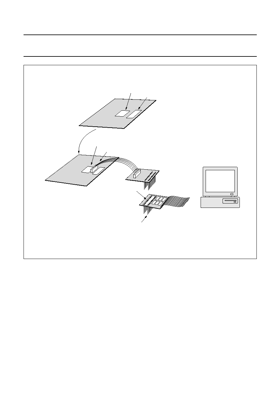
1998 Aug 26
56
Philips Semiconductors
Product specification
Low voltage 8-bit microcontroller with
6-kbyte embedded RAM
SZF2002
Fig.27 In-circuit emulation.
handbook, full pagewidth
MBK834
SZF2002
Flash
SZF2002
connector
target PCB
(Flash is disabled,
doesn't need to
be mounted)
adapter PCB
socket for
target
processor
this socket not used
flat cable to PC
type 31A POD
NOHAU emulator
PC with emulator cards
1998 Aug 26
57
Philips Semiconductors
Product specification
Low voltage 8-bit microcontroller with
6-kbyte embedded RAM
SZF2002
23 INSTRUCTION SET
The SZF2002 uses a powerful instruction set which optimizes byte efficiency and execution speed. Assigned opcodes
add new high-power operation and permit new addressing modes. The instruction set consists of 49 single-byte,
46 two-byte and 16 three-byte instructions. When using a 12 MHz clock, 64 instructions execute in 0.5
µ
s and
45 instructions execute in 1
µ
s. Multiply and divide instructions execute in 2
µ
s.
For the description of the Data Addressing modes and Hexadecimal opcode cross-reference see Table 54.
Table 50 Instruction set description: Arithmetic operations
MNEMONIC
DESCRIPTION
BYTES
CYCLES
OPCODE
(HEX)
Arithmetic operations
ADD
A,Rr
add register to A
1
1
2*
ADD
A,direct
add direct byte to A
2
1
25
ADD
A,@Ri
add indirect RAM to A
1
1
26 and 27
ADD
A,#data
add immediate data to A
2
1
24
ADDC
A,Rr
add register to A with carry flag
1
1
3*
ADDC
A,direct
add direct byte to A with carry flag
2
1
35
ADDC
A,@Ri
add indirect RAM to A with carry flag
1
1
36 and 37
ADDC
A,#data
add immediate data to A with carry flag
2
1
34
SUBB
A,Rr
subtract register from A with borrow
1
1
9*
SUBB
A,direct
subtract direct byte from A with borrow
2
1
95
SUBB
A,@Ri
subtract indirect RAM from A with borrow
1
1
96 and 97
SUBB
A,#data
subtract immediate data from A with borrow
2
1
94
INC
A
increment A
1
1
04
INC
Rr
increment register
1
1
0*
INC
direct
increment direct byte
2
1
05
INC
@Ri
increment indirect RAM
1
1
06 and 07
DEC
A
decrement A
1
1
14
DEC
Rr
decrement register
1
1
1*
DEC
direct
decrement direct byte
2
1
15
DEC
@Ri
decrement indirect RAM
1
1
16 and 17
INC
DPTR
increment data pointer
1
2
A3
MUL
AB
multiply A and B
1
4
A4
DIV
AB
divide A by B
1
4
84
DA
A
decimal adjust A
1
1
D4

1998 Aug 26
58
Philips Semiconductors
Product specification
Low voltage 8-bit microcontroller with
6-kbyte embedded RAM
SZF2002
Table 51 Instruction set description: Logic operations
MNEMONIC
DESCRIPTION
BYTES
CYCLES
OPCODE
(HEX)
Logic operations
ANL
A,Rr
AND register to A
1
1
5*
ANL
A,direct
AND direct byte to A
2
1
55
ANL
A,@Ri
AND indirect RAM to A
1
1
56 and 57
ANL
A,#data
AND immediate data to A
2
1
54
ANL
direct,A
AND A to direct byte
2
1
52
ANL
direct,#data
AND immediate data to direct byte
3
2
53
ORL
A,Rr
OR register to A
1
1
4*
ORL
A,direct
OR direct byte to A
2
1
45
ORL
A,@Ri
OR indirect RAM to A
1
1
46 and 47
ORL
A,#data
OR immediate data to A
2
1
44
ORL
direct,A
OR A to direct byte
2
1
42
ORL
direct,#data
OR immediate data to direct byte
3
2
43
XRL
A,Rr
exclusive-OR register to A
1
1
6*
XRL
A,direct
exclusive-OR direct byte to A
2
1
65
XRL
A,@Ri
exclusive-OR indirect RAM to A
1
1
66 and 67
XRL
A,#data
exclusive-OR immediate data to A
2
1
64
XRL
direct,A
exclusive-OR A to direct byte
2
1
62
XRL
direct,#data
exclusive-OR immediate data to direct byte
3
2
63
CLR
A
clear A
1
1
E4
CPL
A
complement A
1
1
F4
RL
A
rotate A left
1
1
23
RLC
A
rotate A left through the carry flag
1
1
33
RR
A
rotate A right
1
1
03
RRC
A
rotate A right through the carry flag
1
1
13
SWAP
A
swap nibbles within A
1
1
C4

1998 Aug 26
59
Philips Semiconductors
Product specification
Low voltage 8-bit microcontroller with
6-kbyte embedded RAM
SZF2002
Table 52 Instruction set description: Data transfer
Note
1. MOV A,ACC is not permitted.
MNEMONIC
DESCRIPTION
BYTES
CYCLES
OPCODE
(HEX)
Data transfer
MOV
A,Rr
move register to A
1
1
E*
MOV
A,direct (note 1) move direct byte to A
2
1
E5
MOV
A,@Ri
move indirect RAM to A
1
1
E6 and E7
MOV
A,#data
move immediate data to A
2
1
74
MOV
Rr,A
move A to register
1
1
F*
MOV
Rr,direct
move direct byte to register
2
2
A*
MOV
Rr,#data
move immediate data to register
2
1
7*
MOV
direct,A
move A to direct byte
2
1
F5
MOV
direct,Rr
move register to direct byte
2
2
8*
MOV
direct,direct
move direct byte to direct
3
2
85
MOV
direct,@Ri
move indirect RAM to direct byte
2
2
86 and 87
MOV
direct,#data
move immediate data to direct byte
3
2
75
MOV
@Ri,A
move A to indirect RAM
1
1
F6 and F7
MOV
@Ri,direct
move direct byte to indirect RAM
2
2
A6 and A7
MOV
@Ri,#data
move immediate data to indirect RAM
2
1
76 and 77
MOV
DPTR,#data 16
load data pointer with a 16-bit constant
3
2
90
MOVC
A,@A+DPTR
move code byte relative to DPTR to A
1
2
93
MOVC
A,@A+PC
move code byte relative to PC to A
1
2
83
MOVX
A,@Ri
move external RAM (8-bit address) to A
1
2
E2 and E3
MOVX
A,@DPTR
move external RAM (16-bit address) to A
1
2
E0
MOVX
@Ri,A
move A to external RAM (8-bit address)
1
2
F2 and F3
MOVX
@DPTR,A
move A to external RAM (16-bit address)
1
2
F0
PUSH
direct
push direct byte onto stack
2
2
C0
POP
direct
pop direct byte from stack
2
2
D0
XCH
A,Rr
exchange register with A
1
1
C*
XCH
A,direct
exchange direct byte with A
2
1
C5
XCH
A,@Ri
exchange indirect RAM with A
1
1
C6 and C7
XCHD
A,@Ri
exchange LOW-order digit indirect RAM with A
1
1
D6 and D7
1998 Aug 26
60
Philips Semiconductors
Product specification
Low voltage 8-bit microcontroller with
6-kbyte embedded RAM
SZF2002
Table 53 Instruction set description: Boolean variable manipulation and Program and machine control
MNEMONIC
DESCRIPTION
BYTES
CYCLES
OPCODE
(HEX)
Boolean variable manipulation
CLR
C
clear carry flag
1
1
C3
CLR
bit
clear direct bit
2
1
C2
SETB
C
set carry flag
1
1
D3
SETB
bit
set direct bit
2
1
D2
CPL
C
complement carry flag
1
1
B3
CPL
bit
complement direct bit
2
1
B2
ANL
C,bit
AND direct bit to carry flag
2
2
82
ANL
C,/bit
AND complement of direct bit to carry flag
2
2
B0
ORL
C,bit
OR direct bit to carry flag
2
2
72
ORL
C,/bit
OR complement of direct bit to carry flag
2
2
A0
MOV
C,bit
move direct bit to carry flag
2
1
A2
MOV
bit,C
move carry flag to direct bit
2
2
92
Program and machine control
ACALL
addr11
absolute subroutine call
2
2
∑
1
LCALL
addr16
long subroutine call
3
2
12
RET
return from subroutine
1
2
22
RETI
return from interrupt
1
2
32
AJMP
addr11
absolute jump
2
2
1
LJMP
addr16
long jump
3
2
02
SJMP
rel
short jump (relative address)
2
2
80
JMP
@A+DPTR
jump indirect relative to the DPTR
1
2
73
JZ
rel
jump if A is zero
2
2
60
JNZ
rel
jump if A is not zero
2
2
70
JC
rel
jump if carry flag is set
2
2
40
JNC
rel
jump if carry flag is not set
2
2
50
JB
bit,rel
jump if direct bit is set
3
2
20
JNB
bit,rel
jump if direct bit is not set
3
2
30
JBC
bit,rel
jump if direct bit is set and clear bit
3
2
10
CJNE
A,direct,rel
compare direct to A and jump if not equal
3
2
B5
CJNE
A,#data,rel
compare immediate to A and jump if not equal
3
2
B4
CJNE
Rr,#data,rel
compare immediate to register and jump if not equal
3
2
B*
CJNE
@Ri,#data,rel compare immediate to indirect and jump if not equal
3
2
B6 and B7
DJNZ
Rr,rel
decrement register and jump if not zero
2
2
D*
DJNZ
direct,rel
decrement direct and jump if not zero
3
2
D5
NOP
no operation
1
1
00

1998 Aug 26
61
Philips Semiconductors
Product specification
Low voltage 8-bit microcontroller with
6-kbyte embedded RAM
SZF2002
Table 54 Description of the mnemonics in the Instruction set
MNEMONIC
DESCRIPTION
Data addressing modes
Rr
Working registers R0 to R7.
direct
128 internal RAM locations and any special function register (SFR).
@Ri
Indirect internal RAM location addressed by register R0 or R1 of the actual register bank.
#data
8-bit constant included in instruction.
#data 16
16-bit constant included as bytes 2 and 3 of instruction.
bit
Direct addressed bit in internal RAM or SFR.
addr16
16-bit destination address. Used by LCALL and LJMP. The branch will be anywhere within the
64 kbytes program memory address space.
addr11
111-bit destination address. Used by ACALL and AJMP. The branch will be within the same 2 kbytes
page of program memory as the first byte of the following instruction.
rel
Signed (two's complement) 8-bit offset byte. Used by SJMP and all conditional jumps. Range is
-
128 to + 127 bytes relative to first byte of the following instruction.
Hexadecimal opcode cross-reference
*
8, 9, A, B, C, D, E and F.
∑
1, 3, 5, 7, 9, B, D and F.
0, 2, 4, 6, 8, A, C and E.

1998
Aug
26
62
Philips Semiconductors
Product specification
Low voltage 8-bit microcontroller with
6-kbyte embedded RAM
SZF2002
This text is here in white to force landscape pages to be rotated correctly when browsing through the pdf in the Acrobat reader.This text is here in
_
white to force landscape pages to be rotated correctly when browsing through the pdf in the Acrobat reader.This text is here inThis text is here in
white to force landscape pages to be rotated correctly when browsing through the pdf in the Acrobat reader. white to force landscape pages to be ...
Table 55 Instruction map
Note
1. MOV A, ACC is not a valid instruction.
First hexadecimal character of opcode
Second hexadecimal character of opcode
0
1
2
3
4
5
6
7
8
9
A B C D E
F
0
NOP
AJMP
addr11
LJMP
addr16
RR
A
INC
A
INC
direct
INC @Ri
INC Rr
0
1
0
1
2
3
4
5
6
7
1
JBC
bit,rel
ACALL
addr11
LCALL
addr16
RRC
A
DEC
A
DEC
direct
DEC @Ri
DEC Rr
0
1
0
1
2
3
4
5
6
7
2
JB
bit,rel
AJMP
addr11
RET
RL
A
ADD
A,#data
ADD
A,direct
ADD A,@Ri
ADD A,Rr
0
1
0
1
2
3
4
5
6
7
3
JNB
bit,rel
ACALL
addr11
RETI
RLC
A
ADDC
A,#data
ADDC
A,direct
ADDC A,@Ri
ADDC A,Rr
0
1
0
1
2
3
4
5
6
7
4
JC
rel
AJMP
addr11
ORL
direct,A
ORL
direct,#data
ORL
A,#data
ORL
A,direct
ORL A,@Ri
ORL A,Rr
0
1
0
1
2
3
4
5
6
7
5
JNC
rel
ACALL
addr11
ANL
direct,A
ANL
direct,#data
ANL
A,#data
ANL
A,direct
ANL A,@Ri
ANL A,Rr
0
1
0
1
2
3
4
5
6
7
6
JZ
rel
AJMP
addr11
XRL
direct,A
XRL
direct,#data
XRL
A,#data
XRL
A,direct
XRL A,@Ri
XRL A,Rr
0
1
0
1
2
3
4
5
6
7
7
JNZ
rel
ACALL
addr11
ORL
C,bit
JMP
@A+DPTR
MOV
A,#data
MOV
direct,#data
MOV @Ri,#data
MOV Rr,#data
0
1
0
1
2
3
4
5
6
7
8
SJMP
rel
AJMP
addr11
ANL
C,bit
MOVC
A,@A+PC
DIV
AB
MOV
direct,direct
MOV direct,@Ri
MOV direct,Rr
0
1
0
1
2
3
4
5
6
7
9
MOV
DTPR,#data16
ACALL
addr11
MOV
bit,C
MOVC
A,@A+DPTR
SUBB
A,#data
SUBB
A,direct
SUBB A,@Ri
SUB A,Rr
0
1
0
1
2
3
4
5
6
7
A
ORL
C,/bit
AJMP
addr11
MOV
bit,C
INC
DPTR
MUL
AB
MOV @Ri,direct
MOV Rr,direct
0
1
0
1
2
3
4
5
6
7
B
ANL
C,/bit
ACALL
addr11
CPL
bit
CPL
C
CJNE
A,#data,rel
CJNE
A,direct,rel
CJNE @Ri,#data,rel
CJNE Rr,#data,rel
0
1
0
1
2
3
4
5
6
7
C
PUSH
direct
AJMP
addr11
CLR
bit
CLR
C
SWAP
A
XCH
A,direct
XCH A,@Ri
XCH A,Rr
0
1
0
1
2
3
4
5
6
7
D
POP
direct
ACALL
addr11
SETB
bit
SETB
C
DA
A
DJNZ
direct,rel
XCHD A,@Ri
DJNZ Rr,rel
0
1
0
1
2
3
4
5
6
7
E
MOVX
A,@DTPR
AJMP
addr11
MOVX A,@Ri
CLR
A
MOV
A,direct
(1)
MOV A,@Ri
MOV A,Rr
0
1
0
1
0
1
2
3
4
5
6
7
F
MOVX
@DTPR,A
ACALL
addr11
MOVX @Ri,A
CPL
A
MOV
direct,A
MOV @Ri,A
MOV Rr,A
0
1
0
1
0
1
2
3
4
5
6
7
1998 Aug 26
63
Philips Semiconductors
Product specification
Low voltage 8-bit microcontroller with
6-kbyte embedded RAM
SZF2002
24 LIMITING VALUES
In accordance with the Absolute Maximum Rating System (IEC 134).
25 DC CHARACTERISTICS
V
DD
= 2.7 to 3.3 V; V
SS
= 0 V; T
amb
=
-
40 to +85
∞
C; see note 1; all voltages are with respect to V
SS
; unless otherwise
specified.
Notes to the DC characteristics
1. Loading ports and busses may cause spurious noise pulses to be superimposed on the output voltage.
SYMBOL
PARAMETER
MIN.
MAX.
UNIT
V
DD
supply voltage
-
0.5
+5
V
V
I
input voltage on any pin with respect to ground (V
SS
)
-
0.5
V
DD
+ 0.5
V
I
I
and I
O
DC current on any input or output
-
tbf
mA
P
tot
total power dissipation
-
500
mW
T
stg
storage temperature
-
65
+150
∞
C
T
amb
operating ambient temperature
-
40
+85
∞
C
T
j
operating junction temperature
-
40
+125
∞
C
SYMBOL
PARAMETER
CONDITIONS
MIN.
TYP.
MAX.
UNIT
Supply
V
DD
operating supply voltage
2.7
-
3.3
V
I
DD
operating supply current
V
DD
= 3.0 V; f
CLK
= 8 MHz; note 2
-
-
9
mA
V
DD
= 3.0 V; f
CLK
= 3.58 MHz;
note 2
-
-
2.5
mA
I
DD(idle)
Idle mode supply current
V
DD
= 3.0 V; f
CLK
= 8 MHz; note 3
-
-
5.0
mA
V
DD
= 3.0 V; f
CLK
= 3.58 MHz;
note 3
-
-
1.5
mA
I
DD(pd)
Power-down mode current
V
DD
= 3.0 V; T
amb
= 25
∞
C; note 4
-
-
10
µ
A
Inputs (note 5)
V
IL
LOW-level input voltage
V
SS
-
0.2V
DD
V
V
IH
HIGH-level input voltage
0.8V
DD
-
V
DD
V
I
LI
input leakage current
V
SS
< V
i
< V
DD
; V
DD
= 3.0 V;
T
amb
= 25
∞
C
-
1
-
+1
µ
A
I
IL
input pull-up current
Input = HIGH
-
-
tbf
µ
A
Outputs
V
OL
LOW-level output voltage
-
-
0.4
V
V
OH
HIGH-level output voltage
V
DD
-
0.4
-
-
V
I
OL
LOW-level output current
4.0
-
-
mA
I
OH
HIGH-level output current
-
4.0
-
-
mA
R
RST
RST pull-down resistor
120
160
250
k
Analog inputs
V
DDA
analog supply voltage
V
DD
-
0.5
-
V
DD
+ 0.5 V
I
DDA
supply current operating
V
DDA
= 3.0 V; f
CLK
= 8 MHz; note 2
-
-
0.5
mA
1998 Aug 26
64
Philips Semiconductors
Product specification
Low voltage 8-bit microcontroller with
6-kbyte embedded RAM
SZF2002
2. The operating supply current is measured with all output pins disconnected; CLK driven with t
r
= t
f
= 10 ns;
V
IL
= V
SS
; V
IH
= V
DD
; EA = RST = Port 0 = V
DD
.
3. The Idle mode supply current is measured with all output pins disconnected; CLK driven with t
r
= t
f
= 10 ns; V
IL
= V
SS
;
V
IH
= V
DD
; EA = Port 0 = V
DD
.
4. The power-down current is measured with all output pins disconnected; CLK connected to V
SS
; EA = Port 0 = V
DD
;
RST = V
SS
.
5. The input threshold voltage of P1.6/SCL and P1.7/SDA meet the I
2
C-bus specification. Therefore, an input voltage
below 0.3V
DD
will be recognized as a logic 0 and an input voltage above 0.7V
DD
will be recognized as a logic 1.
26 ADC CHARACTERISTICS
Notes
1. All ADC inputs require an external divide-by-2 voltage divider.
2. Gain error: the maximum difference between actual and ideal slope.
3. Zero-offset error: the difference between the actual and ideal input voltage corresponding to the first actual code
transition.
4. Differential non-linearity: the difference between the actual and ideal code widths.
5. Integral non-linearity: maximum deviation from straight line.
6. Channel-to-channel matching: the difference between corresponding code transitions of actual characteristics taken
from different channels under the same temperature, voltage and frequency conditions. Not tested, but verified on
sampling basis.
SYMBOL
PARAMETER
CONDITIONS
MIN.
TYP.
MAX.
UNIT
V
IN(ADC)
ADC input voltage
note 1
V
SSA
-
0.5V
DDA
V
V
DDA
analog supply voltage
V
DD
-
0.5
-
V
DD
+ 0.5
V
I
DDA
supply current operating
V
DDA
= 3.0 V; f
clk
= 8 MHz
-
-
0.5
mA
C
AIN
analog on-chip input capacitance
-
-
2
pF
R
AIN
analog on-chip input impedance
10
-
-
M
G
e
Gain error; note 2
-
1
-
+1
%
OS
e
zero-offset error; note 3
-
1
-
+1
LSB
DNL
differential non-linearity; note 4
-
0.5
-
+0.5
LSB
INL
Integral non-linearity; note 5
-
1
-
+1
LSB
M
ctc
channel-to-channel matching;
note 6
-
-
±
1
/
2
LSB
V
I(slope)
input voltage slope
f
clk
= 8 MHz
-
0.15
-
+0.15
V/ms
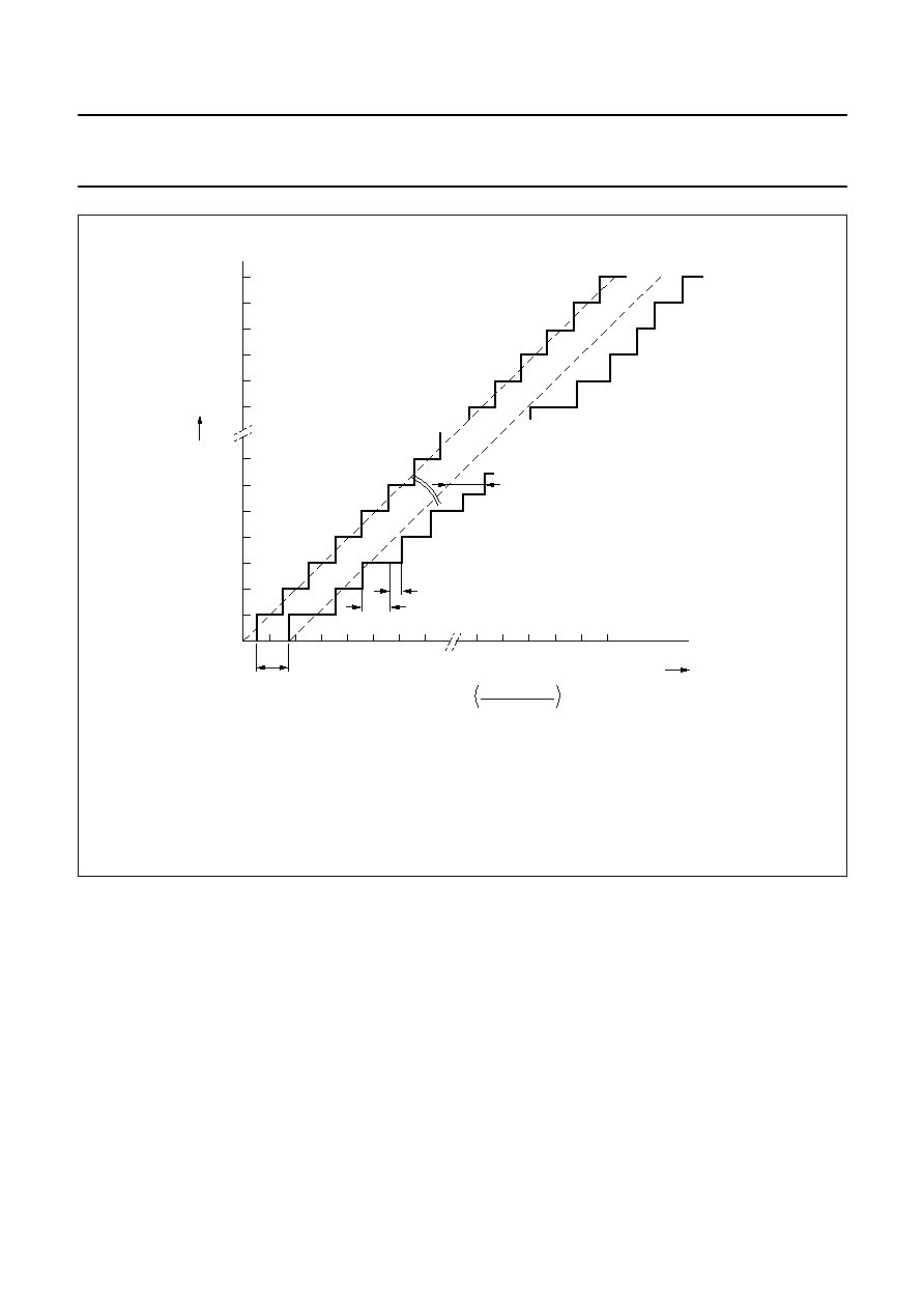
1998 Aug 26
65
Philips Semiconductors
Product specification
Low voltage 8-bit microcontroller with
6-kbyte embedded RAM
SZF2002
Fig.28 Analog-to-Digital conversion characteristics.
(1) The ideal transfer curve.
(2) The actual transfer curve.
(3) Differential non-linearity (DNL).
(4) Integral non-linearity (INL).
(5) Gain error (G
e
).
handbook, full pagewidth
MGM135
1
2
3
4
5
6
7
250 251 252 253 254 255
0
1
2
3
4
5
250
251
252
253
254
255
VIN(A)(LSBideal)
code
out
zero offset
error
1 LSB (ideal)
(3)
(5)
(4)
(1)
(2)
1LSB =
VDDA
-
VSSA
255
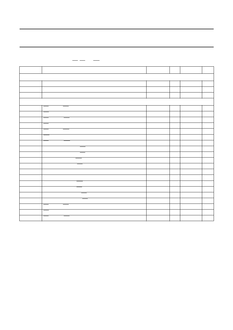
1998 Aug 26
66
Philips Semiconductors
Product specification
Low voltage 8-bit microcontroller with
6-kbyte embedded RAM
SZF2002
27 AC CHARACTERISTICS
Table 56 Timing with respect to CE, OE and WE
SYMBOL
PARAMETER
MIN.
TYP
MAX.
UNIT
General (see Fig.29)
t
XCLKH
XCLK HIGH time
31.25
-
-
ns
t
XCLKL
XCLK LOW time
31.25
-
-
ns
T
cy(XCLK)
XCLK cycle time
62.5
-
-
ns
Memory Access (Figs 29 and 30)
t
(CEL-OEL)1
CE LOW to OE LOW (data cycle)
-
-
1
/
2
t
CLK
+ 3
ns
t
(OEL)1
OE LOW time (data cycle)
-
-
7
/
2
t
CLK
+ 7
ns
t
(CEH-OEH)1
CE HIGH to OE HIGH (data cycle)
0
-
12
ns
t
(CEL)1
CE LOW time (data cycle)
-
-
4t
CLK
ns
t
(CEL-WEL)1
CE LOW to WE LOW (data cycle)
-
-
1
/
2
t
CLK
+ 5
ns
t
(WEL)1
WE LOW time (data cycle)
-
-
7
/
2
t
CLK
+ 8
ns
t
(CEH-WEH)1
CE HIGH to WE HIGH (data cycle)
0
-
13
ns
t
su(OE-D)2
Data set-up time from OE (data read cycle)
-
-
3t
CLK
-
18
ns
t
su(CEL-D)2
Data set-up time from CE LOW (data read cycle)
-
-
7
/
2
t
CLK
-
18
ns
t
su(D-WEL)3
Data set-up time to WE LOW (data write cycle)
-
-
1
/
2
t
CLK
-
3
ns
t
(CEL-DV)3
Data valid time from CE LOW (data write cycle)
-
-
3
ns
t
su(D-SM)2
Data set-up time to sample moment (data read cycle); note 1
-
-
8
ns
t
h(SM-D)2
Data hold time from sample moment (data read cycle); note 1
0
-
-
ns
t
h(WEH-D)3
Data hold time from WE HIGH (data write cycle)
-
-
t
CLK
-
20
ns
t
h(CEH-D)3
Data hold time from CE HIGH (data write cycle)
-
-
t
CLK
-
10
ns
t
su(A-CEL)1
Address set-up time to CE LOW (data cycle)
-
-
1
/
2
t
CLK
-
5
ns
t
h(CEH-A)1
Address hold time from CE HIGH (data cycle)
-
-
t
CLK
ns
t
(CEL-OEL)4
CE LOW to OE LOW (code fetch cycle)
-
-
1
/
2
t
CLK
ns
t
(OEL)4
OE LOW time (code fetch cycle)
-
-
3
/
2
t
CLK
ns
t
(CEH-OEH)4
CE HIGH to OE HIGH (code fetch cycle)
0
-
2
ns
1998 Aug 26
67
Philips Semiconductors
Product specification
Low voltage 8-bit microcontroller with
6-kbyte embedded RAM
SZF2002
Notes
1. Sample moment for data read cycles is on negative clock edge in state S3, the internal clock skew must be taken
into account also. This results in 3t
CLK
-
10 ns from OE LOW (or
7
/
2
t
CLK
-
10 ns from CE LOW) maximum.
2. Sample moment for code fetch cycles is on negative clock edge in state S2 or S4, the internal clock skew must be
taken into account also. This results in
3
/
2
t
CLK
-
10 ns from OE LOW (or 2t
CLK
-
10 ns from CE LOW) maximum.
t
(CEL)4
CE LOW time (code fetch cycle)
-
-
2t
CLK
ns
t
su(OE-D)4
Data set-up time from OE (code fetch cycle)
-
-
3
/
2
t
CLK
-
18
ns
t
su(CEL-D)4
Data set-up time from CE LOW (code fetch cycle)
-
-
2t
CLK
-
18
ns
t
su(D-SM)4
Data set-up time to sample moment (code fetch cycle), note 2
-
-
8
ns
t
h(SM-D)4
Data hold time from sample moment (code fetch cycle)
0
-
-
ns
t
su(DZ-OEL)
Data bus high-impedance set-up time to OE LOW
(data read cycle); (Code Fetch cycle)
1
/
2
t
CLK
+ 12
-
-
ns
t
h(DZ-OEH)
Data bus high-impedance hold time from OE HIGH
(data read cycle); (code fetch cycle)
1
/
2
t
CLK
-
2;
t
CLK
-
11
-
-
ns
t
su(A-CEL)4
Address set-up time to CE LOW (code fetch cycle)
-
-
1
/
2
t
CLK
-
4
ns
t
h(CEH-A)4
Address hold time from CE HIGH (code fetch cycle)
-
-
1
/
2
t
CLK
ns
SYMBOL
PARAMETER
MIN.
TYP
MAX.
UNIT
1998 Aug 26
68
Philips Semiconductors
Product specification
Low voltage 8-bit microcontroller with
6-kbyte embedded RAM
SZF2002
Fig.29 External program memory access, w.r.t. CE, OE, and WE.
(1) A0 to A3 alternative functions (PSEN, ALE, WR and RD) show Debug mode timing; data bus carries low address on falling ALE edge.
(2) Skipped ALE pulse because of MOVX instruction.
(3) (Last) data sample moment.
handbook, full pagewidth
MGM354
XCLK
CODE FETCH
A0 to A17
D0 to D7
WE
CE
OE
A2/ALE
(1)
code in
code in
data out
data in
CODE FETCH
WRITE( )/READ( )
CODE FETCH
A3/PSEN
(1)
A0/RD
(1)
A1/WR
(1)
S1 to S6: one machine cycle
S6
S2
S3
S4
S5
S6
S2
S3
S4
S1
S1
S5
S4
tXCLKL
t(CEL-OEL)1
t(CEL-WEL)1
th(CEH-A)1
t(CEL-DV)3
tsu(A-CEL)4
tsu(A-CEL)1
th(CEH-A)4
th(SM-D)4
tsu(D-SM)4
tsu(CEL-D)2
tsu(OE-D)2
tsu(D-SM)2
tsu(DZ-OEL)
tsu(D-WEL)3
th(DZ-OEH)
t(WEL)1
t(OEL)1
t(CEL)1
t(CEH-OEH)4
t(CEH-OEH)1
(2)
tXCLKH
TCY(XCLK)
(3)
Code sample moment
th(SM-D)2
t(CEH-WEH)1
th(WEH-D)3
tsu(CEL-D)4
tsu(OE-D)4
code in
t(CEL-OEL)4
(3)
Data sample moment
1998 Aug 26
69
Philips Semiconductors
Product specification
Low voltage 8-bit microcontroller with
6-kbyte embedded RAM
SZF2002
Table 57 Timing figures with respect to RAMCE, OE and WEL
Notes
1. Sample moment for data read cycles is on negative clock edge in state S3, the internal clock skew must be taken
into account also. This results in 3t
CLK
-
10 ns from OE LOW (or
7
/
2
t
CLK
-
10 ns from RAMCE LOW) maximum.
SYMBOL
PARAMETER
MIN.
TYP.
MAX.
UNIT
General (see Fig.29)
t
XCLKH
XCLK HIGH time
31.25
-
-
ns
t
XCLKL
XCLK LOW time
31.25
-
-
ns
T
cy(XCLK)
XCLK cycle time
62.5
-
-
ns
Memory Access (Figs 29 and 30)
t
(RCEL-OEL)
RAMCE LOW to OE LOW
-
-
1
/
2
t
CLK
-
3
ns
t
(OEL)
OE LOW time
-
-
7
/
2
t
CLK
+ 8
ns
t
(RCEH-OEH)
RAMCE HIGH to OE HIGH
0
-
6
ns
t
(RCEL)
RAMCE LOW time
-
-
4t
CLK
-
1
ns
t
(RCEL-WEL)
RAMCE LOW to WE LOW
-
-
1
/
2
t
CLK
-
2
ns
t
(WEL)
WE LOW time
-
-
7
/
2
t
CLK
+ 7
ns
t
(RCEH-WEH)
RAMCE HIGH to WE HIGH
0
-
7
ns
t
su(OEL-D)
Data set-up time from OE LOW
-
-
3t
CLK
-
18
ns
t
su(RCEL-D)
Data set-up time from RAMCE LOW
-
-
7
/
2
t
CLK
-
20
ns
t
su(D-WEL)
Data set-up time to WE LOW
-
-
1
/
2
t
CLK
+ 3
ns
t
(RCEL-DV)
Data valid time from RAMCE LOW
-
-
4
ns
t
su(D-SM)
Data set-up time to sample moment, note 1
-
-
8
ns
t
h(SM-D)
Data hold time from sample moment; note 1
0
-
-
ns
t
h(WEH-D)
Data hold time from WE HIGH
-
-
t
CLK
-
7
ns
t
h(RCEH-D)
Data hold time from RAMCE HIGH
-
-
t
CLK
-
14
ns
t
su(A-RCEL)
Address set-up time to RAMCE LOW
-
-
1
/
2
t
CLK
ns
t
h(RCEH-A)
Address hold time from RAMCE HIGH
-
-
t
CLK
-
7
ns
t
su(DZ-OEL)
Data bus high-impedance set-up time to OE LOW
1
/
2
t
CLK
+ 1
-
-
ns
t
h(OEH-DZ)
Data bus high-impedance hold time from OE HIGH
1
/
2
t
CLK
-
10
-
-
ns

1998 Aug 26
70
Philips Semiconductors
Product specification
Low voltage 8-bit microcontroller with
6-kbyte embedded RAM
SZF2002
Fig.30 External RAM access w.r.t. RAMCE, OE and WE.
(1) A0 to A3 alternative functions (PSEN, ALE, WR and RD) show Debug mode timing (Data bus carries low address on falling ALE edge.
(2) Skipped ALE pulse because of MOVX instruction.
(3) (Last) data sample moment.
(4) Code fetch only if CE is active (not shown). CE and RAMCE are never active at the same time.
handbook, full pagewidth
MGM355
XCLK
CODE FETCH
(4)
WE
D0 to D7
A0 to A17
RAMCE
OE
A2/ALE
(1)
code in
code in
code in
data out
data in
CODE FETCH
(4)
WRITE( )/READ( )
CODE FETCH
(4)
A3/PSEN
(1)
A0/RD
(1)
A1/WR
(1)
S1 to S6: one machine cycle
S6
S2
S3
S4
S5
S6
S2
S3
S4
S1
S1
S5
S4
tXCLKH
tXCLKL
t(CEL)
t(RCEL-OEL)
t(OEL)
t(RCEL-WEL)
t(WEL)
t(RCEH-OEH)
(2)
t(RCEH-WEH)
tsu(RCEL-D)
tsu(OEL-D)
th(WEH-D)
th(OEH-DZ)
tsu(DZ-OEL)
tsu(D-WEL)
t(RCEL-DV)
tsu(A-RCEL)
tsu(D-SM)
th(SM-D)
Data sample moment
(3)
Code sample moment
(3)
th(RCEH-A)
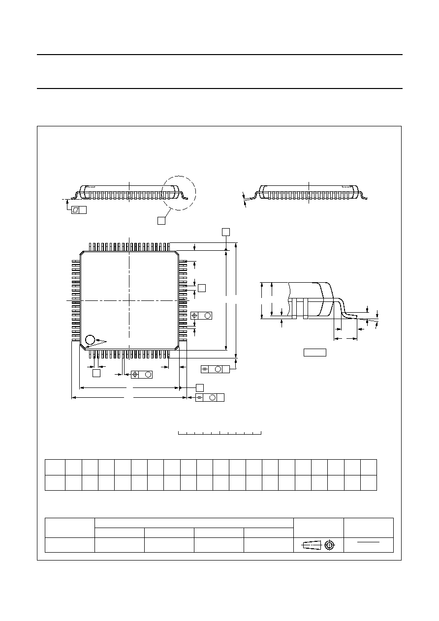
1998 Aug 26
71
Philips Semiconductors
Product specification
Low voltage 8-bit microcontroller with
6-kbyte embedded RAM
SZF2002
28 PACKAGE OUTLINE
UNIT
A
max.
A
1
A
2
A
3
b
p
c
E
(1)
e
H
E
L
L
p
Z
y
w
v
REFERENCES
OUTLINE
VERSION
EUROPEAN
PROJECTION
ISSUE DATE
IEC
JEDEC
EIAJ
mm
1.6
0.16
0.04
1.5
1.3
0.25
0.27
0.13
0.18
0.12
12.1
11.9
0.5
14.15
13.85
1.45
1.05
7
0
o
o
0.15
0.1
0.2
1.0
DIMENSIONS (mm are the original dimensions)
Note
1. Plastic or metal protrusions of 0.25 mm maximum per side are not included.
0.75
0.30
SOT315-1
97-07-15
95-12-19
D
(1)
(1)
(1)
12.1
11.9
H
D
14.15
13.85
E
Z
1.45
1.05
D
b
p
e
E
A
1
A
L
p
detail X
L
(A )
3
B
20
c
D
H
b
p
E
H
A
2
v
M
B
D
Z D
A
Z E
e
v
M
A
X
1
80
61
60
41
40
21
y
pin 1 index
w
M
w
M
0
5
10 mm
scale
LQFP80: plastic low profile quad flat package; 80 leads; body 12 x 12 x 1.4 mm
SOT315-1

1998 Aug 26
72
Philips Semiconductors
Product specification
Low voltage 8-bit microcontroller with
6-kbyte embedded RAM
SZF2002
29 SOLDERING
29.1
Introduction
There is no soldering method that is ideal for all IC
packages. Wave soldering is often preferred when
through-hole and surface mounted components are mixed
on one printed-circuit board. However, wave soldering is
not always suitable for surface mounted ICs, or for
printed-circuits with high population densities. In these
situations reflow soldering is often used.
This text gives a very brief insight to a complex technology.
A more in-depth account of soldering ICs can be found in
our
"Data Handbook IC26; Integrated Circuit Packages"
(order code 9398 652 90011).
29.2
Reflow soldering
Reflow soldering techniques are suitable for all LQFP
packages.
Reflow soldering requires solder paste (a suspension of
fine solder particles, flux and binding agent) to be applied
to the printed-circuit board by screen printing, stencilling or
pressure-syringe dispensing before package placement.
Several methods exist for reflowing; for example,
infrared/convection heating in a conveyor type oven.
Throughput times (preheating, soldering and cooling) vary
between 50 and 300 seconds depending on heating
method. Typical reflow peak temperatures range from
215 to 250
∞
C.
29.3
Wave soldering
Wave soldering is not recommended for LQFP packages.
This is because of the likelihood of solder bridging due to
closely-spaced leads and the possibility of incomplete
solder penetration in multi-lead devices.
CAUTION
Wave soldering is NOT applicable for all LQFP
packages with a pitch (e) equal or less than 0.5 mm.
If wave soldering cannot be avoided, for LQFP
packages with a pitch (e) larger than 0.5 mm, the
following conditions must be observed:
∑
A double-wave (a turbulent wave with high upward
pressure followed by a smooth laminar wave)
soldering technique should be used.
∑
The footprint must be at an angle of 45
∞
to the board
direction and must incorporate solder thieves
downstream and at the side corners.
During placement and before soldering, the package must
be fixed with a droplet of adhesive. The adhesive can be
applied by screen printing, pin transfer or syringe
dispensing. The package can be soldered after the
adhesive is cured.
Maximum permissible solder temperature is 260
∞
C, and
maximum duration of package immersion in solder is
10 seconds, if cooled to less than 150
∞
C within
6 seconds. Typical dwell time is 4 seconds at 250
∞
C.
A mildly-activated flux will eliminate the need for removal
of corrosive residues in most applications.
29.4
Repairing soldered joints
Fix the component by first soldering two diagonally-
opposite end leads. Use only a low voltage soldering iron
(less than 24 V) applied to the flat part of the lead. Contact
time must be limited to 10 seconds at up to 300
∞
C. When
using a dedicated tool, all other leads can be soldered in
one operation within 2 to 5 seconds between
270 and 320
∞
C.
1998 Aug 26
73
Philips Semiconductors
Product specification
Low voltage 8-bit microcontroller with
6-kbyte embedded RAM
SZF2002
30 DEFINITIONS
31 LIFE SUPPORT APPLICATIONS
These products are not designed for use in life support appliances, devices, or systems where malfunction of these
products can reasonably be expected to result in personal injury. Philips customers using or selling these products for
use in such applications do so at their own risk and agree to fully indemnify Philips for any damages resulting from such
improper use or sale.
32 PURCHASE OF PHILIPS I
2
C COMPONENTS
Data sheet status
Objective specification
This data sheet contains target or goal specifications for product development.
Preliminary specification
This data sheet contains preliminary data; supplementary data may be published later.
Product specification
This data sheet contains final product specifications.
Limiting values
Limiting values given are in accordance with the Absolute Maximum Rating System (IEC 134). Stress above one or
more of the limiting values may cause permanent damage to the device. These are stress ratings only and operation
of the device at these or at any other conditions above those given in the Characteristics sections of the specification
is not implied. Exposure to limiting values for extended periods may affect device reliability.
Application information
Where application information is given, it is advisory and does not form part of the specification.
Purchase of Philips I
2
C components conveys a license under the Philips' I
2
C patent to use the
components in the I
2
C system provided the system conforms to the I
2
C specification defined by
Philips. This specification can be ordered using the code 9398 393 40011.

1998 Aug 26
74
Philips Semiconductors
Product specification
Low voltage 8-bit microcontroller with
6-kbyte embedded RAM
SZF2002
NOTES

1998 Aug 26
75
Philips Semiconductors
Product specification
Low voltage 8-bit microcontroller with
6-kbyte embedded RAM
SZF2002
NOTES

Internet: http://www.semiconductors.philips.com
Philips Semiconductors ≠ a worldwide company
© Philips Electronics N.V. 1998
SCA60
All rights are reserved. Reproduction in whole or in part is prohibited without the prior written consent of the copyright owner.
The information presented in this document does not form part of any quotation or contract, is believed to be accurate and reliable and may be changed
without notice. No liability will be accepted by the publisher for any consequence of its use. Publication thereof does not convey nor imply any license
under patent- or other industrial or intellectual property rights.
Middle East: see Italy
Netherlands: Postbus 90050, 5600 PB EINDHOVEN, Bldg. VB,
Tel. +31 40 27 82785, Fax. +31 40 27 88399
New Zealand: 2 Wagener Place, C.P.O. Box 1041, AUCKLAND,
Tel. +64 9 849 4160, Fax. +64 9 849 7811
Norway: Box 1, Manglerud 0612, OSLO,
Tel. +47 22 74 8000, Fax. +47 22 74 8341
Pakistan: see Singapore
Philippines: Philips Semiconductors Philippines Inc.,
106 Valero St. Salcedo Village, P.O. Box 2108 MCC, MAKATI,
Metro MANILA, Tel. +63 2 816 6380, Fax. +63 2 817 3474
Poland: Ul. Lukiska 10, PL 04-123 WARSZAWA,
Tel. +48 22 612 2831, Fax. +48 22 612 2327
Portugal: see Spain
Romania: see Italy
Russia: Philips Russia, Ul. Usatcheva 35A, 119048 MOSCOW,
Tel. +7 095 755 6918, Fax. +7 095 755 6919
Singapore: Lorong 1, Toa Payoh, SINGAPORE 319762,
Tel. +65 350 2538, Fax. +65 251 6500
Slovakia: see Austria
Slovenia: see Italy
South Africa: S.A. PHILIPS Pty Ltd., 195-215 Main Road Martindale,
2092 JOHANNESBURG, P.O. Box 7430 Johannesburg 2000,
Tel. +27 11 470 5911, Fax. +27 11 470 5494
South America: Al. Vicente Pinzon, 173, 6th floor,
04547-130 S√O PAULO, SP, Brazil,
Tel. +55 11 821 2333, Fax. +55 11 821 2382
Spain: Balmes 22, 08007 BARCELONA,
Tel. +34 93 301 6312, Fax. +34 93 301 4107
Sweden: Kottbygatan 7, Akalla, S-16485 STOCKHOLM,
Tel. +46 8 5985 2000, Fax. +46 8 5985 2745
Switzerland: Allmendstrasse 140, CH-8027 ZÐRICH,
Tel. +41 1 488 2741 Fax. +41 1 488 3263
Taiwan: Philips Semiconductors, 6F, No. 96, Chien Kuo N. Rd., Sec. 1,
TAIPEI, Taiwan Tel. +886 2 2134 2865, Fax. +886 2 2134 2874
Thailand: PHILIPS ELECTRONICS (THAILAND) Ltd.,
209/2 Sanpavuth-Bangna Road Prakanong, BANGKOK 10260,
Tel. +66 2 745 4090, Fax. +66 2 398 0793
Turkey: Talatpasa Cad. No. 5, 80640 GÐLTEPE/ISTANBUL,
Tel. +90 212 279 2770, Fax. +90 212 282 6707
Ukraine: PHILIPS UKRAINE, 4 Patrice Lumumba str., Building B, Floor 7,
252042 KIEV, Tel. +380 44 264 2776, Fax. +380 44 268 0461
United Kingdom: Philips Semiconductors Ltd., 276 Bath Road, Hayes,
MIDDLESEX UB3 5BX, Tel. +44 181 730 5000, Fax. +44 181 754 8421
United States: 811 East Arques Avenue, SUNNYVALE, CA 94088-3409,
Tel. +1 800 234 7381
Uruguay: see South America
Vietnam: see Singapore
Yugoslavia: PHILIPS, Trg N. Pasica 5/v, 11000 BEOGRAD,
Tel. +381 11 625 344, Fax.+381 11 635 777
For all other countries apply to: Philips Semiconductors,
International Marketing & Sales Communications, Building BE-p, P.O. Box 218,
5600 MD EINDHOVEN, The Netherlands, Fax. +31 40 27 24825
Argentina: see South America
Australia: 34 Waterloo Road, NORTH RYDE, NSW 2113,
Tel. +61 2 9805 4455, Fax. +61 2 9805 4466
Austria: Computerstr. 6, A-1101 WIEN, P.O. Box 213, Tel. +43 160 1010,
Fax. +43 160 101 1210
Belarus: Hotel Minsk Business Center, Bld. 3, r. 1211, Volodarski Str. 6,
220050 MINSK, Tel. +375 172 200 733, Fax. +375 172 200 773
Belgium: see The Netherlands
Brazil: see South America
Bulgaria: Philips Bulgaria Ltd., Energoproject, 15th floor,
51 James Bourchier Blvd., 1407 SOFIA,
Tel. +359 2 689 211, Fax. +359 2 689 102
Canada: PHILIPS SEMICONDUCTORS/COMPONENTS,
Tel. +1 800 234 7381
China/Hong Kong: 501 Hong Kong Industrial Technology Centre,
72 Tat Chee Avenue, Kowloon Tong, HONG KONG,
Tel. +852 2319 7888, Fax. +852 2319 7700
Colombia: see South America
Czech Republic: see Austria
Denmark: Prags Boulevard 80, PB 1919, DK-2300 COPENHAGEN S,
Tel. +45 32 88 2636, Fax. +45 31 57 0044
Finland: Sinikalliontie 3, FIN-02630 ESPOO,
Tel. +358 9 615800, Fax. +358 9 61580920
France: 51 Rue Carnot, BP317, 92156 SURESNES Cedex,
Tel. +33 1 40 99 6161, Fax. +33 1 40 99 6427
Germany: Hammerbrookstraþe 69, D-20097 HAMBURG,
Tel. +49 40 23 53 60, Fax. +49 40 23 536 300
Greece: No. 15, 25th March Street, GR 17778 TAVROS/ATHENS,
Tel. +30 1 4894 339/239, Fax. +30 1 4814 240
Hungary: see Austria
India: Philips INDIA Ltd, Band Box Building, 2nd floor,
254-D, Dr. Annie Besant Road, Worli, MUMBAI 400 025,
Tel. +91 22 493 8541, Fax. +91 22 493 0966
Indonesia: PT Philips Development Corporation, Semiconductors Division,
Gedung Philips, Jl. Buncit Raya Kav.99-100, JAKARTA 12510,
Tel. +62 21 794 0040 ext. 2501, Fax. +62 21 794 0080
Ireland: Newstead, Clonskeagh, DUBLIN 14,
Tel. +353 1 7640 000, Fax. +353 1 7640 200
Israel: RAPAC Electronics, 7 Kehilat Saloniki St, PO Box 18053,
TEL AVIV 61180, Tel. +972 3 645 0444, Fax. +972 3 649 1007
Italy: PHILIPS SEMICONDUCTORS, Piazza IV Novembre 3,
20124 MILANO, Tel. +39 2 6752 2531, Fax. +39 2 6752 2557
Japan: Philips Bldg 13-37, Kohnan 2-chome, Minato-ku,
TOKYO 108-8507, Tel. +81 3 3740 5130, Fax. +81 3 3740 5077
Korea: Philips House, 260-199 Itaewon-dong, Yongsan-ku, SEOUL,
Tel. +82 2 709 1412, Fax. +82 2 709 1415
Malaysia: No. 76 Jalan Universiti, 46200 PETALING JAYA, SELANGOR,
Tel. +60 3 750 5214, Fax. +60 3 757 4880
Mexico: 5900 Gateway East, Suite 200, EL PASO, TEXAS 79905,
Tel. +9-5 800 234 7381
Printed in The Netherlands
455104/100/01/pp76
Date of release: 1998 Aug 26
Document order number:
9397 750 02944