 | –≠–ª–µ–∫—Ç—Ä–æ–Ω–Ω—ã–π –∫–æ–º–ø–æ–Ω–µ–Ω—Ç: TDA1308T | –°–∫–∞—á–∞—Ç—å:  PDF PDF  ZIP ZIP |

August 1994
2
Philips Semiconductors
Product specification
Class AB stereo headphone driver
TDA1308
FEATURES
∑
Wide temperature range
∑
No switch ON/OFF clicks
∑
Excellent power supply ripple rejection
∑
Low power consumption
∑
Short-circuit resistant
∑
High performance
≠ high signal-to-noise ratio
≠ high slew rate
≠ low distortion
∑
Large output voltage swing.
GENERAL DESCRIPTION
The TDA1308 is an integrated class AB stereo headphone
driver contained in an SO8 or a DIP8 plastic package. The
device is fabricated in a 1 mm CMOS process and has
been primarily developed for portable digital audio
applications.
QUICK REFERENCE DATA
V
DD
= 5 V; V
SS
= 0 V; T
amb
= 25
∞
C; f
i
= 1 kHz; R
L
= 32
; unless otherwise specified.
Note
1. V
DD
= 5 V; V
O(p-p)
= 3.5 V (at 0 dB).
ORDERING INFORMATION
SYMBOL
PARAMETER
CONDITIONS
MIN.
TYP.
MAX.
UNIT
V
DD
supply voltage
single
3.0
5.0
7.0
V
dual
1.5
2.5
3.5
V
V
SS
negative supply voltage
-
1.5
-
2.5
-
3.5
V
I
DD
supply current
no load
-
3
5
mA
P
tot
total power dissipation
no load
-
15
25
mW
P
o
maximum output power
THD < 0.1%; note 1
-
60
-
mW
(THD + N)/S
total harmonic distortion plus
noise-to-signal ratio
note 1
-
0.03
0.06
%
-
-
70
-
65
dB
R
L
= 5 k
-
-
101
-
dB
S/N
signal-to-noise ratio
100
110
-
dB
cs
channel separation
-
70
-
dB
R
L
= 5 k
-
105
-
dB
PSRR
power supply ripple rejection f
i
= 100 Hz; V
ripple(p-p)
= 100 mV
-
90
-
dB
T
amb
operating ambient
temperature
-
40
-
+85
∞
C
TYPE NUMBER
PACKAGE
NAME
DESCRIPTION
VERSION
TDA1308
DIP8
plastic dual in-line package; 8 leads (300 mil)
SOT97-1
TDA1308T
SO8
plastic small outline package; 8 leads; body width 3.9 mm
SOT96-1
August 1994
3
Philips Semiconductors
Product specification
Class AB stereo headphone driver
TDA1308
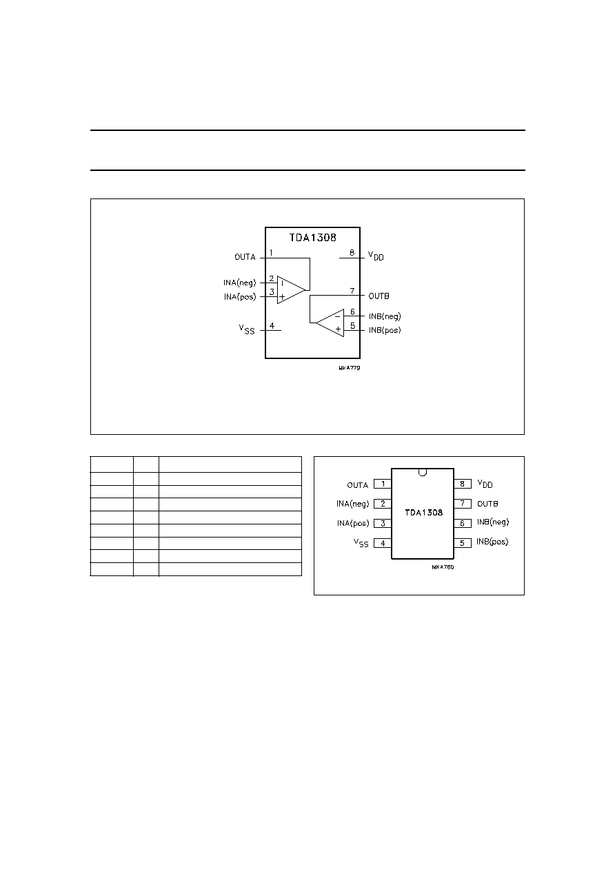
BLOCK DIAGRAM
Fig.1 Block diagram.
PINNING
SYMBOL
PIN
DESCRIPTION
OUTA
1
output A
INA(neg)
2
inverting input A
INA(pos)
3
non-inverting input A
V
SS
4
negative supply
INB(pos)
5
non-inverting input B
INB(neg)
6
inverting input B
OUTB
7
output B
V
DD
8
positive supply
Fig.2 Pin configuration.
August 1994
4
Philips Semiconductors
Product specification
Class AB stereo headphone driver
TDA1308
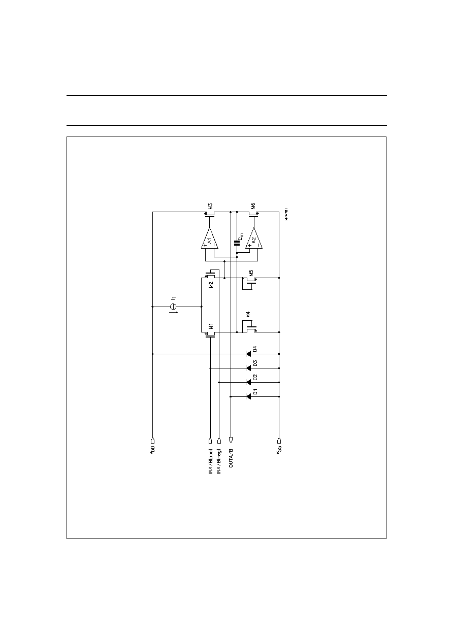
Fig.3 Equivalent schematic diagram.
August 1994
5
Philips Semiconductors
Product specification
Class AB stereo headphone driver
TDA1308
LIMITING VALUES
In accordance with the Absolute Maximum Rating System (IEC134).
Notes
1. Human body model: C = 100 pF; R = 1500
; 3 pulses positive plus 3 pulses negative.
2. Machine model: C = 200 pF: L = 0.5 mH: R = 0
; 3 pulses positive plus 3 pulses negative.
THERMAL CHARACTERISTICS
QUALITY SPECIFICATION
In accordance with
"UZW-BO/FQ-0601". The numbers of the quality specification can be found in the "Quality Reference
Handbook". The handbook can be ordered using the code 9398 510 63011.
SYMBOL
PARAMETER
CONDITIONS
MIN.
MAX.
UNIT
V
DD
supply voltage
0
8.0
V
t
SC(O)
output short-circuit duration
T
amb
= 25
∞
C; P
tot
= 1 W
20
-
s
T
stg
storage temperature
-
65
+150
∞
C
T
amb
operating ambient temperature
-
40
+85
∞
C
V
esd
electrostatic discharge
note 1
-
2000
+2000
V
note 2
-
200
+200
V
SYMBOL
PARAMETER
VALUE
UNIT
R
th j-a
thermal resistance from junction to ambient in free air
DIP8
109
K/W
SO8
210
K/W
August 1994
6
Philips Semiconductors
Product specification
Class AB stereo headphone driver
TDA1308
CHARACTERISTICS
V
DD
= 5 V; V
SS
= 0 V; T
amb
= 25
∞
C; f
i
= 1 kHz; R
L
= 32
; unless otherwise specified.
Notes
1. Values are proportional to V
DD
; (THD + N)/S < 0.1%.
2. V
DD
= 5.0 V; V
O(p-p)
= 3.5 V (at 0 dB).
SYMBOL
PARAMETER
CONDITIONS
MIN.
TYP.
MAX.
UNIT
Supplies
V
DD
supply voltage
single
3.0
5.0
7.0
V
dual
1.5
2.5
3.5
V
V
SS
negative supply voltage
-
1.5
-
2.5
-
3.5
V
I
DD
supply current
no load
-
3
5
mA
P
tot
total power dissipation
no load
-
15
25
mW
DC characteristics
V
I(os)
input offset voltage
-
10
-
mV
I
bias
input bias current
-
10
-
pA
V
CM
common mode voltage
0
-
3.5
V
G
v
open-loop voltage gain
R
L
= 5 k
-
70
-
dB
I
O
maximum output current
(THD + N)/S < 0.1%
-
60
-
mA
R
O
output resistance
-
0.25
-
V
O
output voltage swing
note 1
0.75
-
4.25
V
R
L
= 16
;
note 1
1.5
-
3.5
V
R
L
= 5 k
;
note 1
0.1
-
4.9
V
PSRR
power supply rejection ratio
f
i
= 100 Hz;
V
ripple(p-p)
= 100 mV
-
90
-
dB
cs
channel separation
-
70
-
dB
R
L
= 5 k
-
105
-
dB
C
L
load capacitance
-
-
200
pF
AC characteristics
(THD + N)/S total harmonic distortion plus
noise-to-signal ratio
note 2
-
-
70
-
65
dB
-
0.03
0.06
%
note 2; R
L
= 5 k
-
-
101
-
dB
-
0.0009
-
%
S/N
signal-to-noise ratio
100
110
-
dB
f
G
unity gain frequency
open-loop; R
L
= 5 k
-
5.5
-
MHz
P
o
maximum output power
(THD + N)/S < 0.1%
-
60
-
mW
C
i
input capacitance
-
3
-
pF
SR
slew rate
unity gain inverting
-
5
-
V/
µ
s
B
power bandwidth
unity gain inverting
-
20
-
kHz