 | –≠–ª–µ–∫—Ç—Ä–æ–Ω–Ω—ã–π –∫–æ–º–ø–æ–Ω–µ–Ω—Ç: TDA1543 | –°–∫–∞—á–∞—Ç—å:  PDF PDF  ZIP ZIP |
DATA SHEET
Product specification
File under Integrated Circuits, IC01
February 1991
INTEGRATED CIRCUITS
TDA1543
Dual 16-bit DAC (economy version)
(I
2
S input format)

February 1991
2
Philips Semiconductors
Product specification
Dual 16-bit DAC (economy version)
(I
2
S input format)
TDA1543
FEATURES
∑
Low distortion
∑
16-bit dynamic range
∑
4
◊
oversampling possible
∑
Single 5 V power supply
∑
No external components required
∑
No requirement for external deglitcher circuitry due to
fast settling output current
∑
Adjustable bias current
∑
Internal timing and control circuits
∑
I
2
S input format: time multiplexed, two's complement,
TTL.
GENERAL DESCRIPTION
The TDA1543 is a monolithic integrated dual 16-bit
digital-to-analog converter (DAC) designed as an
economy version for use in hi-fi digital audio equipment
such as Compact Disc players, digital tape or cassette
recorders, digital sound in TV sets and in digital amplifiers.
ORDERING INFORMATION
Notes
1. SOT97-1; 1996 August 13.
2. SOT162-1 1996 August 13.
QUICK REFERENCE DATA
EXTENDED
TYPE NUMBER
PACKAGE
PINS
PIN POSITION
MATERIAL
CODE
TDA1543
(1)
8
DIL
plastic
SOT97
TDA1543T
(2)
16
mini-pack
plastic
SO16L;SOT162A
SYMBOL
PARAMETER
CONDITIONS
MIN.
TYP.
MAX.
UNIT
V
DD
supply voltage
3.0
5.0
8.0
V
I
DD
supply current
-
50
60
mA
I
FS
full scale output current
1.95
2.30
2.65
mA
THD
total harmonic distortion
including noise
-
-
75
-
70
dB
at 0 dB
-
0.018
0.032
%
THD
total harmonic distortion
including noise
-
-
30
-
23
dB
at
-
60 dB
-
3.2
7.9
%
t
cs
current settling time to
±
1 LSB
-
0.5
-
µ
s
BR
input bit rate at data input
-
-
9.2
Mbits/s
f
BCK
clock frequency at clock input
-
-
9.2
MHz
S/N
signal-to-noise ratio
at bipolar zero
90
96
-
dB
TC
FS
full scale temperature coefficient
at analog outputs
(AOL; AOR)
-
±
500
◊
10
-
6
-
K
-
1
T
amb
operating ambient temperature
range
-
30
-
+
85
∞
C
P
tot
total power dissipation
-
250
-
mW
I
bias
bias current (adjustable)
-
0.6
-
5.0
mA

February 1991
3
Philips Semiconductors
Product specification
Dual 16-bit DAC (economy version)
(I
2
S input format)
TDA1543
handbook, full pagewidth
MEA110
5-BIT
P
ASSIVE
DIVIDER
CONTR
OL
&
TIMING
LEFT OUTPUT LA
TCH
LEFT BIT SWITCHES
RIGHT OUTPUT LA
TCH
RIGHT BIT SWITCHES
RIGHT INPUT LA
TCH
11-BIT
P
ASSIVE
DIVIDER
11-BIT
P
ASSIVE
DIVIDER
5-BIT
P
ASSIVE
DIVIDER
CURRENT
SOURCE
ADDRESS POINTER
REFERENCE
SOURCE
CURRENT
SOURCE
LEFT INPUT LA
TCH
AO
L
AO
R
3.3 nF
1.2 k
(2)
V
out
left
V
ref
r
ight
V
out
3.3 nF
1.2 k
(2)
V
ref
AO
L
I
AO
R
I
BRI
BLI
BRI
BLI
V
ref
I
ref
R
bias
5 V
100
nF
g
round
V
DD
4
5
7
8
6
TD
A1543
LE
LE
LE
1
2
3
BCK
WS
D
ATA
(1)
(1)
Optional.
(2)
2
◊
1/2 NE5532.
Fig.1 Block diagram.
February 1991
4
Philips Semiconductors
Product specification
Dual 16-bit DAC (economy version)
(I
2
S input format)
TDA1543
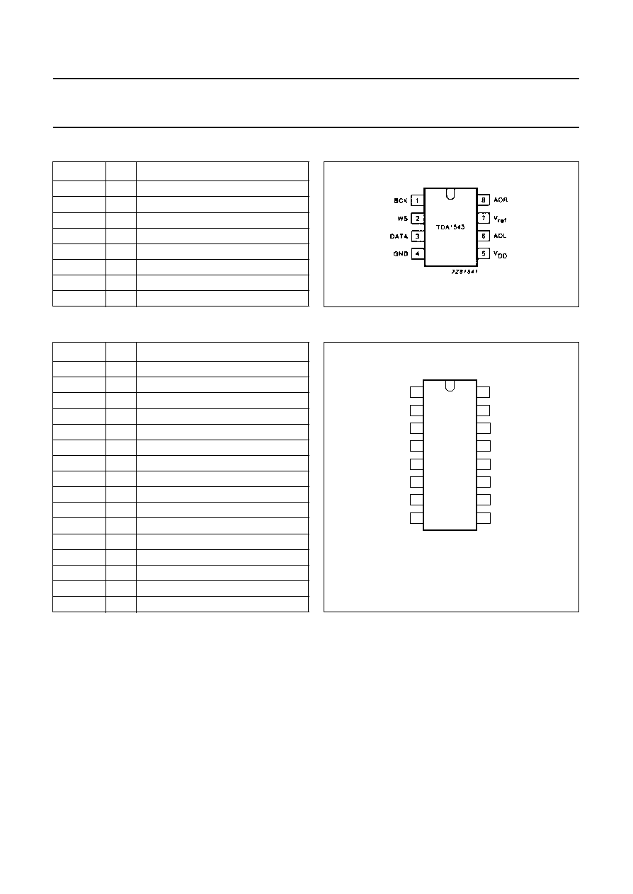
PINNING
SYMBOL
PIN
DESCRIPTION
BCK
1
bit clock input
WS
2
word select input
DATA
3
data input
GND
4
ground
V
DD
5
+
5 V supply voltage
AOL
6
left channel voltage output
V
ref
7
reference voltage output
AOR
8
right channel output
Fig.2 Pin configuration TDA1543.
PINNING
SYMBOL
PIN
DESCRIPTION
n.c.
1
not connected
n.c.
2
not connected
BCK
3
bit clock input
WS
4
word select input
DATA
5
data input
GND
6
ground
n.c.
7
not connected
n.c.
8
not connected
n.c.
9
not connected
n.c.
10
not connected
V
DD
11
+
5 V supply voltage
AOL
12
left channel output
V
ref
13
reference voltage output
AOR
14
right channel output
n.c.
15
not connected
n.c.
16
not connected
Fig.3 Pin configuration TDA1543T.
handbook, halfpage
MEA107
1
2
3
4
5
6
7
8
16
15
14
13
12
11
10
9
VDD
GND
n.c.
DATA
Vref
BCK
AOR
AOL
WS
n.c.
n.c.
TDA1543T
n.c.
n.c.
n.c.
n.c.
n.c.

February 1991
5
Philips Semiconductors
Product specification
Dual 16-bit DAC (economy version)
(I
2
S input format)
TDA1543
AOL
AOR
TDA1543
I bias
I DAC
VDD
TDA1543
BCK
WS
DATA
TDA1543
Vref
VDD
VDD
VDD
MEA109
Fig.4 Circuits at the input and output pins.
(b) output pin V
ref
.
(c) output pins AOL and AOR.
(a) input pins BCK, WS and DATA.

February 1991
6
Philips Semiconductors
Product specification
Dual 16-bit DAC (economy version)
(I
2
S input format)
TDA1543
FUNCTIONAL DESCRIPTION
The TDA1543 accepts input serial data formats in two's complement with any bit length. Left and right data words are
time multiplexed. The most significant bit (bit 1) must always be first. The format of data input is shown in Fig.5 and Fig.6.
This flexible input data format (I
2
S) allows easy interfacing with signal processing chips such as interpolation filters, error
correction circuits and audio signal processor circuits (ASP).
The high maximum input bit-rate and fast settling current facilitates application in 4
◊
oversampling systems. An
adjustable current is added to the output currents to bias output operational amplifiers (OP1; OP2) for maximum dynamic
range (see Fig.1).
With a LOW level on the word select (WS) input data is placed in the left input register and with a HIGH level on the WS
input data is placed in the right input register. The data in the input registers is simultaneously latched in the output
registers which control the bit switches.
The output current of the DAC is a sink current. The current I
ref
at the V
ref
output is adjusted by a resistor or a current
source. The current I
ref
is amplified with gain A
Ibias
to the bias currents (I
BL
; I
BR
) which are added to the output currents.
LIMITING VALUES
In accordance with the Absolute Maximum System (lEC 134)
THERMAL RESISTANCE
* Equivalent to discharging a 100 pF capacitor through a 1.5 k
series resistor.
SYMBOL
PARAMETER
CONDITIONS
MIN.
MAX.
UNIT
V
DD
supply voltage range
0
9
V
T
XTAL
crystal temperature
-
+150
∞
C
T
stg
storage temperature range
-
55
+150
∞
C
T
amb
operating ambient temperature
range
-
30
+85
∞
C
V
es
electrostatic handling*
-
2000
+2000
V
SYMBOL
PARAMETER
TYP.
UNIT
R
th j-a
from junction to ambient
100
K/W

February 1991
7
Philips Semiconductors
Product specification
Dual 16-bit DAC (economy version)
(I
2
S input format)
TDA1543
CHARACTERISTICS
V
DD
= 5 V; T
amb
=
+
25
∞
C; I
ref
= 0 mA; measured in the circuit of Fig.1; unless otherwise specified
SYMBOL
PARAMETER
CONDITIONS
MIN.
TYP.
MAX.
UNIT
Supply
V
DD
supply voltage range
3.0
5.0
8.0
V
I
DD
supply current
note 1
-
50
60
mA
RR
ripple rejection
note 2
-
50
-
dB
Digital inputs
input current pins (1, 2 and 3)
I
IL
digital inputs LOW
V
l
= 0.8 V
-
-
-
0.4
mA
I
IH
digital inputs HIGH
V
l
= 2.0 V
-
-
20
µ
A
input frequency/bit rate
f
BCK
clock input pin 1
-
-
9.2
MHz
BR
bit rate data input pin 3
-
-
9.2
Mbits/s
f
WS
word select input pin 2
-
-
192
kHz
Analog outputs (AOL; AOR)
Res
resolution
-
-
16
bits
output voltage compliance
V
OC(AC)
AC
-
±
25
-
mV
V
OC(DC)
DC
1.8
-
V
DD
-
1.2
V
I
FS
full scale current
1.95
2.30
2.65
mA
T
CFS
full scale temperature coefficient
-
±
500
◊
10
-
6
-
K
-
1
I
offset
offset current
I
ref
= 0 mA
-
0.1
0.0
0.1
mA
I
bias
bias current (adjustable)
-
0.6
-
5.0
mA
AI
bias
bias current gain
1.9
2.0
2.1
Analog outputs (V
ref
)
V
ref
reference voltage output
2.10
2.20
2.30
V
I
ref
reference current output
-
0.3
-
2.5
mA
THD
total harmonic distortion
including noise at
-
75
-
70
dB
0 dB;
note 3, Fig.7
0.018
0.032
%
THD
total harmonic distortion
including noise at
-
-
30
-
23
dB
-
60 dB;
note 3, Fig.7
-
3.2
7.9
%
t
cs
settling time
±
1 LSB
-
0.5
-
µ
s
channel separation
85
90
-
dB
|d
IO
|
unbalance between outputs
note 4
-
<
0.2
0.3
dB
|t
d
|
time delay between outputs
-
<
0.2
-
µ
s
S/N
signal-to-noise ratio
at bipolar zero;
note 5
90
96
-
dB

February 1991
8
Philips Semiconductors
Product specification
Dual 16-bit DAC (economy version)
(I
2
S input format)
TDA1543
Notes to the characteristics
1. Measured at I
AOL
= 0 mA and I
AOR
= 0 mA (code 8000H) and I
bias
= 0 mA.
2. V
ripple
= 1% of supply voltage and f
ripple
= 100 Hz.
3. Measured with 1 kHz sinewave generated at a sampling rate of 192 kHz.
4. Measured with 1 kHz full scale sinewave generated at a sampling rate of 192 kHz.
5. At code 0000H.
6. At this point t
HD;DAT
= 0 ns, this value has been fixed on 2 ns due to tolerances.
Timing (Fig.5)
t
r
rise time
-
-
32
ns
t
f
fall time
-
-
32
ns
t
CY
bit clock cycle time
108
-
-
ns
t
HB
bit clock HIGH time
22
-
-
ns
t
LB
bit clock LOW time
22
-
-
ns
t
SU;DAT
data set-up time
32
-
-
ns
t
HD;DAT
data hold time to bit clock
note 6
2
-
-
ns
t
HD;WS
word select hold time
note 6
2
-
-
ns
t
SU;WS
word select set-up time
32
-
-
ns
SYMBOL
PARAMETER
CONDITIONS
MIN.
TYP.
MAX.
UNIT
Fig.5 Format of input signals (I
2
S format).

February 1991
9
Philips Semiconductors
Product specification
Dual 16-bit DAC (economy version)
(I
2
S input format)
TDA1543
pagewidth
DATA
BCK
WS
LEFT
RIGHT
LSB
MSB
LSB
MSB
MEA112
Fig.6 Format of input signals.
handbook, full pagewidth
0.01
1
0.1
10
MEA111-1
THD
(%)
frequency (Hz)
10
10
3
≠ 90
≠ 70
≠ 20
THD
(dB)
10
2
10
4
≠ 50
≠ 80
≠ 40
≠ 60
≠ 30
(1)
(2)
(3)
Fig.7 Distortion as a function of frequency (4FS).
(1) Measured including all distortion plus noise over a 20 kHz bandwidth at a level of
-
60 dB.
(2) Measured including all distortion plus noise over a 20 kHz bandwidth at a level of
-
24 dB.
(3) Measured including all distortion plus noise over a 20 kHz bandwidth at a level of
-
0 dB.

February 1991
10
Philips Semiconductors
Product specification
Dual 16-bit DAC (economy version)
(I
2
S input format)
TDA1543
Notes to Fig.7
∑
The sample frequency 4FS: 176.4 kHz.
∑
The supply voltage at the measurement = + 5 V (DC).
∑
Ref: 0 dB is the output level of a full scale digital sine wave stimulus.
∑
The graphs are constructed from average values of a small amount of engineering samples therefore no guarantee
for typical values is implied.
∑
The arrows indicate the specification limits for 0 dB and
-
60 dB level signals.

February 1991
11
Philips Semiconductors
Product specification
Dual 16-bit DAC (economy version)
(I
2
S input format)
TDA1543
PACKAGE OUTLINES
REFERENCES
OUTLINE
VERSION
EUROPEAN
PROJECTION
ISSUE DATE
IEC
JEDEC
EIAJ
SOT97-1
92-11-17
95-02-04
UNIT
A
max.
1
2
b
1
(1)
(1)
(1)
b
2
c
D
E
e
M
Z
H
L
mm
DIMENSIONS (inch dimensions are derived from the original mm dimensions)
A
min.
A
max.
b
max.
w
M
E
e
1
1.73
1.14
0.53
0.38
0.36
0.23
9.8
9.2
6.48
6.20
3.60
3.05
0.254
2.54
7.62
8.25
7.80
10.0
8.3
1.15
4.2
0.51
3.2
inches
0.068
0.045
0.021
0.015
0.014
0.009
1.07
0.89
0.042
0.035
0.39
0.36
0.26
0.24
0.14
0.12
0.01
0.10
0.30
0.32
0.31
0.39
0.33
0.045
0.17
0.020
0.13
b
2
050G01
MO-001AN
M
H
c
(e )
1
M
E
A
L
seating plane
A
1
w
M
b
1
e
D
A
2
Z
8
1
5
4
b
E
0
5
10 mm
scale
Note
1. Plastic or metal protrusions of 0.25 mm maximum per side are not included.
pin 1 index
DIP8: plastic dual in-line package; 8 leads (300 mil)
SOT97-1

February 1991
12
Philips Semiconductors
Product specification
Dual 16-bit DAC (economy version)
(I
2
S input format)
TDA1543
UNIT
A
max.
A
1
A
2
A
3
b
p
c
D
(1)
E
(1)
(1)
e
H
E
L
L
p
Q
Z
y
w
v
REFERENCES
OUTLINE
VERSION
EUROPEAN
PROJECTION
ISSUE DATE
IEC
JEDEC
EIAJ
mm
inches
2.65
0.30
0.10
2.45
2.25
0.49
0.36
0.32
0.23
10.5
10.1
7.6
7.4
1.27
10.65
10.00
1.1
1.0
0.9
0.4
8
0
o
o
0.25
0.1
DIMENSIONS (inch dimensions are derived from the original mm dimensions)
Note
1. Plastic or metal protrusions of 0.15 mm maximum per side are not included.
1.1
0.4
SOT162-1
8
16
w
M
b
p
D
detail X
Z
e
9
1
y
0.25
075E03
MS-013AA
pin 1 index
0.10
0.012
0.004
0.096
0.089
0.019
0.014
0.013
0.009
0.41
0.40
0.30
0.29
0.050
1.4
0.055
0.42
0.39
0.043
0.039
0.035
0.016
0.01
0.25
0.01
0.004
0.043
0.016
0.01
X
A
A
1
A
2
H
E
L
p
Q
E
c
L
v
M
A
(A )
3
A
0
5
10 mm
scale
92-11-17
95-01-24
SO16: plastic small outline package; 16 leads; body width 7.5 mm
SOT162-1

February 1991
13
Philips Semiconductors
Product specification
Dual 16-bit DAC (economy version)
(I
2
S input format)
TDA1543
SOLDERING
Introduction
There is no soldering method that is ideal for all IC
packages. Wave soldering is often preferred when
through-hole and surface mounted components are mixed
on one printed-circuit board. However, wave soldering is
not always suitable for surface mounted ICs, or for
printed-circuits with high population densities. In these
situations reflow soldering is often used.
This text gives a very brief insight to a complex technology.
A more in-depth account of soldering ICs can be found in
our
"IC Package Databook" (order code 9398 652 90011).
Soldering by dipping or by wave
The maximum permissible temperature of the solder is
260
∞
C; solder at this temperature must not be in contact
with the joint for more than 5 seconds. The total contact
time of successive solder waves must not exceed
5 seconds.
The device may be mounted up to the seating plane, but
the temperature of the plastic body must not exceed the
specified maximum storage temperature (T
stg max
). If the
printed-circuit board has been pre-heated, forced cooling
may be necessary immediately after soldering to keep the
temperature within the permissible limit.
Repairing soldered joints
Apply a low voltage soldering iron (less than 24 V) to the
lead(s) of the package, below the seating plane or not
more than 2 mm above it. If the temperature of the
soldering iron bit is less than 300
∞
C it may remain in
contact for up to 10 seconds. If the bit temperature is
between 300 and 400
∞
C, contact may be up to 5 seconds.
DEFINITIONS
LIFE SUPPORT APPLICATIONS
These products are not designed for use in life support appliances, devices, or systems where malfunction of these
products can reasonably be expected to result in personal injury. Philips customers using or selling these products for
use in such applications do so at their own risk and agree to fully indemnify Philips for any damages resulting from such
improper use or sale.
Data sheet status
Objective specification
This data sheet contains target or goal specifications for product development.
Preliminary specification
This data sheet contains preliminary data; supplementary data may be published later.
Product specification
This data sheet contains final product specifications.
Limiting values
Limiting values given are in accordance with the Absolute Maximum Rating System (IEC 134). Stress above one or
more of the limiting values may cause permanent damage to the device. These are stress ratings only and operation
of the device at these or at any other conditions above those given in the Characteristics sections of the specification
is not implied. Exposure to limiting values for extended periods may affect device reliability.
Application information
Where application information is given, it is advisory and does not form part of the specification.