Document Outline
- FEATURES
- GENERAL DESCRIPTION
- QUICK REFERENCE DATA
- ORDERING INFORMATION
- BLOCK DIAGRAM
- PINNING
- FUNCTIONAL DESCRIPTION
- LIMITING VALUES
- THERMAL CHARACTERISTICS
- DC CHARACTERISTICS
- AC CHARACTERISTICS
- APPLICATION INFORMATION
- PACKAGE OUTLINE
- SOLDERING
- DEFINITIONS
- LIFE SUPPORT APPLICATIONS

DATA SHEET
Product specification
Supersedes data of 1995 Jul 07
File under Integrated Circuits, IC01
1996 May 14
INTEGRATED CIRCUITS
TDA1560Q
40 W car radio high power amplifier

1996 May 14
2
Philips Semiconductors
Product specification
40 W car radio high power amplifier
TDA1560Q
FEATURES
∑
Very high output power
∑
Low power dissipation when used for music signals
∑
Switches to low output power in the event of excessive
heatsink temperatures
∑
Requires few external components
∑
Fixed gain
∑
Low cross-over distortion
∑
No switch-on/switch-off plops
∑
Mode select switch
∑
Low offset voltage at the output
∑
Load dump protection
∑
Short-circuit safe to ground, V
P
and across load
∑
Protected against electrostatic discharge
∑
Thermally protected
∑
Diagnostic facility
∑
Flexible leads.
GENERAL DESCRIPTION
The TDA1560Q is an integrated Bridge-Tied Load (BTL)
class-H high power amplifier. In a load of 8
, the output
power is 40 W typical at a THD of 10%.
The encapsulation is a 17-lead DIL-bent-SIL plastic power
package. The device is primarily developed for car radio
applications.
QUICK REFERENCE DATA
ORDERING INFORMATION
SYMBOL
PARAMETER
CONDITIONS
MIN.
TYP.
MAX.
UNIT
V
P
supply voltage
operating
8.0
14.4
18
V
non-operating
-
-
30
V
load dump protected
-
-
45
V
I
ORM
repetitive peak output current
-
-
4
A
I
q(tot)
total quiescent current
-
100
160
mA
I
sb
standby current
-
5
50
µ
A
G
v
voltage gain
29
30
31
dB
P
o
output power
R
L
= 8
; THD = 10%
-
40
-
W
R
L
= 8
; THD = 0.5%
-
30
-
W
SVRR
supply voltage ripple rejection
f
i
= 100 Hz to 10 kHz;
R
S
= 0
48
55
-
dB
V
no
noise output voltage
-
100
300
µ
V
Z
i
input impedance
180
300
-
k
V
O
DC output offset voltage
-
-
150
mV
TYPE NUMBER
PACKAGE
NAME
DESCRIPTION
VERSION
TDA1560Q
DBS17P
plastic DIL-bent-SIL power package; 17 leads (lead length 12 mm)
SOT243-1

1996 May 14
3
Philips Semiconductors
Product specification
40 W car radio high power amplifier
TDA1560Q
BLOCK DIAGRAM
Fig.1 Block diagram.
handbook, full pagewidth
SUPPLY
SUPPLY
TEMPERATURE
SENSOR
INPUT AND
FEEDBACK
CIRCUIT
13
10
C1
C1n
INPp
INPn
Vref
CDEC
C1p
VP
9
MCD334 - 1
voltage
reference
POWER
STAGE
POWER
STAGE
5
8
C2
7
11
15
16
150
k
150
k
1
2
4
15 k
10 k
17
S1
MODE
GND
GND
GND
disable
disable
VP
VP
12
6
TDA1560Q
LOAD DUMP
TEMPERATURE
AND CURRENT
PROTECTION
3
14
C2n
C2p
OUT2p
OUT1n
VDIAG

1996 May 14
4
Philips Semiconductors
Product specification
40 W car radio high power amplifier
TDA1560Q
PINNING
SYMBOL
PIN
DESCRIPTION
INP
p
1
positive input
INP
n
2
negative input
GND
3
ground
V
ref
4
reference voltage
C2
n
5
capacitor C2 negative terminal
GND
6
ground
OUT1
n
7
output 1 (negative)
C2
p
8
capacitor C2 positive terminal
V
P
9
supply voltage
C1
p
10
capacitor C1 positive terminal
OUT2
p
11
output 2 (positive)
GND
12
ground
C1
n
13
capacitor C1 negative terminal
V
DIAG
14
diagnostic voltage output
C
DEC
15
decoupling
MODE
16
mode select switch input
S1
17
class-B/class-H input switch
Fig.2 Pin configuration.
handbook, halfpage
1
2
3
4
5
6
7
8
9
10
11
12
13
14
15
16
MCD329 - 1
17
GND
OUT1n
C2p
C1p
GND
MODE
OUT2p
DEC
C
INPn
GND
INPp
Vref
C2n
VP
C1n
S1
TDA1560Q
DIAG
V

1996 May 14
5
Philips Semiconductors
Product specification
40 W car radio high power amplifier
TDA1560Q
FUNCTIONAL DESCRIPTION
The TDA1560Q contains a mono class-H BTL output
power amplifier. At low output power, up to 10 W, the
device operates as a normal BTL amplifier. When a larger
output voltage swing is required, the internal supply
voltage is lifted to approximately twice the external supply
voltage. This extra supply voltage is obtained from the
charge in the external electrolytic capacitors. Due to this
momentarily higher supply voltage, the maximum output
power is 40 W typical at a THD of 10%.
In normal use, when the output is driven with music-type
signals, the high output power is only required for a small
percentage of the time. Assuming a music signal has a
normal (Gaussian) amplitude distribution, the reduction in
dissipation is approximately 50% when compared to a
class-B output amplifier with the same output power.
The heatsink should be designed for use with music
signals.
If the device is continuous sine wave driven, instead of
driven with music signals and at a high output power
(class-H operation), the case temperature can rise above
120
∞
C with such a practical heatsink. In this event, the
thermal protection disables the high power supply voltage
and limits the output power to 10 W and the maximum
dissipation to 5 W.
The gain of each amplifier is internally fixed at 30 dB. With
the mode select input the device can be switched to the
following modes:
∑
Low standby current (<50
µ
A)
∑
Mute condition, DC adjusted
∑
On, operation in class-B, limited output power
∑
On, operation in class-H, high output power.
The device can be used as a normal BTL class-AB
amplifier if the electrolytic capacitors C1 and C2 are
omitted; see Fig.6. If the case temperature exceeds
120
∞
C, the device will switch back from class-H to class-B
operation. The high power supply voltage is then disabled
and the output power is limited to 10 W. By measuring the
voltage on the class-B/class-H pin, the actual crystal
temperature can be detected.
The open voltage on the class-B/class-H pin is related to
the global temperature of the crystal. By measuring this
voltage, external actions can be taken to reduce an
excessive temperature (e.g. by cutting off low frequencies
or externally switching to class-B). For the relationship
between the crystal temperature and the voltage on this
pin, see Fig.3.
By forcing a high voltage level on the class-B/class-H pin,
thereby simulating a high temperature, the device can be
externally switched to class-B operation. Similarly, by
forcing a low voltage level on the class-B/class-H pin,
thereby simulating a low temperature, the device can be
forced into class-H operation, even if the case temperature
exceeds 120
∞
C.
The device is fully protected against short-circuiting of the
outputs to ground or V
P
and across the load, high crystal
temperature and electrostatic discharge at all input and
output pins. In the event of a continuing short-circuit to
ground or V
P
, excessive dissipation is prevented because
the output stages will be switched off. The output stages
will be switched on again within 20 ms after the
short-circuit has been removed.
A diagnostic facility is available at pin 14. In normal
conditions the voltage at this pin will be the supply voltage
(V
P
). In the event of the following conditions:
∑
Junction temperature exceeds 150
∞
C
∑
Short-circuit of one of the outputs to ground or to V
P
∑
Load dump; V
P
> 20 V.
The voltage level at pin 14 will be at a constant level of
approximately
1
/
2
V
P
during fault condition. At a short-circuit
over the load, pin 14 will be at
1
/
2
V
P
for approximately
20 ms and V
P
for approximately 50
µ
s.

1996 May 14
6
Philips Semiconductors
Product specification
40 W car radio high power amplifier
TDA1560Q
LIMITING VALUES
In accordance with the Absolute Maximum Rating System (IEC 134).
THERMAL CHARACTERISTICS
SYMBOL
PARAMETER
CONDITIONS
MIN.
MAX.
UNIT
V
P
supply voltage
operating
-
18
V
non-operating
-
30
V
load dump protection; t
r
2.5 ms
-
45
V
I
OSM
non-repetitive peak output current
-
6
A
I
ORM
repetitive peak output current
-
4
A
V
P(sc)
AC and DC short-circuit safe voltage
-
18
V
E
cap
energy handling capability at outputs V
P
= 0
-
200
mJ
I
17
current at pin 17
V
17
< V
P
-
1
-
5
mA
P
tot
total power dissipation
-
60
W
T
stg
storage temperature
-
55
+150
∞
C
T
amb
operating ambient temperature
-
40
-
∞
C
SYMBOL
PARAMETER
VALUE
UNIT
R
th j-a
thermal resistance from junction to ambient in free air
40
K/W
R
th j-case
thermal resistance from junction to case (measured in Fig.6)
3
K/W
Heatsink design
There are two parameters that determine the size of the
heatsink. The first is the rating for the case temperature
and the second is the ambient temperature at which the
amplifier must still deliver its full power in the class-H
mode.
E
XAMPLE
1
With an 8
load and driven with a music signal, the
maximum power dissipation is approximately 6.5 W. If the
amplifier is to deliver its full power at ambient temperatures
up to 50
∞
C the case temperature should not be higher
than120
∞
C for class-H operation.
R
th case-h
= 1 K/W, thus the external heatsink should be:
In this example and with an 8
load, the size of the
heatsink is determined by the rating for the maximum full
power ambient temperature. If the case temperature of the
device exceeds 120
∞
C then the device switches back to
class-B, see "Example 2".
120
50
≠
6.5
----------------------
1.0
≠
10 K/W
=
E
XAMPLE
2
With disabled class-H mode, an 8
load and driven with
a sine wave signal the maximum power dissipation is
approximately 5 W. At a virtual junction temperature of
150
∞
C and T
amb(max)
at 60
∞
C, R
th vj-case
= 3 K/W and
R
th case-h
= 1 K/W the thermal resistance of the heatsink
should be:
In this example the size of the heatsink is determined by
the virtual junction temperature.
150
60
≠
5
----------------------
3
1
14 K/W
=
≠
≠

1996 May 14
7
Philips Semiconductors
Product specification
40 W car radio high power amplifier
TDA1560Q
DC CHARACTERISTICS
V
P
= 14.4 V; R
L
= 8
; T
amb
= 25
∞
C and using 4 K/W heatsink; measured in Fig.6; unless otherwise specified.
Notes
1. The circuit is DC adjusted at V
P
= 8 to 18 V and AC operating at V
P
= 8.5 to 18 V.
2. The DC output voltage, or the common mode voltage on the loudspeaker terminals with respect to ground, is 6.3 V
at output power up to 8.5 W. At higher output power, the common mode voltage will be higher.
3. The voltage at pin 14 is approximately
1
/
2
V
P
in the event of a short-circuit, load dump or temperature protection. Any
circuit connected to pin 14 should have an input resistance of >2 M
and an input capacitance of <5 nF.
4. The DC output offset voltage step is the difference in output offset voltage in the mute condition and the on condition.
The absolute value of this voltage step is given as
+
V
o mute
-
V
o on
< 150 mV.
5. Figure 3 shows the relationship between the global crystal temperature and the open voltage at the
class-B/class-H pin.
6. The maximum voltage on pin 17 is V
P
-
1 (V
P
18 V).
SYMBOL
PARAMETER
CONDITIONS
MIN.
TYP.
MAX.
UNIT
Supply
V
P
supply voltage
note 1
8.0
14.4
18.0
V
I
q(tot)
total quiescent current
-
100
160
mA
V
O
DC output voltage
note 2
-
6.5
-
V
V
O
DC output offset voltage
-
-
150
mV
V
14
diagnostic output voltage
note 3
6
-
8
V
Mode select switch (see Fig.4)
V
16
switch input voltage level
standby condition
0
-
1.2
V
mute condition
2.6
-
3.5
V
class-B operation
4.5
-
7.0
V
class-H operation
8.5
-
V
P
V
I
SW max
maximum switch current
-
-
20
µ
A
I
sb
DC supply current
standby condition
-
5
50
µ
A
V
O
DC output offset voltage
mute condition
-
-
150
mV
mute-on step; note 4
-
-
150
mV
V
O
output signal voltage in mute condition
V
i(max)
= 1 V;
f
i
= 20 Hz to 15 kHz
-
-
2
mV
Class-B/class-H operation (see Fig.3 and note 5)
V
17
switch input voltage level
class-B operation
2.5
-
V
P
-
1 V
class-H operation
0
-
1.0
V
I
SW
switch current
note 6
-
-
2
mA
T
case
case temperature for switching to class-B
-
120
-
∞
C
1996 May 14
8
Philips Semiconductors
Product specification
40 W car radio high power amplifier
TDA1560Q
Fig.3 Class-B/class-H pin voltage level.
handbook, halfpage
0
3
2
1
0
40
80
160
MCD332 - 1
120
V17
(V)
o
Tvj ( C)
95%
50%
5%
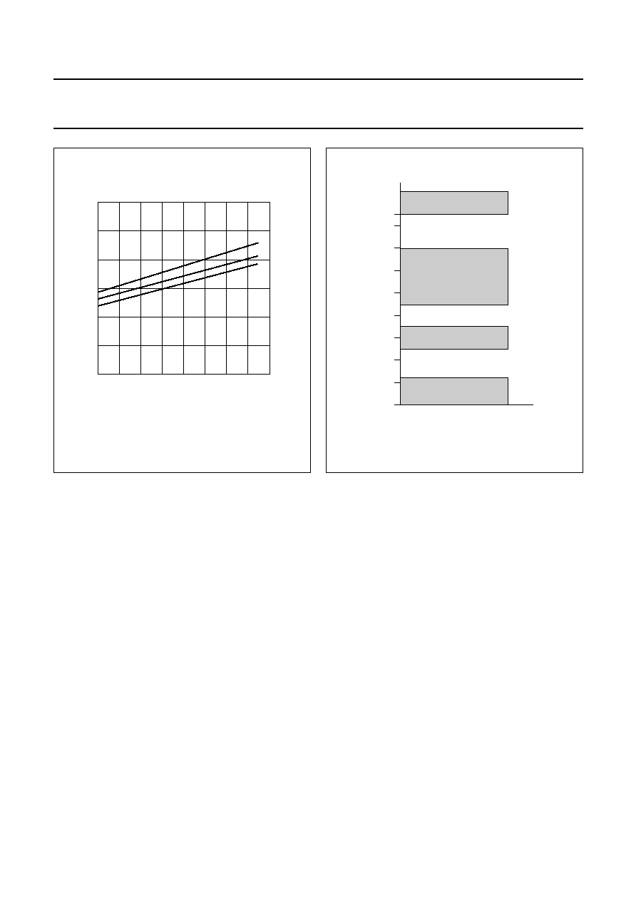
Fig.4 Switching levels of mode select switch.
handbook, halfpage
8
7
6
5
4
3
2
1
0
V16
(V)
Class - H
Class - B
Mute
Standby
MCD331 - 1
VP
8.5

1996 May 14
9
Philips Semiconductors
Product specification
40 W car radio high power amplifier
TDA1560Q
AC CHARACTERISTICS
V
P
= 14.4 V; R
L
= 8
; f
i
= 1 kHz; T
amb
= 25
∞
C and using 4 K/W heatsink; measured in Fig.6;
unless otherwise specified.
Notes
1. With a continuous sine wave input signal the output power is approximately 1 W less than driven with a bursted
signal; also depending on the equivalent series resistance of the electrolytic capacitors C1 and C2 (see Fig.6) and
the resistance of the connections between pins 5, 8, 10 and 13 and C1, C2.
2. The power bandwidth is limited by the value of the electrolytic capacitors C1 and C2.
3. Frequency response is externally fixed by the input coupling capacitor.
4. Ripple rejection measured at the output, across R
L
, with a source impedance of 0
and a frequency between 100 Hz
and 10 kHz, and an amplitude of 2 V (p-p). The maximum supply voltage ripple is 2.5 V RMS.
5. The common mode rejection ratio is measured at the output, across R
L
, with a voltage source (500 mV RMS)
between both short-circuited inputs and signal ground (see Fig.5). Frequencies are between 100 Hz and 10 kHz.
6. Noise output voltage measured in a bandwidth of 20 Hz to 20 kHz.
7. Noise output voltage independent of source impedance.
8. Input impedance without external resistor (R
ex
).
SYMBOL
PARAMETER
CONDITIONS
MIN.
TYP.
MAX.
UNIT
P
o
output power
class-H operation
THD = 0.5%
27
30
-
W
THD = 10%;
continuously driven
36
39
-
W
THD = 10%;
with burst signals; note 1
-
40
-
W
class-B operation
THD = 10%
7
10
-
W
THD
total harmonic distortion
P
o
= 1 W
-
0.05
-
%
P
o
= 10 W
-
0.1
-
%
B
power bandwidth
THD = 0.5%; P
o
=
-
1 dB
with respect to 30 W; note 2
-
40 to 15000
-
Hz
f
lr
low frequency roll-off
-
3 dB; note 3
-
40
-
Hz
f
hr
high frequency roll-off
-
1 dB
20
-
-
kHz
G
v
voltage gain
29
30
31
dB
SVRR
supply voltage ripple rejection
note 4
on
48
55
-
dB
mute
48
65
-
dB
standby
80
-
-
dB
CMRR
common mode rejection ratio
note 5
64
-
-
dB
V
i(max)
maximum input voltage
-
1.2
-
V
V
no
noise output voltage
on; R
S
= 0
; note 6
-
100
300
µ
V
on; R
S
= 10 k
; note 6
-
150
-
µ
V
mute; notes 6 and 7
-
100
-
µ
V
Z
I
input impedance
note 8
180
300
-
k

1996 May 14
10
Philips Semiconductors
Product specification
40 W car radio high power amplifier
TDA1560Q
Table 1
Values of capacitors C1, C2 and C
k
and frequency roll off
f at
-
3 dB
(Hz)
C1, C2
(
µ
F)
C
k
(nF)
10
4700
560
20
3300
270
30
2200
180
40
2200
150
50
1500
100
60
1500
82
70
1000
68
Fig.5 Common mode rejection ratio measurements.
handbook, full pagewidth
TDA1560Q
R L
output 1 ( )
output 2 ( )
ground
+VP
VP
7
11
9
6,12
input ( )
input ( )
2
3
1
MCD330 - 1

1996 May 14
11
Philips Semiconductors
Product specification
40 W car radio high power amplifier
TDA1560Q
APPLICATION INFORMATION
handbook, full pagewidth
SUPPLY
SUPPLY
TEMPERATURE
SENSOR
INPUT AND
FEEDBACK
CIRCUIT
13
10
2200 F
100 nF
2200 F
ground
9
MCD333 - 3
output 2 (+)
voltage
reference
V
POWER
STAGE
POWER
STAGE
58
2200 F
7
11
1
0.22 F
1
0.22 F
0.22 F
15
mode select switch
16
150
k
1
C
k
C
k
S1
2
4
R = 100 k
ex
150 nF
150 nF
input (+)
input
input (≠)
output 1 (≠)
15 k
10 F
10 k
17
disable
disable
V
P
V
P
12
6
V
ref
TDA1560Q
µ
2
0.22 F
µ
µ
µ
µ
150
k
µ
µ
µ
3
µ
2
0.22 F
P
LOAD DUMP
TEMPERATURE
AND CURRENT
PROTECTION
14
diagnostic
output
Fig.6 Test and application diagram.
The values for C
k
and R
ex
are given for a low frequency roll off (
-
3
dB) of 40
Hz; see also Table
1.
n this application circuit the device is driven on input pin
1.If pin
2 is used the output power will be lower.

1996 May 14
12
Philips Semiconductors
Product specification
40 W car radio high power amplifier
TDA1560Q
Fig.7 Dissipation as a function of output power.
handbook, halfpage
0
10
20
40
24
0
8
16
MLB062
30
Po (W)
Pdiss
(W)
sine wave
pink noise
Fig.8 Output power as a function of lift capacitors.
THD = 10%.
handbook, halfpage
0
2
4
8
50
40
20
0
30
MLB063
6
10
25 Hz
50 Hz
Po
(W)
C1, C2 (mF)
Fig.9 Output power as a function of frequency at THD = 1%.
handbook, full pagewidth
10
40
20
30
10
3
10
2
10
MLB064
f (Hz)
Po
(W)
11100 F
µ
8800 F
µ
6600 F
µ
4400 F
µ
2200 F
µ

1996 May 14
13
Philips Semiconductors
Product specification
40 W car radio high power amplifier
TDA1560Q
Fig.10 Output power as a function of frequency at THD = 10%.
handbook, full pagewidth
10
40
20
30
10
3
10
2
10
MLB065
f (Hz)
Po
(W)
11100 F
µ
4400 F
µ
2200 F
µ
6600 F
µ
8800 F
µ
Fig.11 Total harmonic distortion as a function of output power.
handbook, full pagewidth
0
10
20
30
40
10
2
1
MLB066
10
1
10
THD
(%)
P (W)
o
C1, C2 = 2200 F
µ
f = 10 kHz
f = 100 Hz
f = 1 kHz

1996 May 14
14
Philips Semiconductors
Product specification
40 W car radio high power amplifier
TDA1560Q
PACKAGE OUTLINE
REFERENCES
OUTLINE
VERSION
EUROPEAN
PROJECTION
ISSUE DATE
IEC
JEDEC
EIAJ
DIMENSIONS (mm are the original dimensions)
Note
1. Plastic or metal protrusions of 0.25 mm maximum per side are not included.
SOT243-1
0
5
10 mm
scale
D
L
E
A
c
A
2
L
3
Q
w
M
b
p
1
d
D
Z
e
e
x
h
1
17
j
Eh
non-concave
95-03-11
97-12-16
DBS17P: plastic DIL-bent-SIL power package; 17 leads (lead length 12 mm)
SOT243-1
view B: mounting base side
m
2
e
v
M
B
UNIT
A
e
1
A
2
b
p
c
D
(1)
E
(1)
Z
(1)
d
e
D
h
L
L
3
m
mm
17.0
15.5
4.6
4.2
0.75
0.60
0.48
0.38
24.0
23.6
20.0
19.6
10
2.54
v
0.8
12.2
11.8
1.27
e
2
5.08
2.4
1.6
E
h
6
2.00
1.45
2.1
1.8
3.4
3.1
4.3
12.4
11.0
Q
j
0.4
w
0.03
x

1996 May 14
15
Philips Semiconductors
Product specification
40 W car radio high power amplifier
TDA1560Q
SOLDERING
Introduction
There is no soldering method that is ideal for all IC
packages. Wave soldering is often preferred when
through-hole and surface mounted components are mixed
on one printed-circuit board. However, wave soldering is
not always suitable for surface mounted ICs, or for
printed-circuits with high population densities. In these
situations reflow soldering is often used.
This text gives a very brief insight to a complex technology.
A more in-depth account of soldering ICs can be found in
our
"IC Package Databook" (order code 9398 652 90011).
Soldering by dipping or by wave
The maximum permissible temperature of the solder is
260
∞
C; solder at this temperature must not be in contact
with the joint for more than 5 seconds. The total contact
time of successive solder waves must not exceed
5 seconds.
The device may be mounted up to the seating plane, but
the temperature of the plastic body must not exceed the
specified maximum storage temperature (T
stg max
). If the
printed-circuit board has been pre-heated, forced cooling
may be necessary immediately after soldering to keep the
temperature within the permissible limit.
Repairing soldered joints
Apply a low voltage soldering iron (less than 24 V) to the
lead(s) of the package, below the seating plane or not
more than 2 mm above it. If the temperature of the
soldering iron bit is less than 300
∞
C it may remain in
contact for up to 10 seconds. If the bit temperature is
between 300 and 400
∞
C, contact may be up to 5 seconds.
DEFINITIONS
LIFE SUPPORT APPLICATIONS
These products are not designed for use in life support appliances, devices, or systems where malfunction of these
products can reasonably be expected to result in personal injury. Philips customers using or selling these products for
use in such applications do so at their own risk and agree to fully indemnify Philips for any damages resulting from such
improper use or sale.
Data sheet status
Objective specification
This data sheet contains target or goal specifications for product development.
Preliminary specification
This data sheet contains preliminary data; supplementary data may be published later.
Product specification
This data sheet contains final product specifications.
Limiting values
Limiting values given are in accordance with the Absolute Maximum Rating System (IEC 134). Stress above one or
more of the limiting values may cause permanent damage to the device. These are stress ratings only and operation
of the device at these or at any other conditions above those given in the Characteristics sections of the specification
is not implied. Exposure to limiting values for extended periods may affect device reliability.
Application information
Where application information is given, it is advisory and does not form part of the specification.

Philips Semiconductors ≠ a worldwide company
Argentina: see South America
Australia: 34 Waterloo Road, NORTH RYDE, NSW 2113,
Tel. (02) 805 4455, Fax. (02) 805 4466
Austria: Computerstr. 6, A-1101 WIEN, P.O. Box 213,
Tel. (01) 60 101-1256, Fax. (01) 60 101-1250
Belarus: Hotel Minsk Business Center, Bld. 3, r. 1211,
Volodarski Str. 6, 220050 MINSK,
Tel. (172) 200 733, Fax. (172) 200 773
Belgium: see The Netherlands
Brazil: see South America
Bulgaria: Philips Bulgaria Ltd., Energoproject, 15th floor,
51 James Bourchier Blvd., 1407 SOFIA,
Tel. (359) 2 689 211, Fax. (359) 2 689 102
Canada: PHILIPS SEMICONDUCTORS/COMPONENTS:
Tel. (800) 234-7381, Fax. (708) 296-8556
Chile: see South America
China/Hong Kong: 501 Hong Kong Industrial Technology Centre,
72 Tat Chee Avenue, Kowloon Tong, HONG KONG,
Tel. (852) 2319 7888, Fax. (852) 2319 7700
Colombia: see South America
Czech Republic: see Austria
Denmark: Prags Boulevard 80, PB 1919, DK-2300
COPENHAGEN S, Tel. (032) 88 2636, Fax. (031) 57 1949
Finland: Sinikalliontie 3, FIN-02630 ESPOO,
Tel. (358) 0-615 800, Fax. (358) 0-61580 920
France: 4 Rue du Port-aux-Vins, BP317,
92156 SURESNES Cedex,
Tel. (01) 4099 6161, Fax. (01) 4099 6427
Germany: P.O. Box 10 51 40, 20035 HAMBURG,
Tel. (040) 23 53 60, Fax. (040) 23 53 63 00
Greece: No. 15, 25th March Street, GR 17778 TAVROS,
Tel. (01) 4894 339/4894 911, Fax. (01) 4814 240
Hungary: see Austria
India: Philips INDIA Ltd, Shivsagar Estate, A Block,
Dr. Annie Besant Rd. Worli, BOMBAY 400 018
Tel. (022) 4938 541, Fax. (022) 4938 722
Indonesia: see Singapore
Ireland: Newstead, Clonskeagh, DUBLIN 14,
Tel. (01) 7640 000, Fax. (01) 7640 200
Israel: RAPAC Electronics, 7 Kehilat Saloniki St, TEL AVIV 61180,
Tel. (03) 645 04 44, Fax. (03) 648 10 07
Italy: PHILIPS SEMICONDUCTORS,
Piazza IV Novembre 3, 20124 MILANO,
Tel. (0039) 2 6752 2531, Fax. (0039) 2 6752 2557
Japan: Philips Bldg 13-37, Kohnan 2-chome, Minato-ku,
TOKYO 108, Tel. (03) 3740 5130, Fax. (03) 3740 5077
Korea: Philips House, 260-199 Itaewon-dong,
Yongsan-ku, SEOUL, Tel. (02) 709-1412, Fax. (02) 709-1415
Malaysia: No. 76 Jalan Universiti, 46200 PETALING JAYA,
SELANGOR, Tel. (03) 750 5214, Fax. (03) 757 4880
Mexico: 5900 Gateway East, Suite 200, EL PASO,
TEXAS 79905, Tel. 9-5(800) 234-7831, Fax. (708) 296-8556
Middle East: see Italy
Netherlands: Postbus 90050, 5600 PB EINDHOVEN, Bldg. VB,
Tel. (040) 2783749, Fax. (040) 2788399
New Zealand: 2 Wagener Place, C.P.O. Box 1041, AUCKLAND,
Tel. (09) 849-4160, Fax. (09) 849-7811
Norway: Box 1, Manglerud 0612, OSLO,
Tel. (022) 74 8000, Fax. (022) 74 8341
Philippines: PHILIPS SEMICONDUCTORS PHILIPPINES Inc.,
106 Valero St. Salcedo Village, P.O. Box 2108 MCC,
MAKATI, Metro MANILA,
Tel. (63) 2 816 6380, Fax. (63) 2 817 3474
Poland: Ul. Lukiska 10, PL 04-123 WARSZAWA,
Tel. (022) 612 2831, Fax. (022) 612 2327
Portugal: see Spain
Romania: see Italy
Singapore: Lorong 1, Toa Payoh, SINGAPORE 1231,
Tel. (65) 350 2000, Fax. (65) 251 6500
Slovakia: see Austria
Slovenia: see Italy
South Africa: S.A. PHILIPS Pty Ltd.,
195-215 Main Road Martindale, 2092 JOHANNESBURG,
P.O. Box 7430 Johannesburg 2000,
Tel. (011) 470-5911, Fax. (011) 470-5494
South America: Rua do Rocio 220 - 5th floor, Suite 51,
CEP: 04552-903-S√O PAULO-SP, Brazil,
P.O. Box 7383 (01064-970),
Tel. (011) 821-2333, Fax. (011) 829-1849
Spain: Balmes 22, 08007 BARCELONA,
Tel. (03) 301 6312, Fax. (03) 301 4107
Sweden: Kottbygatan 7, Akalla. S-16485 STOCKHOLM,
Tel. (0) 8-632 2000, Fax. (0) 8-632 2745
Switzerland: Allmendstrasse 140, CH-8027 ZÐRICH,
Tel. (01) 488 2211, Fax. (01) 481 77 30
Taiwan: PHILIPS TAIWAN Ltd., 23-30F, 66,
Chung Hsiao West Road, Sec. 1, P.O. Box 22978,
TAIPEI 100, Tel. (886) 2 382 4443, Fax. (886) 2 382 4444
Thailand: PHILIPS ELECTRONICS (THAILAND) Ltd.,
209/2 Sanpavuth-Bangna Road Prakanong, BANGKOK 10260,
Tel. (66) 2 745-4090, Fax. (66) 2 398-0793
Turkey: Talatpasa Cad. No. 5, 80640 GÐLTEPE/ISTANBUL,
Tel. (0212) 279 2770, Fax. (0212) 282 6707
Ukraine: PHILIPS UKRAINE,
2A Akademika Koroleva str., Office 165, 252148 KIEV,
Tel. 380-44-4760297, Fax. 380-44-4766991
United Kingdom: Philips Semiconductors LTD.,
276 Bath Road, Hayes, MIDDLESEX UB3 5BX,
Tel. (0181) 730-5000, Fax. (0181) 754-8421
United States: 811 East Arques Avenue, SUNNYVALE,
CA 94088-3409, Tel. (800) 234-7381, Fax. (708) 296-8556
Uruguay: see South America
Vietnam: see Singapore
Yugoslavia: PHILIPS, Trg N. Pasica 5/v, 11000 BEOGRAD,
Tel. (381) 11 825 344, Fax. (359) 211 635 777
Internet: http://www.semiconductors.philips.com/ps/
For all other countries apply to: Philips Semiconductors,
Marketing & Sales Communications, Building BE-p,
P.O. Box 218, 5600 MD EINDHOVEN, The Netherlands,
Fax. +31-40-2724825
SCDS48
© Philips Electronics N.V. 1996
All rights are reserved. Reproduction in whole or in part is prohibited without the
prior written consent of the copyright owner.
The information presented in this document does not form part of any quotation
or contract, is believed to be accurate and reliable and may be changed without
notice. No liability will be accepted by the publisher for any consequence of its
use. Publication thereof does not convey nor imply any license under patent- or
other industrial or intellectual property rights.
Printed in The Netherlands
517021/1200/04/pp16
Date of release: 1996 May 14
Document order number:
9397 750 00844