Document Outline
- GENERAL DESCRIPTION
- Features
- QUICK REFERENCE DATA
- PACKAGE OUTLINE
- Block diagram
- FUNCTIONAL DESCRIPTION
- RATINGS
- THERMAL RESISTANCE
- CHARACTERISTICS
- APPLICATION INFORMATION
- PACKAGE OUTLINE
- SOLDERING
- DEFINITIONS
- LIFE SUPPORT APPLICATIONS

DATA SHEET
Product specification
File under Integrated Circuits, IC01
February 1985
INTEGRATED CIRCUITS
TDA1574
Integrated FM tuner for radio
receivers

February 1985
2
Philips Semiconductors
Product specification
Integrated FM tuner for radio receivers
TDA1574
GENERAL DESCRIPTION
The TDA1574 is a monolithic integrated FM tuner circuit designed for use in the r.f./i.f. section of car radios and
home-receivers. The circuit comprises a mixer, oscillator and a linear i.f. amplifier for signal processing, plus the following
additional features.
Features
∑
Keyed automatic gain control (a.g.c.)
∑
Regulated reference voltage
∑
Buffered oscillator output
∑
Electronic standby switch
∑
Internal buffered mixer driving.
QUICK REFERENCE DATA
PACKAGE OUTLINE
18-lead DIL; plastic (SOT102); SOT102-1; 1996 August 08.
Supply voltage range (pin 15)
V
P
7 to 16 V
Mixer input bias voltage (pins 1 and 2)
V
1, 2-4
typ.
1 V
noise figure
NF
typ.
9 dB
Oscillator output voltage (pin 6)
V
6-4
typ.
2 V
output admittance at pin 6 for f = 108,7 MHz
Y22
typ.
1,5
+
j2 mS
Oscillator output buffer
D.C. output voltage (pin 9)
V
9-4
typ.
6 V
Total harmonic distortion
THD
typ.
-
15 dBC
Linear i.f. amplifier output voltage (pin 10)
V
10-4
typ.
4,5 V
noise figure at R
S
= 300
NF
typ.
6,5 dB
Keyed a.g.c. output voltage range (pin 18)
V
18-4
+
0,5 to V
P
-
0,3 V

February 1985
3
Philips Semiconductors
Product specification
Integrated FM tuner for radio receivers
TDA1574
This text is here in white to force landscape pages to be rotated correctly when browsing through the pdf in the Acrobat reader.This text is here in
_
white to force landscape pages to be rotated correctly when browsing through the pdf in the Acrobat reader.This text is here inThis text is here in
white to force landscape pages to be rotated correctly when browsing through the pdf in the Acrobat reader. white to force landscape pages to be ...
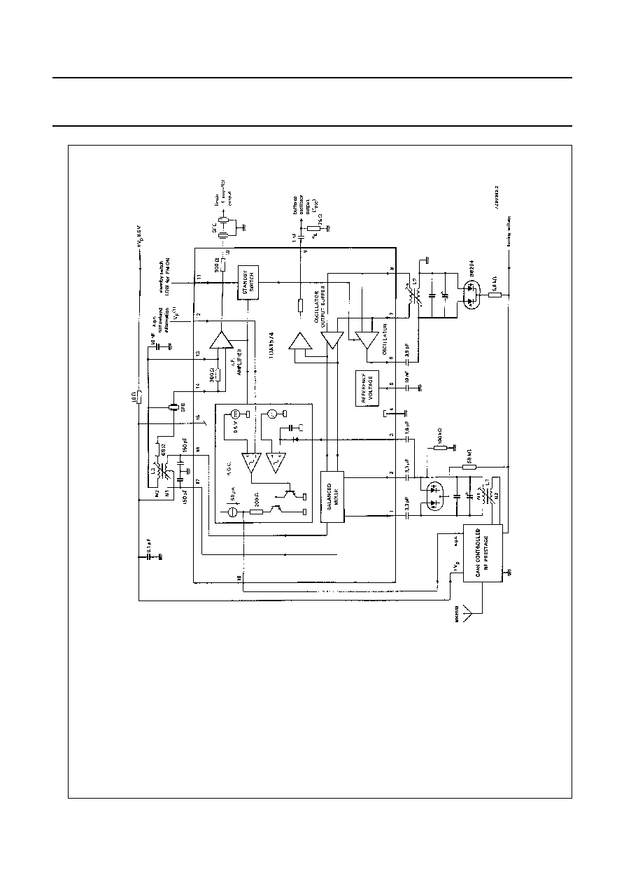
Fig.1 Block diagram and test circuit.
Coil data
L1: TOKO MC-108, 514HNE-150014S14; L = 0,078
µ
H
L2: TOKO MC-111, E516HNS-200057; L = 0,08
µ
H
L3: TOKO coil set 7P, N1 = 5,5
+
5,5 turns, N2 = 4 turns

February 1985
4
Philips Semiconductors
Product specification
Integrated FM tuner for radio receivers
TDA1574
FUNCTIONAL DESCRIPTION
Mixer
The mixer circuit is a double balanced multiplier with a preamplifier (common base input) to obtain a large signal handling
range and a low oscillator radiation.
Oscillator
The oscillator circuit is an amplifier with a differential input. Voltage regulation is achieved by utilizing the symmetrical
tanh-transfer-function to obtain low order 2nd harmonics.
Linear IF amplifier
The IF amplifier is a one stage, differential input, wideband amplifier with an output buffer.
Keyed AGC
The AGC processor combines narrow- and wideband information via an RF level detector, a comparator and an ANDing
stage. The level dependent, current sinking output has an active load, which sets the AGC threshold.
The AGC function can either be controlled by a combination of wideband and narrowband information (keyed AGC), or
by a wideband information only, or by narrowband information only. If only narrow-band AGC is wanted pin 3 should be
connected to pin 5. If only wideband AGC is wanted pin 12 should be connected to pin 13.
RATINGS
Limiting values in accordance with the Absolute Maximum System (IEC 134)
THERMAL RESISTANCE
Note
All pins are short-circuit protected to ground.
Supply voltage (pin 15)
V
P
= V
15-4
max.
18 V
Mixer output voltage (pins 16 and 17)
V
16, 17-4
max.
35 V
Standby switch input voltage (pin 11)
V
11-4
max.
23 V
Reference voltage (pin 5)
V
5-4
max.
7 V
Field strength input voltage (pin 12)
V
12-4
max.
7 V
Total power dissipation
P
tot
max.
800 mW
Storage temperature range
T
stg
-
55 to
+
150
∞
C
Operating ambient temperature range
T
amb
-
40 to
+
85
∞
C
From junction to ambient (in free air)
R
th j-amb
=
80 K/W

February 1985
5
Philips Semiconductors
Product specification
Integrated FM tuner for radio receivers
TDA1574
CHARACTERISTICS
V
P
= V
15-4
= 8,5 V; T
amb
= 25
∞
C; measured in test circuit Fig.1; unless otherwise specified
PARAMETER
SYMBOL
MIN.
TYP.
MAX.
UNIT
Supply (pin 15)
Supply voltage
V
P
= V
15-4
7
-
16
V
Supply current (except mixer)
I
P
= I
15
16
23
30
mA
Reference voltage (pin 5)
V
5-4
3,9
4,1
4,4
V
Mixer
D.C. characteristics
Input bias voltage (pins 1 and 2)
V
1,2-4
-
1
-
V
Output voltage (pins 16 and 17)
V
16,17-4
4
-
35
V
Output current (pin 16
+
pin 17)
I
16
+
I
17
-
4,0
-
mA
A.C. characteristics (f
i
= 98 MHz)
Noise figure
NF
-
9
-
dB
Noise figure including transforming network
NF
-
11
-
dB
3rd order intercept point
EMF1
IP3
-
115
-
dB
µ
V
Conversion power gain
G
P
-
14
-
dB
Input resistance (pins 1 and 2)
R
1,2-4
-
14
-
Output capacitance (pins 16 and 17)
C
16,17
-
13
-
pF
Oscillator
D.C. characteristics
Input voltage (pins 7 and 8)
V
7,8-4
-
1,3
-
V
Output voltage (pin 6)
V
6-4
-
2
-
V
A.C. characteristics (f
osc
= 108,7 MHz)
Residual FM (Bandwidth 300 Hz to 15 kHz);
de-emphasis = 50
µ
s
f
-
2,2
-
Hz
10
4 V
M out
(
)
10 7 MHz
,
(
)
EMF1 98 MHz
(
)
2
----------------------------------------------------------
2
R
S1
R
ML
-----------
◊
log

February 1985
6
Philips Semiconductors
Product specification
Integrated FM tuner for radio receivers
TDA1574
Linear i.f. amplifier
D.C. characteristics
Input bias voltage (pin 13)
V
13-4
-
1,2
-
V
Output voltage (pin 10)
V
10-4
-
4,5
-
V
A.C. characteristics (f
i
= 10,7 MHz)
Input impedance
R
14-13
240
300
360
C
14-13
-
13
-
pF
Output impedance
R
10-4
240
300
360
C
10-4
-
3
-
pF
Voltage gain
G
VIF
27
30
-
dB
T
amb
=
-
40 to
+
85
∞
C
G
VIF
-
0
-
dB
1 dB compression point (r.m.s. value)
at V
P
= 8,5 V
V
10-4rms
-
750
-
mV
at V
P
= 7,5 V
V
10-4rms
-
550
-
mV
Noise figure
at R
S
= 300
NF
-
6,5
-
dB
Keyed a.g.c.
D.C. characteristics
Output voltage range (pin 18)
V
18-4
0,5
-
V
P-0,3
V
A.G.C. output current
at I
3
=
or
V
12-4
= 450 mV; V
18-4
= V
P
/2
-
I
18
25
50
100
µ
A
at V
3-4
= 2 V and
V
12-4
= 1 V; V
18-4
= V
15-4
I
18
2
-
5
mA
PARAMETER
SYMBOL
MIN.
TYP.
MAX.
UNIT
20
V
10
4
≠
V
14
13
≠
------------------
log

February 1985
7
Philips Semiconductors
Product specification
Integrated FM tuner for radio receivers
TDA1574
Narrowband threshold
at V
3-4
= 2 V; V
12-4
= 550 mV
V
18-4
-
-
1
V
at V
3-4
= 2 V; V
12-4
= 450 mV
V
18-4
V
P-0,3
-
-
V
A.C. characteristics (f
i
= 98 MHz)
Input impedance
R
3-4
-
4
-
k
C
3-4
-
3
-
pF
Wideband threshold (r.m.s. value)
(see figures 2, 3, 4 and 5)
at V
12-4
= 0,7 V; V
18-4
= V
P
/2; I
18
= 0
EMF2
rms
-
17
-
mV
Oscillator output buffer (pin 9)
D.C. output voltage
V
9-4
-
6,0
-
V
Oscillator output voltage (r.m.s. value)
at R
L
=
; C
L
= 2 pF
V
9-4(rms)
-
110
-
mV
at R
L
= 75
V
9-4(rms)
30
50
-
mV
D.C. output impedance
R
9-15
-
2,5
-
k
Signal purity
Total harmonic distortion
THD
-
-
15
-
dBC
Spurious frequencies
at EMF1 = 0,2 V; R
S1
= 50
f
S
-
-
35
-
dBC
Electronic standby switch (pin 11 )
Oscillator; linear i.f. amplifier; a.g.c.
at T
amb
=
-
40 to
+
85
∞
C
Input switching voltage
for threshold ON; V
18-4
=
V
P
-
3 V
V
11-4
0
-
2,3
V
for threshold OFF; V
18-4
=
0,5 V
V
11-4
3,3
-
23
V
Input current
at ON condition; V
11-4
= 0 V
-
I
11
-
-
150
µ
A
at OFF condition; V
11-4
= 23 V
I
11
-
-
10
µ
A
Input voltage
at I
11
=
V
11-4
-
-
4,4
V
PARAMETER
SYMBOL
MIN.
TYP.
MAX.
UNIT

February 1985
8
Philips Semiconductors
Product specification
Integrated FM tuner for radio receivers
TDA1574
Fig.2
Keyed a.g.c. output voltage V
18-4
as a
function of r.m.s. input voltage V
3-4.
Measured in test circuit Fig.1 at
V
12-4
= 0,7 V; I
18
=
.
Fig.3
Keyed a.g.c. output voltage V
18-4
as a function of input voltage V
12-4
.
Measured in test circuit Fig.1 at
V
3-4
= 2 V; I
18
=
.
Fig.4
Keyed a.g.c. output current I
18
as a
function of r.m.s. input voltage V
3-4.
Measured in test circuit Fig.1 at
V
12-4
= 0,7 V; V
18-4
= 8,5 V.
Fig.5
Keyed a.g.c. output current I
18
as a
function of input voltage V
12-4
.
Measured in test circuit Fig.1 at
V
3-4
= 2 V; V
18-4
= 8,5 V.
February 1985
9
Philips Semiconductors
Product specification
Integrated FM tuner for radio receivers
TDA1574
This text is here in white to force landscape pages to be rotated correctly when browsing through the pdf in the Acrobat reader.This text is here in
_
white to force landscape pages to be rotated correctly when browsing through the pdf in the Acrobat reader.This text is here inThis text is here in
white to force landscape pages to be rotated correctly when browsing through the pdf in the Acrobat reader. white to force landscape pages to be ...
APPLICATION INFORMATION
Coil data
L1 :
TOKO MC-108,
514HNE-15023S15,
N1 = 5,5 turns, N2 = 1
turn
L2:
see Fig.1
L3:
(1) Field strength indication
of main i.f. amplifier.
Fig.6 TDA1574 application diagram.

February 1985
10
Philips Semiconductors
Product specification
Integrated FM tuner for radio receivers
TDA1574
PACKAGE OUTLINE
REFERENCES
OUTLINE
VERSION
EUROPEAN
PROJECTION
ISSUE DATE
IEC
JEDEC
EIAJ
SOT102-1
93-10-14
95-01-23
UNIT
A
max.
1
2
b
1
(1)
(1)
(1)
b
2
c
D
E
e
M
Z
H
L
mm
DIMENSIONS (inch dimensions are derived from the original mm dimensions)
A
min.
A
max.
b
max.
w
M
E
e
1
1.40
1.14
0.53
0.38
0.32
0.23
21.8
21.4
6.48
6.20
3.9
3.4
0.254
2.54
7.62
8.25
7.80
9.5
8.3
0.85
4.7
0.51
3.7
inches
0.055
0.044
0.021
0.015
0.013
0.009
1.40
1.14
0.055
0.044
0.86
0.84
0.26
0.24
0.15
0.13
0.01
0.10
0.30
0.32
0.31
0.37
0.33
0.033
0.19
0.020
0.15
M
H
c
(e )
1
M
E
A
L
seating plane
A
1
w
M
b
1
b
2
e
D
A
2
Z
18
1
10
9
b
E
pin 1 index
0
5
10 mm
scale
Note
1. Plastic or metal protrusions of 0.25 mm maximum per side are not included.
DIP18: plastic dual in-line package; 18 leads (300 mil)
SOT102-1

February 1985
11
Philips Semiconductors
Product specification
Integrated FM tuner for radio receivers
TDA1574
SOLDERING
Introduction
There is no soldering method that is ideal for all IC
packages. Wave soldering is often preferred when
through-hole and surface mounted components are mixed
on one printed-circuit board. However, wave soldering is
not always suitable for surface mounted ICs, or for
printed-circuits with high population densities. In these
situations reflow soldering is often used.
This text gives a very brief insight to a complex technology.
A more in-depth account of soldering ICs can be found in
our
"IC Package Databook" (order code 9398 652 90011).
Soldering by dipping or by wave
The maximum permissible temperature of the solder is
260
∞
C; solder at this temperature must not be in contact
with the joint for more than 5 seconds. The total contact
time of successive solder waves must not exceed
5 seconds.
The device may be mounted up to the seating plane, but
the temperature of the plastic body must not exceed the
specified maximum storage temperature (T
stg max
). If the
printed-circuit board has been pre-heated, forced cooling
may be necessary immediately after soldering to keep the
temperature within the permissible limit.
Repairing soldered joints
Apply a low voltage soldering iron (less than 24 V) to the
lead(s) of the package, below the seating plane or not
more than 2 mm above it. If the temperature of the
soldering iron bit is less than 300
∞
C it may remain in
contact for up to 10 seconds. If the bit temperature is
between 300 and 400
∞
C, contact may be up to 5 seconds.
DEFINITIONS
LIFE SUPPORT APPLICATIONS
These products are not designed for use in life support appliances, devices, or systems where malfunction of these
products can reasonably be expected to result in personal injury. Philips customers using or selling these products for
use in such applications do so at their own risk and agree to fully indemnify Philips for any damages resulting from such
improper use or sale.
Data sheet status
Objective specification
This data sheet contains target or goal specifications for product development.
Preliminary specification
This data sheet contains preliminary data; supplementary data may be published later.
Product specification
This data sheet contains final product specifications.
Limiting values
Limiting values given are in accordance with the Absolute Maximum Rating System (IEC 134). Stress above one or
more of the limiting values may cause permanent damage to the device. These are stress ratings only and operation
of the device at these or at any other conditions above those given in the Characteristics sections of the specification
is not implied. Exposure to limiting values for extended periods may affect device reliability.
Application information
Where application information is given, it is advisory and does not form part of the specification.