 | –≠–ª–µ–∫—Ç—Ä–æ–Ω–Ω—ã–π –∫–æ–º–ø–æ–Ω–µ–Ω—Ç: TDA2579C | –°–∫–∞—á–∞—Ç—å:  PDF PDF  ZIP ZIP |
Document Outline
- FEATURES
- Synchronization and horizontal part
- Vertical part
- GENERAL DESCRIPTION
- ORDERING INFORMATION
- QUICK REFERENCE DATA
- PINNING
- FUNCTIONAL DESCRIPTION
- Vertical part (pins 1, 2, 3 and 4)
- Divider system
- Vertical sawtooth
- Vertical feedback
- Vertical guard
- Vertical driver output
- Integration time of the vertical synchronization pulse separator
- Sync separator, phase detector and TV-station identification (pins 5, 6, 7 and 18)
- Explanation of areas A to G shown in Fig.3
- Supply (pins 9, 10 and 16)
- Horizontal oscillator, horizontal output transistor and second phase detector
- Mute output and 60 Hz identification (pin 13)
- Sandcastle output (pin 17)
- LIMITING VALUES
- THERMAL RESISTANCE
- CHARACTERISTICS
- PACKAGE OUTLINE
- SOLDERING
- DEFINITIONS
- LIFE SUPPORT APPLICATIONS

DATA SHEET
Preliminary specification
File under Integrated Circuits, IC02
January 1994
INTEGRATED CIRCUITS
Philips Semiconductors
TDA2579C
Synchronization circuit with
synchronized vertical divider
system for 60 Hz

January 1994
2
Philips Semiconductors
Preliminary specification
Synchronization circuit with synchronized
vertical divider system for 60 Hz
TDA2579C
FEATURES
Synchronization and horizontal part
∑
Horizontal sync separator and noise inverter
∑
Horizontal oscillator
∑
Horizontal output stage
∑
Horizontal phase detector (sync to oscillator)
∑
Triple current source in the phase detector with
automatic selection
∑
Normal phase detector time constant is increased to fast
during the vertical blanking period (external switching for
VTR conditions not necessary)
∑
Slow phase detector time constant and gated sync pulse
operation are automatically switched on by an internal
sync pulse noise level detection circuit
∑
Fast phase detector time is switched on for locking
∑
Time constant externally switchable
∑
Inhibit of horizontal phase detector and video transmitter
identification circuit during equalizing pulses and vertical
sync pulse
∑
Inhibit of horizontal phase detector during separated
vertical sync pulse
∑
Second phase detector for storage compensation of the
line output stage
∑
3-level sandcastle pulse generator
∑
Automatic adaption of the burst key pulse width
∑
Video transmitter identification circuit
∑
Stabilizer and supply circuit for starting the horizontal
oscillator and output stage directly from the mains
rectifier
∑
Horizontal output current with constant duty factor value
of 55%
∑
Duty factor of the horizontal output pulse is 55% when
the horizontal flyback pulse is absent.
Vertical part
∑
f
V
= 60 Hz (M) system
∑
Vertical synchronization pulse separator without
external components and two integration times
∑
Zener diode reference voltage source for the vertical
sawtooth generator and vertical comparator
∑
Divider system with three different reset enable windows
∑
Synchronization is set to 528 divider ratio when no
vertical sync pulse and no video transmitter is identified
∑
Divider window is forced to wide window when a vertical
sync pulse is detected within the window provided by
reset divider and end of vertical blanking period, on
condition that the voltage on pin 18 is
1.2 V
∑
Divider ratio is 528 (f
V
= 60 Hz) for DC signal on pin 5
∑
Linear negative-going sawtooth generated via the
divider system (no frequency adjustment)
∑
Comparator with low DC level feedback signal
∑
Output stage driver
∑
f
V
= 60 Hz identification output combined with mute
function
∑
Start of vertical blanking is shifted to the start of the
pre-equalizing pulses when the divider ratio is between
522 and 528 lines per picture
∑
Guard circuit which generates the vertical blanking
pulse level on the sandcastle output pin 17 when the
feedback level at pin 2 is not within the specified limits.
GENERAL DESCRIPTION
The TDA2579C is an integrated circuit generating all
requirements for synchronization of its horizontal oscillator
and output stage plus those of the vertical part which
comprises a divider system, sawtooth generator,
comparator and output stage.
The TDA2579C is almost identical to the TDA2579B.
It is optimized for the M (60 Hz) TV system.
ORDERING INFORMATION
EXTENDED TYPE
NUMBER
PACKAGE
PINS
PIN POSITION
MATERIAL
CODE
TDA2579C
18
DIL
plastic
SOT102

January 1994
3
Philips Semiconductors
Preliminary specification
Synchronization circuit with synchronized
vertical divider system for 60 Hz
TDA2579C
QUICK REFERENCE DATA
Note
1. Open collector loaded with external resistor to positive supply.
SYMBOL
PARAMETER
CONDITIONS
MIN.
TYP.
MAX.
UNIT
Supply
I
16
minimum required current for starting
horizontal oscillator and output stage
6.2
-
-
mA
V
10
main supply voltage
-
12
-
V
I
10
supply current
-
70
-
mA
Input signals
V
5-9
sync pulse input amplitude
0.05
-
1
V
I
12
horizontal flyback pulse input current
0.2
1
-
mA
V
2
vertical comparator input voltage
AC (peak-to-peak value)
-
0.8
-
V
DC
-
1
-
V
Output signals
V
11
horizontal output voltage
(open collector)
I
11
= 25 mA
-
-
0.5
V
V
1
vertical output stage driver
(emitter follower)
I
1
= 1.5 mA
5
-
-
V
V
17
sandcastle output voltage levels
burst key
9.8
-
-
V
horizontal blanking
-
4.5
-
V
vertical blanking
-
2.5
-
V
V
IDEO TRANSMITTER IDENTIFICATION OUTPUT
; note 1
V
13
output voltage
no sync pulse present
-
-
0.32
V
I
13
output current
no sync pulse present
-
-
5
mA
V
13
output voltage
sync pulse present;
divider ratio <576
-
7.6
-
V

January 1994
4
Philips Semiconductors
Preliminary specification
Synchronization circuit with synchronized
vertical divider system for 60 Hz
TDA2579C
MGA791
1
nF
9
100 nF
VERTICAL/
HORIZONTAL
SYNC
SEPARATOR
NOISE
INVERTER
COINCIDENCE
DETECTOR
PHASE
DETECTOR
1
GATING
DIVIDER
VERTICAL
ZENER
REFERENCE
VERTICAL
COMPARATOR
SYNC PULSE
NOISE LEVEL
DETECTOR
1
REFERENCE
VERTICAL
BLANKING
VERTICAL
GUARD
CIRCUIT
VERTICAL
OUTPUT
NOISE
DETECTOR
ANTITOP
BURST
KEY
SANDCASTLE
OUTPUT
HORIZONTAL
OSCILLATOR
2
REFERENCE
FLYBACK
PULSE
PROTECTION
PULSE
WIDTH
MODULATOR
PHASE
DETECTOR
2
TOO LOW
CURRENT
PROTECTION
HORIZONTAL
OUTPUT
SUPPLY
SWITCH
START
CIRCUIT
STABILIZER
VIDEO
TRANSMITTER
IDENTIFICATION
VERTICAL/
OSCILLATOR
SAWTOOTH
GENERATOR
12
10
16
15
8
5
13
18
7
6
11
4.7 nF
6.8 k
horizontal
drive
to pin 16
220 k
TDA2579C
flyback pulse
input
sandcastle
output
vertical
drive
vertical
feedback
150 nF
150 k
to vertical deflection
current measuring resistor
43
2
1
1
7
22
µ
F
I 6.2 mA
68 nF
150 pF
6.8
µ
F
1 k
1.2 k
video
signal
input
22
µ
F
22
5.6 k
2.2
µ
F
47 nF
15 k
mute
60 Hz
12 V
33 k
4.7 k
2.7 nF
12 V
14
R =
S
Fig.1 Block diagram.
January 1994
5
Philips Semiconductors
Preliminary specification
Synchronization circuit with synchronized
vertical divider system for 60 Hz
TDA2579C
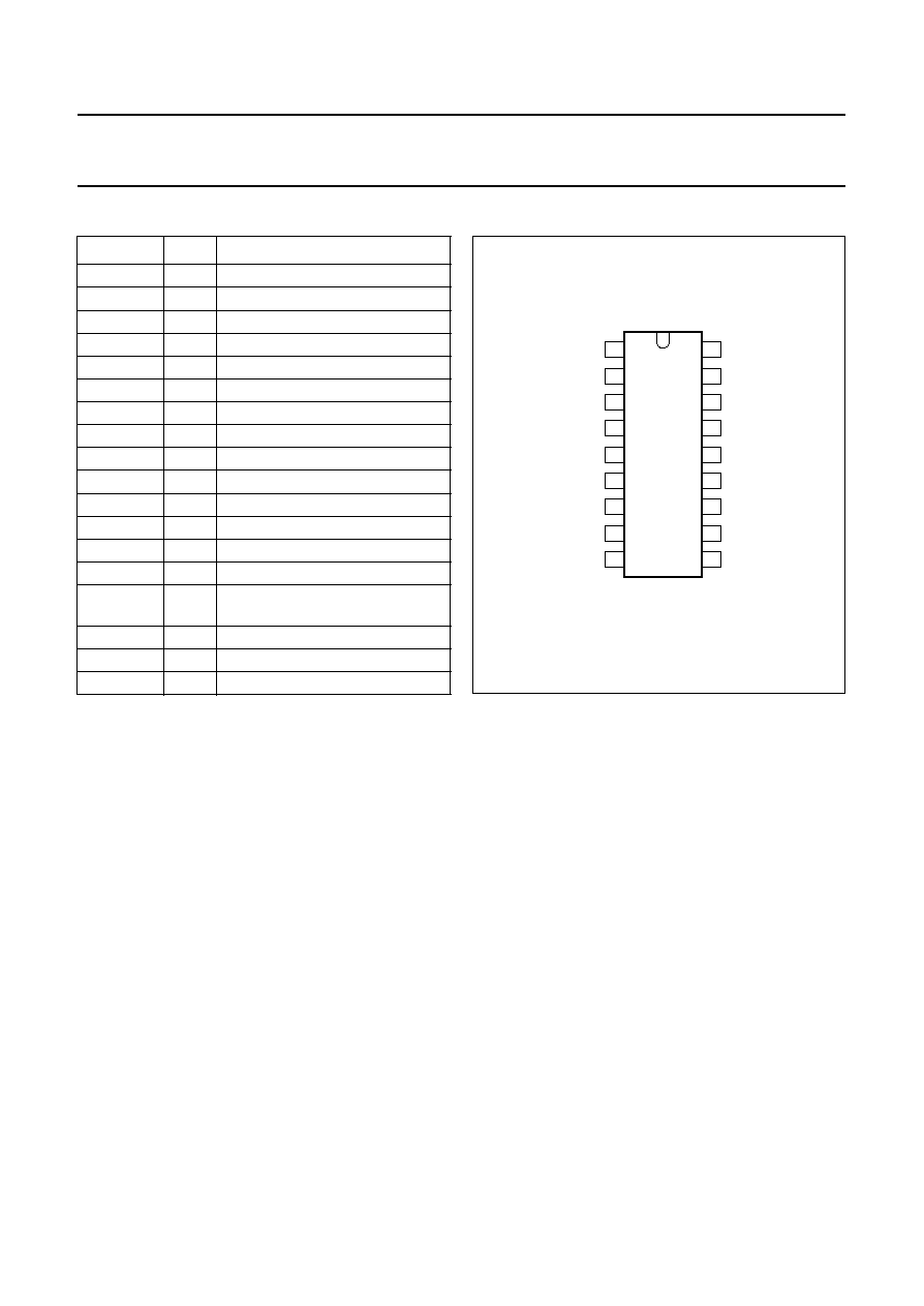
PINNING
SYMBOL
PIN
DESCRIPTION
V
OUT
1
vertical driver output
FB
2
vertical feedback input
SAW
3
vertical sawtooth generator
VDC
4
vertical deflection current output
VID
5
video signal input
CSL
6
slicing level storage capacitor
RSL
7
slicing level resistor
1
8
phase detector
1
GND
9
ground (0 V)
V
P
10
main supply voltage (+12 V)
H
OUT
11
horizontal driver output
FLYB
12
horizontal flyback pulse input
MUTE
13
mute output
H
SHIFT
14
horizontal picture shift capacitor
H
OSC
15
horizontal oscillator frequency
setting
STAB
16
start circuit stabilizer input
SC
17
sandcastle output
DET
18
coincidence detector output
Fig.2 Pin configuration.
1
2
3
4
5
6
7
8
9
18
17
16
15
14
13
12
11
10
MGA790
V
FB
SAW
VDC
VID
CSL
RSL
1
GND
DET
SC
STAB
H
SHIFT
MUTE
FLYB
H
VP
TDA2579C
OSC
OUT
H
OUT
FUNCTIONAL DESCRIPTION
The TDA2579C generates both horizontal and vertical
drive signals, a 3-level sandcastle output pulse, a
transmitter identification signal and 60 Hz window
information.
The horizontal oscillator and horizontal output stage
functions are started via the supply current into pin 16.
The required current has a typical value of 5 mA which can
be taken directly from the mains rectifier. The horizontal
output transistor at pin 11 is not conducting until the supply
current at pin 16 has reached its typical value. The starting
circuit has a hysteresis of approximately 1 mA. The
horizontal output current of pin 11 starts at a duty cycle of
60%. All other IC functions are enabled via the main supply
voltage on pin 10.
The pin 16 supply system enables slaved synchronized
switch mode systems in which the horizontal output signal
of the TDA2579C is used as master signal. In such a
system the 12 V supply (main supply at pin 10) can be
generated by the line output stage.
An internal Zener diode reference voltage is used for the
vertical processing part. The IC embodies a synchronized
divider system for generating the vertical sawtooth at
pin 3. Thus no vertical frequency adjustment is required.
The circuit operation is restricted to the M (f
V
= 60 Hz)
system.
Vertical part (pins 1, 2, 3 and 4)
The IC embodies a synchronized divider system for
generating the vertical sawtooth at pin 3. The divider
system has an internal frequency doubling circuit, thus the
horizontal oscillator is operating at its nominal line
frequency and one line period equals 2 clock pulses.
No vertical frequency adjustment is required due to the
divider system. The divider system operates with
3 different reset windows for maximum
interference/disturbance protection.
The windows are activated via an up/down counter.
The counter increases its value by 1 each time the
separated vertical sync pulse is within the window being
searched. The count is reduced by 1 when the vertical
sync pulse is not present.
The reset of the counter system (clock pulse 0) is at half a
line period after the start of the vertical pulse at pin 5.

January 1994
6
Philips Semiconductors
Preliminary specification
Synchronization circuit with synchronized
vertical divider system for 60 Hz
TDA2579C
In accordance with the convention for the M system, field
one line 1 number 1 starts at the first equalizing pulse, the
reset of the divider system is at the start of line 4 for the first
field and in the middle of line 265 for the second field.
Divider system
M
ODE
A:
LARGE
(
SEARCH
)
WINDOW
Divider ratio between 488 and 576.
This mode is valid for the following five conditions:
1. Divider is locking to a new transmitter.
2. Divider ratio found, not being within the narrow window
limits.
3. Up/down counter value of the divider system operating
in the narrow window mode decreases below count 1.
4. External forced setting. This can be achieved by
loading pin 18 with a 220
resistor to earth or by
connecting a 3.6 V stabistor diode between pin 18 and
ground.
5. A vertical sync pulse was detected within the interval
provided by reset divider (at 528) and the end of the
vertical blanking while the voltage at pin 18 is
1.2 V.
M
ODE
B:
NARROW WINDOW
Divider ratio between 522 and 528.
The divider system switches over to this mode when the
up/down counter has reached its maximum value of
12 approved vertical sync pulses in the large window
mode. When count 12 is reached the vertical sync pulse is
tested for the standard TV-norm being the divider ratio
525. When this value is valid for the 12th vertical pulse, the
up/down counter is reset to 0 and the up/down counter
tests for a valid 525 divider ratio. When at the 12th vertical
pulse the divider ratio is not equal to n = 525 then the
divider system remains in the narrow window mode and
remains testing for the standard TV-norm. When the
divider operates in this mode and a vertical sync pulse is
missing within the window the divider is reset at the end of
the window and the counter value is decreased by 1. At a
counter value below count 1 the divider system switches
over to the large window mode.
M
ODE
C:
STANDARD TV
-
NORM
Divider ratio 525; f
V
= 60 Hz.
When the up/down counter has reached its maximum
value of 12 in the narrow window mode and the divider
ratio equals n = 525 the information applied to the up/down
counter is changed such that now the standard divider
ratio value is tested and the up/down counter is reset to 0.
When the up/down counter reaches the value of
14 approved M TV-norm pulses the divider system is
changed over to the standard divider ratio mode.
In this mode the divider is always reset at the standard
value even if the vertical sync pulse is missing. A missed
vertical sync pulse decreases the counter value by 1.
When the counter reaches the value of 10 the divider
system is switched over to the large window mode. The
standard TV-norm condition provides maximum protection
for video recorders playing tapes with anti-copy guards.
M
ODE
D:
NO TV TRANSMITTER FOUND
At pin 18 the voltage level is less than 1.2 V.
In this condition, only noise is present and no vertical sync
pulse is detected, the divider is reset to count 528. In this
way a stable picture display at normal height is achieved.
M
ODE
E:
VIDEO TAPE RECORDERS IN FEATURE MODE
NTSC (M system) 3-speed video tape recorders
It should be noted that some VTRs operating in the picture
search mode, generate such distorted pictures that the no
TV transmitter detection circuit can be activated as the
voltage on pin 18 drops below 1.2 V. This would imply a
rolling picture (Mode D). In general VTRs do use a
re-inserted vertical pulse in the feature mode. Therefore
the divider system has been designed such that the divider
is forced to the wide window mode when V
18
is below 1.2 V
and a vertical sync pulse is detected within the window
provided by the reset divider at 528 and the end of the
vertical blanking period.
General
The divider system also generates the anti-top-flutter
pulse which inhibits the Phase 1 detector during the
vertical sync pulse. The width of this pulse depends on the
divider mode. For the divider mode A the start is generated
at the reset of the divider. In modes B and C the
anti-top-flutter pulse starts at the beginning of the first
equalizing pulse sequence. The anti-top-flutter ends after
the second equalizing pulse sequence.
The vertical blanking pulse is also generated via the
divider system. The start is at the reset of the divider while
the blanking pulse ends at count 34, the middle of line 21
of field 1 and at the end of line 283 of field 2.
The vertical blanking pulse generated at the sandcastle
output pin 17 is made by adding the anti-top-flutter pulse
and the blanking pulse. In this way the vertical blanking
pulse starts at the beginning of the first equalizing pulse
when the divider operates in the B or C mode.

January 1994
7
Philips Semiconductors
Preliminary specification
Synchronization circuit with synchronized
vertical divider system for 60 Hz
TDA2579C
Vertical sawtooth
To generate a vertical linear sawtooth voltage a capacitor
should be connected to pin 3. The recommended value is
150 nF to 330 nF. The capacitor is charged via an internal
current source starting at the reset of the divider system.
The voltage on the capacitor is monitored by a comparator
which is also activated at reset. When the capacitor has
reached a voltage value of 5.0 V the voltage is kept
constant until the charging period ends. The charging
period width is 26 clock pulses. At clock pulse 26 the
comparator is switched off and the capacitor is discharged
by an npn transistor current source the value of which can
be set by an external resistor connected between pin 4
and ground (pin 9). Pin 4 is connected to a pnp transistor
current source which determines the current of the npn
current source at pin 3. The pnp current source on pin 4 is
connected to an internal Zener diode reference voltage
which has a typical voltage of 7.5 V. The recommended
operating current range is 10 to 75
µ
A. The resistor at
pin 4 should be 100 to 770 k
. By using a double current
mirror concept the vertical sawtooth pre-correction voltage
can be set to the required value by external components
connected between pins 3 and 4 or by superimposing a
correction voltage in series with the earth connection of the
resistor connected to pin 4.
The vertical amplitude is set by the current of pin 4.
Vertical feedback
The vertical feedback voltage of the output stage has to be
applied to pin 2. For the normal amplitude adjustment the
values are DC = 1 V and AC = 0.8 V (p-p).
The low DC voltage value improves the picture bounce
behaviour as less parabola compensation is required.
Even a DC-coupled feedback circuit is possible.
Vertical guard
The IC also contains a vertical guard circuit. This circuit
monitors the vertical feedback signal on pin 2. When the
level on pin 2 is below 0.35 V or higher than 1.85 V the
guard circuit inserts a continuous voltage level of 2.5 V in
the sandcastle output signal of pin 17. This results in
blanking of the picture displayed, thus preventing a
burnt-in horizontal line.
Vertical driver output
The driver output is at pin 1, it can deliver a drive current
of 1.5 mA at 5 V output. The internal impedance is
approximately 170
. The output pin is also connected to
an internal current source with a sink current of 0.25 mA.
Integration time of the vertical synchronization pulse
separator
The vertical sync separator has two integration times:
∑
long time; typical 19
µ
s, valid for 1.8
V
18
7.8 V
(no noise detected)
∑
short time; typical 12
µ
s, valid for noise detected and
V
18
1.2 V.
When V
18
drops below 1.2 V, the integration time is forced
back to 19
µ
s to prevent switching of the divider system to
the wide window mode for noise only conditions.
Sync separator, phase detector and TV-station
identification (pins 5, 6, 7 and 18)
SYNC SEPARATOR
The video input signal is connected to pin 5. The sync
separator is designed such that the slicing level is
independent of the amplitude of the sync pulse. The black
level is measured and stored in the capacitor at pin 7. The
slicing level is stored in the capacitor at pin 6. The slicing
level value can be chosen by the value of the external
resistor connected between pins 6 and 7. The value is
given by the formula:
Where R
S
is the resistor connected between pins 6 and 7
and the top sync levels equals 100%. The recommended
resistor value is 5.6 k
.
BLACK LEVEL DETECTOR
A gating signal is used for the black level detector. This
signal is composed of an internal horizontal reference
pulse with a duty factor of 50% and the flyback pulse at
pin 12. In this way the TV transmitter identification
operates also for all DC conditions at input pin 5 (no video
modulation, plain carrier only).
During the vertical blanking interval the slicing detector is
inhibited by a signal which starts with the anti-top-flutter
pulse and ends with the reset of the vertical divider circuit.
In this way shift of the slicing level due to the vertical sync
signal is reduced and separation of the vertical sync pulse
is improved.
An internal noise inverter is activated when the video level
at pin 5 decreases below 0.7 V.
p
R
S
5.3
R
S
◊
----------------------
100 R
S
value in k
(
)
.
◊
=

January 1994
8
Philips Semiconductors
Preliminary specification
Synchronization circuit with synchronized
vertical divider system for 60 Hz
TDA2579C
NOISE LEVEL DETECTOR
The IC also embodies a built-in sync pulse noise level
detection circuit. This circuit is directly connected to pin 5
and measures the noise level at the middle of the
horizontal sync pulse. When a signal-to-noise level (S/N)
of
19 dB is detected a counter circuit is activated.
S/N
A video input signal is processed as "acceptable noise
free" when 12 out of 15 sync pulses have a noise level
below 19 dB for successive field periods. The sync pulses
are processed during a 15 line width gating period
generated by the divider system. The measuring circuit
has a built-in noise level hysteresis of approximately 3 dB.
The use of a filter of 1 k
and 150 pF in front of pin 5
reduces the noise content of the CVBS signal by
approximately 6 dB.
When the "acceptable noise free" condition is found the
phase detector of pin 8 is switched to not gated and normal
time constant. When a higher sync pulse noise level is
found the phase detector is switched over to slow time
constant and gated sync pulse detection. At the same time
the integration time of the vertical sync pulse separator is
reduced providing V
18
>
1.2 V.
PHASE DETECTOR
(
SEE
F
IG
.3)
The phase detector circuit is connected to pin 8. This
circuit consists of 3 separate phase detectors which are
activated depending on the voltage of pin 18 and the state
of the sync pulse noise detection circuit. For normal and
fast time constants all three phase detectors are activated
during the vertical blanking period, this with the exception
of the anti-top-flutter pulse period, and the separated
vertical sync pulse time. As a result, phase jumps in the
video signal related to the video head, take over of video
recorders are quickly restored within the vertical blanking
period. At the end of the blanking period the phase
detector time constant is increased by a factor of 1.4.
In this way there is no requirement for external VTR time
constant switching, and thus all station numbers are
suitable for signals from VTR, video games or home
computers.
= 20 log
Video voltage (black-to-white signal)
Noise (RMS)
------------------------------------------------------------------------------------------------
For quick locking of a new TV station starting from a noise
only signal condition (normal time constant) a special
circuit is incorporated. A new TV station which is not
locked to the horizontal oscillator will result in a voltage
decrease below 0.1 V at pin 18. This will activate a field
period counter which switches the phase detector to fast
for 3 field periods during the vertical scan period.
The horizontal oscillator will now lock to the new TV station
and as a result, the voltage on pin 18 will increase to
approximately 6.5 V. When pin 18 reaches a level of 1.8 V
the mute output transistor of pin 13 is switched off and the
divider is set to the large window. In general the mute
signal is switched off within 5 ms (C
18
= 47 nF) after
reception of a new TV signal. When the voltage on pin 18
reaches a level of 5 V, usually within 15 ms, the field
counter is switched off and the time constant is switched
from fast to normal during the vertical scan period.
If the new TV station is weak, the sync noise detector is
activated. This will result in a change over of pin 18 voltage
from 6.5 V to approximately 10 V. When pin 18 exceeds
the level of 7.8 V the phase detector is switched to slow
time constant and gated sync pulse condition.
The phase detector output current during the blanking
period is now reduced from 2 mA to 1.35 mA.
When desired, most conditions of the phase detector can
also be set by external means in the following way:
∑
fast time constant, TV transmitter identification circuit
not active, connect pin 18 to ground (pin 9)
∑
fast time constant, TV transmitter identification circuit
active, connect a 220 k
resistor between pin 18 and
ground; this condition can also be set by using a 3.6 V
stabistor diode instead of a resistor
∑
slow time constant (with the exception of the vertical
blanking period), connect pin 18 via a 10 k
resistor to
+12 V (pin 10); in this condition the transmitter
identification circuit is not active
∑
no switching to slow time constant required (transmitter
identification circuit active), connect a 6.8 V Zener diode
between pin 18 and ground.
January 1994
9
Philips Semiconductors
Preliminary specification
Synchronization circuit with synchronized
vertical divider system for 60 Hz
TDA2579C
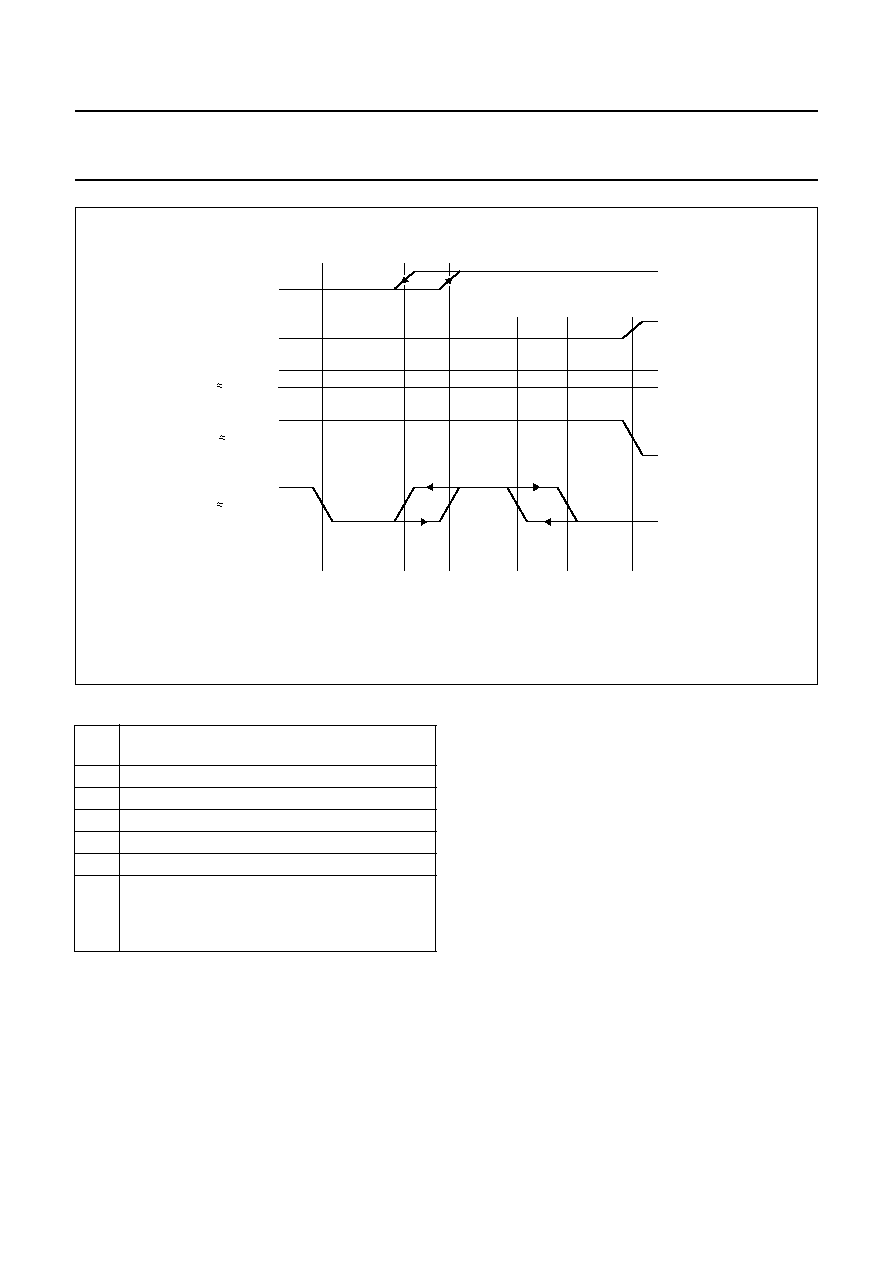
Fig.3 Operation of the three phase detector circuits.
MGA792
mute
(pin 13)
gating
1 detector
voltage
(pin 18)
I8 0.35 mA
1 detector
not gated
I8 1.0 mA
2 detector
not gated
I8 0.65 mA
3 detector
A
B
C
D
E
F
G
1
0
1
0
1
0
1
0
1
0
0.1 V
1.2 V
1.8 V
3.5 V
5 V
7.8 V
Explanation of areas A to G shown in Fig.3
A
switching over to new TV station activates 3 field
period counter
B
noise only condition
C
TV transmitter identification hysteresis range
D
fast time constant
C-E
fast time constant hysteresis range
F
normal time constant
G
sync pulse noise level detection circuit forces
pin 18 to
>
7.8 V while signal-to-noise level
<
19 dB; slow time constant and gated sync pulse
operation.
Supply (pins 9, 10 and 16)
The IC has been designed such that the horizontal
oscillator and output stage operate a very low supply
current into pin 16. The horizontal oscillator starts at a
supply current of approximately 4 mA (V
16
approximately
6 V). The horizontal output stage is forced into the
non-conducting stage until the supply current has reached
a typical value of 5 mA.
The circuit has been designed such that after starting the
horizontal output function, a current drop of approximately
1 mA is allowed.
The starting circuit has the ability to derive the main supply
(pin 10) from the horizontal output stage. The horizontal
output signal can also be used as oscillator signal for
synchronized switched-mode power supplies.

January 1994
10
Philips Semiconductors
Preliminary specification
Synchronization circuit with synchronized
vertical divider system for 60 Hz
TDA2579C
The maximum allowed starting current is 9.7 mA
(T
amb
= 25
∞
C).
The main supply should be connected to pin 10 and pin 9
should be used for ground. When the voltage on pin 10
increases from zero to its final value (typ. 12 V) a part of
the supply current of the starting circuit is taken from pin 10
via internal diodes and the voltage on pin 16 will stabilize
on a typical value of 9.3 V. In stabilized conditions
(V
10
>
10 V) the minimum required supply current into
pin 16 is approximately 2.5 mA.
All other IC functions are switched on via the main supply
voltage on pin 10. When this voltage reaches a value of
approximately 7 V the horizontal phase detector is
activated and the vertical ramp on pin 3 is started. The
second phase detector circuit and burst pulse circuit are
started when the voltage on pin 10 reaches the stabilized
voltage value of pin 16 typical 9.3 V.
To close the second phase detector loop a flyback pulse
must be applied to pin 12. When no flyback pulse is
detected the duty factor of the horizontal output stage
is 50%.
For remote switch-off pin 16 can be connected to ground
(via a npn transistor with a collector series resistor of
approximately 500
) which decreases pin 16 voltage to
5 V and switches off the horizontal output pulse.
Horizontal oscillator, horizontal output transistor and
second phase detector
The horizontal oscillator is connected to pin 15. The
frequency is set by an external RC combination between
pin 15 and ground (pin 9). The open collector horizontal
output stage is connected to pin 11. An internal Zener
diode configuration limits the open voltage of pin 11 to
approximately 14.5 V. The horizontal output transistor at
pin 11 is blocked until the current into pin 16 reaches a
value of approximately 5 mA.
A higher current results in a horizontal output signal at
pin 11, which starts with a duty factor of approximately
40% HIGH.
The duty factor is set by an internal current-source-loaded
npn emitter follower stage connected to pin 14 during
starting. When pin 16 changes over to voltage stabilization
the npn emitter follower and current source load at pin 14
are switched off and the second phase detector is
activated, provided a horizontal flyback pulse is present at
pin 12. When no flyback pulse is detected at pin 12 the
duty factor of the horizontal output stage is set to 50%. The
phase detector circuit at pin 14 compensates for storage
time in the horizontal deflection output state.
The horizontal output pulse duration is 29
µ
s HIGH for
storage times between 1
µ
s and 17
µ
s (flyback pulse of
12 to 29
µ
s). A higher storage time increases the
HIGH time.
Horizontal picture shift is possible by forcing an external
charge or discharge current into the capacitor at pin 14.
Mute output and 60 Hz identification (pin 13)
The collector of an npn transistor is connected to pin 13.
When the voltage on pin 18 drops below 1.2 V (no TV
transmitter) the npn transistor is switched on. When the
voltage on pin 18 increases to a level of approximately
1.8 V (new TV transmitter found) the npn transistor is
switched off.
This function is available when pin 13 is connected to
pin 10 (+12 V) via an external pull-up resistor of 10 to
20 k
. When no TV transmitter is identified the voltage on
pin 13 will be LOW (
<
0.5 V).
When an M-system TV transmitter with a divider ratio
<
576
(60 Hz) is found an internal pnp transistor with its emitter
connected to pin 13 will force the output voltage down to
approximately 7.6 V.
Sandcastle output (pin 17)
The sandcastle output pulse generated at pin 17 has three
different voltage levels. The highest level (10.4 V) can be
used for burst gating and black level clamping. The second
level (4.5 V) is obtained from the horizontal flyback pulse
at pin 12 and is used for horizontal blanking. The third level
(2.5 V) is used for vertical blanking and is derived via the
vertical divider system. For 60 Hz the blanking pulse
duration is 34 clock pulses started from the reset of the
vertical divider system.
For TV signals which have a divider ratio between 522 and
528 the vertical blanking pulse is started at the first
equalizing pulse.
January 1994
11
Philips Semiconductors
Preliminary specification
Synchronization circuit with synchronized
vertical divider system for 60 Hz
TDA2579C
LIMITING VALUES
In accordance with Absolute Maximum Rating System (IEC 134).
THERMAL RESISTANCE
CHARACTERISTICS
V
P
= V
10
= 12 V; I
16
= 6.2 mA; T
amb
= 25
∞
C; unless otherwise specified.
SYMBOL
PARAMETER
CONDITIONS
MIN.
MAX.
UNIT
I
16
start current
V
10
= 0 V
-
9.7
mA
V
P
supply voltage
-
13.2
V
P
tot
total power dissipation
-
1.2
W
T
stg
storage temperature
-
55
+150
∞
C
T
amb
operating ambient temperature
-
25
+70
∞
C
SYMBOL
PARAMETER
THERMAL RESISTANCE
R
th j-a
from junction to ambient in free air
50 K/W
SYMBOL
PARAMETER
CONDITIONS
MIN.
TYP.
MAX.
UNIT
Supply
V
P
supply voltage (pin 10)
10
12
13.2
V
I
16
supply current (pin 16)
note 1
V
10
= 0 V
6.2
-
9.7
mA
V
10
=
1 to 10 V;
T
amb
70
∞
C
6.2
-
8.7
mA
V
10
>
10 V
2.5
-
9.7
mA
V
16
stabilized voltage (pin 16)
8.8
9.3
9.7
V
I
10
current consumption (pin 10)
-
70
85
mA
Video input (pin 5)
V
5
top sync level
1.5
3.1
3.75
V
V
5(p-p)
sync pulse amplitude (peak-to-peak value)
note 2
0.05
0.6
1
V
SL
slicing level
note 3
35
50
65
%
t
d
delay between video input and detector
output
see Fig.5
0.2
0.3
0.55
µ
s
S/N
signal-to-noise ratio with sync pulse noise
level detector circuit active
CVBS = 1 V without
filter at pin 5; note 4
-
19
-
dB
Sync pulse
HYS
noise level detector circuit hysteresis
-
3
-
dB
Noise gate (pin 5)
V
5
switching level
-
0.7
1
V

January 1994
12
Philips Semiconductors
Preliminary specification
Synchronization circuit with synchronized
vertical divider system for 60 Hz
TDA2579C
First control loop (pin 8) horizontal oscillator to synchronization signal
f
holding range
±
700
±
800
-
Hz
f
catching range
±
700
±
800
±
1100
Hz
CS
control sensitivity video with respect to burst
key and flyback pulse:
slow time constant
note 5
-
2
-
kHz/
µ
s
normal time constant
note 6
-
5
-
kHz/
µ
s
fast time constant
note 6
-
3
-
kHz/
µ
s
10
phase modulation due to hum on the supply
line (peak-to-peak value)
note 7
-
0.2
-
µ
s/V
16
phase modulation due to hum on the input
current (peak-to-peak value)
note 8
-
0.08
-
µ
s/V
Second control loop (pin 14) horizontal flyback to horizontal oscillator
t
d
/
t
o
control sensitivity
t
d
= 10
µ
s
200
300
600
µ
s/
µ
s
t
d
control range
1
-
45
µ
s
t
d
control range for constant duty factor
horizontal output
1
29
-
t
FB
-
µ
s
control edge of horizontal output signal
(pin 11)
-
positive
-
Phase adjustment (pin 14) via second control loop
CS
control sensitivity
t
d
= 10
µ
s
-
25
-
µ
A/
µ
s
I
14
maximum allowed control current
-
-
±
60
µ
A
Horizontal oscillator (pin 15) C
osc
= 2.7 nF; R
osc
= 34.2 k
f
H
frequency (no sync)
-
15 625
-
Hz
f
H
spread (fixed external components,
no sync)
-
-
±
4
%
f
H
frequency deviation between starting point
output signal and stabilized condition
-
+5
+8
%
TC
temperature coefficient
-
-
1.10
-4
-
K
Horizontal output (pin 11) open collector
V
11H
HIGH level output voltage
-
-
13.2
V
V
11
start voltage protection
(internal Zener diode)
13
-
15.8
V
I
16L
LOW level input current protection output
enabled
-
5.0
6.2
mA
V
11L
LOW level output voltage start condition
I
11
= 10 mA
-
0.1
0.5
V
duty factor output current during starting
I
16
= 6.2 mA
50
60
70
%
V
11L
LOW level output voltage normal condition
I
11
= 25 mA
-
0.3
0.5
V
duty factor output current without flyback
pulse pin 12
45
50
55
%
SYMBOL
PARAMETER
CONDITIONS
MIN.
TYP.
MAX.
UNIT

January 1994
13
Philips Semiconductors
Preliminary specification
Synchronization circuit with synchronized
vertical divider system for 60 Hz
TDA2579C
t
OH
duration of output pulse HIGH
storage time
horizontal deflection
stage = 10
µ
s
27
29
31
µ
s
TC
temperature coefficient
-
-
4.10
-2
-
K
H
W
/H
d
influence of delay time on pulse width of
horizontal output signal
-
0.16
-
µ
s/
µ
s
controlled edge
-
positive
-
Sandcastle output signal (pin 17)
V
17
output voltage during:
burst key
9.8
10.4
-
V
horizontal blanking
I
load
= 1 mA
4.1
4.5
4.9
V
vertical blanking
I
load
= 0.3 mA
2.1
2.5
2.9
V
V
17
zero level output voltage
I
sink
= 0.5 mA
-
0.7
-
V
t
P
burst key pulse width
60 Hz
3.4
3.65
4
µ
s
V
12
horizontal blanking level
-
1
-
V
vertical blanking
note 9
t
d1
phase position burst key time between
middle sync pulse at pin 5 and start burst
key pulse at pin 17
2.3
2.7
3.1
µ
s
t
d2
phase position burst key time between start
sync pulse at pin 5 and end of burst key
pulse at pin 17
60 Hz
-
-
9.1
µ
s
Coincidence detector, video transmitter identification circuit and time constant switching levels (see Fig.1)
I
18
detector output current
-
0.25
-
mA
V
18
voltage level for in sync condition
1
normal
5.8
6.4
7
V
V
18
voltage level for noisy sync pulse
1
slow and gated
9
10.1
-
V
V
18
voltage level for noise only
note 10
-
0.3
-
V
V
18
switching level:
normal to fast
<
3.2
3.5
3.8
V
mute output active and fast to normal
<
1.0
1.2
1.4
V
field period counter
3 periods fast
<
0.08
0.12
0.16
V
normal to fast mute output inactive
locking
>
1.5
1.75
2
V
fast to normal
locking
>
4.7
5
5.3
V
normal to slow
gated sync pulse
>
7.4
7.8
8.2
V
Video transmitter identification output (pin 13)
V
13
output voltage active
no sync; I
13
= 2 mA
-
0.15
0.32
V
I
13
sink current active
no sync; V
13
= 1 V
-
-
5
mA
I
13
output current inactive
sync 60 Hz
-
-
1
µ
A
60 Hz identification (pin 13) R
13
positive supply 15 k
V
13
pnp emitter follower voltage
note 11
7.2
7.65
8.1
V
SYMBOL
PARAMETER
CONDITIONS
MIN.
TYP.
MAX.
UNIT

January 1994
14
Philips Semiconductors
Preliminary specification
Synchronization circuit with synchronized
vertical divider system for 60 Hz
TDA2579C
Flyback input pulse (pin 12)
V
12
switching voltage level
-
0.9
-
V
I
12
input current
0.2
-
3
mA
V
12(p-p)
input pulse (peak-to-peak value)
-
-
12
V
R
12
input resistance
-
3.5
-
k
t
d
phase position without shift; time between
the middle of the sync pulse at pin 5 and the
middle of the horizontal blanking pulse at
pin 17
2.1
2.5
2.9
µ
s
Vertical ramp generator (pin 3)
t
c
charge current pulse width
-
26t
clk
-
I
3
charge current
-
3
-
mA
V
3
top level ramp signal voltage divider in
60 Hz mode
note 12
4.55
4.85
5.25
V
V
3(p-p)
ramp amplitude (peak-to-peak value);
R
4
= 330 k
; f
V
= 60 Hz
C
3
= 150 nF; note 12
-
2.5
-
V
Current source (pin 4)
V
4
output voltage
I
4
= 20
µ
A
7
7.5
7.9
V
I
4
allowed current range
T
amb
= 25 to 70
∞
C
10
-
75
µ
A
TC
temperature coefficient output voltage
I
4
= 40
µ
A
-
50
-
10
-6
/K
Current source (pin 3)
I
3/4
current ratio pin 3/pin 4
I
4
= 35
µ
A; V
3
= 2 V
-
1.05
-
TC
temperature coefficient I
3
I
4
= 40
µ
A; R
4
fixed
-
100
-
10
-6
/K
Comparator (pin 2)
V
2
input voltage DC level
R
4
= 330 k
;
C
3
= 150 nF
0.98
1.075
1.17
V
V
2(p-p)
input voltage AC level (peak-to-peak value)
R
4
= 330 k
;
C
3
= 150 nF
-
0.8
-
V
I
2
input current
V
2
= 0 V
-
-
1
µ
A
Vertical output stage (pin 1) npn emitter follower
V
1
maximum output voltage
I
1
= +1.5 mA; note 12
5
5.5
6.3
V
R
S
sync separator resistor
-
170
-
I
sink
continuous sink current
-
0.25
-
mA
Vertical guard circuit (pin 2)
V
2H
active switching level HIGH
V
17
= 2.5 V; note 12
>
1.7
1.85
2.0
V
V
2L
active switching level LOW
V
17
= 2.5 V; note 12
<
0.25
0.35
0.45
V
SYMBOL
PARAMETER
CONDITIONS
MIN.
TYP.
MAX.
UNIT

January 1994
15
Philips Semiconductors
Preliminary specification
Synchronization circuit with synchronized
vertical divider system for 60 Hz
TDA2579C
Notes to the characteristics
1. Value inclusive R
L
pin 11 to pin 16 = 6.8 k
.
2. Up to 1 V peak-to-peak the slicing level is constant, at amplitudes exceeding 1 V peak-to-peak the slicing level will
increase.
3. The slicing level is fixed by the formula:
Where R
S
is the resistor between pins 6 and in k
; top sync = 100%.
4. S/N
A low-pass filter of 1 k
and 150 pF decreases the noise content of the CVBS signal by 6 dB.
5. Undercompensated.
6. Overcompensated.
7. Measured between pin 5 and sandcastle output pin 17.
8. Measured with 3.3
µ
F feedback capacitor between pin 16 and 6.8
µ
F capacitor in PLL filter pin 8.
9. Maximum divider ratio (60 Hz):
Start vertical blanking:
-
search (large) window mode (60 Hz)
-
reset divider = start vertical sync pulse plus 1 clock pulse
-
small/standard window mode (60 Hz)
-
clock pulse 517.
Stop vertical blanking:
-
all window modes (60 Hz)
-
clock pulse 34.
10. Depends on DC level of pin 5, value given is valid for V
5
5 V.
11. Valid for
12. Value related to internal Zener diode reference voltage. Spread includes complete spread of reference voltage.
Internal vertical sync pulse separator
t
d1
delay between video signal at pin 5 and
internally separated vertical sync pulse;
normal signal condition
12
19
25
µ
s
t
d2
delay between video signal at pin 5 and
internally separated vertical sync pulse;
noisy signal condition
V
18
1.2 V
-
-
-
17
µ
s
SYMBOL
PARAMETER
CONDITIONS
MIN.
TYP.
MAX.
UNIT
p
R
s
5.3
R
s
◊
---------------------
100%.
◊
=
= 20 log
Video voltage (black-to-white signal)
Noise (RMS)
------------------------------------------------------------------------------------------------
n
2
f
H
◊
f
V
--------------
576 (2 clock pulses per video line).
=
=
2
f
H
◊
f
V
--------------
576.
<

January 1994
16
Philips Semiconductors
Preliminary specification
Synchronization circuit with synchronized
vertical divider system for 60 Hz
TDA2579C
Fig.4 Counter system.
10
26
34
130
160
488
525
517
528
576
0
start
vertical sawtooth charge pulse
blocking pulse phase detector 1
vertical blanking
search mode
end of blocking pulse (60 Hz)
end of vertical sawtooth charge pulse
end of vertical blanking (60 Hz)
noise detector window
start
blocking pulse phase detector 1 (60 Hz)
vertical blanking (60 Hz)
normal and narrow window
normal reset
reset divider when mute is active; no vertical sync found
60 Hz
identification
search
window
MGA793
One video line equals two counter pulses.
Reset counter 32
µ
s after start of vertical sync pulse at pin 5.
Reset counter = counter state 0.

January 1994
17
Philips Semiconductors
Preliminary specification
Synchronization circuit with synchronized
vertical divider system for 60 Hz
TDA2579C
Fig.5 Timing diagram.
Two counter pulses equals one video line.
MGA794
10.4 V
4.5 V
1/2 t FB
storage time
horizontal
deflection stage
switching level
video input
separated
horizontal
sync pulse
horizontal
oscillator
sawtooth
internal
gating
pulse
0V
2.5 V
reference
detector
1
output I8
detector
1
reference level
1
2
reference level
0.3 s
µ
4.7 s
µ
5-9
signal V
horizontal
flyback
pulse
2.5 s
µ
7.5 s
µ
3.75 s
µ
3.75 s
µ
coincidence
detector
18
output I
reference
detector
2
external
horizontal
flyback
pulse V12-9
output I14
detector
2
29 s
µ
horizontal
output
signal V11-9
sandcastle
output
signal V17-9
0.2 s
µ
t P
12 s
µ
6 s
µ
0.7 V
divider in search window mode
60 Hz: 34 clock pulses
other divider modes
60 Hz: 42 clock pulses
1/2 t FB
t FB

January 1994
18
Philips Semiconductors
Preliminary specification
Synchronization circuit with synchronized
vertical divider system for 60 Hz
TDA2579C
MGA796
560
880
C
8.4
k
560
880
C
4.7
k
560
880
C
2.4
k
2.4
k
9.5
k
4
k
D
18
k
36 k
V
2.8 V
ref
DETECTOR
1
C
A
B
9
k
360
5.6
k
A
6.2
k
A
4.3
k
SYNC SEPARATOR
2 V reference
0 V
1 k
150 pF
2 k
10 k
A
11
k
10.5
k
1
k
6
k
B
2
k
3.5
k
noise
detector
5
VIDEO
INPUT
7.7
k
1.5 k
1.3
k
1.5 k
200
I
V
stab
VERTICAL SAWTOOTH GENERATOR
2.15
k
2 k
I
K
160
150
2
k
µ
A
250
µ
A
250
5.1 k
1 k
12 k
1.2
k
12
k
60 Hz
identification
6
k
11
k
2.7
k
1.8 k
1.4 mA
160
0.8 mA
1.4 mA
1 k
2
detector
stabilizer
5.6
k
11
k
G
H
pin 16
pin 10
G
start up
3.9 k
2.2 k
2.2 k
2
I
H
G
II
I
pin 16
start up
E
F
pin 10
E
F
D
220
stabilizer
6.2
k
DETECTOR
2
HORIZONTAL OSCILLATOR
HORIZONTAL
FLYBACK
HORIZONTAL OUTPUT
VERTICAL COMPARATOR
V
stabilizer
VERTICAL DRIVER
COINCIDENCE DETECTOR
TRANSMITTER IDENTIFICATION
SANDCASTLE
SUPPLY
12 V
6.8
k
pin 16
3.0 mA
0.2 mA
100 nF
33 k
4.7 k
2.7 nF
1.2 k
68 nF
µ
F
6.8
22
µ
F
22
µ
F
2.2
5.6
k
µ
F
4.7
3.6
k
43
k
150 nF
150
k
220
k
4.3
k
4.3
k
100 nF
15
k
12 V
TDA2579C
4
3
2
1
18
13
17
9
16
10
11
12
14
15
8
7
6
K
Fig.6 Internal circuitry

January 1994
19
Philips Semiconductors
Preliminary specification
Synchronization circuit with synchronized
vertical divider system for 60 Hz
TDA2579C
Fig.7 TDA2579C and TDA3654 combination 110
∞
Flat Square picture tube.
(1) Dependent on printed-circuit board layout.
MGA795
9
100 nF
12
10
16
15
8
5
13
14
7
6
11
4.7
nF
sandcastle
horizontal
drive
horizontal
flyback
150 nF
4
3
2
1
17
22
µ
F
68 nF
6.8
µ
F
1.2 k
video
input
22
µ
F
22
5.6 k
100
nF
12 V
26 V
18
2.2
µ
F
150
pF
220
k
150
k
k
1
0.5
3.6 k
4.7
µ
F
TDA2579C
47
k
6.8 k
100
µ
F
12 k
39 k
0.2 to
3.0 mA
horizontal
shift
2.7
nF
100
k
33
k
4.7
k
f adj.
o
start
voltage
6.2 mA to 9.7 mA
transmission
identification
60 Hz
identification
10
nF
1 k
1 k
43 k
1000
µ
F
DEFLECTION
COIL
270
4.3 k
4.3 k
470 pF
(1)
220
µ
F
560
4.7
100
µ
F
BAX12
VERTICAL DEFLECTION CIRCUIT
TDA3654
9
8
5
7
6
4
3
2
1
1 nF
10 nF
(1)
January 1994
20
Philips Semiconductors
Preliminary specification
Synchronization circuit with synchronized
vertical divider system for 60 Hz
TDA2579C
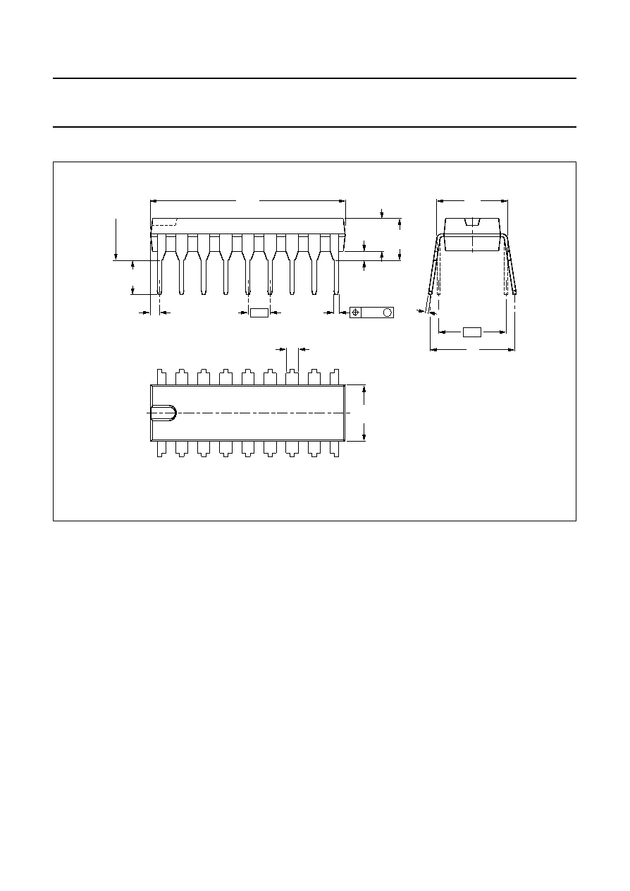
PACKAGE OUTLINE
Fig.8 18-lead dual in-line; plastic (SOT102).
Dimensions in mm.
8.25
7.80
0.32 max
7.62
9.5
8.3
MSA259
18
1
10
9
1.4 max
6.48
6.14
22.00
21.35
3.7
max 4.7
max
0.51
min
3.9
3.4
seating plane
0.254
M
0.53
max
2.54
(8x)
0.85
max
SOLDERING
Plastic dual in-line packages
B
Y DIP OR WAVE
The maximum permissible temperature of the solder is
260
∞
C; this temperature must not be in contact with the
joint for more than 5 s. The total contact time of successive
solder waves must not exceed 5 s.
The device may be mounted up to the seating plane, but
the temperature of the plastic body must not exceed the
specified storage maximum. If the printed-circuit board has
been pre-heated, forced cooling may be necessary
immediately after soldering to keep the temperature within
the permissible limit.
R
EPAIRING SOLDERED JOINTS
Apply the soldering iron below the seating plane (or not
more than 2 mm above it). If its temperature is below
300
∞
C, it must not be in contact for more than 10 s; if
between 300 and 400
∞
C, for not more than 5 s.

January 1994
21
Philips Semiconductors
Preliminary specification
Synchronization circuit with synchronized
vertical divider system for 60 Hz
TDA2579C
DEFINITIONS
LIFE SUPPORT APPLICATIONS
These products are not designed for use in life support appliances, devices, or systems where malfunction of these
products can reasonably be expected to result in personal injury. Philips customers using or selling these products for
use in such applications do so at their own risk and agree to fully indemnify Philips for any damages resulting from such
improper use or sale.
Data sheet status
Objective specification
This data sheet contains target or goal specifications for product development.
Preliminary specification
This data sheet contains preliminary data; supplementary data may be published later.
Product specification
This data sheet contains final product specifications.
Limiting values
Limiting values given are in accordance with the Absolute Maximum Rating System (IEC 134). Stress above one or
more of the limiting values may cause permanent damage to the device. These are stress ratings only and operation
of the device at these or at any other conditions above those given in the Characteristics sections of the specification
is not implied. Exposure to limiting values for extended periods may affect device reliability.
Application information
Where application information is given, it is advisory and does not form part of the specification.

January 1994
22
Philips Semiconductors
Preliminary specification
Synchronization circuit with synchronized
vertical divider system for 60 Hz
TDA2579C
NOTES

January 1994
23
Philips Semiconductors
Preliminary specification
Synchronization circuit with synchronized
vertical divider system for 60 Hz
TDA2579C
NOTES

Philips Semiconductors
Philips Semiconductors ≠ a worldwide company
Argentina: IEROD, Av. Juramento 1992 - 14.b, (1428)
BUENOS AIRES, Tel. (541)786 7633, Fax. (541)786 9367
Australia: 34 Waterloo Road, NORTH RYDE, NSW 2113,
Tel. (02)805 4455, Fax. (02)805 4466
Austria: Triester Str. 64, A-1101 WIEN, P.O. Box 213,
Tel. (01)60 101-1236, Fax. (01)60 101-1211
Belgium: Postbus 90050, 5600 PB EINDHOVEN, The Netherlands,
Tel. (31)40 783 749, Fax. (31)40 788 399
Brazil: Rua do Rocio 220 - 5
th
floor, Suite 51,
CEP: 04552-903-S√O PAULO-SP, Brazil.
P.O. Box 7383 (01064-970).
Tel. (011)829-1166, Fax. (011)829-1849
Canada: INTEGRATED CIRCUITS:
Tel. (800)234-7381, Fax. (708)296-8556
DISCRETE SEMICONDUCTORS: 601 Milner Ave,
SCARBOROUGH, ONTARIO, M1B 1M8,
Tel. (0416)292 5161 ext. 2336, Fax. (0416)292 4477
Chile: Av. Santa Maria 0760, SANTIAGO,
Tel. (02)773 816, Fax. (02)777 6730
Colombia: Carrera 21 No. 56-17, BOGOTA, D.E., P.O. Box 77621,
Tel. (571)217 4609, Fax. (01)217 4549
Denmark: Prags Boulevard 80, PB 1919, DK-2300 COPENHAGEN S,
Tel. (032)88 2636, Fax. (031)57 1949
Finland: Sinikalliontie 3, FIN-02630 ESPOO,
Tel. (9)0-50261, Fax. (9)0-520971
France: 4 rue du Port-aux-Vins, BP317,
92156 SURESNES Cedex,
Tel. (01)4099 6161, Fax. (01)4099 6427
Germany: P.O. Box 10 63 23, 20095 HAMBURG ,
Tel. (040)3296-0, Fax. (040)3296 213
Greece: No. 15, 25th March Street, GR 17778 TAVROS,
Tel. (01)4894 339/4894 911, Fax. (01)4814 240
Hong Kong: 15/F Philips Ind. Bldg., 24-28 Kung Yip St.,
KWAI CHUNG, Tel. (0)4245 121, Fax. (0)4806 960
India: PEICO ELECTRONICS & ELECTRICALS Ltd.,
Components Dept., Shivsagar Estate, Block 'A',
Dr. Annie Besant Rd., Worli, BOMBAY 400 018,
Tel. (022)4938 541, Fax. (022)4938 722
Indonesia: Philips House, Jalan H.R. Rasuna Said Kav. 3-4,
P.O. Box 4252, JAKARTA 12950,
Tel. (021)5201 122, Fax. (021)5205 189
Ireland: Newstead, Clonskeagh, DUBLIN 14,
Tel. (01)640 000, Fax. (01)640 200
Italy: Viale F. Testi, 327, 20162 MILANO,
Tel. (02)6752.1, Fax. (02)6752.3350
Japan: Philips Bldg 13-37, Kohnan 2 -chome, Minato-ku, KOKIO 108,
Tel. (03)3740 5101, Fax. (03)3740 0570
Korea: (Republic of) Philips House, 260-199 Itaewon-dong,
Yongsan-ku, SEOUL, Tel. (02)794-5011, Fax. (02)798-8022
Malaysia: No. 76 Jalan Universiti, 46200 PETALING JAYA,
SELANGOR, Tel. (03)757 5511, Fax. (03)757 4880
Mexico: Philips Components, 5900 Gateway East, Suite 200,
EL PASO, TX 79905, Tel. 9-5(800)234-7381, Fax. (708)296-8556
Netherlands: Postbus 90050, 5600 PB EINDHOVEN,
Tel. (040)78 37 49, Fax. (040)78 83 99
New Zealand: 2 Wagener Place, C.P.O. Box 1041, AUCKLAND,
Tel. (09)849-4160, Fax. (09)849-7811
Norway: Box 1, Manglerud 0612, OSLO,
Tel. (22)74 8000, Fax. (22)74 8341
Pakistan: Philips Markaz, M.A. Jinnah Rd., KARACHI 3,
Tel. (021)577 039, Fax. (021)569 1832
Philippines: PHILIPS SEMICONDUCTORS PHILIPPINES Inc,
106 Valero St. Salcedo Village, P.O. Box 911, MAKATI,
Metro MANILA, Tel. (02)810 0161, Fax. (02)817 3474
Portugal: Av. Eng. Duarte Pacheco 6, 1009 LISBOA Codex,
Tel. (01)683 121, Fax. (01)658 013
Singapore: Lorong 1, Toa Payoh, SINGAPORE 1231,
Tel. (65)350 2000, Fax. (65)251 6500
South Africa: 195-215 Main Road, Martindale,
P.O. Box 7430,JOHANNESBURG 2000,
Tel. (011)470-5433, Fax. (011)470-5494
Spain: Balmes 22, 08007 BARCELONA,
Tel. (03)301 6312, Fax. (03)301 42 43
Sweden: Kottbygatan 7, Akalla. S-164 85 STOCKHOLM,
Tel. (0)8-632 2000, Fax. (0)8-632 2745
Switzerland: Allmendstrasse 140, CH-8027 ZÐRICH,
Tel. (01)488 2211, Fax. (01)481 7730
Taiwan: 69, Min Sheng East Road, Sec 3, P.O. Box 22978,
TAIPEI 10446, Tel. (2)509 7666, Fax. (2)500 5899
Thailand: PHILIPS ELECTRONICS (THAILAND) Ltd.,
60/14 MOO 11, Bangna - Trad Road Km. 3
Prakanong, BANGKOK 10260,
Tel. (2)399-3280 to 9, (2)398-2083, Fax. (2)398-2080
Turkey: Talatpasa Cad. No. 5, 80640 LEVENT/ISTANBUL,
Tel. (0212)279 2770, Fax. (0212)269 3094
United Kingdom: Philips Semiconductors Limited, P.O. Box 65,
Philips House, Torrington Place, LONDON, WC1E 7HD,
Tel. (071)436 41 44, Fax. (071)323 03 42
United States: INTEGRATED CIRCUITS:
811 East Arques Avenue, SUNNYVALE, CA 94088-3409,
Tel. (800)234-7381, Fax. (708)296-8556
DISCRETE SEMICONDUCTORS: 2001 West Blue Heron Blvd.,
P.O. Box 10330, RIVIERA BEACH, FLORIDA 33404,
Tel. (800)447-3762 and (407)881-3200, Fax. (407)881-3300
Uruguay: Coronel Mora 433, MONTEVIDEO,
Tel. (02)70-4044, Fax. (02)92 0601
For all other countries apply to: Philips Semiconductors,
International Marketing and Sales, Building BAF-1,
P.O. Box 218, 5600 MD, EINDHOVEN, The Netherlands,
Telex 35000 phtcnl, Fax. +31-40-724825
SCD27
© Philips Electronics N.V. 1993
All rights are reserved. Reproduction in whole or in part is prohibited without the
prior written consent of the copyright owner.
The information presented in this document does not form part of any quotation
or contract, is believed to be accurate and reliable and may be changed without
notice. No liability will be accepted by the publisher for any consequence of its
use. Publication thereof does not convey nor imply any license under patent- or
other industrial or intellectual property rights.
Printed in The Netherlands
9397 725 20011