 | –≠–ª–µ–∫—Ç—Ä–æ–Ω–Ω—ã–π –∫–æ–º–ø–æ–Ω–µ–Ω—Ç: TDA2595V9 | –°–∫–∞—á–∞—Ç—å:  PDF PDF  ZIP ZIP |
DATA SHEET
Product specification
File under Integrated Circuits, IC02
March 1987
INTEGRATED CIRCUITS
TDA2595
Horizontal combination

March 1987
2
Philips Semiconductors
Product specification
Horizontal combination
TDA2595
GENERAL DESCRIPTION
The TDA2595 is a monolithic integrated circuit intended for use in colour television receivers.
Features
∑
Positive video input; capacitively coupled (source impedance
<
200
)
∑
Adaptive sync separator; slicing level at 50% of sync amplitude
∑
Internal vertical pulse separator with double slope integrator
∑
Output stage for vertical sync pulse or composite sync depending on the load; both are switched off at muting
∑
1
phase control between horizontal sync and oscillator
∑
Coincidence detector
3
for automatic time-constant switching; overruled by the VCR switch
∑
Time-constant switch between two external time-constants or loop-gain; both controlled by the coincidence detector
3
∑
1
gating pulse controlled by coincidence detector
3
∑
Mute circuit depending on TV transmitter identification
∑
2
phase control between line flyback and oscillator; the slicing levels for
2
control and horizontal blanking can be set
separately
∑
Burst keying and horizontal blanking pulse generation, in combination with clamping of the vertical blanking pulse
(three-level sandcastle)
∑
Horizontal drive output with constant duty cycle inhibited by the protection circuit or the supply voltage sensor
∑
Detector for too low supply voltage
∑
Protection circuit for switching off the horizontal drive output continuously if the input voltage is below 4 V or higher
than 8 V
∑
Line flyback control causing the horizontal blanking level at the sandcastle output continuously in case of a missing
flyback pulse
∑
Spot-suppressor controlled by the line flyback control
QUICK REFERENCE DATA
PACKAGE OUTLINE
18-lead DIL; plastic (SOT102); SOT102-1; 1997 January 07.
Supply voltage (pin 15)
V
15-5
= V
P
typ.
12
V
Sync pulse amplitude (positive video)
V
i(p-p)
min.
50
mV
Horizontal output current
I
4
typ.
50
mA
March 1987
3
Philips Semiconductors
Product specification
Horizontal combination
TDA2595
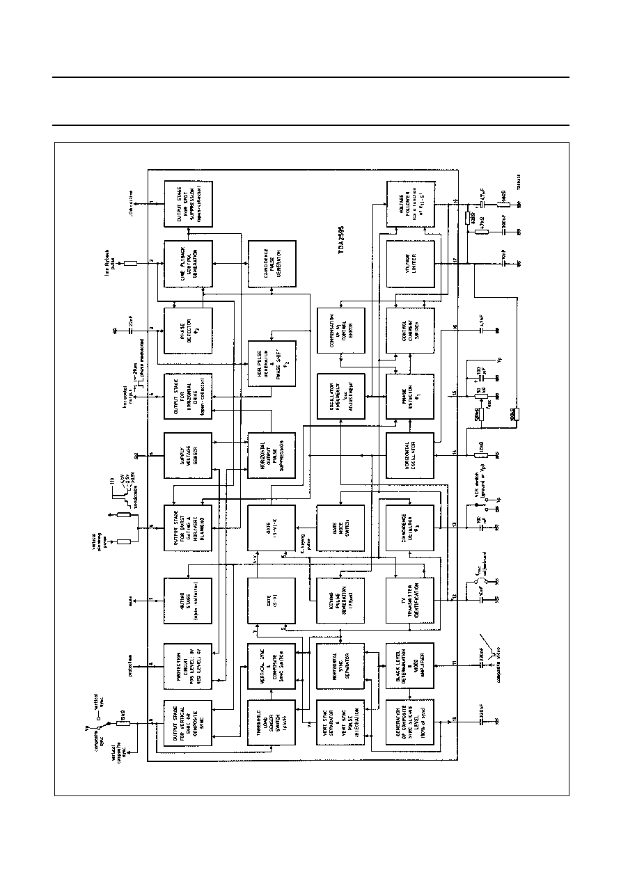
Fig.1 Block diagram.

March 1987
4
Philips Semiconductors
Product specification
Horizontal combination
TDA2595
RATINGS
Limiting values in accordance with the Absolute Maximum System (IEC 134)
Supply voltage (pin 15)
V
15-5
= V
P
max.
13,2
V
Voltages at:
pins 1, 4 and 7
V
1;4;7-5
max.
18
V
pins 8, 13 and 18
V
8;13;18-5
max.
V
P
V
pin 11 (range)
V
11-5
-
0,5 to
+
6
V
Currents at:
pin 1
I
1
max.
10
mA
pin 2 (peak value)
±
I
2M
max.
10
mA
pin 4
I
4
max.
100
mA
pin 6 (peak value)
±
I
6M
max.
6
mA
pin 7
I
7
max.
10
mA
pin 8 (range)
I
8
-
5 to
+
1
mA
pin 9 (range)
I
9
-
10 to
+
3
mA
pin 18
±
I
18
max.
10
mA
Total power dissipation
P
tot
max.
800
mW
Storage temperature range
T
stg
-
25 to
+
125
∞
C
Operating ambient temperature range
T
amb
0 to
+
70
∞
C

March 1987
5
Philips Semiconductors
Product specification
Horizontal combination
TDA2595
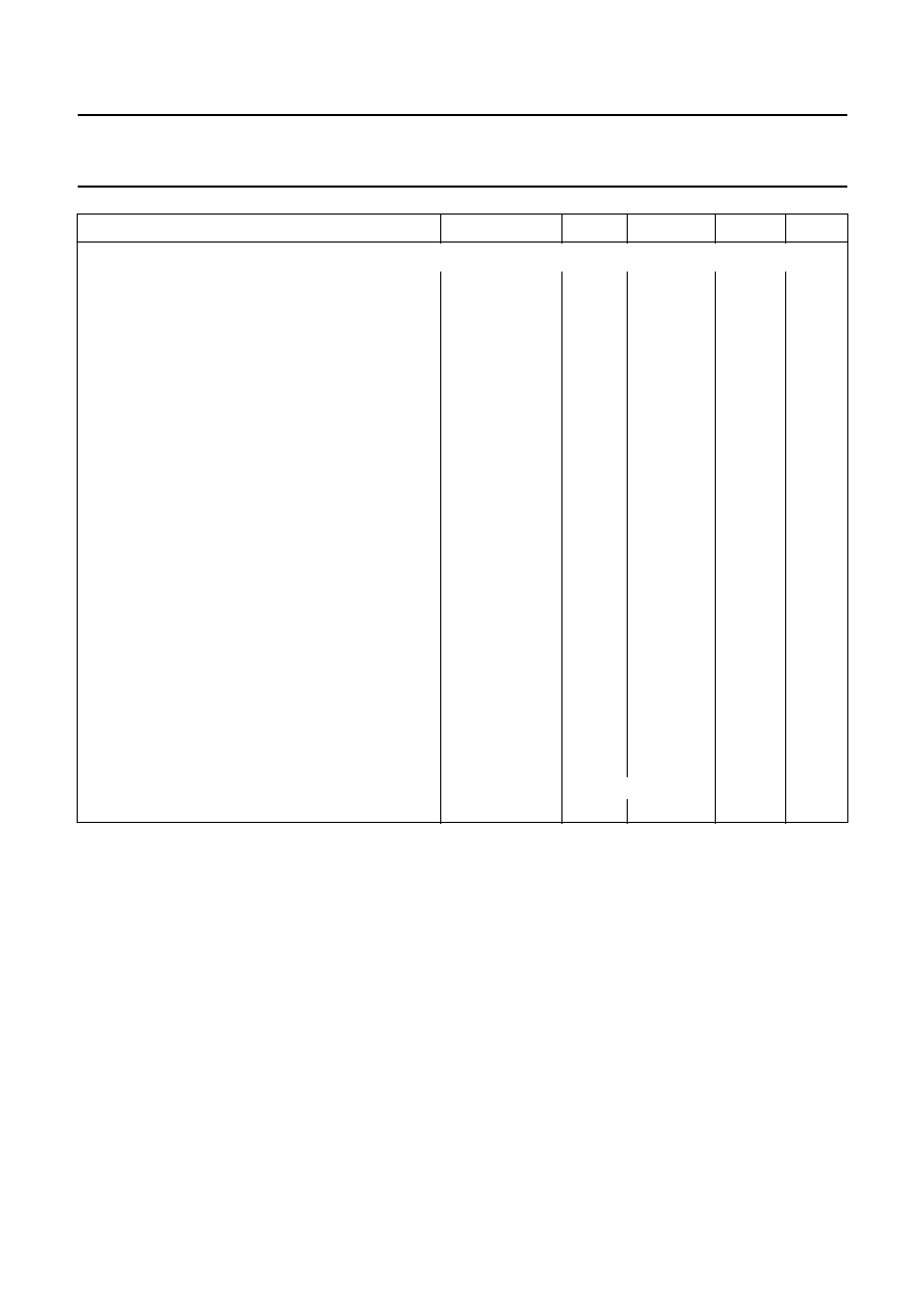
CHARACTERISTICS
V
P
= 12 V; T
amb
= 25
∞
C; measured in Fig.1; unless otherwise specified
PARAMETER
SYMBOL
MIN.
TYP.
MAX.
UNIT
Composite video input and sync separator (pin 11)
(internal black level determination)
Input signal (positive video;
standard signal; peak-to-peak value)
V
11-5(p-p)
0,2
1
3
V
Sync pulse amplitude
(independent of video content)
V
11-5(p-p)
50
-
-
mV
Generator resistance
R
G
-
-
200
Input current during:
video
I
11
-
5
-
µ
A
sync pulse
-
I
11
-
40
-
µ
A
black level
-
I
11
-
25
-
µ
A
Composite sync generation (pin 10)
horizontal slicing level at 50% of the sync pulse
amplitude for V
11-5(p-p)
<
1,5 V
Capacitor current during:
video
I
10
-
16
-
µ
A
sync pulse
-
I
10
-
170
-
µ
A
Vertical sync pulse generation
slicing level at 30% (60% between black level and
horizontal slicing level); pin 9
Output voltage
V
9-5
10
-
-
V
Pulse duration
t
p
-
190
-
µ
s
Delay with respect to the vertical
sync pulse (leading edge)
t
d
-
45
-
µ
s
Pulse-mode control
output current for vertical sync pulse (dual
integrated)
no current applied at
pin 9
output current for horizontal and vertical sync pulse
(non-integrated separated signal)
current applied via a
resistor of 15 k
from V
P
to pin 9

March 1987
6
Philips Semiconductors
Product specification
Horizontal combination
TDA2595
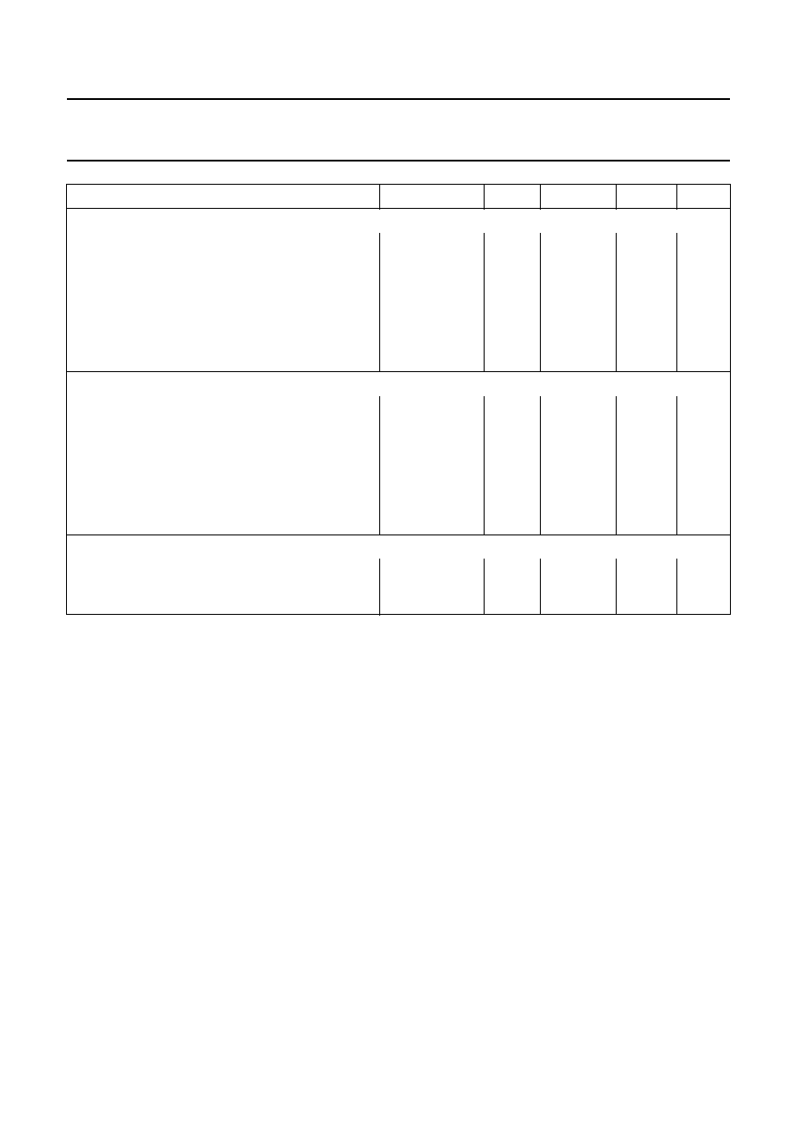
Horizontal oscillator
(pins 14 and 16)
Frequency; free running
f
osc
-
15 625
-
Hz
Reference voltage for f
osc
V
14-5
-
6
-
V
Frequency control sensitivity
f
osc
/
I
14
-
31
-
Hz/
µ
A
Adjustment range of circuit Fig.1
f
osc
-
±
10
-
%
Spread of frequency
f
osc
-
-
5
%
Frequency dependency (excluding
tolerance of external (components)
-
±
0,05
-
with supply voltage (V
P
= 12 V)
with supply voltage drop of 5 V
f
osc
-
-
10
%
with temperature
TC
-
-
±
10
-
4
K
-
1
Capacitor current during:
discharging
+
I
16
-
1024
-
µ
A
charging
-
I
16
-
313
-
µ
A
Sawtooth voltage timing (pin 14)
rise time
t
r
-
49
-
µ
s
fall time
t
f
-
15
-
µ
s
Horizontal output pulse (pin 4)
Output voltage LOW at I
4
= 50 mA
V
4-5
-
-
0,5
V
Pulse duration (HIGH)
t
p
-
29
±
1,5
-
µ
s
Supply voltage for switching off
the output pulse (pin 15)
V
P
-
4
-
V
Hysteresis for switching
on the output pulse
V
P
-
250
-
mV
PARAMETER
SYMBOL
MIN.
TYP.
MAX.
UNIT
f
osc
f
osc
/
V
15
5
≠
V
15
5
≠
/
----------------------------------------
March 1987
7
Philips Semiconductors
Product specification
Horizontal combination
TDA2595
Phase comparison
1
(pin 17)
Control voltage range
V
17-5
3,55
-
8,3
V
Leakage current
at V
17-5
= 3,55 to 8,3 V
I
17
-
-
1
µ
A
Control current for external
time-constant switch
±
I
17
1,8
2
2,2
mA
Control current at V
18-5
= V
15-5
and V
13-5
<
2 V or V
13-5
>
9,5 V
±
I
17
-
8
-
mA
Control current at V
18-5
= V
15-5
and V
13-5
= 2 to 9,5 V
±
I
17
1,8
2
2,2
mA
Horizontal oscillator control
control sensitivity
S
6
-
-
kHz/
µ
s
catching and holding range
±
f
osc
-
680
-
Hz
spread of catching and holding range
±
f
osc
-
10
-
%
Internal keying pulse
at V
13-5
= 2,9 to 9,5 V
t
p
-
7,5
-
µ
s
Time-constant switch
slow time-constant at
V
13-5
9,5
-
2
V
fast time-constant at
V
13-5
2
-
9,5
V
Impedance converter offset voltage
(slow time-constant)
±
V
17-18
-
-
3
mV
Output resistance
slow time-constant
R
18-5
-
-
10
fast time-constant
R
18-5
high impedance
Leakage current
I
18
-
-
1
µ
A
PARAMETER
SYMBOL
MIN.
TYP.
MAX.
UNIT

March 1987
8
Philips Semiconductors
Product specification
Horizontal combination
TDA2595
Coincidence detector
3
(pin 13)
Output voltage
without coincidence with composite video signal
V
13-5
-
-
1
V
without coincidence without composite video signal
(noise)
V
13-5
-
-
2
V
with coincidence with composite video signal
V
13-5
-
6
-
V
Output current
without coincidence with composite video signal
I
13
-
50
-
µ
A
with coincidence with composite video signal
-
I
13
-
300
-
µ
A
Switching current
at V
13-5
= V
P
-
0,5 V
I
13
-
-
100
µ
A
at V
13-5
= 0,5 V (average value)
I
13(av)
-
-
100
µ
A
Phase comparison
2
(pins 2 and 3) (see note 1)
Input for line flyback pulse (pin 2)
Switching level for
2
comparison
and flyback control
V
2-5
-
3
-
V
Switching level for horizontal blanking
V
2-5
-
0,3
-
V
Input voltage limiting
V
2-5
-
-
0,7
-
V
or:
-
+
4,5
-
V
Switching current
at horizontal flyback
I
2
0,01
1
-
mA
at horizontal scan
I
2
-
-
2
µ
A
Maximum negative input current
-
I
2
-
-
500
µ
A
Phase detector output (pin 3)
Control current for
2
±
I
3
-
1
-
mA
Control range
t
2
-
19
-
µ
s
Static control error
t /
t
d
-
-
0,2
%
Leakage current
I
3
-
-
5
µ
A
PARAMETER
SYMBOL
MIN.
TYP.
MAX.
UNIT

March 1987
9
Philips Semiconductors
Product specification
Horizontal combination
TDA2595
Phase comparison
2
(pins 2 and 3) (continued)
Phase relation between middle of the
horizontal sync pulse and the middle of the line
flyback pulse at t
fp
= 12
µ
s (note 2)
t
-
2,6
±
0,7
-
µ
s
If additional adjustment is
required, it can be arranged by applying a current at
pin 3
I/
t
-
30
-
µ
A/
µ
s
Burst gating pulse (pin 6) (note 3)
Output voltage
V
6-5
10
11
-
V
Pulse duration
t
p
3,7
4
4,3
µ
s
Phase relation between middle of
sync pulse at the input and the leading edge of the
burst gating pulse at V
6-5
= 7 V
t
6
2,15
2,65
3,15
µ
s
Output trailing edge current
I
6
-
2
-
mA
Horizontal blanking pulse (pin 6) (note 3)
Output voltage
V
6-5
4,1
4,5
4,9
V
Output trailing edge current
I
6
-
2
-
mA
Saturation voltage at horizontal scan
V
6-5sat
-
-
0,5
V
Clamping circuit for vertical blanking pulse (pin 6) (note 3)
Output voltage at I
6
= 2,8 mA
V
6-5
2,15
2,5
3
V
Minimum output current
at V
6-5
>
2,15 V
I
6min
-
2,3
-
mA
Maximum output current
at V
6-5
<
3 V
I
6max
-
3,3
-
mA
TV-transmitter identification (pin 12) (note 4)
Output voltage
no TV transmitter
V
12-5
-
-
1
V
TV transmitter identified
V
12-5
7
-
-
V
PARAMETER
SYMBOL
MIN.
TYP.
MAX.
UNIT
March 1987
10
Philips Semiconductors
Product specification
Horizontal combination
TDA2595
Notes to the characteristics
1. Phase comparison between horizontal oscillator and the line flyback pulse. Generation of a phase modulated
(
2
) horizontal output pulse with constant duration.
2. t
fp
is the line flyback pulse duration.
3. Three-level sandcastle pulse.
4. If pin 12 is connected to V
p
the vertical output is active independent of synchronization state.
Mute output (pin 7)
Output voltage at I
7
= 3 mA
no TV transmitter
V
7-5
-
-
0,5
V
Output resistance at I
7
= 3 mA
no TV transmitter
R
7-5
-
-
100
Output leakage current
at V
12-5
>
3 V
TV transmitter identified
I
7
-
-
5
µ
A
Protection circuit (beam-current/ EHT voltage protection) (pin 8)
No-load voltage for I
8
= 0
(operative condition)
V
8-5
-
6
-
V
Threshold at positive-going voltage
V
8-5
-
8
±
0,8
-
V
Threshold at negative-going voltage
V
8-5
-
4
±
0,4
-
V
Current limiting for V
8-5
= 1 to 8,5 V
±
I
8
-
60
-
µ
A
Input resistance for V
8-5
>
8,5 V
R
8-5
-
3
-
k
Internal response delay of threshold switch
t
d
-
10
-
µ
s
Control output of line flyback pulse control (pin 1)
Saturation voltage at standard operation; I
7
= 3 mA
V
1-5sat
-
-
0,5
V
Output leakage current in case of disturbance of line
flyback pulse
I
1
-
-
5
µ
A
PARAMETER
SYMBOL
MIN.
TYP.
MAX.
UNIT

March 1987
11
Philips Semiconductors
Product specification
Horizontal combination
TDA2595
PACKAGE OUTLINE
REFERENCES
OUTLINE
VERSION
EUROPEAN
PROJECTION
ISSUE DATE
IEC
JEDEC
EIAJ
SOT102-1
93-10-14
95-01-23
UNIT
A
max.
1
2
b
1
(1)
(1)
(1)
b
2
c
D
E
e
M
Z
H
L
mm
DIMENSIONS (inch dimensions are derived from the original mm dimensions)
A
min.
A
max.
b
max.
w
M
E
e
1
1.40
1.14
0.53
0.38
0.32
0.23
21.8
21.4
6.48
6.20
3.9
3.4
0.254
2.54
7.62
8.25
7.80
9.5
8.3
0.85
4.7
0.51
3.7
inches
0.055
0.044
0.021
0.015
0.013
0.009
1.40
1.14
0.055
0.044
0.86
0.84
0.26
0.24
0.15
0.13
0.01
0.10
0.30
0.32
0.31
0.37
0.33
0.033
0.19
0.020
0.15
M
H
c
(e )
1
M
E
A
L
seating plane
A
1
w
M
b
1
b
2
e
D
A
2
Z
18
1
10
9
b
E
pin 1 index
0
5
10 mm
scale
Note
1. Plastic or metal protrusions of 0.25 mm maximum per side are not included.
DIP18: plastic dual in-line package; 18 leads (300 mil)
SOT102-1

March 1987
12
Philips Semiconductors
Product specification
Horizontal combination
TDA2595
SOLDERING
Introduction
There is no soldering method that is ideal for all IC packages. Wave soldering is often preferred when through-hole and
surface mounted components are mixed on one printed-circuit board. However, wave soldering is not always suitable for
surface mounted ICs, or for printed-circuits with high population densities. In these situations reflow soldering is often
used.
This text gives a very brief insight to a complex technology. A more in-depth account of soldering ICs can be found in our
"IC Package Databook" (order code 9398 652 90011).
Soldering by dipping or by wave
The maximum permissible temperature of the solder is 260
∞
C; solder at this temperature must not be in contact with the
joint for more than 5 seconds. The total contact time of successive solder waves must not exceed 5 seconds.
The device may be mounted up to the seating plane, but the temperature of the plastic body must not exceed the
specified maximum storage temperature (T
stg max
). If the printed-circuit board has been pre-heated, forced cooling may
be necessary immediately after soldering to keep the temperature within the permissible limit.
Repairing soldered joints
Apply a low voltage soldering iron (less than 24 V) to the lead(s) of the package, below the seating plane or not more
than 2 mm above it. If the temperature of the soldering iron bit is less than 300
∞
C it may remain in contact for up to
10 seconds. If the bit temperature is between 300 and 400
∞
C, contact may be up to 5 seconds.
DEFINITIONS
LIFE SUPPORT APPLICATIONS
These products are not designed for use in life support appliances, devices, or systems where malfunction of these
products can reasonably be expected to result in personal injury. Philips customers using or selling these products for
use in such applications do so at their own risk and agree to fully indemnify Philips for any damages resulting from such
improper use or sale.
Data sheet status
Objective specification
This data sheet contains target or goal specifications for product development.
Preliminary specification
This data sheet contains preliminary data; supplementary data may be published later.
Product specification
This data sheet contains final product specifications.
Limiting values
Limiting values given are in accordance with the Absolute Maximum Rating System (IEC 134). Stress above one or
more of the limiting values may cause permanent damage to the device. These are stress ratings only and operation
of the device at these or at any other conditions above those given in the Characteristics sections of the specification
is not implied. Exposure to limiting values for extended periods may affect device reliability.
Application information
Where application information is given, it is advisory and does not form part of the specification.