 | –≠–ª–µ–∫—Ç—Ä–æ–Ω–Ω—ã–π –∫–æ–º–ø–æ–Ω–µ–Ω—Ç: TDA3609JR | –°–∫–∞—á–∞—Ç—å:  PDF PDF  ZIP ZIP |

DATA SHEET
Preliminary specification
File under Integrated Circuits, IC01
1997 Aug 15
INTEGRATED CIRCUITS
TDA3609JR
Multiple voltage regulator with
switch and ignition buffers

1997 Aug 15
2
Philips Semiconductors
Preliminary specification
Multiple voltage regulator with switch and
ignition buffers
TDA3609JR
FEATURES
General
∑
Extreme low noise behaviour and good stability with
very small output capacitors
∑
Two V
P
-state controlled regulators (regulator 1 and
regulator 3) and a power switch
∑
Regulator 2, reset and ignition buffer operate during
load dump and thermal shutdown
∑
Separate control pins for switching regulator 1,
regulator 3 and the power switch
∑
Supply voltage range of
-
18 to +50 V
∑
Low reverse current of regulator 2
∑
Low quiescent current (when regulator 1, regulator 3,
and power switch are switched-off)
∑
Hold output (only valid when regulator 1 is switched-on)
∑
Reset and hold outputs (open collector outputs)
∑
Adjustable reset delay time
∑
High ripple rejection
∑
Back-up capacitor for regulator 2
∑
Two independent ignition buffers (one inverted and with
open collector output).
Protections
∑
Reverse polarity safe (down to
-
18 V without high
reverse current)
∑
Able to withstand voltages up to 18 V at the outputs
(supply line may be short-circuited)
∑
ESD protected on all pins
∑
Thermal protections with hysteresis
∑
Load dump protection
∑
Foldback current limit protection for
regulators 1, 2 and 3
∑
Delayed second current limit protection for the power
switch (at short-circuit)
∑
The regulator outputs and the power switch are DC
short-circuited safe to ground and V
P
.
GENERAL DESCRIPTION
The TDA3609JR is a multiple output voltage regulator with
a power switch and ignition buffers, intended for use in car
radios with or without a microcontroller. It contains:
∑
Two fixed voltage regulators with a foldback current
protection (regulator 1 and regulator 3) and one fixed
voltage regulator (regulator 2), intended to supply a
microcontroller, that also operates during load dump
and thermal shutdown
∑
A power switch with protections, operated by an enable
input
∑
Reset and hold outputs that can be used to interface by
the microcontroller. The reset-signal can be used to call
up the microcontroller and the hold output indicates
regulator 1 voltage available and within range.
∑
A supply pin which can withstand load dump pulses and
negative supply voltages.
∑
Regulator 2 that will be switched on at a back-up voltage
greater than 6.5 V and off when the output voltage of
regulator 2 drops below 1.9 V.
∑
A provision for use of a reserve supply capacitor that will
hold enough energy for regulator 2 (5 V continuous) to
allow a microcontroller to prepare for loss of voltage.
∑
An inverted ignition 1 input with open collector output
stage.
∑
An ignition 2 input Schmitt trigger with push pull output
stage.
ORDERING INFORMATION
TYPE NUMBER
PACKAGE
NAME
DESCRIPTION
VERSION
TDA3609JR
DBS17P
plastic DIL-bent-SIL (special bent) power package; 17 leads
(lead length 12 mm)
SOT475-1

1997 Aug 15
3
Philips Semiconductors
Preliminary specification
Multiple voltage regulator with switch and
ignition buffers
TDA3609JR
QUICK REFERENCE DATA
SYMBOL
PARAMETER
CONDITIONS
MIN.
TYP.
MAX.
UNIT
Supply
V
P
supply voltage
operating
11
14.4
18
V
reverse polarity
non-operating
-
-
-
18
V
regulator 2 on
2.4
14.4
50
V
jump start
t
10 minutes
-
-
30
V
load dump protection
t
50 ms; t
r
2.5 ms
-
-
50
V
I
q(tot)
total quiescent supply current
standby mode
-
500
600
µ
A
T
j
junction temperature
-
-
150
∞
C
Voltage regulators
V
O(REG1)
output voltage regulator 1
1 mA
I
REG1
600 mA
9.5
10.0
10.5
V
V
O(REG2)
output voltage regulator 2
0.5 mA
I
REG2
150 mA; V
P
= 14.4 V
4.75
5.0
5.25
V
V
O(REG3
)
output voltage regulator 3
1 mA
I
REG3
500 mA
4.75
5.0
5.25
V
Power switch
V
d
drop-out voltage
I
sw
= 1 A
-
0.45
0.7
V
I
sw
= 1.8 A
-
1
1.8
V
I
M
peak current
3
-
-
A

1997 Aug 15
4
Philips Semiconductors
Preliminary specification
Multiple voltage regulator with switch and
ignition buffers
TDA3609JR
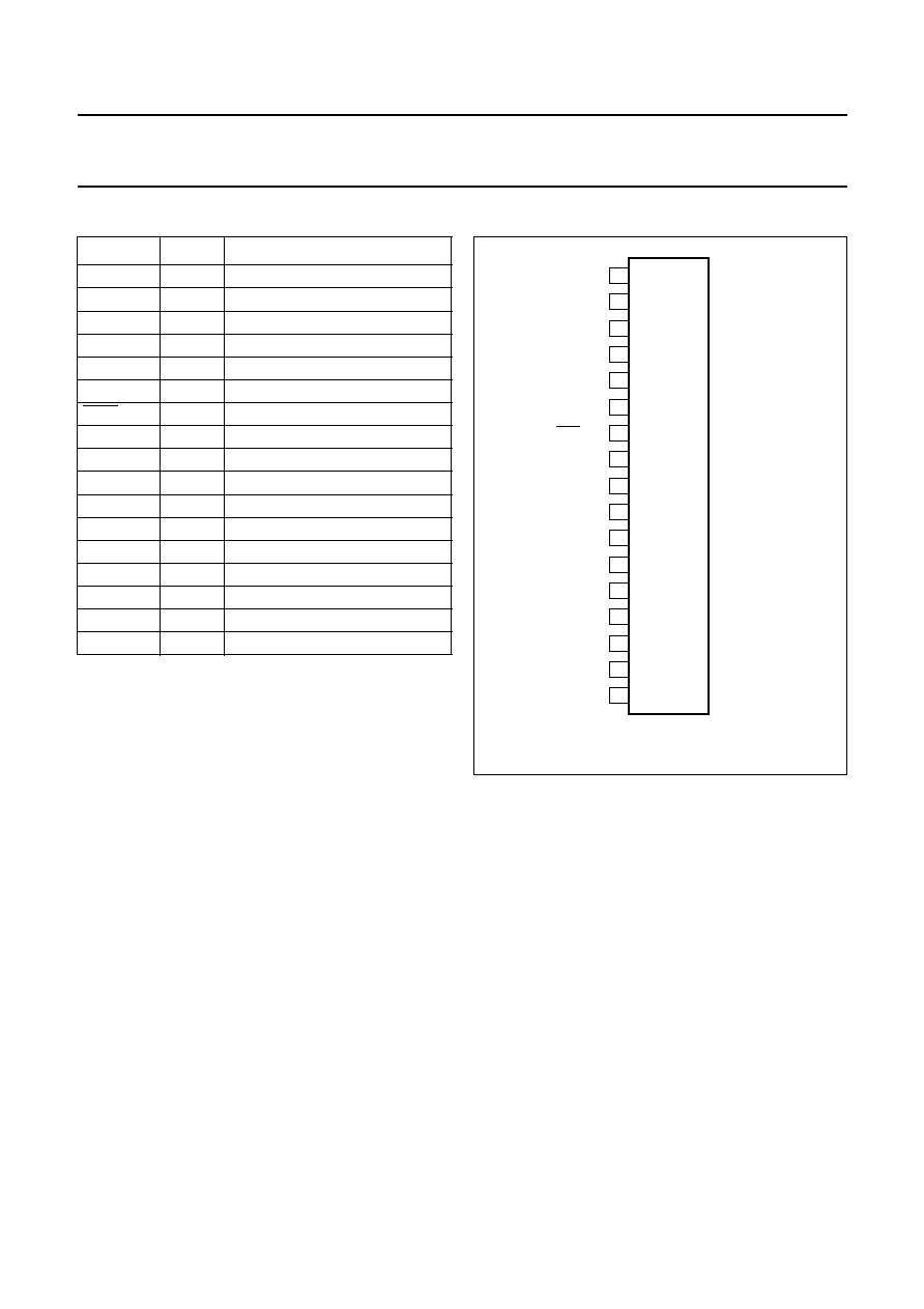
BLOCK DIAGRAM
Fig.1 Block diagram.
handbook, full pagewidth
MGK607
REGULATOR 2
REGULATOR 3
REGULATOR 1
17
16
9
TEMPERATURE
LOAD DUMP
PROTECTION
1
11
4
10
13
14
POWER SWITCH
BACK-UP SWITCH
BACK-UP CONTROL
&
&
&
GND
(14.4 V)
TDA3609JR
RES
REG2
REG3
REG1
(14.2 V/3 A)
(14.2 V/100 mA)
(5 V/100 mA)
(5 V/500 mA)
(10 V/600 mA)
SW
VP
ENSW
EN3
EN1
CRES
BU
HOLD
12
2
IGNITION BUFFER
5
IGN2OUT
IGN2IN
7
INVERTER
6
IGN1IN
8
3
15
Vup = 7, Vfall = 4.5
IGN1OUT
1997 Aug 15
5
Philips Semiconductors
Preliminary specification
Multiple voltage regulator with switch and
ignition buffers
TDA3609JR
PINNING
SYMBOL
PIN
DESCRIPTION
V
P
1
supply voltage
REG1
2
regulator 1 output
REG3
3
regulator 3 output
EN3
4
enable input regulator 3
IGN2
IN
5
ignition 2 input
IGN1
IN
6
ignition 1 input
IGN1
OUT
7
ignition 1 output (active LOW)
IGN2
OUT
8
ignition 2 output
RES
9
reset output
EN1
10
enable input regulator 1
ENSW
11
enable input power switch
HOLD
12
hold output
C
RES
13
reset delay capacitor
GND
14
ground
REG2
15
regulator 2 output
BU
16
back-up
SW
17
power switch output
Fig.2 Pin configuration.
handbook, halfpage
TDA3609JR
MGK606
VP
REG1
REG3
EN3
IGN2IN
IGN1IN
IGN1OUT
IGN2OUT
RES
EN1
ENSW
HOLD
CRES
GND
REG2
BU
SW
1
2
3
4
5
6
7
8
9
10
11
12
13
14
15
16
17
FUNCTIONAL DESCRIPTION
The TDA3609JR is a multiple output voltage regulator with
a power switch, intended for use in car radios with or
without a microcontroller. Because of low-voltage
operation of the car radio, low-voltage drop regulators are
used in the TDA3609JR.
Regulator 2 will switch on when the back-up voltage
exceeds 6.5 V for the first time and will switch off again
when the output voltage of regulator 2 is below 1.9 V (this
is far below an engine start). When regulator 2 is switched
on and the output voltage of this regulator is within its
voltage range, the reset output will be enabled (reset will
go HIGH via a pull-up resistor) to generate a reset to the
microcontroller. The reset cycles can be extended by a
external capacitor at pin 13. The above mentioned start-up
feature is built-in to secure a smooth start-up of the
microcontroller at first connection, without uncontrolled
switching of regulator 2 during the start-up sequence.
The charge of the back-up capacitor can be used to supply
regulator 2 for a short period when the supply falls down
to 0 V (time depends on value of storage capacitor).
The output stages (regulator 1 and 3) of this regulator have
extreme low noise behaviour and good stability. Using
small output capacitors regulator 1 and 3 are made stable.
When both regulator 2 and the supply voltage (V
P
> 4.5 V)
are available, regulators 1 and 3 can be operated by
means of enable inputs (pins 10 and 4 respectively).
Regulator 1 has a hold output (open collector) indicating
that the output voltage of this regulator is settled (held
HIGH by external pull-up resistor). When the output
voltage of this regulator drops out of regulation (because
of supply voltage drop or high load) the hold output will go
LOW. The hold output signal is only valid when regulator 1
is enabled by its enable input (pin 10).
1997 Aug 15
6
Philips Semiconductors
Preliminary specification
Multiple voltage regulator with switch and
ignition buffers
TDA3609JR
The power switch can also be controlled by means of a
separate enable input (pin 11).
All output pins are fully protected. The regulators are
protected against load dump (regulator 1 and 3 will switch
off at supply voltages >18 V) and short-circuit (foldback
current protection).
The switch contains a current protection, but this
protection is delayed at short-circuit condition for at least
10 ms. During this time the output current is limited to a
peak value of at least 3 A and 2 A continuous (V
P
18 V).
At supply voltages >17 V the switch is clamped at
maximum 16 V (to avoid external connected circuitry being
damaged by an overvoltage) and the switch will switch off
at load dump.
By means of two independent ignition Schmitt triggers and
ignition output buffers (one open collector and one
push-pull output), interfacing with the microcontroller can
be accomplished (simple full/semi on/off logic
applications). The ignition 1 output is inverted.
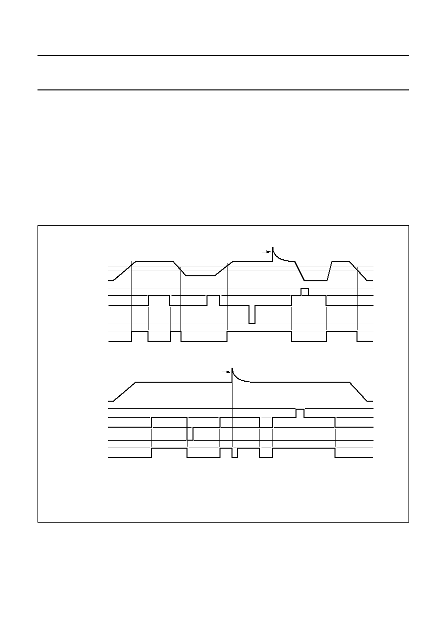
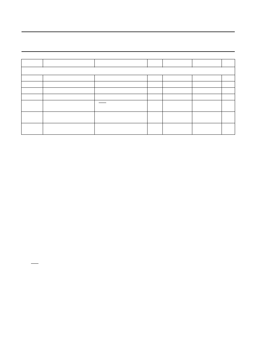
The total timing diagrams are shown in Figs 3 and 4.
Fig.3 Timing diagram ignition Schmitt triggers.
handbook, full pagewidth
load dump
load dump
VP
ignition 1
input
ignition 1
output
VP
ignition 2
input
ignition 2
output
7.0 V
4.5 V
3.25 V
-
100 V
5.0 V
50 V
1.1 V
2.2 V
-
100 V
5.0 V
50 V
2.0 V
Enable Schmitt trigger ignition 1
Enable Schmitt trigger ignition 2
MGK611

1997 Aug 15
7
Philips Semiconductors
Preliminary specification
Multiple voltage regulator with switch and
ignition buffers
TDA3609JR
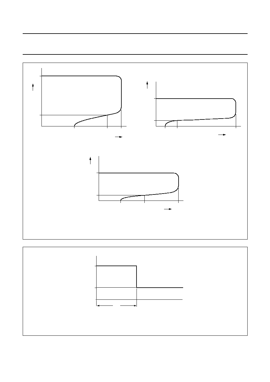
handbook, full pagewidth
VP
VBU
regulator 2
reset
delay
capacitor
reset
VP
enable
regulator 1
regulator 1
regulator 3
enable
regulator 3
VP
enable
power
switch
power
switch
output
6.5 V
5.4 V
5.0 V
1.9 V
0 V
5.0 V
0 V
18 V
10.4 V
7.0 V
4.0 V
2.2 V
10 V
0 V
load dump
5.0 V
0 V
16.9 V
7.0 V
4.0 V
16 V
0 V
3.0 V
6.0 V
2.0 V
2.2 V
2.0 V
2.2 V
2.0 V
load dump
load dump
MGK610
Power switch behaviour
VP and enable Schmitt trigger
Back-up Schmitt trigger and reset behaviour
Fig.4 Timing diagram regulators and power switch.
1997 Aug 15
8
Philips Semiconductors
Preliminary specification
Multiple voltage regulator with switch and
ignition buffers
TDA3609JR
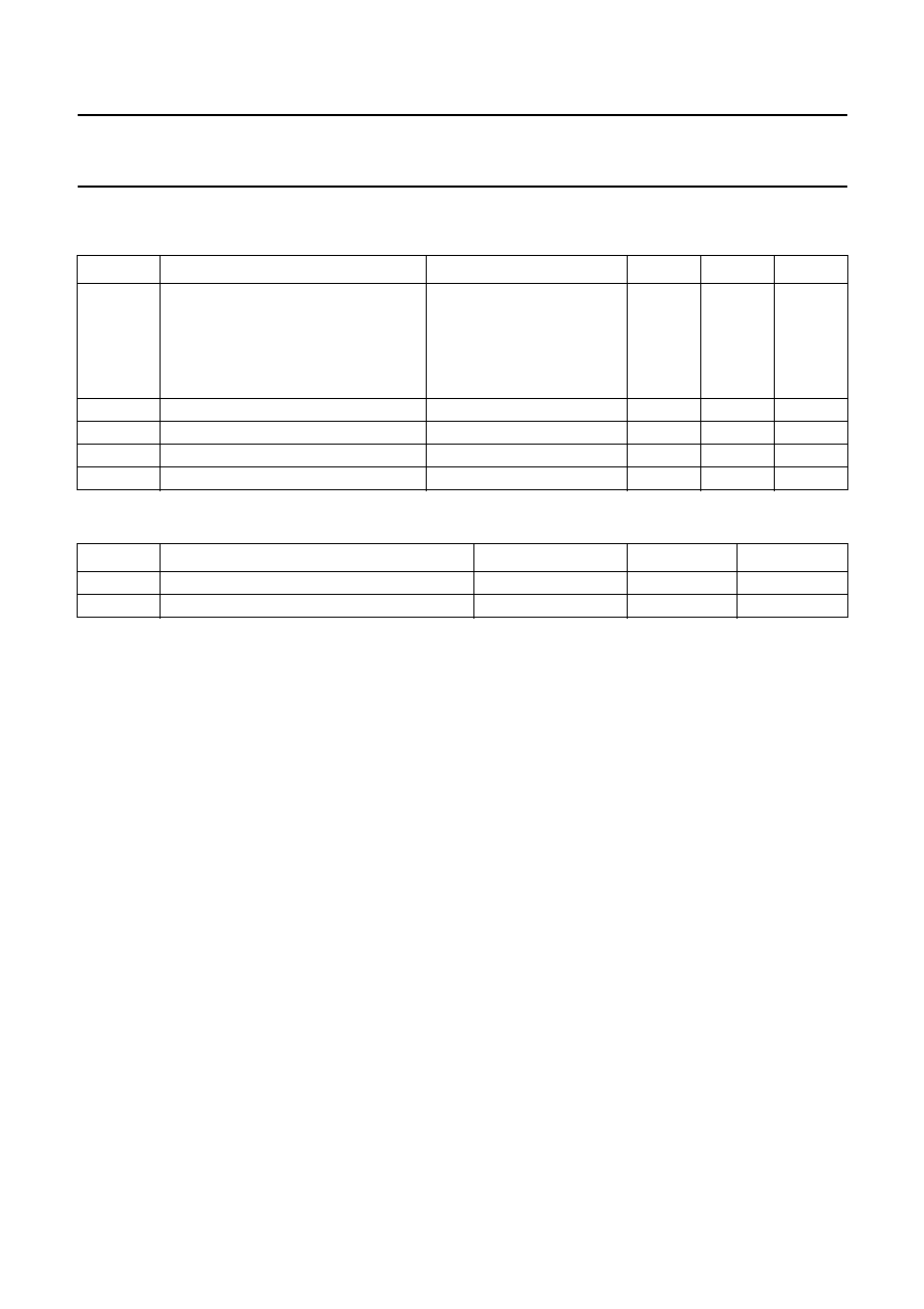
LIMITING VALUES
In accordance with the Absolute Maximum Rating System (IEC 134).
THERMAL CHARACTERISTICS
SYMBOL
PARAMETER
CONDITIONS
MIN.
MAX.
UNIT
V
P
supply voltage
operating
-
18
V
reverse polarity
non-operating
-
-
18
V
jump start
t
10 minutes
-
30
V
load dump protection
t
50 ms; t
r
2.5 ms
-
50
V
P
tot
total power dissipation
-
62
W
T
stg
storage temperature
non-operating
-
55
+150
∞
C
T
amb
ambient temperature
operating
-
40
+85
∞
C
T
j
junction temperature
operating
-
40
+150
∞
C
SYMBOL
PARAMETER
CONDITIONS
VALUE
UNIT
R
th(j-c)
thermal resistance from junction to case
2
K/W
R
th(j-a)
thermal resistance from junction to ambient
in free air
50
K/W

1997 Aug 15
9
Philips Semiconductors
Preliminary specification
Multiple voltage regulator with switch and
ignition buffers
TDA3609JR
CHARACTERISTICS
V
P
= 14.4 V; T
amb
= 25
∞
C; see Fig.7; unless otherwise specified.
SYMBOL
PARAMETER
CONDITIONS
MIN.
TYP.
MAX.
UNIT
Supply
V
P
supply voltage
operating
11
14.4
18
V
regulator 2 on
note 1
2.4
14.4
18
V
jump start
t
10 minutes
-
-
30
V
load dump protection
t
50 ms; t
r
2.5 ms
-
-
50
V
I
q
quiescent supply current
V
P
= 12.4 V; note 2;
I
REG2
= 0.1 mA
-
500
600
µ
A
V
P
= 14.4 V; note 2;
I
REG2
= 0.1 mA
-
520
-
µ
A
Schmitt trigger power supply for switch, regulator 1 and regulator 3
V
thr
rising threshold voltage
6.5
7.0
7.5
V
V
thf
falling threshold voltage
4.0
4.5
5.0
V
V
hys
hysteresis voltage
2.1
2.5
3.3
V
Schmitt trigger for regulator 2
V
thr
rising threshold voltage
6.0
6.5
7.1
V
V
thf
falling threshold voltage
1.7
1.9
2.2
V
V
hys
hysteresis voltage
-
4.6
-
V
Schmitt trigger for enable input (regulator 1, regulator 3 and switch)
V
thr
rising threshold voltage
1.7
2.2
2.7
V
V
thf
falling threshold voltage
1.5
2.0
2.5
V
V
hys
hysteresis voltage
I
REG
= I
sw
= 1 mA
0.1
0.2
0.5
V
I
LI
input leakage current
V
en
= 5 V
1
5
10
µ
A
Reset trigger level
V
thr
rising threshold voltage of
regulator 2
V
P
rising; I
REG1
= 50 mA;
note 3
4.5
V
REG2
-
0.15
V
REG2
-
0.1
V
Schmitt trigger for hold
V
thr
rising threshold voltage of
regulator 1
V
P
rising; note 3
-
V
REG1
-
0.15
V
REG1
-
0.075
V
V
thf
falling threshold voltage of
regulator 1
V
P
falling; note 3
9.2
V
REG1
-
0.35
-
V
V
hys
hysteresis voltage
0.1
0.2
0.3
V
Reset and hold buffer
I
sinkL
LOW-level sink current
V
RES/HOLD
0.8 V
2
-
-
mA
I
LO
output leakage current
V
P
= 14.4 V;
V
RES/HOLD
= 5 V
-
0.1
5
µ
A
rise time
note 4
-
7
50
µ
s
fall time
note 4
-
1
50
µ
s

1997 Aug 15
10
Philips Semiconductors
Preliminary specification
Multiple voltage regulator with switch and
ignition buffers
TDA3609JR
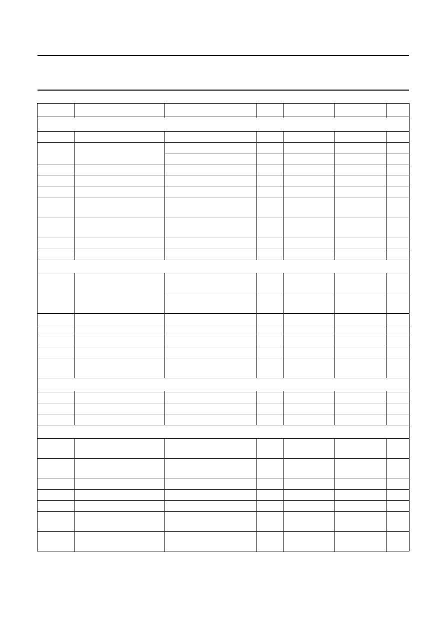
Reset delay
I
ch
charge current
2
4
8
µ
A
I
dch
discharge current
500
800
-
µ
A
V
thr
rising voltage threshold
2.5
3.0
3.5
V
t
d
delay time
C = 47 nF; note 5
20
35
70
ms
Regulator 1 (I
REG1
= 5 mA unless otherwise specified)
V
O(off)
output voltage off
-
1
400
mV
V
O(REG1)
output voltage
1 mA
I
REG1
600 mA
9.5
10.0
10.5
V
12 V
V
P
18 V
9.5
10.0
10.5
V
V
line regulation
12 V
V
P
18 V
-
2
75
mV
V
L
load regulation
1 mA
I
REG1
600 mA
-
20
100
mV
I
q
quiescent current
I
R1
= 600 mA
-
25
60
mA
SVRR
supply voltage ripple
rejection
f
i
= 3 kHz; V
i(p-p)
= 2 V
60
70
-
dB
V
d
drop-out voltage
I
REG1
= 550 mA;
V
P
= 9.5 V; note 6
-
0.4
0.7
V
I
REGm1
current limit
V
REG1
> 8.5 V; note 7
0.65
1.2
-
A
I
REGsc1
short-circuit current
R
L
0.5
; note 8
250
800
-
mA
Regulator 2 (I
REG2
= 5 mA unless otherwise specified)
V
O(REG2)
output voltage
0.5 mA
I
REG2
150 mA
4.75
5.0
5.25
V
I
REG2
= 300 mA; note 9
4.75
5.0
5.25
V
8 V
V
P
18 V
4.75
5.0
5.25
V
18 V
V
P
50 V;
I
REG2
150 mA
4.75
5.0
5.25
V
V
line regulation
6 V
V
P
18 V
-
2
50
mV
6 V
V
P
50 V
-
15
75
mV
V
L
load regulation
1 mA
I
REG2
150 mA
-
20
50
mV
1 mA
I
REG2
300 mA
-
-
100
mV
SVRR
supply voltage ripple
rejection
f = 3 kHz; V
i(p-p)
= 2 V
60
70
-
dB
V
d
drop-out voltage
I
REG2
= 100 mA;
V
P
= 4.75 V; note 6
-
0.4
0.6
V
I
REG2
= 200 mA;
V
P
= 5.75 V; note 6
-
0.8
1.2
V
I
REG2
= 100 mA;
V
bu
= 4.75 V; note 10
-
0.2
0.5
V
I
REG2
= 200 mA;
V
bu
= 5.75 V; note 10
-
0.8
1.0
V
I
REGm2
current limit
V
REG2
> 4.5 V; note 7
0.32
0.37
-
A
I
REGsc2
short-circuit current
R
L
0.5
; note 8
20
100
-
mA
SYMBOL
PARAMETER
CONDITIONS
MIN.
TYP.
MAX.
UNIT
1997 Aug 15
11
Philips Semiconductors
Preliminary specification
Multiple voltage regulator with switch and
ignition buffers
TDA3609JR
Regulator 3 (I
REG3
= 5 mA unless otherwise specified)
V
O(off)
output voltage off
-
1
400
mV
V
O(REG3)
output voltage
1 mA
I
REG3
500 mA
4.75
5.0
5.25
V
7 V
V
P
18 V
4.75
5.0
5.25
V
V
line regulation
7 V
V
P
18 V
-
2
50
mV
V
L
load regulation
1 mA
I
REG3
500 mA
-
20
75
mV
I
q
quiescent current
I
R3
= 500 mA
-
19
45
mA
SVRR
supply voltage ripple
rejection
f
i
= 3 kHz; V
i(p-p)
= 2 V
60
70
-
dB
V
d
drop-out voltage
I
REG3
= 500 mA;
V
P
= 5.75 V; note 6
-
1
1.5
V
I
REGm3
current limit
V
REG3
> 4.5 V; note 7
0.60
0.80
-
A
I
REGsc3
short-circuit current
R
L
0.5
; note 8
100
400
-
mA
Power switch
V
d
drop-out voltage
I
sw
= 1 A; V
P
= 13.5 V;
note 11
-
0.6
0.85
V
I
sw
= 1.8 A; V
P
= 13.5 V;
note 11
-
1.4
1.9
V
I
dc
continuous current
V
P
= 16 V; V
sw
= 13.5 V
1.8
2.0
-
A
V
cl
clamping voltage
V
P
17 V
13.5
15.0
16.0
V
I
M
peak current
V
P
= 17 V; notes 12 and 13
3
-
-
A
V
fb
fly back voltage behaviour
I
sw
=
-
100 mA
-
V
P
+ 3
22
V
I
sc
short-circuit current
V
P
= 14.4 V; V
sw
< 1.2 V;
note 13
-
0.8
-
A
Back-up switch
I
dc
continuous current
0.3
0.35
-
A
V
cl
clamping voltage
V
P
16.7 V
-
-
16
V
I
r
reverse current
V
P
= 0 V; V
bu
= 12.4 V
-
-
900
mA
Schmitt trigger for enable input of ignition 1
V
thr
rising threshold voltage of
ignition 1 input
2.75
3.25
3.75
V
V
thf
falling threshold voltage of
ignition 1 input
0.8
-
1.3
V
V
hys
hysteresis voltage
1.5
-
-
V
I
LI
input leakage current
V
IGN1in
= 5 V
-
-
1.0
µ
A
I
I(clamp)
input clamping current
V
IGN1in
> 50 V
-
-
50
mA
V
IH(clamp)
HIGH-level input clamping
voltage
V
P
-
50
V
V
IL(clamp)
LOW-level input clamping
voltage
-
0.6
-
0
V
SYMBOL
PARAMETER
CONDITIONS
MIN.
TYP.
MAX.
UNIT
1997 Aug 15
12
Philips Semiconductors
Preliminary specification
Multiple voltage regulator with switch and
ignition buffers
TDA3609JR
Schmitt trigger power supply for ignition 1
V
thr
rising threshold voltage
6.5
7.0
7.5
V
V
thf
falling threshold voltage
note 14
4.0
4.5
5.0
V
Ignition 1 buffer
V
OL
LOW-level output voltage
I
IGN1out
= 0 mA
0
0.2
0.8
V
I
OL
LOW-level output current
V
IGN1out
0.8 V
0.45
0.8
-
mA
I
LO
output leakage current
V
IGN1out
= 5 V; V
IGN1in
= 0 V
-
-
1.0
µ
A
t
PLH
LOW-to-HIGH
propagation time
V
IGN1in
rising from
0.8 V to 3.75 V
-
-
500
µ
s
t
PHL
HIGH-to-LOW
propagation time
V
IGN1in
falling from
3.75 V to 0.8 V
-
-
500
µ
s
Schmitt trigger for enable input of ignition 2
V
thr
rising threshold voltage of
ignition 2 input
V
P
> 3.5 V
1.9
2.2
2.5
V
V
thf
falling threshold voltage of
ignition 2 input
V
P
> 3.5 V
1.7
2.0
2.3
V
V
hys
hysteresis voltage
V
P
> 3.5 V
0.1
0.2
0.5
V
I
LI
input leakage current
V
IGN2in
= 5 V
-
-
1.0
µ
A
I
I(clamp)
input clamp current
V
IGN2in
> 50 V
-
-
50
mA
V
IH(clamp)
HIGH-level input clamping
voltage
V
P
-
50
V
V
IL(clamp)
LOW-level input clamping
voltage
-
0.6
-
0
V
SYMBOL
PARAMETER
CONDITIONS
MIN.
TYP.
MAX.
UNIT
1997 Aug 15
13
Philips Semiconductors
Preliminary specification
Multiple voltage regulator with switch and
ignition buffers
TDA3609JR
Notes
1. Minimum operating voltage, only if V
P
has exceeded 6.5 V.
2. The quiescent current is measured in the standby mode. So, the enable inputs of regulator 1, 3 and the power switch
are grounded and R
L(REG2)
=
(see Fig.7).
3. The voltage of the regulator sinks as a result of a V
P
drop.
4. The rise and fall time is measured with a 10 k
pull-up resistor and a 50 pF load capacitor.
5. The delay time depends on the value of the capacitor:
6. The drop-out voltage of regulators 1, 2 and 3 is measured between V
P
and REGn.
7. At current limit, I
REGmn
is held constant (see Fig.5 for behaviour of I
REGmn
).
8. The foldback current protection limits the dissipated power at short-circuit (see Fig.5).
9. The peak current of 300 mA can only be applied for short periods (t < 100 ms).
10. The drop-out voltage measured between BU and REG2.
11. The drop-out voltage of the power switch is measured between V
P
and SW.
12. The maximum output current of the switch is limited to 1.8 A when the supply voltage exceeds 18 V.
A test-mode is built-in. The delay time of the switch will be disabled when a voltage of V
P
+ 1 V is applied to the
switch-enable input.
13. At short-circuit, I
sc
of the power switch is held constant to a lower value than the continuous current after a delay of
at least 10 ms. A test-mode is built-in. The delay time of the switch will be disabled when a voltage of V
P
+ 1 V is
applied to the switch-enable input.
14. V
IGN1out
= LOW for V
IGN1out
> 1.2 V or V
EN1
> 1.3 V or V
EN3
> 1.3 V or V
ENSW
> 1.3 V.
Ignition 2 buffer
V
OL
LOW-level output voltage
I
IGN2out
= 0 mA
0
0.2
0.8
V
V
OH
HIGH-level output voltage
I
IGN2out
= 0 mA
4.5
5.0
5.25
V
I
OL
LOW-level output current
V
IGN2out
0.8 V
0.45
0.8
-
mA
I
OH
HIGH-level output current
V
IGN2out
4.5 V
-
0.45
-
2.0
-
mA
I
LO
output leakage current
(source)
V
IGN1out
= 5 V; V
IGN1in
= 0 V
-
-
1.0
µ
A
t
PLH
LOW-to-HIGH
propagation time
V
IGN2in
rising from
1.7 V to 2.5 V
-
-
500
µ
s
t
PHL
HIGH-to-LOW
propagation time
V
IGN2in
falling from
2.5 V to 1.7 V
-
-
500
µ
s
SYMBOL
PARAMETER
CONDITIONS
MIN.
TYP.
MAX.
UNIT
t
d
C
I
ch
------
V
C(th)
◊
C
750
10
3
◊
◊
ms
(
)
=
=
1997 Aug 15
14
Philips Semiconductors
Preliminary specification
Multiple voltage regulator with switch and
ignition buffers
TDA3609JR
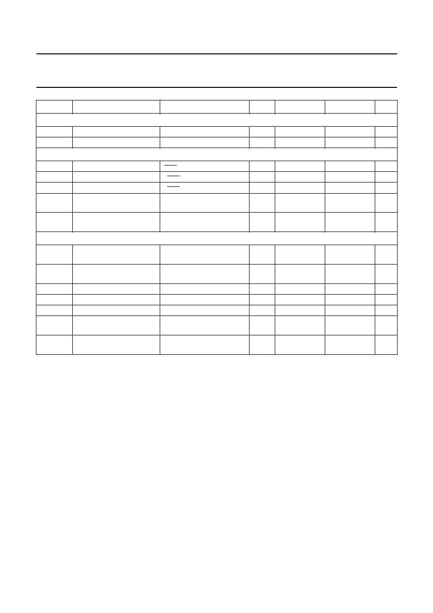
Fig.5 Foldback current protection of the regulators.
a. Regulator 1.
b. Regulator 2.
c. Regulator 3.
handbook, halfpage
300 mA
MGK608
10 V
2 V
IREGsc1
IREG1
IREGm1
VO(REG1)
handbook, halfpage
50 mA
MGK655
5.0 V
1 V
IREGsc2
IREG2
IREGm2
VO(REG2)
handbook, halfpage
200 mA
MGK656
5.0 V
1 V
IREGsc3
IREG3
IREGm3
VO(REG3)
Fig.6 Current protection of the power switch.
handbook, halfpage
MGB758
3
10
1.8
t (ms)
Isw
(A)
V
SW
> 5 V.

1997 Aug 15
15
Philips Semiconductors
Preliminary specification
Multiple voltage regulator with switch and
ignition buffers
TDA3609JR
TEST AND APPLICATION INFORMATION
Test information
Fig.7 Test circuit.
handbook, full pagewidth
MGK609
enable input regulator 3
reset delay
capacitor
reset
output
C3
10
µ
F
C2
220 nF
C1
220 nF
C4
10
µ
F
ignition 1
output
ignition 2
output
R2
10 k
RL(REG2)
5 k
RL(SW)
12 k
5 V
5 V
10 V
regulator 3
output
regulator 1
output
regulator 2
output
C5
10
µ
F
C6
1
µ
F
C7
47 nF
RL(REG1)
10 k
RL(REG3)
5 k
power switch output
17
15
2
7
8
hold
output
12
9
3
4
13
16
11
1
14
TDA3609JR
ground
VP
supply voltage
VENSW
VEN3
enable input regulator 1
enable input power switch
10
VEN1
back-up
ignition 2
input
10 k
R6
C10
1 nF
ignition 1
input
5
6
VIGN 2
10 k
R5
C9
1 nF
VIGN1
C8
Vbu
R3
10 k
R4
10 k
1997 Aug 15
16
Philips Semiconductors
Preliminary specification
Multiple voltage regulator with switch and
ignition buffers
TDA3609JR
Application information
N
OISE
Table 1
Noise figures
Note
1. Measured at a bandwidth of 200 kHz.
The noise on the supply line depends on the value of the
supply capacitor and is caused by a current noise (output
noise of the regulators is translated into a current noise by
means of the output capacitors). When a high frequency
capacitor of 220 nF in parallel with an electrolytic capacitor
of 100
µ
F is connected directly to pins 1 and 14 (supply
and ground) the noise is minimal.
S
TABILITY
The regulators are made stable with the external
connected output capacitors.
REGULATOR
NOISE FIGURE (
µ
V)
(1)
C
O
= 10
µ
F
C
O
= 47
µ
F
C
O
= 100
µ
F
1
tbf
150
tbf
2
tbf
150
tbf
3
tbf
200
tbf
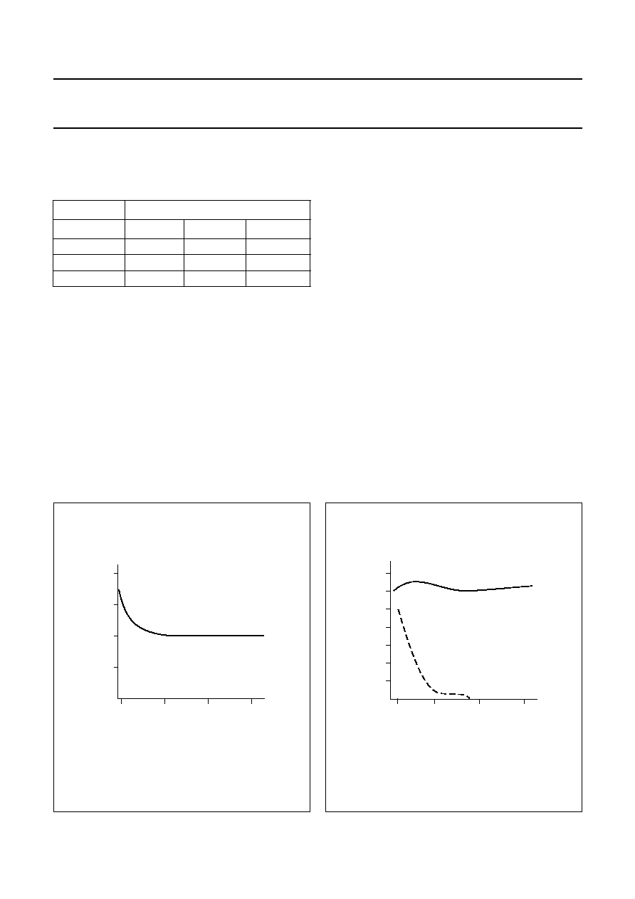
The output capacitors can be selected using the graphs of
Figs 8 and 9. When an electrolytic capacitor is used, the
temperature behaviour of this output capacitor can cause
oscillations at a low temperature. The next 2 examples
show how an output capacitor value is selected.
Example 1
Regulators 1 and 3 are made stable with an electrolytic
output capacitor of 220
µ
F (ESR = 0.15
). At
-
30
∞
C the
capacitor value is decreased to 73
µ
F and the ESR is
increased to 1.1
. The regulator will remain stable at
-
30
∞
C.
Example 2
Regulator 2 is made stable with a 10
µ
F electrolytic
capacitor (ESR = 3
). At
-
30
∞
C the capacitor value is
decreased to 3
µ
F and the ESR is increased to 23.1
.
Using Fig.9, the regulator will be instable at
-
30
∞
C.
Solution
Use a tantalum capacitor of 10
µ
F or a larger electrolytic
capacitor. To avoid problems with stability at low
temperatures, the use of tantalum capacitors is
recommended.
handbook, halfpage
0
0.1
1
10
C (
µ
F)
MGK612
stable region
maximum ESR
100
R
(
)
20
15
10
5
Fig.8
Curve for selecting the value of output
capacitor for regulators 1 and 3.
handbook, halfpage
2
0
0.22
1
10
C (
µ
F)
MGK613
4
6
8
10
12
stable region
maximum ESR
minimum ESR
100
R
(
)
14
Fig.9
Curve for selecting the value of output
capacitor for regulator 2.
1997 Aug 15
17
Philips Semiconductors
Preliminary specification
Multiple voltage regulator with switch and
ignition buffers
TDA3609JR
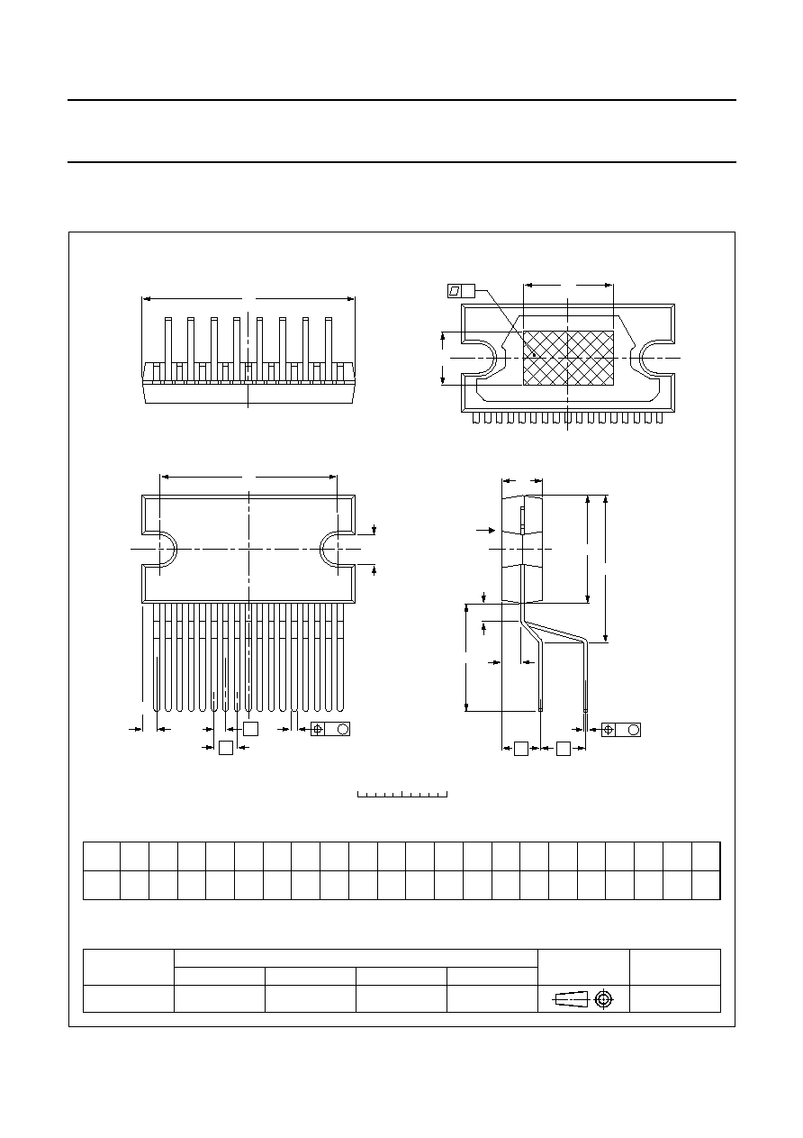
PACKAGE OUTLINE
REFERENCES
OUTLINE
VERSION
EUROPEAN
PROJECTION
ISSUE DATE
97-05-20
IEC
JEDEC
EIAJ
DIMENSIONS (mm are the original dimensions)
Note
1. Plastic or metal protrusions of 0.25 mm maximum per side are not included.
SOT475-1
0
5
10 mm
scale
D
L
E
A
c
A
2
L
3
Q
w
M
b
p
1
d
D
Z
e
e
x
h
1
17
j
Eh
non-concave
DBS17P: plastic DIL-bent-SIL (special bent) power package; 17 leads (lead length 12 mm)
SOT475-1
view B: mounting base side
m
2
e
v
M
B
UNIT
A
e
1
A
2
b
p
c
D
(1)
E
(1)
Z
(1)
d
e
D
h
L
L
3
m
mm
17.0
15.5
4.6
4.2
0.75
0.60
0.48
0.38
24.0
23.6
20.0
19.6
10
2.54
v
0.8
12.2
11.8
1.27
e
2
5.08
2.4
1.6
E
h
6
2.00
1.45
2.1
1.8
3.4
3.1
4.3
12.4
11.0
Q
j
0.4
w
0.03
x

1997 Aug 15
18
Philips Semiconductors
Preliminary specification
Multiple voltage regulator with switch and
ignition buffers
TDA3609JR
SOLDERING
Introduction
There is no soldering method that is ideal for all IC
packages. Wave soldering is often preferred when
through-hole and surface mounted components are mixed
on one printed-circuit board. However, wave soldering is
not always suitable for surface mounted ICs, or for
printed-circuits with high population densities. In these
situations reflow soldering is often used.
This text gives a very brief insight to a complex technology.
A more in-depth account of soldering ICs can be found in
our
"IC Package Databook" (order code 9398 652 90011).
Soldering by dipping or by wave
The maximum permissible temperature of the solder is
260
∞
C; solder at this temperature must not be in contact
with the joint for more than 5 seconds. The total contact
time of successive solder waves must not exceed
5 seconds.
The device may be mounted up to the seating plane, but
the temperature of the plastic body must not exceed the
specified maximum storage temperature (T
stg max
). If the
printed-circuit board has been pre-heated, forced cooling
may be necessary immediately after soldering to keep the
temperature within the permissible limit.
Repairing soldered joints
Apply a low voltage soldering iron (less than 24 V) to the
lead(s) of the package, below the seating plane or not
more than 2 mm above it. If the temperature of the
soldering iron bit is less than 300
∞
C it may remain in
contact for up to 10 seconds. If the bit temperature is
between 300 and 400
∞
C, contact may be up to 5 seconds.
DEFINITIONS
LIFE SUPPORT APPLICATIONS
These products are not designed for use in life support appliances, devices, or systems where malfunction of these
products can reasonably be expected to result in personal injury. Philips customers using or selling these products for
use in such applications do so at their own risk and agree to fully indemnify Philips for any damages resulting from such
improper use or sale.
Data sheet status
Objective specification
This data sheet contains target or goal specifications for product development.
Preliminary specification
This data sheet contains preliminary data; supplementary data may be published later.
Product specification
This data sheet contains final product specifications.
Limiting values
Limiting values given are in accordance with the Absolute Maximum Rating System (IEC 134). Stress above one or
more of the limiting values may cause permanent damage to the device. These are stress ratings only and operation
of the device at these or at any other conditions above those given in the Characteristics sections of the specification
is not implied. Exposure to limiting values for extended periods may affect device reliability.
Application information
Where application information is given, it is advisory and does not form part of the specification.

1997 Aug 15
19
Philips Semiconductors
Preliminary specification
Multiple voltage regulator with switch and
ignition buffers
TDA3609JR
NOTES

Internet: http://www.semiconductors.philips.com
Philips Semiconductors ≠ a worldwide company
© Philips Electronics N.V. 1997
SCA55
All rights are reserved. Reproduction in whole or in part is prohibited without the prior written consent of the copyright owner.
The information presented in this document does not form part of any quotation or contract, is believed to be accurate and reliable and may be changed
without notice. No liability will be accepted by the publisher for any consequence of its use. Publication thereof does not convey nor imply any license
under patent- or other industrial or intellectual property rights.
Netherlands: Postbus 90050, 5600 PB EINDHOVEN, Bldg. VB,
Tel. +31 40 27 82785, Fax. +31 40 27 88399
New Zealand: 2 Wagener Place, C.P.O. Box 1041, AUCKLAND,
Tel. +64 9 849 4160, Fax. +64 9 849 7811
Norway: Box 1, Manglerud 0612, OSLO,
Tel. +47 22 74 8000, Fax. +47 22 74 8341
Philippines: Philips Semiconductors Philippines Inc.,
106 Valero St. Salcedo Village, P.O. Box 2108 MCC, MAKATI,
Metro MANILA, Tel. +63 2 816 6380, Fax. +63 2 817 3474
Poland: Ul. Lukiska 10, PL 04-123 WARSZAWA,
Tel. +48 22 612 2831, Fax. +48 22 612 2327
Portugal: see Spain
Romania: see Italy
Russia: Philips Russia, Ul. Usatcheva 35A, 119048 MOSCOW,
Tel. +7 095 755 6918, Fax. +7 095 755 6919
Singapore: Lorong 1, Toa Payoh, SINGAPORE 1231,
Tel. +65 350 2538, Fax. +65 251 6500
Slovakia: see Austria
Slovenia: see Italy
South Africa: S.A. PHILIPS Pty Ltd., 195-215 Main Road Martindale,
2092 JOHANNESBURG, P.O. Box 7430 Johannesburg 2000,
Tel. +27 11 470 5911, Fax. +27 11 470 5494
South America: Rua do Rocio 220, 5th floor, Suite 51,
04552-903 S„o Paulo, S√O PAULO - SP, Brazil,
Tel. +55 11 821 2333, Fax. +55 11 829 1849
Spain: Balmes 22, 08007 BARCELONA,
Tel. +34 3 301 6312, Fax. +34 3 301 4107
Sweden: Kottbygatan 7, Akalla, S-16485 STOCKHOLM,
Tel. +46 8 632 2000, Fax. +46 8 632 2745
Switzerland: Allmendstrasse 140, CH-8027 ZÐRICH,
Tel. +41 1 488 2686, Fax. +41 1 481 7730
Taiwan: Philips Semiconductors, 6F, No. 96, Chien Kuo N. Rd., Sec. 1,
TAIPEI, Taiwan Tel. +886 2 2134 2865, Fax. +886 2 2134 2874
Thailand: PHILIPS ELECTRONICS (THAILAND) Ltd.,
209/2 Sanpavuth-Bangna Road Prakanong, BANGKOK 10260,
Tel. +66 2 745 4090, Fax. +66 2 398 0793
Turkey: Talatpasa Cad. No. 5, 80640 GÐLTEPE/ISTANBUL,
Tel. +90 212 279 2770, Fax. +90 212 282 6707
Ukraine: PHILIPS UKRAINE, 4 Patrice Lumumba str., Building B, Floor 7,
252042 KIEV, Tel. +380 44 264 2776, Fax. +380 44 268 0461
United Kingdom: Philips Semiconductors Ltd., 276 Bath Road, Hayes,
MIDDLESEX UB3 5BX, Tel. +44 181 730 5000, Fax. +44 181 754 8421
United States: 811 East Arques Avenue, SUNNYVALE, CA 94088-3409,
Tel. +1 800 234 7381
Uruguay: see South America
Vietnam: see Singapore
Yugoslavia: PHILIPS, Trg N. Pasica 5/v, 11000 BEOGRAD,
Tel. +381 11 625 344, Fax.+381 11 635 777
For all other countries apply to: Philips Semiconductors, Marketing & Sales Communications,
Building BE-p, P.O. Box 218, 5600 MD EINDHOVEN, The Netherlands, Fax. +31 40 27 24825
Argentina: see South America
Australia: 34 Waterloo Road, NORTH RYDE, NSW 2113,
Tel. +61 2 9805 4455, Fax. +61 2 9805 4466
Austria: Computerstr. 6, A-1101 WIEN, P.O. Box 213, Tel. +43 160 1010,
Fax. +43 160 101 1210
Belarus: Hotel Minsk Business Center, Bld. 3, r. 1211, Volodarski Str. 6,
220050 MINSK, Tel. +375 172 200 733, Fax. +375 172 200 773
Belgium: see The Netherlands
Brazil: see South America
Bulgaria: Philips Bulgaria Ltd., Energoproject, 15th floor,
51 James Bourchier Blvd., 1407 SOFIA,
Tel. +359 2 689 211, Fax. +359 2 689 102
Canada: PHILIPS SEMICONDUCTORS/COMPONENTS,
Tel. +1 800 234 7381
China/Hong Kong: 501 Hong Kong Industrial Technology Centre,
72 Tat Chee Avenue, Kowloon Tong, HONG KONG,
Tel. +852 2319 7888, Fax. +852 2319 7700
Colombia: see South America
Czech Republic: see Austria
Denmark: Prags Boulevard 80, PB 1919, DK-2300 COPENHAGEN S,
Tel. +45 32 88 2636, Fax. +45 31 57 0044
Finland: Sinikalliontie 3, FIN-02630 ESPOO,
Tel. +358 9 615800, Fax. +358 9 61580920
France: 4 Rue du Port-aux-Vins, BP317, 92156 SURESNES Cedex,
Tel. +33 1 40 99 6161, Fax. +33 1 40 99 6427
Germany: Hammerbrookstraþe 69, D-20097 HAMBURG,
Tel. +49 40 23 53 60, Fax. +49 40 23 536 300
Greece: No. 15, 25th March Street, GR 17778 TAVROS/ATHENS,
Tel. +30 1 4894 339/239, Fax. +30 1 4814 240
Hungary: see Austria
India: Philips INDIA Ltd, Band Box Building, 2nd floor,
254-D, Dr. Annie Besant Road, Worli, MUMBAI 400 025,
Tel. +91 22 493 8541, Fax. +91 22 493 0966
Indonesia: see Singapore
Ireland: Newstead, Clonskeagh, DUBLIN 14,
Tel. +353 1 7640 000, Fax. +353 1 7640 200
Israel: RAPAC Electronics, 7 Kehilat Saloniki St, PO Box 18053,
TEL AVIV 61180, Tel. +972 3 645 0444, Fax. +972 3 649 1007
Italy: PHILIPS SEMICONDUCTORS, Piazza IV Novembre 3,
20124 MILANO, Tel. +39 2 6752 2531, Fax. +39 2 6752 2557
Japan: Philips Bldg 13-37, Kohnan 2-chome, Minato-ku, TOKYO 108,
Tel. +81 3 3740 5130, Fax. +81 3 3740 5077
Korea: Philips House, 260-199 Itaewon-dong, Yongsan-ku, SEOUL,
Tel. +82 2 709 1412, Fax. +82 2 709 1415
Malaysia: No. 76 Jalan Universiti, 46200 PETALING JAYA, SELANGOR,
Tel. +60 3 750 5214, Fax. +60 3 757 4880
Mexico: 5900 Gateway East, Suite 200, EL PASO, TEXAS 79905,
Tel. +9-5 800 234 7381
Middle East: see Italy
Printed in The Netherlands
547027/1200/01/pp20
Date of release: 1997 Aug 15
Document order number:
9397 750 02248