 | –≠–ª–µ–∫—Ç—Ä–æ–Ω–Ω—ã–π –∫–æ–º–ø–æ–Ω–µ–Ω—Ç: TDA3618JR | –°–∫–∞—á–∞—Ç—å:  PDF PDF  ZIP ZIP |

DATA SHEET
Preliminary specification
Supersedes data of 1999 Jul 13
File under Integrated Circuits, IC01
1999 Sep 01
INTEGRATED CIRCUITS
TDA3618JR
Multiple voltage regulator with
switch and ignition buffers

1999 Sep 01
2
Philips Semiconductors
Preliminary specification
Multiple voltage regulator with switch and
ignition buffers
TDA3618JR
FEATURES
General
∑
Extremely low noise behaviour and good stability with
very small output capacitors
∑
Two V
P
-state controlled regulators (regulators 1 and 3)
and a power switch
∑
Regulator 2, reset and ignition buffer operate during
load dump and thermal shutdown
∑
Separate control pins for switching regulators
(regulators 1 and 3) and the power switch
∑
Supply voltage range of
-
18 to +50 V
∑
Low reverse current of regulator 2
∑
Low quiescent current (when regulator 1, regulator 3
and power switch are switched off)
∑
Hold output for low V
P
(regulators 1 and 3 off)
∑
Hold output for regulators 1 and 3
∑
Hold output for foldback mode switch
∑
Hold output for load dump and temperature protection
∑
Reset and hold outputs (open collector outputs)
∑
Adjustable reset delay time
∑
High ripple rejection
∑
backup capacitor for regulator 2
∑
Two independent ignition buffers (one inverted and with
open collector output).
Protections
∑
Reverse polarity safe (down to
-
18 V without high
reverse current)
∑
Able to withstand voltages up to 18 V at the outputs
(supply line may be short circuited)
∑
ESD protected on all pins
∑
Thermal protections with hysteresis
∑
Load dump protection
∑
Foldback current limit protection for
regulators 1, 2 and 3
∑
Delayed second current limit protection for the power
switch (at short circuit)
∑
The regulator outputs and the power switch are DC
short circuited safe to ground and V
P
.
GENERAL DESCRIPTION
The TDA3618JR is a multiple output voltage regulator with
a power switch and ignition buffers, intended for use in car
radios with or without a microcontroller. It contains:
∑
Two fixed voltage regulators with a foldback current
protection (regulators 1 and 3) and one fixed voltage
regulator (regulator 2), intended to supply a
microcontroller, which also operates during load dump
and thermal shutdown
∑
A power switch with protections, operated by an enable
input
∑
Reset and hold outputs that can be used to interface
with the microcontroller. The reset signal can be used to
call up the microcontroller.
∑
A supply pin which can withstand load dump pulses and
negative supply voltages
∑
Regulator 2, which is switched on at a backup voltage
greater than 6.5 V and off when the output voltage of
regulator 2 drops below 1.9 V
∑
A provision for the use of a reserve supply capacitor that
will hold enough energy for regulator 2 (5 V continuous)
to allow a microcontroller to prepare for loss of voltage
∑
An inverted ignition 1 input with open collector output
stage
∑
An ignition 2 input Schmitt trigger with push-pull output
stage.
ORDERING INFORMATION
TYPE
NUMBER
PACKAGE
NAME
DESCRIPTION
VERSION
TDA3618JR
DBS17P
plastic DIL-bent-SIL (specially bent) power package;
17 leads (lead length 12 mm)
SOT475-1
1999 Sep 01
3
Philips Semiconductors
Preliminary specification
Multiple voltage regulator with switch and
ignition buffers
TDA3618JR
QUICK REFERENCE DATA
SYMBOL
PARAMETER
CONDITIONS
MIN.
TYP.
MAX.
UNIT
Supply
V
P
supply voltage
operating
11
14.4
18
V
reverse polarity
non-operating
-
-
18
V
regulator 2 on
2.4
14.4
50
V
jump start
t
10 minutes
-
-
30
V
load dump protection
t
50 ms; t
r
2.5 ms
-
-
50
V
I
q(tot)
total quiescent supply current
standby mode
-
310
400
µ
A
T
j
junction temperature
-
-
150
∞
C
Voltage regulators
V
O(REG1)
output voltage of regulator 1
1 mA
I
REG1
600 mA
8.5
9.0
9.5
V
V
O(REG2)
output voltage of regulator 2
0.5 mA
I
REG2
150 mA; V
P
= 14.4 V
4.75
5.0
5.25
V
V
O(REG3)
output voltage of regulator 3
1 mA
I
REG3
750 mA
4.75
5.0
5.25
V
Power switch
V
d
drop-out voltage
I
SW
= 1 A
-
0.45
0.7
V
I
SW
= 1.8 A
-
1
1.8
V
I
M
peak current
3
-
-
A

1999 Sep 01
4
Philips Semiconductors
Preliminary specification
Multiple voltage regulator with switch and
ignition buffers
TDA3618JR
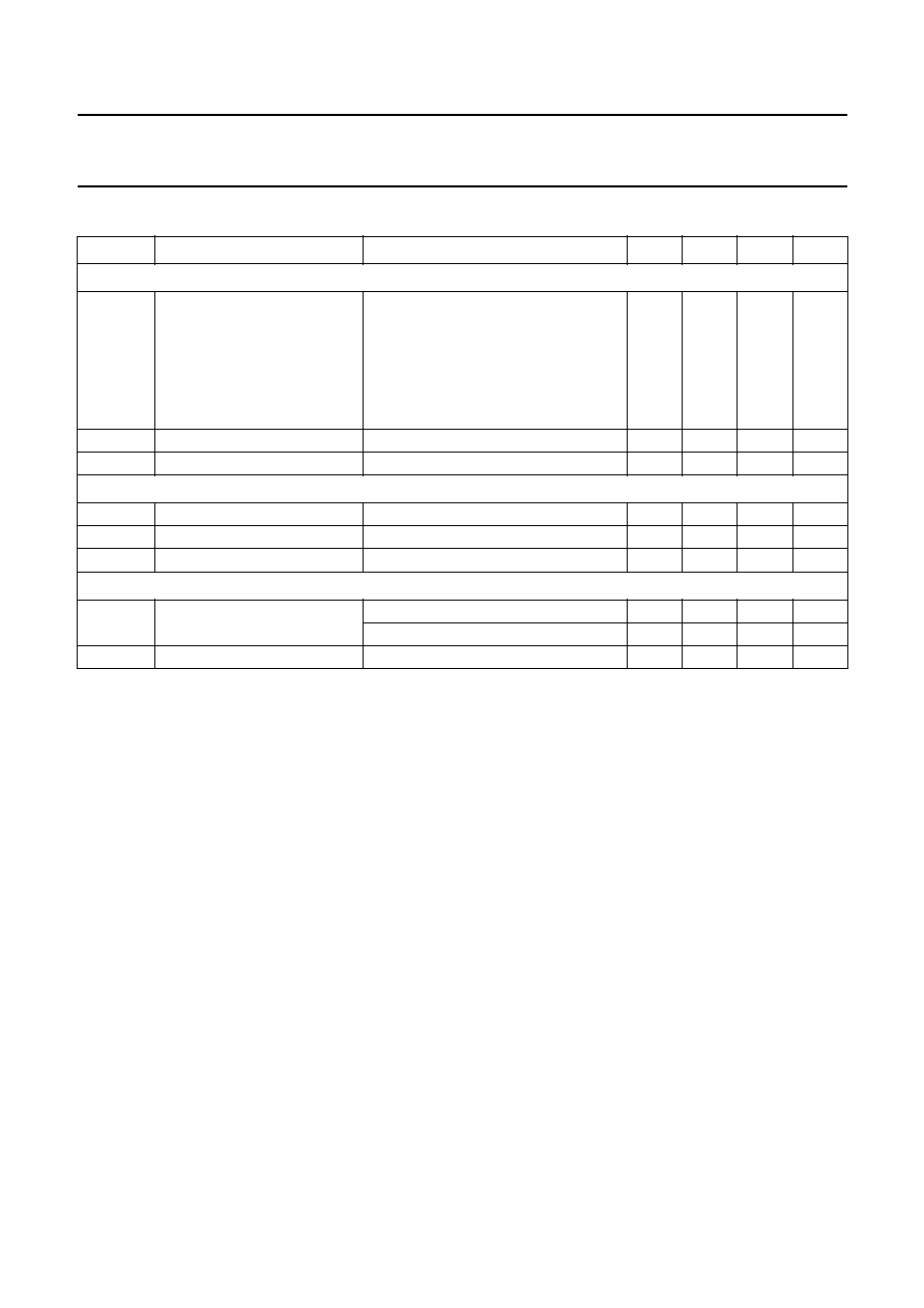
BLOCK DIAGRAM
handbook, full pagewidth
MGR928
REGULATOR 2
REGULATOR 3
REGULATOR 1
17
16
9
TEMPERATURE
LOAD DUMP
PROTECTION
1
11
4
10
13
14
POWER SWITCH
BACK-UP SWITCH
BACK-UP CONTROL
&
&
&
&
1
GND
(14.4 V)
TDA3618JR
RES
REG2
REG3
REG1
(14.2 V/3 A)
(14.2 V/100 mA)
(5 V/150 mA)
(5 V/750 mA)
(9 V/600 mA)
SW
VP
ENSW
EN3
EN1
CRES
BU
HOLD
12
2
IGNITION BUFFER
5
IGN2OUT
IGN2IN
7
INVERTER
6
IGN1IN
8
3
15
Vthr = 7 V, Vthf = 4.5 V
IGN1OUT
Fig.1 Block diagram.
1999 Sep 01
5
Philips Semiconductors
Preliminary specification
Multiple voltage regulator with switch and
ignition buffers
TDA3618JR
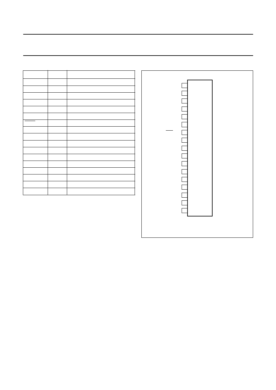
PINNING
SYMBOL
PIN
DESCRIPTION
V
P
1
supply voltage
REG1
2
regulator 1 output
REG3
3
regulator 3 output
EN3
4
enable input regulator 3
IGN2
IN
5
ignition 2 input
IGN1
IN
6
ignition 1 input
IGN1
OUT
7
ignition 1 output (active LOW)
IGN2
OUT
8
ignition 2 output
RES
9
reset output
EN1
10
enable input regulator 1
ENSW
11
enable input power switch
HOLD
12
hold output (active LOW)
C
RES
13
reset delay capacitor
GND
14
ground
REG2
15
regulator 2 output
BU
16
backup
SW
17
power switch output
Fig.2 Pin configuration.
handbook, halfpage
TDA3618JR
MGR929
VP
REG1
REG3
EN3
IGN2IN
IGN1IN
IGN1OUT
IGN2OUT
RES
EN1
ENSW
HOLD
CRES
GND
REG2
BU
SW
1
2
3
4
5
6
7
8
9
10
11
12
13
14
15
16
17

1999 Sep 01
6
Philips Semiconductors
Preliminary specification
Multiple voltage regulator with switch and
ignition buffers
TDA3618JR
FUNCTIONAL DESCRIPTION
The TDA3618JR is a multiple output voltage regulator with
a power switch, intended for use in car radios with or
without a microcontroller. Because of the low-voltage
operation of the car radio, low-voltage drop regulators are
used in the TDA3618JR.
Regulator 2 switches on when the backup voltage
exceeds 6.5 V for the first time and switches off again
when the output voltage of regulator 2 falls below 1.9 V
(this is far below an engine start). When regulator 2 is
switched on and its output voltage is within its voltage
range, the reset output is enabled (RES goes HIGH
through a pull-up resistor) to generate a reset to the
microcontroller. The reset cycles can be extended by an
external capacitor at pin 13. This start-up feature is
included to secure a smooth start-up of the microcontroller
at first connection, without uncontrolled switching of
regulator 2 during the start-up sequence.
The charge of the backup capacitor can be used to supply
regulator 2 for a short period when the supply drops to 0 V
(the time depends on the value of the storage capacitor).
The output stages (regulators 1 and 3) of this regulator
have an extremely low noise behaviour and good stability.
Regulators 1 and 3 are stabilized by using small output
capacitors.
When both regulator 2 and the supply voltage (V
P
> 4.5 V)
are available, regulators 1 and 3 can be operated by
means of enable inputs (pins 10 and 4 respectively).
The HOLD output pin is normally HIGH and is active LOW.
The HOLD output pin is connected to an open collector
NPN transistor and must have an external pull-up resistor
to operate. The HOLD output is controlled by a LOW
detection circuit which, when activated, pulls the warning
output LOW (enabled). The hold outputs of the regulators
are connected to an OR gate inside the IC such that the
hold is activated (goes LOW) when the regulator voltages
of regulator 1 and/or regulator 3 are out of regulation for
any reason. Each regulator enable input controls its own
hold circuit, such that if a regulator is disabled or switched
off, the hold circuit for that regulator is disabled.
The hold is also controlled by the temperature and load
dump protection. Activating the temperature or load dump
protection causes a hold (LOW) during the time the
protection is activated. When all regulators are switched
off, the HOLD output is controlled by the battery line
(pin 1), temperature protection and load dump protection.
The hold is enabled (LOW) at low battery voltages. This
indicates that it is not possible to get regulator 1 into
regulation when switching it on. The hold function includes
hysteresis to avoid oscillations when the regulator voltage
crosses the hold threshold. The HOLD output becomes
also active (LOW) when the switch is in foldback protection
mode, see Fig.4 for a timing diagram. The block diagram
is given in Fig.3.
The power switch can also be controlled by means of a
separate enable input (pin 11).
All output pins are fully protected. The regulators are
protected against load dump (regulators 1 and 3 switch off
at supply voltages >18 V) and short circuit (foldback
current protection).
The switch contains a current protection. However, this
protection is delayed at short circuit by the reset delay
capacitor. During this time, the output current is limited to
a peak value of at least 3 and 2 A continuous (V
P
18 V).
In the normal situation, the voltage on the reset delay
capacitor is about 3.5 V (depending on the temperature).
The switch output is about V
P
-
0.4 V. At operational
temperature, the switch can deliver at least 3 A. At high
temperature, the switch can deliver about 2 A. During an
overload condition or short circuit (V
SW
< V
P
-
3.7 V), the
voltage on the reset delay capacitor rises 0.6 V above the
voltage of regulator 2. This rise time depends on the
capacitor connected on the C
RES
(pin 13). During this time,
the switch can deliver more than 3 A. The charge current
of the reset delay capacitor is typically 4
µ
A and the
voltage swing about 1.5 V. When regulator 2 is out of
regulation and generates a reset, the switch can only
deliver 2 A and will go in the foldback protection without
delay. At supply voltages >17 V, the switch is clamped at
16 V maximum (to avoid externally connected circuits
being damaged by an overvoltage) and the switch will
switch off at load dump.
Interfacing with the microcontroller (simple full/semi on/off
logic applications) can be realized with two independent
ignition Schmitt triggers and ignition output buffers (one
open collector and one push-pull output). Ignition 1 output
is inverted.
The total timing diagrams are shown in Figs 4 and 5.

1999 Sep 01
7
Philips Semiconductors
Preliminary specification
Multiple voltage regulator with switch and
ignition buffers
TDA3618JR
handbook, full pagewidth
&
OR
OR
REGULATOR 1
low battery
detector
internal
voltage ref. 1
internal
voltage
ref. 2
enable
output stage
output stage
enable
out of
regulation
detector
out of
regulation
detector
REGULATOR 3
TDA3618JR
TEMPERATURE
PROTECTION
>
150
∞
C
LOADDUMP
buffer
MGL792
V16
FOLDBACK
MODE
1
10
EN1
REG1
REG3
HOLD
VP
EN3
4
12
3
2
Fig.3 Block diagram of the HOLD.

1999 Sep 01
8
Philips Semiconductors
Preliminary specification
Multiple voltage regulator with switch and
ignition buffers
TDA3618JR
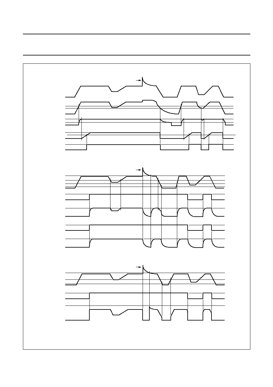
handbook, full pagewidth
load dump
load dump
VP
ignition 1
input
ignition 1
output
VP
ignition 2
input
ignition 2
output
7.0 V
4.5 V
3.25 V
-
100 V
5.0 V
50 V
1.1 V
2.2 V
-
100 V
5.0 V
50 V
2.0 V
Enable Schmitt trigger ignition 1
Enable Schmitt trigger ignition 2
VP
enable
regulator 3
enable
regulator 1
regulator 3
regulator 1
temperature
protection
150
∞
C
HOLD
>1.8 V
>1.3 V
LOW
HIGH
passive
active
>1.8 V
>1.3 V
MGR930
Fig.4 Timing diagram of ignition Schmitt triggers and HOLD.
1999 Sep 01
9
Philips Semiconductors
Preliminary specification
Multiple voltage regulator with switch and
ignition buffers
TDA3618JR
handbook, full pagewidth
VP
VBU
regulator 2
reset
delay
capacitor
reset
VP
enable
regulator 1
regulator 1
regulator 3
enable
regulator 3
VP
enable
power
switch
power
switch
output
6.5 V
5.4 V
5.0 V
1.9 V
0 V
5.0 V
0 V
18 V
10.4 V
7.0 V
4.0 V
2.2 V
10 V
0 V
load dump
5.0 V
0 V
16.9 V
7.0 V
4.0 V
16 V
0 V
3.0 V
6.0 V
2.0 V
2.2 V
2.0 V
2.2 V
2.0 V
load dump
load dump
MGK610
Power switch behaviour
VP and enable Schmitt trigger
Back-up Schmitt trigger and reset behaviour
Fig.5 Timing diagram of regulators and power switch.

1999 Sep 01
10
Philips Semiconductors
Preliminary specification
Multiple voltage regulator with switch and
ignition buffers
TDA3618JR
LIMITING VALUES
In accordance with the Absolute Maximum Rating System (IEC 134).
THERMAL CHARACTERISTICS
SYMBOL
PARAMETER
CONDITIONS
MIN.
MAX.
UNIT
V
P
supply voltage
operating
-
18
V
reverse polarity
non-operating
-
18
V
jump start
t
10 minutes
-
30
V
load dump protection
t
50 ms; t
r
2.5 ms
-
50
V
P
tot
total power dissipation
-
62
W
T
stg
storage temperature
non-operating
-
55
+150
∞
C
T
amb
ambient temperature
operating
-
40
+85
∞
C
T
j
junction temperature
operating
-
40
+150
∞
C
SYMBOL
PARAMETER
CONDITIONS
VALUE
UNIT
R
th(j-c)
thermal resistance from junction to case
2
K/W
R
th(j-a)
thermal resistance from junction to ambient
in free air
50
K/W
1999 Sep 01
11
Philips Semiconductors
Preliminary specification
Multiple voltage regulator with switch and
ignition buffers
TDA3618JR
CHARACTERISTICS
V
P
= 14.4 V; T
amb
= 25
∞
C; see Fig.8; unless otherwise specified.
SYMBOL
PARAMETER
CONDITIONS
MIN.
TYP.
MAX.
UNIT
Supplies
V
P
supply voltage
operating
11
14.4
18
V
regulator 2 on
note 1
2.4
14.4
18
V
jump start
t
10 minutes
-
-
30
V
load dump protection
t
50 ms; t
r
2.5 ms
-
-
50
V
I
q
quiescent supply current
V
P
= 12.4 V; note 2;
I
REG2
= 0.1 mA
-
310
400
µ
A
V
P
= 14.4 V; note 2;
I
REG2
= 0.1 mA
-
315
-
µ
A
Schmitt trigger for power supply of switch, regulators 1 and 3
V
thr
rising threshold voltage
6.5
7.0
7.5
V
V
thf
falling threshold voltage
4.0
4.5
5.0
V
V
hys
hysteresis voltage
-
2.5
-
V
Schmitt trigger for regulator 2
V
thr
rising threshold voltage
6.0
6.5
7.1
V
V
thf
falling threshold voltage
1.7
1.9
2.3
V
V
hys
hysteresis voltage
-
4.6
-
V
Schmitt trigger for enable input (regulators 1, 3 and switch)
V
thr
rising threshold voltage
1.4
1.8
2.4
V
V
thf
falling threshold voltage
0.9
1.3
1.9
V
V
hys
hysteresis voltage
I
REG
= I
SW
= 1 mA
-
0.5
-
V
I
LI
input leakage current
V
en
= 5 V
1
5
10
µ
A
Reset trigger level of regulator 2
V
thr
rising threshold voltage
V
P
rising; I
REG1
= 50 mA;
note 3
4.5
V
REG2
-
0.15
V
REG2
-
0.1
V
Schmitt triggers for HOLD output
V
thr1
rising threshold voltage of
regulator 1
V
P
rising; note 3
-
V
REG1
-
0.15
V
REG1
-
0.075
V
V
thf1
falling threshold voltage of
regulator 1
V
P
falling; note 3
8.1
V
REG1
-
0.35
-
V
V
hys1
hysteresis voltage due to
regulator 1
-
0.2
-
V
V
thr3
rising threshold voltage of
regulator 3
V
P
rising; note 3
-
V
REG3
-
0.15
V
REG3
-
0.075
V
V
thf3
falling threshold voltage of
regulator 3
V
P
falling; note 3
4.1
V
REG3
-
0.35
-
V
V
hys3
hysteresis voltage due to
regulator 3
-
0.2
-
V
1999 Sep 01
12
Philips Semiconductors
Preliminary specification
Multiple voltage regulator with switch and
ignition buffers
TDA3618JR
V
thr(VP)
rising threshold voltage of
supply voltage
V
en
= 0 V
9.1
9.7
10.3
V
V
thf(VP)
falling threshold voltage of
supply voltage
V
en
= 0 V
9.0
9.4
9.8
V
V
hys
hysteresis voltage of
supply voltage
V
en
= 0 V
-
0.3
-
V
Reset and hold buffer
I
sinkL
LOW-level sink current
V
RES/HOLD
0.8 V
2
-
-
mA
I
LO
output leakage current
V
P
= 14.4 V;
V
RES/HOLD
= 5 V
-
0.1
5
µ
A
t
r
rise time
note 4
-
7
50
µ
s
t
f
fall time
note 4
-
1
50
µ
s
Reset delay
I
ch
charge current
2
4
8
µ
A
I
dch
discharge current
500
800
-
µ
A
V
thr(RES)
rising voltage threshold
reset signal
2.5
3.0
3.5
V
t
d(RES)
delay time reset signal
C = 47 nF; note 5
20
35
70
ms
V
thr(SW)
rising voltage threshold
switch foldback protection
-
V
REG2
-
V
t
d(SW)
delay time switch foldback
protection
C = 47 nF; note 6
8
17.6
40
ms
Regulator 1 (I
REG1
= 5 mA; unless otherwise specified)
V
O(off)
output voltage off
-
1
400
mV
V
O(REG1)
output voltage
1 mA
I
REG1
600 mA
8.5
9.0
9.5
V
12 V
V
P
18 V
8.5
9.0
9.5
V
V
line regulation
12 V
V
P
18 V
-
2
75
mV
V
L
load regulation
1 mA
I
REG1
600 mA
-
20
100
mV
I
q
quiescent current
I
R1
= 600 mA
-
25
60
mA
SVRR
supply voltage ripple
rejection
f
i
= 3 kHz; V
i(p-p)
= 2 V
60
70
-
dB
V
d
drop-out voltage
I
REG1
= 550 mA;
V
P
= 9.5 V; note 7
-
0.4
0.7
V
I
REG1m
current limit
V
REG1
> 8.5 V; note 8
0.65
1.2
-
A
I
REG1sc
short-circuit current
R
L
0.5
; note 9
250
800
-
mA
Regulator 2 (I
REG2
= 5 mA; unless otherwise specified)
V
O(REG2)
output voltage
0.5 mA
I
REG2
300 mA
4.75
5.0
5.25
V
8 V
V
P
18 V
4.75
5.0
5.25
V
18 V
V
P
50 V;
I
REG2
150 mA
4.75
5.0
5.25
V
V
line regulation
6 V
V
P
18 V
-
2
50
mV
6 V
V
P
50 V
-
15
75
mV
SYMBOL
PARAMETER
CONDITIONS
MIN.
TYP.
MAX.
UNIT

1999 Sep 01
13
Philips Semiconductors
Preliminary specification
Multiple voltage regulator with switch and
ignition buffers
TDA3618JR
V
L
load regulation
1 mA
I
REG2
150 mA
-
20
50
mV
1 mA
I
REG2
300 mA
-
-
100
mV
SVRR
supply voltage ripple
rejection
f = 3 kHz; V
i(p-p)
= 2 V
60
70
-
dB
V
d
drop-out voltage
I
REG2
= 100 mA;
V
P
= 4.75 V; note 7
-
0.4
0.6
V
I
REG2
= 200 mA;
V
P
= 5.75 V; note 7
-
0.8
1.2
V
I
REG2
= 100 mA;
V
bu
= 4.75 V; note 10
-
0.2
0.5
V
I
REG2
= 200 mA;
V
bu
= 5.75 V; note 10
-
0.8
1.0
V
I
REG2m
current limit
V
REG2
> 4.5 V; note 8
0.32
0.37
-
A
I
REG2sc
short-circuit current
R
L
0.5
; note 9
20
100
-
mA
Regulator 3 (I
REG3
= 5 mA; unless otherwise specified)
V
O(off)
output voltage off
-
1
400
mV
V
O(REG3)
output voltage
1 mA
I
REG3
750 mA
4.75
5.0
5.25
V
7 V
V
P
18 V
4.75
5.0
5.25
V
V
line regulation
7 V
V
P
18 V
-
2
50
mV
V
L
load regulation
1 mA
I
REG3
750 mA
-
20
100
mV
I
q
quiescent current
I
R3
= 750 mA
-
19
45
mA
SVRR
supply voltage ripple
rejection
f
i
= 3 kHz; V
i(p-p)
= 2 V
60
70
-
dB
V
d
drop-out voltage
I
REG3
= 500 mA;
V
P
= 5.75 V; note 7
-
1
1.5
V
I
REG3m
current limit
V
REG3
> 4.5 V; note 8
0.80
0.90
-
A
I
REG3sc
short-circuit current
R
L
0.5
; note 9
100
400
-
mA
Power switch
V
d
drop-out voltage
I
SW
= 1 A; V
P
= 13.5 V;
note 11
-
0.45
0.70
V
I
SW
= 1.8 A; V
P
= 13.5 V;
note 11
-
1.0
1.8
V
I
dc
continuous current
V
P
= 16 V; V
SW
= 13.5 V
1.8
2.0
-
A
V
clamp
clamping voltage
V
P
17 V
13.5
15.0
16.0
V
I
M
peak current
V
P
= 17 V; notes 6, 12, 13
3
-
-
A
V
fb
fly back voltage behaviour I
SW
=
-
100 mA
-
V
P
+ 3
22
V
I
sc
short-circuit current
V
P
= 14.4 V; V
SW
< 1.2 V;
note 13
-
0.8
-
A
SYMBOL
PARAMETER
CONDITIONS
MIN.
TYP.
MAX.
UNIT

1999 Sep 01
14
Philips Semiconductors
Preliminary specification
Multiple voltage regulator with switch and
ignition buffers
TDA3618JR
backup switch
I
dc
continuous current
0.3
0.35
-
A
V
clamp
clamping voltage
V
P
16.7 V
-
-
16
V
I
r
reverse current
V
P
= 0 V; V
bu
= 12.4 V
-
-
900
µ
A
Schmitt trigger for enable input of ignition 1
V
thr
rising threshold voltage of
ignition 1 input
2.75
3.25
3.75
V
V
thf
falling threshold voltage of
ignition 1 input
0.8
-
1.3
V
V
hys
hysteresis voltage
1.5
-
-
V
I
LI
input leakage current
V
IGN1IN
= 5 V
-
-
1.0
µ
A
I
I(clamp)
input clamping current
V
IGN1IN
> 50 V
-
-
50
mA
V
IH(clamp)
HIGH-level input clamping
voltage
V
P
-
50
V
V
IL(clamp)
LOW-level input clamping
voltage
-
0.6
-
0
V
Schmitt trigger for power supply of ignition 1
V
thr
rising threshold voltage
6.5
7.0
7.5
V
V
thf
falling threshold voltage
note 14
4.0
4.5
5.0
V
Ignition 1 buffer
V
OL
LOW-level output voltage
I
IGN1OUT
= 0 mA
0
0.2
0.8
V
I
OL
LOW-level output current
V
IGN1OUT
0.8 V
0.45
0.8
-
mA
I
LO
output leakage current
V
IGN1OUT
= 5 V;
V
IGN1IN
= 0 V
-
-
1.0
µ
A
t
PLH
LOW-to-HIGH
propagation time
V
IGN1IN
rising from
0.8 to 3.75 V
-
-
500
µ
s
t
PHL
HIGH-to-LOW
propagation time
V
IGN1IN
falling from
3.75 to 0.8 V
-
-
500
µ
s
Schmitt trigger for enable input of ignition 2
V
thr
rising threshold voltage of
ignition 2 input
V
P
> 3.5 V
1.9
2.2
2.5
V
V
thf
falling threshold voltage of
ignition 2 input
V
P
> 3.5 V
1.7
2.0
2.3
V
V
hys
hysteresis voltage
V
P
> 3.5 V
0.1
0.2
0.5
V
I
LI
input leakage current
V
IGN2IN
= 5 V
-
-
1.0
µ
A
I
I(clamp)
input clamp current
V
IGN2IN
> 50 V
-
-
50
mA
V
IH(clamp)
HIGH-level input clamping
voltage
V
P
-
50
V
V
IL(clamp)
LOW-level input clamping
voltage
-
0.6
-
0
V
SYMBOL
PARAMETER
CONDITIONS
MIN.
TYP.
MAX.
UNIT
1999 Sep 01
15
Philips Semiconductors
Preliminary specification
Multiple voltage regulator with switch and
ignition buffers
TDA3618JR
Notes
1. Minimum operating voltage, only if V
P
has exceeded 6.5 V.
2. The quiescent current is measured in the standby mode. Therefore, the enable inputs of regulators 1, 3 and the
power switch are grounded and R
L(REG2)
=
(see Fig.8).
3. The voltage of the regulator drops as a result of a V
P
drop.
4. The rise and fall times are measured with a 10 k
pull-up resistor and a 50 pF load capacitor.
5. The delay time depends on the value of the capacitor:
6. The delay time depends on the value of the reset delay capacitor:
7. The drop-out voltage of regulators 1, 2 and 3 is measured between V
P
and REGn.
8. At current limit, I
REGmn
is held constant (see Fig.6 for the behaviour of I
REGmn
).
9. The foldback current protection limits the dissipated power at short circuit (see Fig.6).
10. The drop-out voltage measured between BU and REG2.
11. The drop-out voltage of the power switch is measured between V
P
and SW.
12. The maximum output current of the switch is limited to 1.8 A when the supply voltage exceeds 18 V. A test mode is
built in. The delay time of the switch is disabled when a voltage of V
P
+ 1 V is applied to the switch-enable input.
13. At short circuit, I
sc
of the power switch is held constant to a lower value than the continuous current after a delay of
at least 10 ms. A test-mode is built in. The delay time of the switch is disabled when a voltage of V
P
+ 1 V is applied
to the switch-enable input.
14. V
IGN1OUT
= LOW for V
IGN1OUT
> 1.2 V or V
EN1
> 1.3 V or V
EN3
> 1.3 V or V
ENSW
> 1.3 V.
Ignition 2 buffer
V
OL
LOW-level output voltage
I
IGN2OUT
= 0 mA
0
0.2
0.8
V
V
OH
HIGH-level output voltage
I
IGN2OUT
= 0 mA
4.5
5.0
5.25
V
I
OL
LOW-level output current
V
IGN2OUT
0.8 V
0.45
0.8
-
mA
I
OH
HIGH-level output current
V
IGN2OUT
4.5 V
-
0.45
-
2.0
-
mA
I
LO
output leakage current
(source)
V
IGN2OUT
= 5 V;
V
IGN2IN
= 0 V
-
-
1.0
µ
A
t
PLH
LOW-to-HIGH
propagation time
V
IGN2IN
rising from
1.7 to 2.5 V
-
-
500
µ
s
t
PHL
HIGH-to-LOW
propagation time
V
IGN2IN
falling from
2.5 to 1.7 V
-
-
500
µ
s
SYMBOL
PARAMETER
CONDITIONS
MIN.
TYP.
MAX.
UNIT
t
d
C
I
ch
------
V
C(th)
◊
C
750
10
3
◊
(
)
◊
s
[ ]
=
=
t
d_high current
C
I
ch
-------
V
C th
( )
◊
C
375
10
3
◊
(
)
◊
s
[ ]
=
=

1999 Sep 01
16
Philips Semiconductors
Preliminary specification
Multiple voltage regulator with switch and
ignition buffers
TDA3618JR
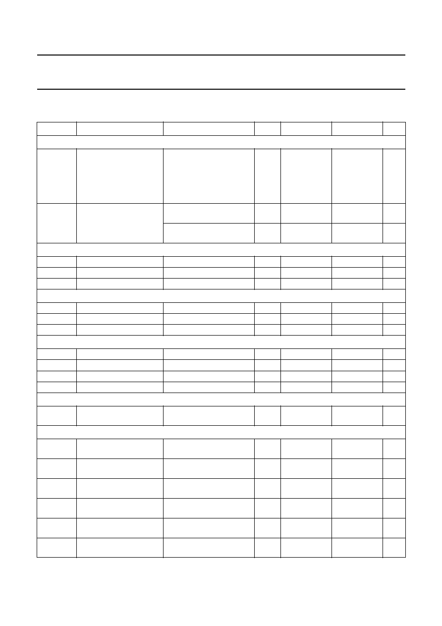
Fig.6 Foldback current protection of the regulators.
a. Regulator 1.
b. Regulator 2.
handbook, halfpage
MBK946
9 V
IREG1sc
IREG1
IREG1m
VO(REG1)
handbook, halfpage
MGL599
5.0 V
IREG3sc
IREG3
IREG3m
VO(REG3)
handbook, halfpage
MGL598
5.0 V
IREG2sc
IREG2
IREG2m
VO(REG2)
handbook, full pagewidth
>
1.8 A
>
3 A
1 A
generates
hold
MGR931
VP
-
3.3 V
2VBE
Isw
Vsw
not
delayed
delayed
Fig.7 Current protection of the power switch.
1999 Sep 01
17
Philips Semiconductors
Preliminary specification
Multiple voltage regulator with switch and
ignition buffers
TDA3618JR
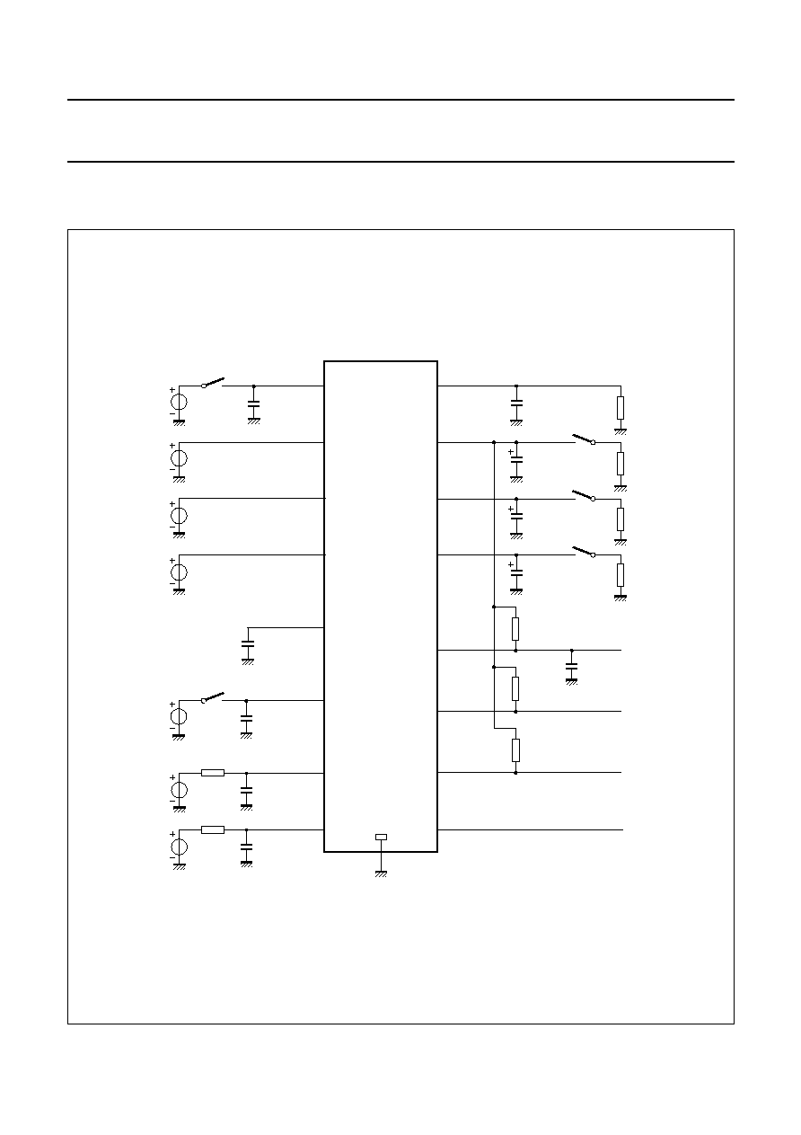
TEST AND APPLICATION INFORMATION
Test information
handbook, full pagewidth
MGR932
enable input regulator 3
reset delay
capacitor
reset
output
C3
10
µ
F
C2
220 nF
C1
220 nF
C4
10
µ
F
ignition 1
output
ignition 2
output
R2
10 k
RL(REG2)
5 k
RL(SW)
12 k
5 V
5 V
10 V
regulator 3
output
regulator 1
output
regulator 2
output
C5
10
µ
F
C6
1
µ
F
C7
47 nF
RL(REG1)
10 k
RL(REG3)
5 k
power switch output
17
15
2
7
8
hold
output
12
9
3
4
13
16
11
1
14
TDA3618JR
ground
VP
supply voltage
VENSW
VEN3
enable input regulator 1
enable input power switch
10
VEN1
back-up
ignition 2
input
10 k
R6
C10
1 nF
ignition 1
input
5
6
VIGN2
10 k
R5
C9
1 nF
VIGN1
C8
Vbu
R3
10 k
R4
10 k
Fig.8 Test circuit.

1999 Sep 01
18
Philips Semiconductors
Preliminary specification
Multiple voltage regulator with switch and
ignition buffers
TDA3618JR
Application information
N
OISE
Table 1
Noise figures
Note
1. Measured at a bandwidth of 200 kHz.
The noise on the supply line depends on the value of the
supply capacitor and is caused by a current noise (the
output noise of the regulators is translated to a current
noise by the output capacitors). When a high frequency
capacitor of 220 nF in parallel with an electrolytic capacitor
of 100
µ
F is connected directly to pins 1 and 14 (supply
and ground), the noise is minimal.
S
TABILITY
The regulators are stabilized with the externally connected
output capacitors.
The output capacitors can be selected by using the graphs
of Figs 9 and 10. When an electrolytic capacitor is used,
the temperature behaviour of this output capacitor can
cause oscillations at a low temperature. The two examples
below show how an output capacitor value is selected.
Example 1
Regulators 1 and 3 are stabilized with an electrolytic
output capacitor of 220
µ
F (ESR = 0.15
). At
-
30
∞
C, the
capacitor value is decreased to 73
µ
F and the ESR is
increased to 1.1
. The regulator remains stable at
-
30
∞
C.
Example 2
Regulator 2 is stabilized with a 10
µ
F electrolytic capacitor
(ESR = 3
). At
-
30
∞
C, the capacitor value is decreased
to 3
µ
F and the ESR is increased to 23.1
. Using Fig.10,
the regulator will be instable at
-
30
∞
C.
Solution
To avoid problems with stability at low temperatures, the
use of tantalum capacitors is recommended. Use a
tantalum capacitor of 10
µ
F or a larger electrolytic
capacitor.
REGULATOR
NOISE FIGURE (
µ
V)
(1)
C
o
= 10
µ
F
C
o
= 47
µ
F
C
o
= 100
µ
F
1
tbf
150
tbf
2
tbf
150
tbf
3
tbf
200
tbf
Fig.9
Curve for selecting the value of output
capacitor for regulators 1 and 3.
handbook, halfpage
0
0.1
1
10
C (
µ
F)
MGK612
stable region
maximum ESR
100
R
(
)
20
15
10
5
Fig.10 Curve for selecting the value of output
capacitor for regulator 2.
handbook, halfpage
2
0
0.22
1
10
C (
µ
F)
MGK613
4
6
8
10
12
stable region
maximum ESR
minimum ESR
100
R
(
)
14
1999 Sep 01
19
Philips Semiconductors
Preliminary specification
Multiple voltage regulator with switch and
ignition buffers
TDA3618JR
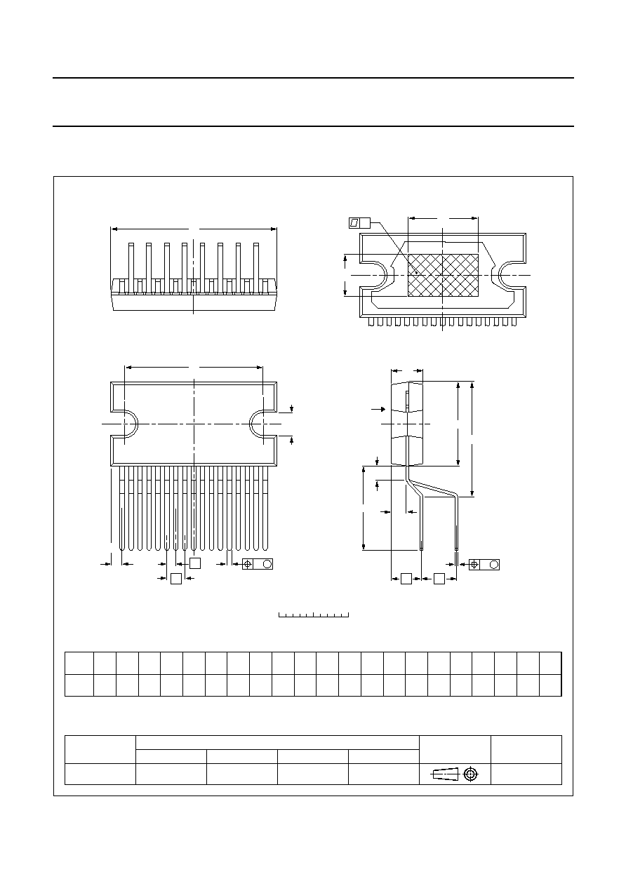
PACKAGE OUTLINE
REFERENCES
OUTLINE
VERSION
EUROPEAN
PROJECTION
ISSUE DATE
97-05-20
IEC
JEDEC
EIAJ
DIMENSIONS (mm are the original dimensions)
Note
1. Plastic or metal protrusions of 0.25 mm maximum per side are not included.
SOT475-1
0
5
10 mm
scale
D
L
E
A
c
A
2
L
3
Q
w
M
b
p
1
d
D
Z
e
e
x
h
1
17
j
Eh
non-concave
DBS17P: plastic DIL-bent-SIL (special bent) power package; 17 leads (lead length 12 mm)
SOT475-1
view B: mounting base side
m
2
e
v
M
B
UNIT
A
e
1
A
2
b
p
c
D
(1)
E
(1)
Z
(1)
d
e
D
h
L
L
3
m
mm
17.0
15.5
4.6
4.2
0.75
0.60
0.48
0.38
24.0
23.6
20.0
19.6
10
2.54
v
0.8
12.2
11.8
1.27
e
2
5.08
2.4
1.6
E
h
6
2.00
1.45
2.1
1.8
3.4
3.1
4.3
12.4
11.0
Q
j
0.4
w
0.03
x
1999 Sep 01
20
Philips Semiconductors
Preliminary specification
Multiple voltage regulator with switch and
ignition buffers
TDA3618JR
SOLDERING
Introduction to soldering through-hole mount
packages
This text gives a brief insight to wave, dip and manual
soldering. A more in-depth account of soldering ICs can be
found in our
"Data Handbook IC26; Integrated Circuit
Packages" (document order number 9398 652 90011).
Wave soldering is the preferred method for mounting of
through-hole mount IC packages on a printed-circuit
board.
Soldering by dipping or by solder wave
The maximum permissible temperature of the solder is
260
∞
C; solder at this temperature must not be in contact
with the joints for more than 5 seconds.
The total contact time of successive solder waves must not
exceed 5 seconds.
The device may be mounted up to the seating plane, but
the temperature of the plastic body must not exceed the
specified maximum storage temperature (T
stg(max)
). If the
printed-circuit board has been pre-heated, forced cooling
may be necessary immediately after soldering to keep the
temperature within the permissible limit.
Manual soldering
Apply the soldering iron (24 V or less) to the lead(s) of the
package, either below the seating plane or not more than
2 mm above it. If the temperature of the soldering iron bit
is less than 300
∞
C it may remain in contact for up to
10 seconds. If the bit temperature is between
300 and 400
∞
C, contact may be up to 5 seconds.
Suitability of through-hole mount IC packages for dipping and wave soldering methods
Note
1. For SDIP packages, the longitudinal axis must be parallel to the transport direction of the printed-circuit board.
DEFINITIONS
LIFE SUPPORT APPLICATIONS
These products are not designed for use in life support appliances, devices, or systems where malfunction of these
products can reasonably be expected to result in personal injury. Philips customers using or selling these products for
use in such applications do so at their own risk and agree to fully indemnify Philips for any damages resulting from such
improper use or sale.
PACKAGE
SOLDERING METHOD
DIPPING
WAVE
DBS, DIP, HDIP, SDIP, SIL
suitable
suitable
(1)
Data sheet status
Objective specification
This data sheet contains target or goal specifications for product development.
Preliminary specification
This data sheet contains preliminary data; supplementary data may be published later.
Product specification
This data sheet contains final product specifications.
Limiting values
Limiting values given are in accordance with the Absolute Maximum Rating System (IEC 134). Stress above one or
more of the limiting values may cause permanent damage to the device. These are stress ratings only and operation
of the device at these or at any other conditions above those given in the Characteristics sections of the specification
is not implied. Exposure to limiting values for extended periods may affect device reliability.
Application information
Where application information is given, it is advisory and does not form part of the specification.

1999 Sep 01
21
Philips Semiconductors
Preliminary specification
Multiple voltage regulator with switch and
ignition buffers
TDA3618JR
NOTES

1999 Sep 01
22
Philips Semiconductors
Preliminary specification
Multiple voltage regulator with switch and
ignition buffers
TDA3618JR
NOTES

1999 Sep 01
23
Philips Semiconductors
Preliminary specification
Multiple voltage regulator with switch and
ignition buffers
TDA3618JR
NOTES

© Philips Electronics N.V.
SCA
All rights are reserved. Reproduction in whole or in part is prohibited without the prior written consent of the copyright owner.
The information presented in this document does not form part of any quotation or contract, is believed to be accurate and reliable and may be changed
without notice. No liability will be accepted by the publisher for any consequence of its use. Publication thereof does not convey nor imply any license
under patent- or other industrial or intellectual property rights.
Internet: http://www.semiconductors.philips.com
1999
67
Philips Semiconductors ≠ a worldwide company
For all other countries apply to: Philips Semiconductors,
International Marketing & Sales Communications, Building BE-p, P.O. Box 218,
5600 MD EINDHOVEN, The Netherlands, Fax. +31 40 27 24825
Argentina: see South America
Australia: 3 Figtree Drive, HOMEBUSH, NSW 2140,
Tel. +61 2 9704 8141, Fax. +61 2 9704 8139
Austria: Computerstr. 6, A-1101 WIEN, P.O. Box 213,
Tel. +43 1 60 101 1248, Fax. +43 1 60 101 1210
Belarus: Hotel Minsk Business Center, Bld. 3, r. 1211, Volodarski Str. 6,
220050 MINSK, Tel. +375 172 20 0733, Fax. +375 172 20 0773
Belgium: see The Netherlands
Brazil: see South America
Bulgaria: Philips Bulgaria Ltd., Energoproject, 15th floor,
51 James Bourchier Blvd., 1407 SOFIA,
Tel. +359 2 68 9211, Fax. +359 2 68 9102
Canada: PHILIPS SEMICONDUCTORS/COMPONENTS,
Tel. +1 800 234 7381, Fax. +1 800 943 0087
China/Hong Kong: 501 Hong Kong Industrial Technology Centre,
72 Tat Chee Avenue, Kowloon Tong, HONG KONG,
Tel. +852 2319 7888, Fax. +852 2319 7700
Colombia: see South America
Czech Republic: see Austria
Denmark: Sydhavnsgade 23, 1780 COPENHAGEN V,
Tel. +45 33 29 3333, Fax. +45 33 29 3905
Finland: Sinikalliontie 3, FIN-02630 ESPOO,
Tel. +358 9 615 800, Fax. +358 9 6158 0920
France: 51 Rue Carnot, BP317, 92156 SURESNES Cedex,
Tel. +33 1 4099 6161, Fax. +33 1 4099 6427
Germany: Hammerbrookstraþe 69, D-20097 HAMBURG,
Tel. +49 40 2353 60, Fax. +49 40 2353 6300
Hungary: see Austria
India: Philips INDIA Ltd, Band Box Building, 2nd floor,
254-D, Dr. Annie Besant Road, Worli, MUMBAI 400 025,
Tel. +91 22 493 8541, Fax. +91 22 493 0966
Indonesia: PT Philips Development Corporation, Semiconductors Division,
Gedung Philips, Jl. Buncit Raya Kav.99-100, JAKARTA 12510,
Tel. +62 21 794 0040 ext. 2501, Fax. +62 21 794 0080
Ireland: Newstead, Clonskeagh, DUBLIN 14,
Tel. +353 1 7640 000, Fax. +353 1 7640 200
Israel: RAPAC Electronics, 7 Kehilat Saloniki St, PO Box 18053,
TEL AVIV 61180, Tel. +972 3 645 0444, Fax. +972 3 649 1007
Italy: PHILIPS SEMICONDUCTORS, Via Casati, 23 - 20052 MONZA (MI),
Tel. +39 039 203 6838, Fax +39 039 203 6800
Japan: Philips Bldg 13-37, Kohnan 2-chome, Minato-ku,
TOKYO 108-8507, Tel. +81 3 3740 5130, Fax. +81 3 3740 5057
Korea: Philips House, 260-199 Itaewon-dong, Yongsan-ku, SEOUL,
Tel. +82 2 709 1412, Fax. +82 2 709 1415
Malaysia: No. 76 Jalan Universiti, 46200 PETALING JAYA, SELANGOR,
Tel. +60 3 750 5214, Fax. +60 3 757 4880
Mexico: 5900 Gateway East, Suite 200, EL PASO, TEXAS 79905,
Tel. +9-5 800 234 7381, Fax +9-5 800 943 0087
Middle East: see Italy
Netherlands: Postbus 90050, 5600 PB EINDHOVEN, Bldg. VB,
Tel. +31 40 27 82785, Fax. +31 40 27 88399
New Zealand: 2 Wagener Place, C.P.O. Box 1041, AUCKLAND,
Tel. +64 9 849 4160, Fax. +64 9 849 7811
Norway: Box 1, Manglerud 0612, OSLO,
Tel. +47 22 74 8000, Fax. +47 22 74 8341
Pakistan: see Singapore
Philippines: Philips Semiconductors Philippines Inc.,
106 Valero St. Salcedo Village, P.O. Box 2108 MCC, MAKATI,
Metro MANILA, Tel. +63 2 816 6380, Fax. +63 2 817 3474
Poland: Ul. Lukiska 10, PL 04-123 WARSZAWA,
Tel. +48 22 612 2831, Fax. +48 22 612 2327
Portugal: see Spain
Romania: see Italy
Russia: Philips Russia, Ul. Usatcheva 35A, 119048 MOSCOW,
Tel. +7 095 755 6918, Fax. +7 095 755 6919
Singapore: Lorong 1, Toa Payoh, SINGAPORE 319762,
Tel. +65 350 2538, Fax. +65 251 6500
Slovakia: see Austria
Slovenia: see Italy
South Africa: S.A. PHILIPS Pty Ltd., 195-215 Main Road Martindale,
2092 JOHANNESBURG, P.O. Box 58088 Newville 2114,
Tel. +27 11 471 5401, Fax. +27 11 471 5398
South America: Al. Vicente Pinzon, 173, 6th floor,
04547-130 S√O PAULO, SP, Brazil,
Tel. +55 11 821 2333, Fax. +55 11 821 2382
Spain: Balmes 22, 08007 BARCELONA,
Tel. +34 93 301 6312, Fax. +34 93 301 4107
Sweden: Kottbygatan 7, Akalla, S-16485 STOCKHOLM,
Tel. +46 8 5985 2000, Fax. +46 8 5985 2745
Switzerland: Allmendstrasse 140, CH-8027 ZÐRICH,
Tel. +41 1 488 2741 Fax. +41 1 488 3263
Taiwan: Philips Semiconductors, 6F, No. 96, Chien Kuo N. Rd., Sec. 1,
TAIPEI, Taiwan Tel. +886 2 2134 2886, Fax. +886 2 2134 2874
Thailand: PHILIPS ELECTRONICS (THAILAND) Ltd.,
209/2 Sanpavuth-Bangna Road Prakanong, BANGKOK 10260,
Tel. +66 2 745 4090, Fax. +66 2 398 0793
Turkey: Yukari Dudullu, Org. San. Blg., 2.Cad. Nr. 28 81260 Umraniye,
ISTANBUL, Tel. +90 216 522 1500, Fax. +90 216 522 1813
Ukraine: PHILIPS UKRAINE, 4 Patrice Lumumba str., Building B, Floor 7,
252042 KIEV, Tel. +380 44 264 2776, Fax. +380 44 268 0461
United Kingdom: Philips Semiconductors Ltd., 276 Bath Road, Hayes,
MIDDLESEX UB3 5BX, Tel. +44 208 730 5000, Fax. +44 208 754 8421
United States: 811 East Arques Avenue, SUNNYVALE, CA 94088-3409,
Tel. +1 800 234 7381, Fax. +1 800 943 0087
Uruguay: see South America
Vietnam: see Singapore
Yugoslavia: PHILIPS, Trg N. Pasica 5/v, 11000 BEOGRAD,
Tel. +381 11 62 5344, Fax.+381 11 63 5777
Printed in The Netherlands
545002/02/pp
24
Date of release:
1999 Sep 01
Document order number:
9397 750 06265