 | –≠–ª–µ–∫—Ç—Ä–æ–Ω–Ω—ã–π –∫–æ–º–ø–æ–Ω–µ–Ω—Ç: TDA4655 | –°–∫–∞—á–∞—Ç—å:  PDF PDF  ZIP ZIP |
Document Outline
- FEATURES
- GENERAL DESCRIPTION
- QUICK REFERENCE DATA
- ORDERING INFORMATION
- PINNING
- FUNCTIONAL DESCRIPTION
- ACC-stage
- Reference signal generation
- Demodulation
- Blanking, colour-killer, buffers
- Identification and system control
- Sandcastle detector and pulse processing
- Bandgap reference
- LIMITING VALUES
- THERMAL RESISTANCE
- CHARACTERISTICS
- QUALITY SPECIFICATION
- PACKAGE OUTLINES
- SOLDERING
- DEFINITIONS
- LIFE SUPPORT APPLICATIONS

DATA SHEET
Preliminary specification
File under Integrated Circuits, IC02
June 1993
INTEGRATED CIRCUITS
TDA4655
Generic multi-standard decoder

June 1993
2
Philips Semiconductors
Preliminary specification
Generic multi-standard decoder
TDA4655
FEATURES
∑
Low voltage (8 V)
∑
Low power dissipation (250 mW)
∑
Automatic standard recognition
∑
No adjustments required
∑
Reduced external components
∑
Not all time constants integrated (ACC, SECAM
de-emphasis).
GENERAL DESCRIPTION
The TDA4655 is a monolithic integrated multi-standard
colour decoder for PAL, SECAM and NTSC (3.58 and
4.43 MHz) with negative colour difference output signals.
It is adapted to the integrated baseband delay line
TDA4660/61.
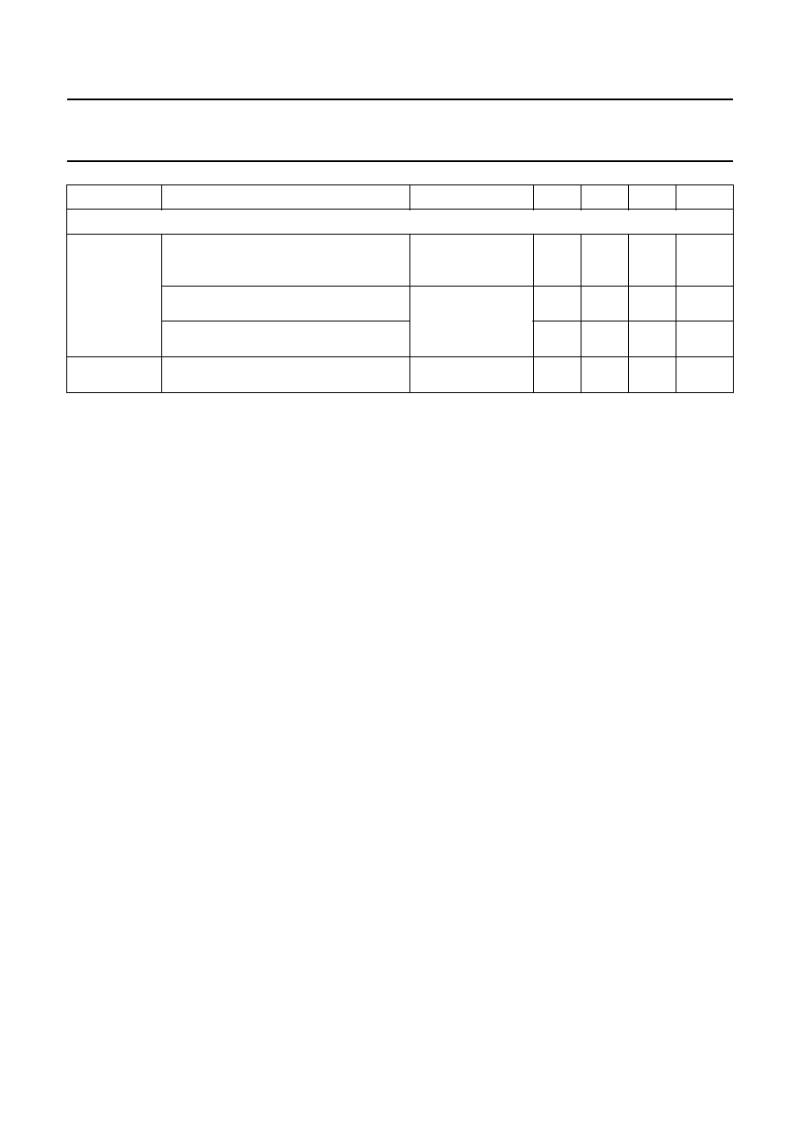
QUICK REFERENCE DATA
Notes to quick reference data
1. Within 2 dB output voltage deviation.
2. Burstkey width for PAL 4.3
µ
s, for NTSC 3.6
µ
s.
Burst width for PAL and NTSC 2.25
µ
s ratio burst chrominance amplitude 1/2.2.
ORDERING INFORMATION
Note
1. SOT234-1; 1996 November 26.
2. SOT137-1; 1996 November 26.
SYMBOL
PARAMETER
CONDITIONS
MIN.
TYP.
MAX.
UNIT
Supply
V
P
supply voltage
7.2
8.0
8.8
V
I
P
supply current
V
P
= 8.0 V; without load 25
31
37
mA
P
tot
total power dissipation
V
P
= 8.0 V; without load
-
248
296
mW
Inputs
V
11
chrominance input voltage (peak-to-peak value) note 1
20
200
400
mV
V
24
sandcastle input voltage
-
-
13.2
V
Outputs
V1
colour difference output signals
(peak-to-peak value)
independent of supply voltage; note 2
-
(R
-
Y) output PAL and NTSC 4.43 MHz
442
525
624
mV
NTSC 3.58 MHz
370
440
523
mV
SECAM
950
1050
1150
mV
V
3
-
(B-Y) output PAL and NTSC 4.43 MHz
559
665
791
mV
NTSC 3.58 MHz
468
557
662
mV
SECAM
1200 1330
1460
mV
EXTENDED
TYPE NUMBER
PACKAGE
PINS
PIN POSITION
MATERIAL
CODE
TDA4655
24
SDIL
plastic
SOT234
(1)
TDA4655T
24
SO
plastic
SOT137A
(2)
June 1993
3
Philips Semiconductors
Preliminary specification
Generic multi-standard decoder
TDA4655
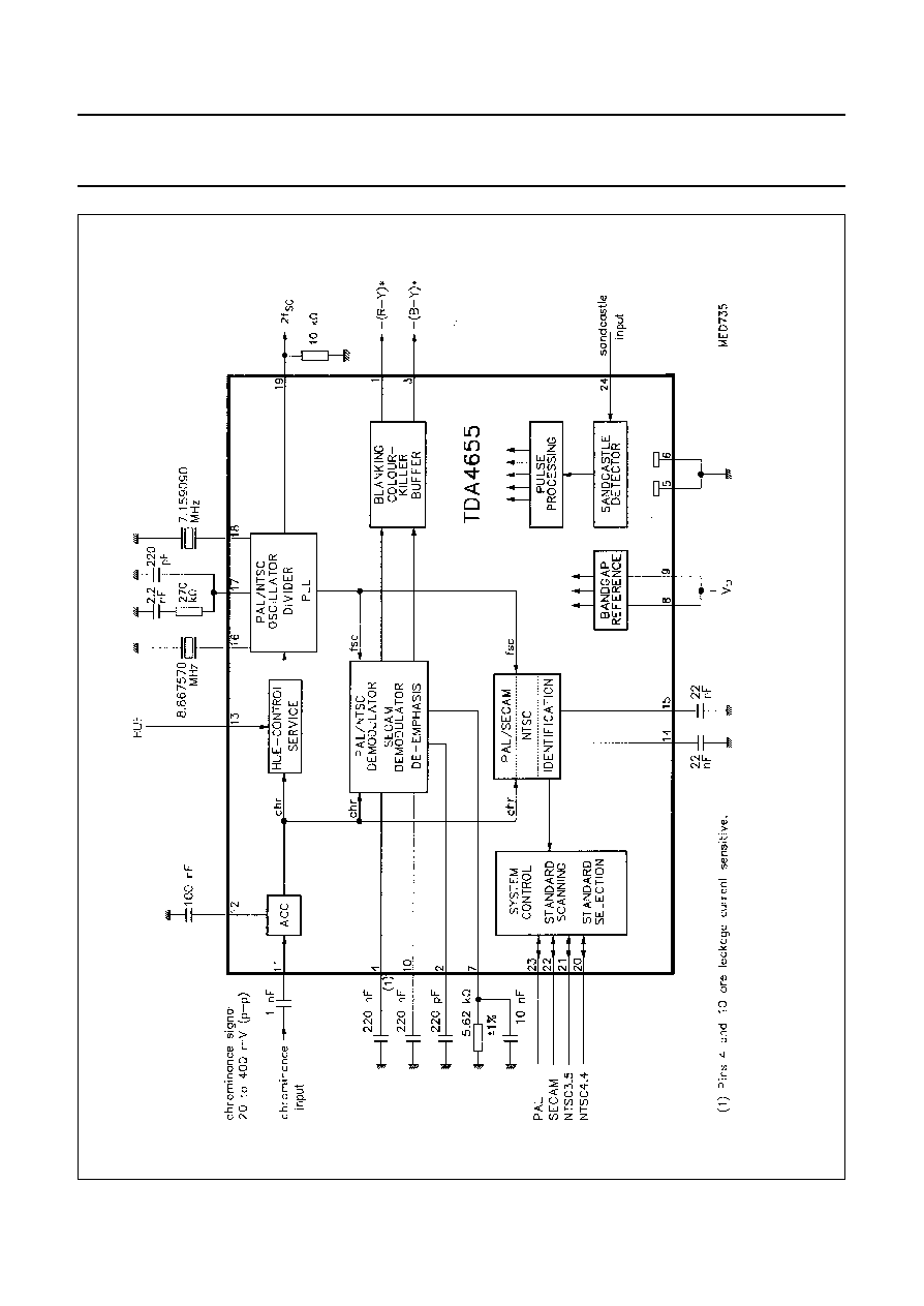
Fig.1 Block diagram.
June 1993
4
Philips Semiconductors
Preliminary specification
Generic multi-standard decoder
TDA4655
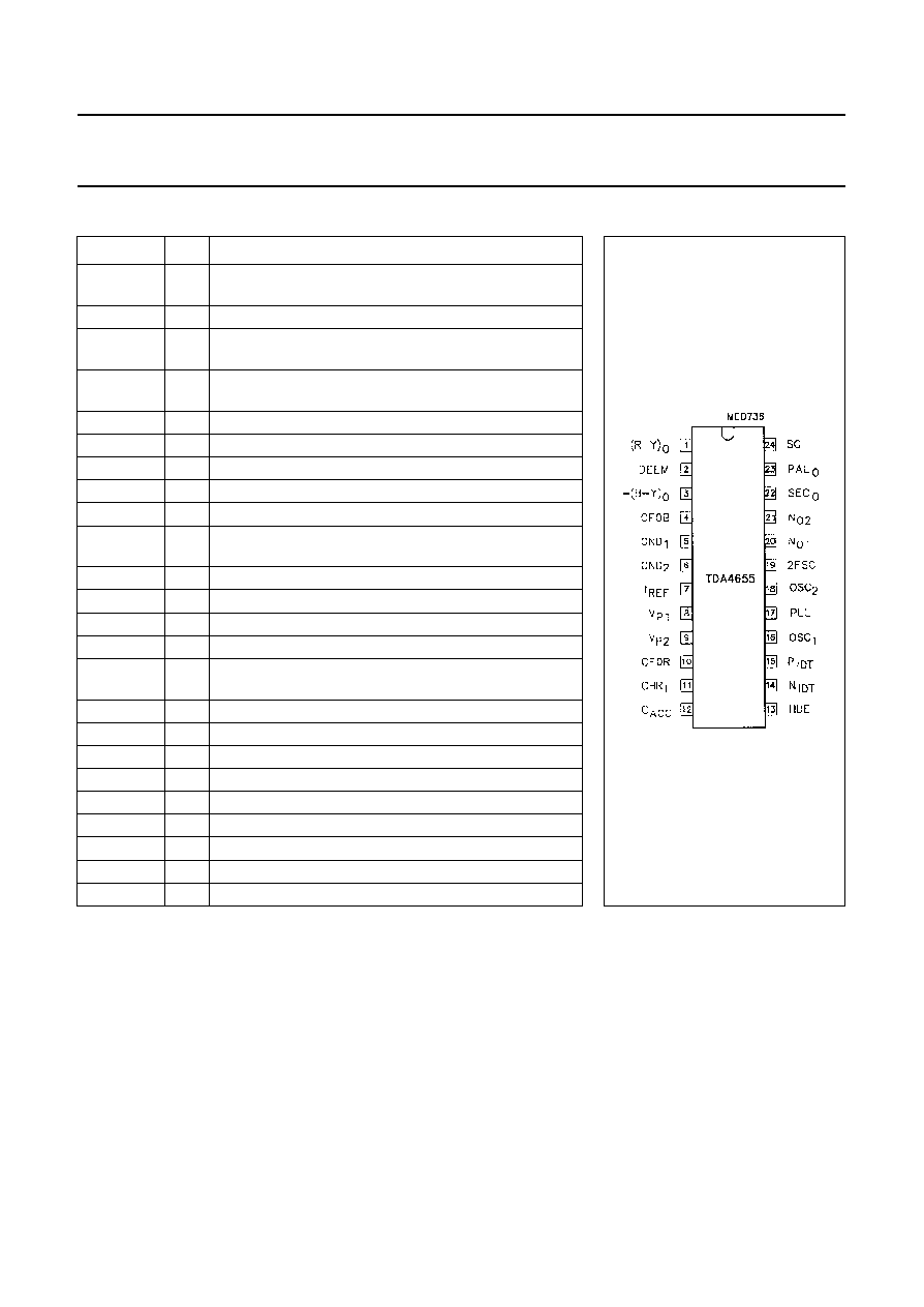
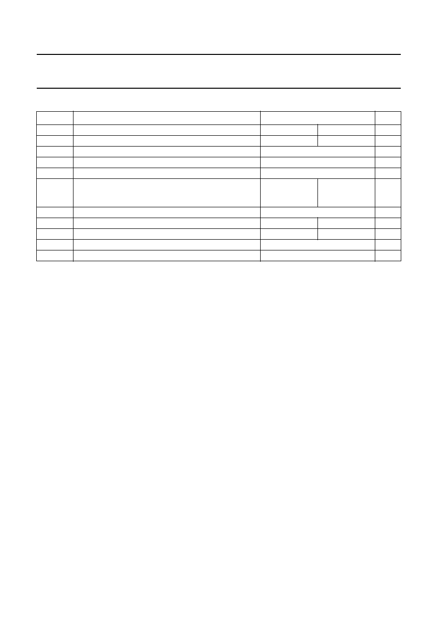
PINNING
SYMBOL
PIN
DESCRIPTION
-
(R
-
Y)o
1
colour difference signal output
-
(R
-
Y)* for baseband
delay line
DEEM
2
external capacitor for SECAM de-emphasis
-
(B
-
Y)o
3
colour difference signal output
-
(B
-
Y)* for baseband
delay line
CFOB
4
external capacitor SECAM demodulator control (B
-
Y)
Channel
GND
1
5
ground
GND
2
6
ground
I
REF
7
external resistor for SECAM oscillator
V
P1
8
supply 8 V
V
P2
9
supply 8 V
CFOR
10
external capacitor SECAM demodulator control (R
-
Y)
Channel
CHR
I
11
chrominance signal input
C
ACC
12
external capacitor for ACC control
HUE
13
input for HUE control and service switch
N
IDT
14
external capacitor for identification circuit (NTSC)
P
IDT
15
external capacitor for identification circuit (PAL and
SECAM)
OSC
1
16
PAL crystal
PLL
17
external loop filter
OSC
2
18
NTSC crystal
2FSC
19
2
◊
f
SC
output
N
O1
20
standard setting input/output for NTSC 4.43
N
O2
21
standard setting input/output for NTSC 3.58
SEC
O
22
standard setting input/output for SECAM
PAL
O
23
standard setting input/output for PAL
SC
24
sandcastle input
Fig.2 Pin configuration.

June 1993
5
Philips Semiconductors
Preliminary specification
Generic multi-standard decoder
TDA4655
FUNCTIONAL DESCRIPTION
The IC contains all functions required
for the identification and
demodulation of signals with the
standards PAL, SECAM, NTSC 3.5
with 3.58 MHz colour-carrier
frequency and NTSC 4.3 with
4.43 MHz colour-carrier frequency.
When an unknown signal is fed into
the input, the circuit has to detect the
standard of the signal, and has to
switch on successively the
appropriate input filter, crystal (8.8 or
7.2 MHz) and demodulator and
finally, after having identified the
signal, it has to switch on the colour
and, in event of NTSC reception, the
hue control. At the outputs the two
colour difference signals
-
(R
-
Y)* and
-(B
-
Y)* are available. The
identification circuit is able to
discriminate between NTSC signals
with colour-carrier frequencies of
3.58 MHz or 4.43 MHz.
ACC-stage
The chrominance signal is fed into the
asymmetrical input (pin 11) of the
ACC-stage (Automatic Colour
Control). The input has to be AC
coupled and has an input impedance
of 20 k
in parallel with 10 pF.
To control the chrominance amplitude
the modulation independent burst
amplitude is measured during the
burstkey pulse which is derived from
the sandcastle pulse present at pin
24. The generated error current is fed
into an external storage capacitor at
pin 12. The integrated error voltage
controls the gain of the ACC stage so
that its output is independent of input
signal variations.
The measurement is disabled during
the vertical blanking to avoid failures
because of missing burst signals.
Reference signal generation
The reference signal generation is
achieved by a PLL system. The
reference oscillator operates at twice
the colour-carrier frequency and is
locked on the burst of the
chrominance signal (chr). A divider
provides reference signals (f
SC
) with
the correct phase relationship for the
PAL/NTSC demodulator and the
identification part. In the SECAM
mode the two f
0
frequencies are
derived from the PAL crystal
frequency by special dividers. In this
mode the oscillator is not locked to
the input signal. In the NTSC mode
the hue control circuit is switched
between ACC stage and PLL. The
phase shift of the signal can be
controlled by a DC voltage at pin 13.
The hue control circuit is switched off
during scanning. The reference
frequency (2
◊
f
SC
) is available at pin
19 to drive a PAL comb filter for
example.
Demodulation
The demodulation of the colour signal
requires two demodulators. One is
common for PAL and NTSC signals,
the other is for SECAM signals.
The PAL/NTSC demodulator consists
of two synchronized demodulators,
one for the (B
-
Y) Channel and the
other for the (R
-
Y) Channel. The
required reference signals (f
SC
) are
input from the reference oscillator. In
NTSC mode the PAL switch is
disabled.
The SECAM demodulator consists of
a PLL system. During vertical
blanking the PLL oscillator is tuned to
the f
0
frequencies to provide a fixed
black level at the demodulator output.
During demodulation the control
voltages are stored in the external
capacitors at pins 4 and 10.
The oscillator requires an external
resistor at pin 7. Behind the PLL
demodulator the signal is fed into the
de-emphasis network which consists
of two internal resistors (2.8 k
and
5.6 k
) and an external capacitor
connected at pin 2 (220 pF).
After demodulation the signal is
filtered and then fed into the next
stage.
Blanking, colour-killer, buffers
As a result of using only one
demodulator in SECAM mode the
demodulated signal has to be split up
in the (B
-
Y) Channel and the (R
-
Y)
Channel. The unwanted signals
occuring every second line, (R
-
Y) in
the (B
-
Y) Channel and (B
-
Y) and in
the (R
-
Y) Channel, have to be
blanked. This happens in the blanking
stage by an artificial black level being
inserted alternately every second
line.
To avoid disturbances during line and
field flyback these parts of the colour
differential signals are blanked in all
modes.
When no signal has been identified,
the colour is switched off (signals are
blanked) by the colour killer. At the
end of the colour channels are
low-ohmic buffers (emitter followers).
The CD output signals
-
(B
-
Y)* and
-
(R
-
Y)* are available at pins 1 and 3.
Identification and system control
The identification part contains three
identification demodulators.
The first demodulates in PAL mode. It
is only active during the burstkey
pulse. The reference signal (f
SC
) has
the (R
-
Y) phase.
The second demodulator (PLL
system) operates in SECAM mode
and is active also during the burstkey
pulse, but delayed by 2
µ
s.
The PLL demodulator discriminates
the frequency difference between the
unmodulated f
0
frequencies of the
incoming signal (chr) and the
reference frequency input from the
crystal oscillator.
These two demodulators are followed
by an H/2 switch `rectifying' the

June 1993
6
Philips Semiconductors
Preliminary specification
Generic multi-standard decoder
TDA4655
demodulated signal. The result is an
identification signal (P
IDT,
pin 15) that
is positive for a PAL signal in PAL
mode, for a SECAM signal in SECAM
mode and for a PAL signal in
NTSC 4.4 mode.
If P
IDT
is positive in SECAM mode,
the scanner switches back to the PAL
mode in order to prevent a PAL signal
being erroneously identified as a
SECAM signal (PAL priority). If then
P
IDT
is not positive, the scanner
returns to SECAM mode and remains
there until P
IDT
is positive again. In
the event of a field frequency of 60 Hz
the signal can not be identified as a
SECAM signal, even if P
IDT
is
positive. In this event the scanner
switches forward in the NTSC 3.5
mode. If the H/2 signal has the wrong
polarity, the identification signal is
negative and the H/2 flip-flop is set to
the correct phase.
The third demodulator operates in
NTSC mode and is active during the
burstkey pulse. The resulting
identification signal (N
IDT
, pin 14) is
positive for PAL and NTSC 4.4
signals in NTSC 4.4 mode and for
NTSC 3.5 signals in the NTSC 3.5
mode. The reference signal has the
(B
-
Y) phase.
The two identification signals allow an
unequivocal identification of the
received signal. In the event of a
signal being identified, the scanning is
stopped and after a delay time the
colour is switched on.
The standard outputs (active HIGH)
are available at the pins 20, 21, 22
and 23. During scanning the HIGH
level is 2.5 V and when a signal has
been identified the HIGH level is
switched to 6 V. The standard pins
can also be used as inputs in order to
force the IC into a desired mode
(Forced Standard Setting).
Sandcastle detector and pulse
processing
In the sandcastle detector the super
sandcastle pulse (SC) present at pin
24 is compared with three internal
threshold levels by means of three
differential amplifiers. The derived
signals are the burstkey pulse, the
horizontal blanking pulse and the
combined horizontal and vertical
blanking pulse. These signals are
processed into various control pulses
required for the timing of the IC.
Bandgap reference
In order to ensure that the CD output
signals and the threshold levels of the
sandcastle detector are independent
of supply voltage variations a
bandgap reference voltage has been
integrated.
LIMITING VALUES
In accordance with the Absolute Maximum Rating System (IEC 134).
THERMAL RESISTANCE
SYMBOL
PARAMETER
CONDITIONS
MIN.
MAX.
UNIT
T
stg
storage temperature
-
25
+
150
∞
C
T
amb
operating ambient temperature
0
+
70
∞
C
V
p
supply voltage
-
8.8
V
P
tot
power dissipation
without load
-
330
mW
V
24
voltage at pin 24
I
max
= 10
µ
A
-
15
V
voltage at all other pins
I
max
= 100
µ
A
-
V
P
+
V
be
V
SYMBOL
PARAMETER
THERMAL RESISTANCE
R
th j-a
thermal resistance on printed-circuit board from
junction to ambient in free air (without heat spreader)
SO 24
90 K/W
SDIL 24
70 K/W
June 1993
7
Philips Semiconductors
Preliminary specification
Generic multi-standard decoder
TDA4655
CHARACTERISTICS
Measured with application circuit (Fig.4) at T
amb
=
+
25
∞
C, 8 V supply, 75% colour bar chrominance input signal of
200 mV (peak-to-peak value) and nominal phase for NTSC unless otherwise specified. All voltages measured
referenced to ground.
SYMBOL
PARAMETER
CONDITIONS
MIN.
TYP.
MAX.
UNIT
V
P
supply voltage
7.2
8.0
8.8
V
I
supply current
V
P
= 8.0 V
without load
25
31
37
mA
P
tot
total power dissipation
V
P
= 8.0 V
without load
-
248
296
mW
CD signal outputs (pins 1 and 3)
PAL or NTSC
V
1
colour difference output signals
independent of supply voltage; note 1
-
(R-Y) output PAL and NTSC 4.43 MHz
(peak-to-peak value)
442
525
624
mV
NTSC 3.58 MHz (peak-to-peak value)
370
440
523
mV
V
3
-
(B-Y) output PAL and NTSC 4.43 MHz
(peak-to-peak value)
559
665
791
mV
NTSC 3.58 MHz (peak-to-peak value)
468
557
662
mV
V
PAL
/V
NTSC
signal ratio PAL/NTSC 3.58 MHz
note 2
0.5
1.5
2.5
dB
V
1
/V
3
ratio of CD signal amplitudes
V(R-Y) / V(B-Y)
note 2
0.75
0.79
0.83
-
m
signal linearity
-
(R-Y) output
V
1
= 0.8 V (p-p)
0.8
-
-
-
signal linearity
-
(B-Y) output
V
3
= 1.0 V (p-p)
0.8
-
-
-
f
g
cut-off frequency (both outputs)
-
3 dB
-
1
-
MHz
t
d
chrominance delay time
220
270
320
ns
S/N
signal to noise ratio for nominal output
voltages
note 3
40
-
-
dB
V
1,
V
3
residual carrier at CD outputs:
1
◊
subcarrier frequency
(peak-to-peak value)
-
-
10
mV
2
◊
subcarrier frequency
(peak-to-peak value)
note 4
-
-
30
mV
H/2 content at R-Y output at nominal input
signal (peak-to-peak value)
-
-
10
mV
A
crosstalk between CD Channels
-
40
-
-
dB
R
1,
R
3
output resistance (npn emitter follower)
-
-
200
I
1,
I
3
output current
-
-
-
3
mA
SECAM
V
1
colour difference output signals
independent of supply voltage; note 5
-
(R-Y) output (peak-to-peak value)
0.95
1.05
1.15
V
V
3
-
(B-Y) output (peak-to-peak value)
1.20
1.33
1.46
V
V
1
/V
3
ratio of CD signal amplitudes V(R-Y)/(B-Y)
0.75
0.79
0.83
-
m
signal linearity at nominal output voltage
0.8
-
-
-

June 1993
8
Philips Semiconductors
Preliminary specification
Generic multi-standard decoder
TDA4655
f
g
cut-off frequency
-
3 dB
-
730
-
kHz
t
d
chrominance delay time
400
500
600
ns
S/N
signal to noise ratio for 100 mV (p-p) input
signal and nominal output voltages
note 3
40
-
-
dB
V
1,
V
3
residual carrier at CD outputs:
1
◊
subcarrier frequency
(peak-to-peak value)
-
-
10
mV
2
◊
subcarrier frequency
(peak-to-peak value)
-
-
20
mV
V
3
shift of demodulated f
0
level relative to
blanking level
-
(B-Y) output
note 9
-
0
±
13
mV
V
1
-
(R-Y) output
-
0
±
10
mV
Impedance and currents see PAL or NTSC specification
Capacitor for SECAM de-emphasis (pin 2)
C
2
value of external capacitor
-
220
-
pF
R
A
value of internal de-emphasis resistors
T
amb
=
+
35
∞
C
2.4
2.8
3.2
k
R
B
4.8
5.6
6.4
k
(R
A
/R
B
)
relative tolerance of de-emphasis resistors
-
-
±
5
%
Capacitors for SECAM demodulator control (pins 4 and 10; note 6)
V
1, 3
shift of demodulated f
0
level due to
external leakage current
C
ext
= 220 nF
-
-
0.3
mV/nA
Resistor for SECAM oscillator (pin 7)
V
7
DC voltage
2.4
2.81
3.2
V
R
7
value of external resistor (
±
1%)
-
5.62
-
k
C
7
value of external capacitor (
±
20%)
-
10
-
nF
Chrominance input (pin 11)
V
11
input signal (peak-to-peak value)
note 7
20
200
400
mV
R
11
input resistance
16
20
24
k
C
11
input capacitance
-
-
10
pF
Capacitor for ACC (pin 12; note 8)
V
1, 3
change of CD output signals during field
blanking due to external leakage current
C
ext
= 100 nF
-
0.2
-
%/nA
Hue control (NTSC) and service switch (pin 13)
phase shift of reference carrier relative to
phase at open-circuit pin 13
V
13
= 3 V
-
30
-
-
∞
V
13
= open circuit
-
5
0
+
5
∞
V
13
= 5 V
+
30
-
-
∞
V
13
internal bias voltage
(proportional to supply voltage)
pin 13 open circuit
3.8
4.0
4.2
V
R
13
input resistance
25
30
35
k
SYMBOL
PARAMETER
CONDITIONS
MIN.
TYP.
MAX.
UNIT
June 1993
9
Philips Semiconductors
Preliminary specification
Generic multi-standard decoder
TDA4655
Capacitor for identification (pins 14 and 15)
V
14,
V
15
DC voltage for an identified signal
2.8
3.2
3.5
V
DC voltage for an unidentified signal
1.5
2.0
2.3
V
PLL oscillator measured with nominal crystal (pins 16 and 18; see Table 1)
R
16,
R
17
initial oscillator amplifier input resistance
-
500
-
-
C
16,
C
17
oscillator amplifier input capacitance
-
-
10
pF
f
L
lock-in-range referenced to
note 10
4.43361875 MHz
±
400
-
±
1300
Hz
3.579545 MHz
±
330
-
±
1300
Hz
phase difference for
±
400 Hz
respectively 330 Hz deviation of colour
carrier frequency
-
-
1
degree
2
◊
f
SC
output (pin 19; if the output is not used, the pin should be connected to supply)
V
19
DC output level
I
19
= 0 A
6.1
6.3
6.5
V
R
19
output resistance
I
19
= 0 A
-
-
350
I
19
output current
-
-
-
1.0
mA
V
19
output signal (peak-to-peak value)
-
250
-
mV
Standard setting inputs/outputs (pins 20 to 23; note 11)
used as output: npn emitter follower output with 0.1 mA source to ground
V
O
on-state, during scanning, colour OFF
2.4
2.5
2.7
V
on-state, colour ON
5.8
6.0
6.2
V
R
O
output resistance
I
O
= 0
-
-
300
I
O
output current
-
-
-
3
mA
used as input: forced system switching
V
O
threshold for system ON
6.8
7.0
7.2
V
I
O
input current
100
150
180
µ
A
Sandcastle pulse detector (pin 24; note 12)
C
24
input capacitance
-
-
10
pF
V
24
thresholds for field and line pulse
separation
pulse ON
1.3
1.6
1.9
V
pulse OFF
1.1
1.4
1.7
V
line pulse separation
pulse ON
3.3
3.6
3.9
V
pulse OFF
3.1
3.4
3.7
V
burst pulse separation
pulse ON
5.3
5.6
5.9
V
pulse OFF
5.1
5.4
5.7
V
SYMBOL
PARAMETER
CONDITIONS
MIN.
TYP.
MAX.
UNIT
June 1993
10
Philips Semiconductors
Preliminary specification
Generic multi-standard decoder
TDA4655
Notes to the characteristics
1. Burstkey width for PAL 4.3
µ
s, for NTSC 3.6
µ
s.
Burst width for PAL and NTSC 2.25
µ
s, ratio burst chrominance amplitude 1/2.2.
2. At nominal phase of hue control.
3. V (p-p) of signal divided by 6 times effective noise voltage.
4. At NTSC 3.58 35 mV (p-p).
5. H/2 blanking alternately every second line.
6. These pins are leakage current sensitive. Pin 4 for (B-Y) Channel, pin 10 for (R-Y) Channel.
7. Within 2 dB output voltage deviation.
8. This pin is leakage current sensitive.
9. IC only.
10. Depends also on network on pin 17.
11. Pin 23 for PAL, pin 22 for SECAM, pin 21 for NTSC 3.58 MHz, pin 20 for NTSC 4.43 MHz.
Threshold levels are dependent on supply.
12. The field interval of the sandcastle has to be adapted to the ICs TDA2579B and TDA4690.
The thresholds are independent of supply voltage.
13. System scanning sequence: PAL, SECAM, NTSC 3.5, NTSC 4.4.
System control processing (note 13)
t
d
system hold delay
in event of a signal
disappearing for a
short time
2
-
3
field
periods
colour killer; colour ON delay
switching occurs
during field blanking
2
-
3
field
periods
colour OFF delay
0
-
1
field
periods
t
s
scanning time for each system
-
4
-
field
periods
QUALITY SPECIFICATION URV-4-2-59/601
SYMBOL
PARAMETER
CONDITIONS
MIN.
TYP.
MAX.
UNIT
June 1993
11
Philips Semiconductors
Preliminary specification
Generic multi-standard decoder
TDA4655
Table 1
Specification of quartz crystals in HC-49/U13 holder; standard application.
SYMBOL
PARAMETER
VALUE
UNIT
9922 520 00385
9922 520 00387
f
n
nominal frequency
8.867570
7.159090
MHz
C
L
load capacitance
series resonance
f
n
adjustment tolerance of f
n
at
+
25
∞
C
±
20
ppm
R
r
resonance resistance over temperature range
60
R
dld max
in the drive level range between 10
-
12
W and 1.0
◊
10
-
3
W,
the resonance resistance may not exceed (at
+
25
∞
C) the
value of R
dld max
tbn
tbn
R
n
resonance resistance of unwanted response
2R
r (+25
∞
C)
C
1
motional capacitance (
±
20%)
14.0
19.5
fF
C
0
parallel capacitance (
±
20%)
3.6
4.4
pF
T
amb
operating ambient temperature
-
10 to
+
60
∞
C
f
n
frequency tolerance over temperature
±
20
ppm
June 1993
12
Philips Semiconductors
Preliminary specification
Generic multi-standard decoder
TDA4655
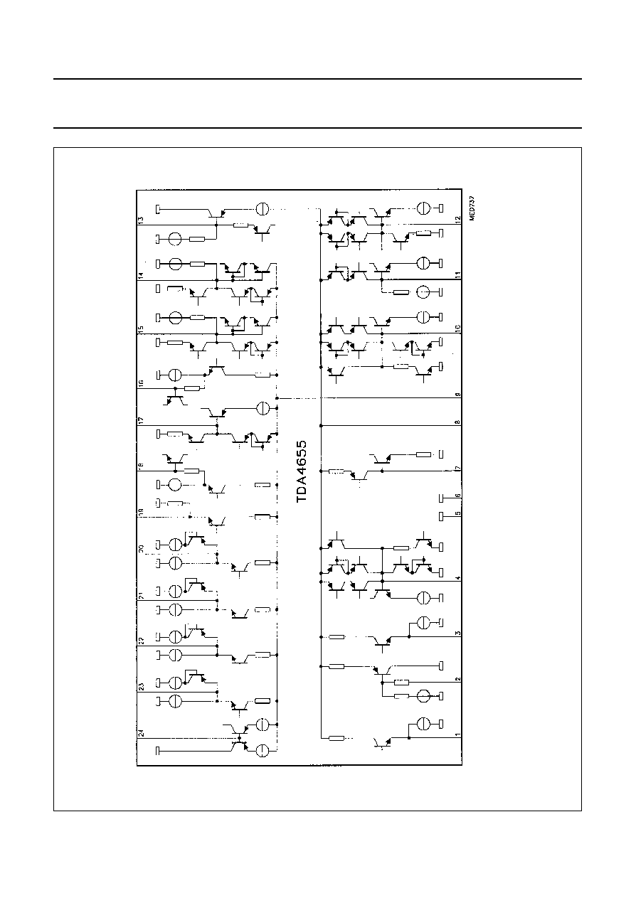
Fig.3 Internal circuits.
June 1993
13
Philips Semiconductors
Preliminary specification
Generic multi-standard decoder
TDA4655
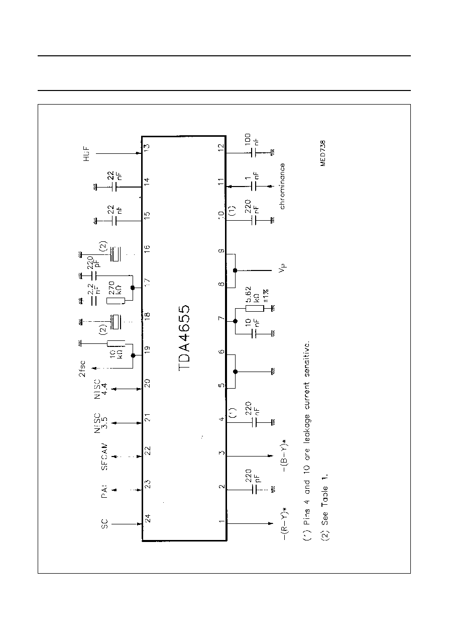
Fig.4 Application circuit.

June 1993
14
Philips Semiconductors
Preliminary specification
Generic multi-standard decoder
TDA4655
PACKAGE OUTLINES
UNIT
b
1
c
E
e
M
H
L
REFERENCES
OUTLINE
VERSION
EUROPEAN
PROJECTION
ISSUE DATE
IEC
JEDEC
EIAJ
mm
DIMENSIONS (mm are the original dimensions)
SOT234-1
92-11-17
95-02-04
b
max.
w
M
E
e
1
1.3
0.8
0.53
0.40
0.32
0.23
22.3
21.4
9.1
8.7
3.2
2.8
0.18
1.778
10.16
10.7
10.2
12.2
10.5
1.6
4.7
0.51
3.8
M
H
c
(e )
1
M
E
A
L
seating plane
A
1
w
M
b
1
e
D
A
2
Z
24
1
13
12
b
E
pin 1 index
0
5
10 mm
scale
Note
1. Plastic or metal protrusions of 0.25 mm maximum per side are not included.
(1)
(1)
D
(1)
Z
A
max.
1
2
A
min.
A
max.
SDIP24: plastic shrink dual in-line package; 24 leads (400 mil)
SOT234-1

June 1993
15
Philips Semiconductors
Preliminary specification
Generic multi-standard decoder
TDA4655
UNIT
A
max.
A
1
A
2
A
3
b
p
c
D
(1)
E
(1)
(1)
e
H
E
L
L
p
Q
Z
y
w
v
REFERENCES
OUTLINE
VERSION
EUROPEAN
PROJECTION
ISSUE DATE
IEC
JEDEC
EIAJ
mm
inches
2.65
0.30
0.10
2.45
2.25
0.49
0.36
0.32
0.23
15.6
15.2
7.6
7.4
1.27
10.65
10.00
1.1
1.0
0.9
0.4
8
0
o
o
0.25
0.1
DIMENSIONS (inch dimensions are derived from the original mm dimensions)
Note
1. Plastic or metal protrusions of 0.15 mm maximum per side are not included.
1.1
0.4
SOT137-1
X
12
24
w
M
A
A
1
A
2
b
p
D
H
E
L
p
Q
detail X
E
Z
c
L
v
M
A
13
(A )
3
A
y
0.25
075E05
MS-013AD
pin 1 index
0.10
0.012
0.004
0.096
0.089
0.019
0.014
0.013
0.009
0.61
0.60
0.30
0.29
0.050
1.4
0.055
0.42
0.39
0.043
0.039
0.035
0.016
0.01
0.25
0.01
0.004
0.043
0.016
0.01
92-11-17
95-01-24
e
1
0
5
10 mm
scale
SO24: plastic small outline package; 24 leads; body width 7.5 mm
SOT137-1

June 1993
16
Philips Semiconductors
Preliminary specification
Generic multi-standard decoder
TDA4655
SOLDERING
Introduction
There is no soldering method that is ideal for all IC
packages. Wave soldering is often preferred when
through-hole and surface mounted components are mixed
on one printed-circuit board. However, wave soldering is
not always suitable for surface mounted ICs, or for
printed-circuits with high population densities. In these
situations reflow soldering is often used.
This text gives a very brief insight to a complex technology.
A more in-depth account of soldering ICs can be found in
our
"IC Package Databook" (order code 9398 652 90011).
SDIP
S
OLDERING BY DIPPING OR BY WAVE
The maximum permissible temperature of the solder is
260
∞
C; solder at this temperature must not be in contact
with the joint for more than 5 seconds. The total contact
time of successive solder waves must not exceed
5 seconds.
The device may be mounted up to the seating plane, but
the temperature of the plastic body must not exceed the
specified maximum storage temperature (T
stg max
). If the
printed-circuit board has been pre-heated, forced cooling
may be necessary immediately after soldering to keep the
temperature within the permissible limit.
R
EPAIRING SOLDERED JOINTS
Apply a low voltage soldering iron (less than 24 V) to the
lead(s) of the package, below the seating plane or not
more than 2 mm above it. If the temperature of the
soldering iron bit is less than 300
∞
C it may remain in
contact for up to 10 seconds. If the bit temperature is
between 300 and 400
∞
C, contact may be up to 5 seconds.
SO
R
EFLOW SOLDERING
Reflow soldering techniques are suitable for all SO
packages.
Reflow soldering requires solder paste (a suspension of
fine solder particles, flux and binding agent) to be applied
to the printed-circuit board by screen printing, stencilling or
pressure-syringe dispensing before package placement.
Several techniques exist for reflowing; for example,
thermal conduction by heated belt. Dwell times vary
between 50 and 300 seconds depending on heating
method. Typical reflow temperatures range from
215 to 250
∞
C.
Preheating is necessary to dry the paste and evaporate
the binding agent. Preheating duration: 45 minutes at
45
∞
C.
W
AVE SOLDERING
Wave soldering techniques can be used for all SO
packages if the following conditions are observed:
∑
A double-wave (a turbulent wave with high upward
pressure followed by a smooth laminar wave) soldering
technique should be used.
∑
The longitudinal axis of the package footprint must be
parallel to the solder flow.
∑
The package footprint must incorporate solder thieves at
the downstream end.
During placement and before soldering, the package must
be fixed with a droplet of adhesive. The adhesive can be
applied by screen printing, pin transfer or syringe
dispensing. The package can be soldered after the
adhesive is cured.
Maximum permissible solder temperature is 260
∞
C, and
maximum duration of package immersion in solder is
10 seconds, if cooled to less than 150
∞
C within
6 seconds. Typical dwell time is 4 seconds at 250
∞
C.
A mildly-activated flux will eliminate the need for removal
of corrosive residues in most applications.
R
EPAIRING SOLDERED JOINTS
Fix the component by first soldering two diagonally-
opposite end leads. Use only a low voltage soldering iron
(less than 24 V) applied to the flat part of the lead. Contact
time must be limited to 10 seconds at up to 300
∞
C. When
using a dedicated tool, all other leads can be soldered in
one operation within 2 to 5 seconds between
270 and 320
∞
C.

June 1993
17
Philips Semiconductors
Preliminary specification
Generic multi-standard decoder
TDA4655
DEFINITIONS
LIFE SUPPORT APPLICATIONS
These products are not designed for use in life support appliances, devices, or systems where malfunction of these
products can reasonably be expected to result in personal injury. Philips customers using or selling these products for
use in such applications do so at their own risk and agree to fully indemnify Philips for any damages resulting from such
improper use or sale.
Data sheet status
Objective specification
This data sheet contains target or goal specifications for product development.
Preliminary specification
This data sheet contains preliminary data; supplementary data may be published later.
Product specification
This data sheet contains final product specifications.
Limiting values
Limiting values given are in accordance with the Absolute Maximum Rating System (IEC 134). Stress above one or
more of the limiting values may cause permanent damage to the device. These are stress ratings only and operation
of the device at these or at any other conditions above those given in the Characteristics sections of the specification
is not implied. Exposure to limiting values for extended periods may affect device reliability.
Application information
Where application information is given, it is advisory and does not form part of the specification.