 | –≠–ª–µ–∫—Ç—Ä–æ–Ω–Ω—ã–π –∫–æ–º–ø–æ–Ω–µ–Ω—Ç: TDA4691 | –°–∫–∞—á–∞—Ç—å:  PDF PDF  ZIP ZIP |
Document Outline
- FEATURES
- GENERAL DESCRIPTION
- QUICK REFERENCE DATA
- ORDERING INFORMATION
- PINNING
- FUNCTIONAL DESCRIPTION
- Sync separator
- Sync-output buffer
- Sync processing
- Phase detector (PHI1)
- Time-constant switching
- VCO 13.5 MHz
- VCO-buffer
- ECL-prescaler
- H-divider
- H-logic
- V-divider
- V-logic
- H-pulse former
- H-pulse buffer
- V-pulse buffer
- Gap reference
- 50/60 Hz output
- SSC generator
- Signal identification with Digital PLL (DPLL)
- Noise detector
- LIMITING VALUES
- THERMAL RESISTANCE
- CHARACTERISTICS
- PACKAGE OUTLINES
- SOLDERING
- DEFINITIONS
- LIFE SUPPORT APPLICATIONS

DATA SHEET
Preliminary specification
File under Integrated Circuits, IC02
September 1993
INTEGRATED CIRCUITS
TDA4691
Sync Processor with Clock (SPC)

September 1993
2
Philips Semiconductors
Preliminary specification
Sync Processor with Clock (SPC)
TDA4691
FEATURES
∑
Sync processor for horizontal (H)
and vertical (V) sync pulses
generated by internal 13.5 MHz
oscillator
∑
Stable `On Screen Display (OSD)',
if no input signal is present with free
running internal oscillator;
automatic turn over to locked
oscillator, if input signal is available
∑
External clock oscillator can be
used
∑
Standard 50/60 Hz signals are
identified automatically
∑
Additional outputs for 13.5 MHz,
composite sync, 50//60 Hz
identification, signal identification
(mute), super-sandcastle 12 V
∑
TTL compatible outputs (H, V,
composite sync and 13.5 MHz)
∑
3 different time constants for the
PHI1 PLL: fast, normal and slow
(T
1
, T
2
and T
3
). Fast and normal
time constant are set independent
from each other
∑
Start of H-pulse definable by
application
∑
Digital interference reduction for H
and V signals
∑
Digital noise detector
∑
Time correction of non-standard
H-pulses and equalizing pulses for
optimum PLL control.
GENERAL DESCRIPTION
The TDA4691 is a bipolar integrated
circuit for sync processing in 50/100
and 60/120 Hz TV sets, preferably in
conjunction with the programmable
deflection controller TDA9150. A line
locked 13.5 MHz clock with several
dividers and logic circuitry is available
generating the horizontal and vertical
sync outputs. The device can be
assembled in a DIL20 or SO20
package.
QUICK REFERENCE DATA
ORDERING INFORMATION
Note
1. SOT146-1; 1996 December 9.
2. SOT4163-1; 1996 December 9.
SYMBOL
PARAMETER
CONDITIONS
MIN.
TYP.
MAX.
UNIT
Supply
V
P2
supply voltage
4.5
5.0
5.5
V
I
P2
supply current
-
-
30
mA
V
P1
supply voltage
7.2
8.0
8.8
V
I
P1
supply current
-
-
30
mA
P
tot
total power
dissipation
-
260
430
mW
Inputs
V
20
input voltage
R
G
= 1 k
-
1
2
V
Outputs
V
4
signal
identification
voltage
no signal;
1 mA
-
-
0.3
V
signal
open
collector
-
V
P1
V
V
7
50/60 Hz
voltage
50 Hz; 1 mA
-
-
0.3
V
60 Hz
open
collector
-
V
P1
V
V
10
vertical output
voltage
HIGH;
-
1 to 0 mA
2.7
-
V
P2
V
LOW; 2 mA
-
-
0.8
V
V
11
horizontal
output voltage
HIGH;
-
1 to 0 mA
2.7
-
V
P2
V
LOW; 2 mA
-
-
0.8
V
V
13
clock output
voltage
HIGH;
-
1 to 0 mA
2.7
-
V
P2
V
LOW; 2 mA
-
-
0.8
V
EXTENDED
TYPE NUMBER
PACKAGE
PINS
PIN
POSITION
MATERIAL
CODE
TDA4691
20
DIL
plastic
SOT146
(1)
TDA4691T
20
SO
plastic
SOT163
(2)
September
1993
3
Philips Semiconductors
Preliminary specification
Sync Processor with Clock (SPC)
TDA4691
This text is here in white to force landscape pages to be rotated correctly when browsing through the pdf in the Acrobat reader.This text is here in
_
white to force landscape pages to be rotated correctly when browsing through the pdf in the Acrobat reader.This text is here inThis text is here in
white to force landscape pages to be rotated correctly when browsing through the pdf in the Acrobat reader. white to force landscape pages to be ...
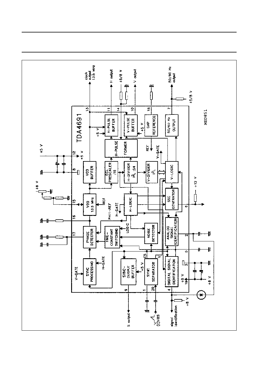
Fig.1 Block diagram.
September 1993
4
Philips Semiconductors
Preliminary specification
Sync Processor with Clock (SPC)
TDA4691
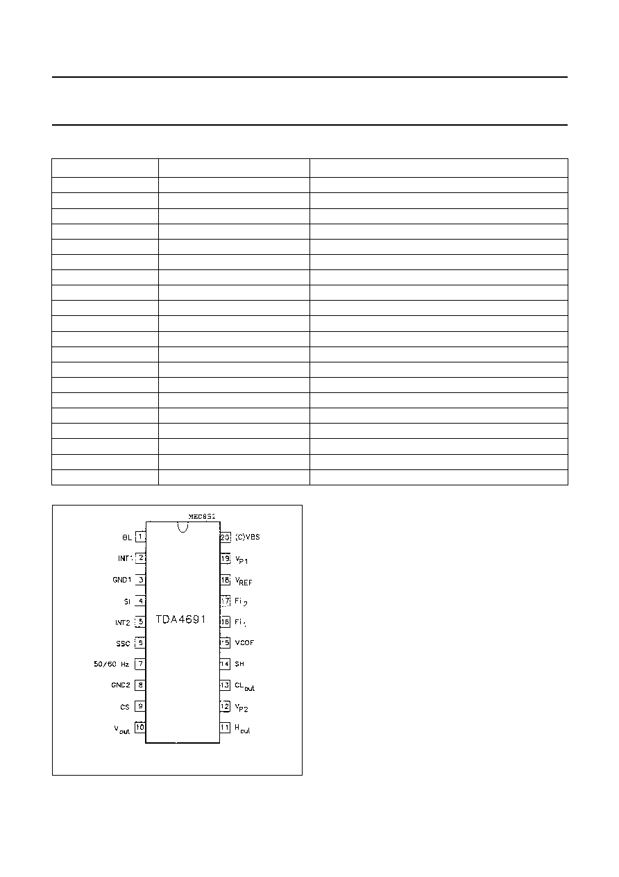
PINNING
SYMBOL
PIN
DESCRIPTION
BL
1
black level storage of sync separator
INT1
2
integration for time constant switching
GND1
3
ground for 8 V supply
SI
4
signal identification output
INT2
5
integration for signal identification
SSC
6
sandcastle output
50/60 Hz
7
50/60 Hz output
GND2
8
ground for 5 V supply
CS
9
sync output
V
out
10
V-output buffer
H
out
11
H-output buffer
V
P2
12
supply 5 V
CL
out
13
clock-output buffer
SH
14
start of H-pulse
VCOF
15
current defining VCO frequency
Fi
1
16
phase detector filtering
Fi
2
17
phase detector filtering
V
REF
18
reference voltage
V
P1
19
supply 8 V
(C)VBS
20
input sync separator
Fig.2 Pin configuration.

September 1993
5
Philips Semiconductors
Preliminary specification
Sync Processor with Clock (SPC)
TDA4691
FUNCTIONAL DESCRIPTION
(See block diagram Fig.1 and timing
Figs 12 to 16)
Sync separator
Top-sync and blacklevel are stored
and H and V sync pulses are sliced in
the middle of both levels (50%).
Sync-output buffer
This circuit turns the current pulse
from the sync separator into a TTL
signal.
Sync processing
This circuit assures that phase
comparison can operate correctly
during V-pulses. Phase jumps
initiated by alternating headpulses of
VCR recorders are quickly recovered.
The sync processing contains the
functions H/2 suppression, sync
extension and sync interruption.
These three functions are only active
if successive pulses have a minimum
distance of 1.6
µ
s.
The H/2 suppression operates with a
gate
-
15
µ
s up to
+
14
µ
s around the
PHI1-reference and is necessary for
suppression of the equalizing pulses.
For sync interruption this gate is
closed earlier if the detected sync is
longer than 4.8
µ
s.
Only during V-pulses will the duration
of the applied pulses be tested. If they
are longer than 1.6
µ
s they will be
recognized as sync pulses and
enlarged up to 4.6
µ
s.
Phase detector (PHI1)
The phase detector has separate
filters for the fast time constant T
1
(pin
17) and normal time constant T
2
(pins
17 and 16). The slow time constant T
3
uses the normal time constant T
2
with
reduced control current. For reduction
of H-pulse modulation the filter at pin
16 is switched off during sync time if
normal time constant T
2
is on. Thus
no frequency shifting of the oscillator
is possible during sync.
Time-constant switching
This block contains a switch and an
impedance converter (buffer). The
switch connects the filters at pin 16
and 17 in parallel (normal time
constant T
2
or slow time constant T
3
).
The buffer transfers the control
voltage at pin 17 to pin 16 (fast time
constant T
1
). Which of the 2 functions
is active is determined by the blocks
noise detector, V-logic or signal
identification.
VCO 13.5 MHz
The adjustment of the nominal
frequency (13.5 MHz) is achieved at
pin 15. The VCO control voltage is
applied (from the phase detector) at
pin 16.
The control range can be adjusted by
the current at pin 18.
Pin 15 can be used to feed in an
external frequency. Under these
circumstances the internal VCO is
switched off by application.
The control voltage at pin 16 can be
used to control the external VCO.
VCO-buffer
The VCO-buffer delivers a TTL
compatible signal of 13.5 MHz to pin
13.
ECL-prescaler
This block consists of a :16
asynchronous prescaler.
H-divider
This is a divider by 54. It is split into a
prescaler :2 and a divider by 27. Out
of this block several signals are taken
for generation of H-frequently pulses
in the H-logic block. These signals
must have good timing. This is
achieved by special synchronization.
H-logic
This block creates all pulses
necessary for the SSC generator, the
signal identification, the phase
detector, the sync preparation and the
V-divider.
V-divider
The V-divider consists of an
asynchronous 10-bit divider and a
decoder logic. The divider is clocked
with twice the line frequency. The
decoder circuit delivers the pulses
necessary for the V-logic.
V-logic
In the V-logic the V-syncs from the
sync separator are evaluated and
noise reduced. Also certain operation
states are switched ON and OFF.
Additionally the reset pulse for the
V-divider and the 50/60 Hz
information is generated.
H-pulse former
The H-pulse starting point can be
shifted in this stage, also the gate
pulse of
2.4
µ
s is generated for use
in the digital noise identification block.
H-pulse buffer
In this circuit the line signal will be
pre-synchronized by output signal of
the :16 divider and synchronized by
the 13.5 MHz clock. The buffer
delivers TTL output signals.
V-pulse buffer
The signal out of the V-divider is
synchronized with 13.5 MHz clock
and converted to a TTL output level.
Gap reference
This circuit operates with the
gap-principle and is stable with regard
to temperature and supply voltage
changes.

September 1993
6
Philips Semiconductors
Preliminary specification
Sync Processor with Clock (SPC)
TDA4691
50/60 Hz output
This is an open-collector output,
which is LOW if more than 287
lines/field are detected.
SSC generator
The SSC generator generates a 3
stage super-sandcastle pulse on an
open-collector output, which is able to
operate up to 12 volts. The blanking
thresholds 2.5 V and 4.5 V are
derived from the gap reference (point
16).
Signal identification with Digital
PLL (DPLL)
The analog signal identification with
output signal at pin 4 is completed
with a DPLL. This PLL is able to lock
on the separated sync although the
13.5 MHz VCO is not locked on the
input signal. The ratio of the lock
condition to the unlock condition
influences the voltage at pin 5. The
detector circuit of the analog signal
identification block evaluates the
voltages at pins 2 and 5. If the voltage
at pin 5 reaches 4 V (most of the time
the PLL is locked) pin 4 will be HIGH.
The voltages at pins 2 and 5 together
with the state of the V-logic set the
operation state of the TDA4691. The
TDA4691 is able to accommodate to
different input conditions
automatically.
Some operation conditions can be
set externally by influencing the
voltages at pins 2 and 5:
1. Time constant T
1
(fast) on:
voltage at pin 2 is limited to
5 V (0 to 5 V).
2. Time constant T
3
(slow) on:
voltage at pin 5 is limited to
6.2 V (0 to 6.2 V).
3. Time constant T
3
(slow)
inoperative:
voltage at pin 2 is limited
between 4 V and 6.5 V.
4. Time constant T
3
(slow)
inoperative with input signal:
voltage at pin 2 is limited to
6.5 V (0 to 6.5 V).
5. VCO frequency fixed to f
0
:
pin 2 is set to ground
(V
2
<
1 V).
Noise detector
This block switches the time
constant to `slow' if on standard
signal a certain noise level is
reached. This noise level is
measured in a small window
inside the sync pulse.
September 1993
7
Philips Semiconductors
Preliminary specification
Sync Processor with Clock (SPC)
TDA4691
LIMITING VALUES
In accordance with the Absolute Maximum Rating System (IEC 134).
Note to the limiting values
1. Equivalent to discharging a 200 pF capacitor through a 0
series resistor.
THERMAL RESISTANCE
SYMBOL
PARAMETER
MIN.
MAX.
UNIT
V
P1
supply voltage
0
9.0
V
I
P1
supply current
-
40
mA
V
P2
supply voltage
0
5.7
V
I
P2
supply current
-
50
mA
P
tot
total power dissipation
-
650
mW
T
stg
storage temperature
-
25
+
150
∞
C
T
amb
operating ambient temperature
0
+
70
∞
C
V
ESD
ESD-protection on all pins; note 1
300
-
V
I
I/O
currents on all pins except supply pins 3, 8, 12 and 19
-
10
+
10
mA
V
I
voltage applied to pins 1, 2, 4, 5, 7, 14 and 20
0
V
P1
V
V
I
voltage applied to pins 9, 10, 11 and 13
0
V
P2
V
V
6
voltage applied to pin 6
0
13.2
V
V
15
voltage applied to pin 15
0
5
V
V
16
voltage applied to pin 16
0
5
V
V
17
voltage applied to pin 17
0
5
V
V
18
voltage applied to pin 18
0
5
V
SYMBOL
PARAMETER
THERMAL RESISTANCE
R
th j-a
from junction to ambient in free air
SOT146 (without heat spreader)
65 K/W
SOT163
85 K/W

September 1993
8
Philips Semiconductors
Preliminary specification
Sync Processor with Clock (SPC)
TDA4691
CHARACTERISTICS
V
P1
= 8 V; V
P2
= 5 V; measured at T
amb
=
+
25
∞
C; unless otherwise specified; application see Figs 10 and 11; video
input signal referenced to CCIR standard.
SYMBOL
PARAMETER
CONDITIONS
MIN.
TYP.
MAX.
UNIT
Supply (pins 19 and 12; all voltages are measured with regard to ground (pins 3 and 8))
V
19
supply voltage
7.2
8.0
8.8
V
I
P1
supply current
-
20
30
mA
V
12
supply voltage
same rise time as V
19
4.5
5.0
5.5
V
I
P2
supply current
-
15
30
mA
P
tot
total power dissipation
-
260
430
mW
Sync separator (pin 20)
V
20(p-p)
input voltage (peak-to-peak value)
AC coupled
-
1
2
V
V
20(p-p)
sync amplitude (peak-to-peak value)
0.1
-
0.6
V
R
G
source resistor of generator
-
-
1
k
I
20
current during sync
-
-
30
-
µ
A
I
20
current during remaining time
-
1
-
µ
A
Black level (pin 1)
SLH
slicing level H
-
50
-
%
SLV
slicing level V
-
50
-
%
Sync output (pin 9)
V
9
no sync
I
9
=
+
1 mA
-
0.3
-
V
V
9
positive sync
I
9
=
-
1 mA
2.7
-
V
12
V
C
L
load capacitance
-
-
40
pF
t
1
time delay between pin 20 and pin 9
see Fig.3
100
200
500
ns
t
2
time delay between pin 20 and pin 9
see Fig.3
100
300
500
ns
Phase detector (pins 16 and 17)
f
0
nominal sync frequency
-
15.625
-
kHz
f
0
'
f
osc
: 864 = phiref
-
15.625
-
kHz
I
17
current at sync time
(fast and normal time constant)
-
±
240
-
µ
A
I
17
current at sync time (slow time constant)
-
±
80
-
µ
A
I
16
current at sync time
time constant T
1
-
±
2
-
mA
V
17
filter 2 voltage
1.5
3
4.5
V
V
16
filter 1 voltage
1.5
3
4.5
V
f
0
/
V
16
VCO sensitivity
see VCO
-
360
-
kHz/V
13.5 MHz VCO (pin 15)
R
15
f
0
defining resistor
see Fig.4(a)
-
3.75
-
k
V
15
pin voltage (V
19
dependent)
see Fig.4(a)
2.9
3
3.1
V
I
15
current for 13.5 MHz
-
720
-
800
-
880
µ
A
g
VCO
transconductance at f
0
15.2
-
18.6
kHz/
µ
A

September 1993
9
Philips Semiconductors
Preliminary specification
Sync Processor with Clock (SPC)
TDA4691
f
0
/
V
16
VCO sensitivity
4% control range;
depending on current
at pin 18
-
360
-
kHz/V
Input of external oscillator (pin 15)
V
15
pin voltage AC
see Fig.4(b)
1
-
3
V
V
15
pin voltage DC
dependent on V
19
-
5
-
V
R
int
internal resistance
see Fig.4(b)
-
7
-
k
C
int
internal capacitance
see Fig.4(b)
-
4
-
pF
13.5 MHz buffer (pin 13)
V
13
clock HIGH level output voltage
I
13
=
-
1 mA;
V
12
= 4.5 V
2.7
-
V
12
V
V
13
clock HIGH level output voltage
I
13
= 0 mA
2.7
-
V
12
V
V
13
clock LOW level output voltage
I
13
= 2 mA;
V
12
= 5.5 V
0
-
0.8
V
t
r
rise time
see Fig.5
-
20
-
ns
t
f
fall time
see Fig.5
-
20
-
ns
D
13
mark-to-space ratio
V
13
= 1.5 V
45/55
-
55/45
%
C
L
load capacitance
-
-
40
pF
T
13
jitter on clock output
(peak-to-peak value)
normal time constant
T
2;
measured between
lines 25 and 305
-
-
2
ns
H-output buffer (pin 11)
V
11
H HIGH level output voltage
I
11
=
-
1 mA;
V
12
= 4.5 V
2.7
-
V
12
V
V
11
H HIGH level output voltage
I
11
= 0 mA
2.7
-
V
12
V
V
11
H LOW level output voltage
I
11
= 2 mA;
V
12
= 5.5 V
0
-
0.8
V
t
r
rise time
see Fig.6
-
25
-
ns
t
f
fall time
see Fig.6
-
25
-
ns
t
3
time relation pin 13 to 11
see Fig.6
-
25
55
ns
t
4
time relation pin 13 to 11
see Fig.6
3
-
-
ns
t
5
H-pulse width
see Fig.6
3.0
3.6
4.2
µ
s
C
L
load capacitance
see Fig.6
-
-
40
pF
Start of H-pulse (pin 14)
I
14
current pin 14
-
-
±
100
µ
A
t
61
time delay pulse between pin 20 and 11
see Fig.6
-
1.1
-
1.3
-
1.5
µ
s
t
62
time delay pulse between pin 20 and 11
see Fig.6
-
0.6
-
0.8
-
1.0
µ
s
t
63
time delay pulse between pin 20 and 11
see Fig.6
3.8
4.0
4.2
µ
s
t
64
time delay pulse between pin 20 and 11
see Fig.6
5.0
5.2
5.4
µ
s
V
14
(t
61
)
voltage pin 14 (proportional to V
19
)
0
-
1
V
SYMBOL
PARAMETER
CONDITIONS
MIN.
TYP.
MAX.
UNIT

September 1993
10
Philips Semiconductors
Preliminary specification
Sync Processor with Clock (SPC)
TDA4691
V
14
(t
62
)
voltage pin 14 (proportional to V
19
)
2
2.4
2.8
V
V
14
(t
63
)
voltage pin 14 (proportional to V
19
)
3.5
4
4.5
V
V
14
(t
64
)
voltage pin 14 (proportional to V
19
)
5
5.5
6
V
V-output buffer (pin 10)
V
10
V HIGH level output voltage
I
10
=
-
1 mA;
V
12
= 4.5 V
2.7
-
V
12
V
V
10
V HIGH level output voltage
I
10
= 0 mA
2.7
-
V
12
V
V
10
V LOW level output voltage
I
10
= 2 mA;
V
12
= 5.5 V
0
-
0.8
V
t
r
rise time
see Fig.6
-
25
-
ns
t
f
fall time
see Fig.6
-
25
-
ns
t
3
time relation pin 13 to 10
see Fig.6
-
25
55
ns
t
4
time relation pin 13 to 10
see Fig.6
3
-
-
ns
t
5
V-pulse width
see Fig.7
280
320
350
µ
s
t
6
time delay between pin 20 and pin 10
see Fig.7
12
16
20
µ
s
C
L
load capacitance
see Fig.7
-
-
40
pF
Reference (pin 18)
V
REF
reference voltage
1.1
1.2
1.3
V
R
18
control current defining resistor
8
-
30
k
f
control range VCO
-
±
4
-
%
I
18/1
current pin 18 (
±
4%)
-
105
-
µ
A
f
a
adjustable control range
±
3
-
±
5
%
I
18/3
current pin 18 (
±
3%)
-
80
-
µ
A
I
18/3
current pin 18 (
±
5%)
-
120
-
µ
A
50/60 Hz output (pin 7; open collector; see Fig.8)
V
7
output voltage pin 7; 50 Hz
287.5 lines/field = LOW
I
7
= 1 mA
0
-
0.3
V
I
7
= 2 mA
0
0.3
0.8
V
V
7
output voltage pin 7; 60 Hz
287 lines/field = HIGH
2.7
-
V
19
V
I
7
output leakage current
-
-
50
µ
A
Sandcastle output (pin 6)
V
6
burstkey pulse
see Fig.9
9.5
10
12
V
V
6
H-blanking pulse
independent from V
supply
4.3
4.5
4.7
V
V
6
V-blanking pulse
independent from V
supply
2.3
2.5
2.7
V
V
6
voltage pin 6 LOW
0
0.2
0.8
V
t
w
pulse width burstkey; 50 Hz
at 6.5 V; see Fig.9
4.0
4.3
4.7
µ
s
t
w
pulse width burstkey; 60 Hz
at 6.5 V; see Fig.9
3.3
3.8
4.1
µ
s
t
2
time relation between pin 20 and
burstkey
see Fig.9
2.2
2.5
2.8
µ
s
SYMBOL
PARAMETER
CONDITIONS
MIN.
TYP.
MAX.
UNIT
September 1993
11
Philips Semiconductors
Preliminary specification
Sync Processor with Clock (SPC)
TDA4691
t
3
time relation between pin 20 and
blanking
see Fig.9
3.5
4.0
4.5
µ
s
t
4
H-blanking time
see Fig.9
-
11.8
-
µ
s
t
5
start time H-pulse pin 20 to stop time
burstkey pin 6; 50 Hz
H-sync = 4.7
µ
s;
see Fig.9
8.0
9.0
9.7
µ
s
t
5
start time H-pulse pin 20 to stop time
burstkey pin 6; 60 Hz
see Fig.9
7.5
8.6
9.2
µ
s
t
6
V-blanking pulse; 50 Hz
-
-
2.5 to
+
22.5
-
lines
t
6
V-blanking pulse; 60 Hz
-
-
3.0 to
+
17
-
lines
Integration (pin 5)
V
5
no TV signal
see Fig.16
0
-
2
V
TV signal
see Fig.16
4
-
-
V
V
5
slow time constant on
5
-
6.2
V
Signal identification (pin 4; open collector via R
4
to V
19
or V
12
)
V
4
voltage pin 4, if no signal is identified
I
4
= 1 mA
0
-
0.3
V
I
4
= 5 mA
0
0.2
0.8
V
V
4
voltage pin 4, if signal is identified
-
-
V
19
V
I
4
leakage current
-
-
50
µ
A
Integration (pin 2; see Fig.15)
V
2
no signal at pin 20
-
1.5
-
V
V
2
noise at input pin 20
-
3
-
V
V
2
switching T
3
to T
1
(delay 7 fields)
-
2.5
-
V
V
2
switching T
3
to T
1
(noise and signal at input pin 20)
-
2.5
-
V
V
2
release V-divider
-
4
-
V
hysteresis
-
-
0.2
-
V
V
2
release time constant normal (T
2
)
signal identification at pin 4
-
5
-
V
hysteresis
-
-
0.2
-
V
V
2
release noise detector
-
6.5
-
V
SYMBOL
PARAMETER
CONDITIONS
MIN.
TYP.
MAX.
UNIT

September 1993
12
Philips Semiconductors
Preliminary specification
Sync Processor with Clock (SPC)
TDA4691
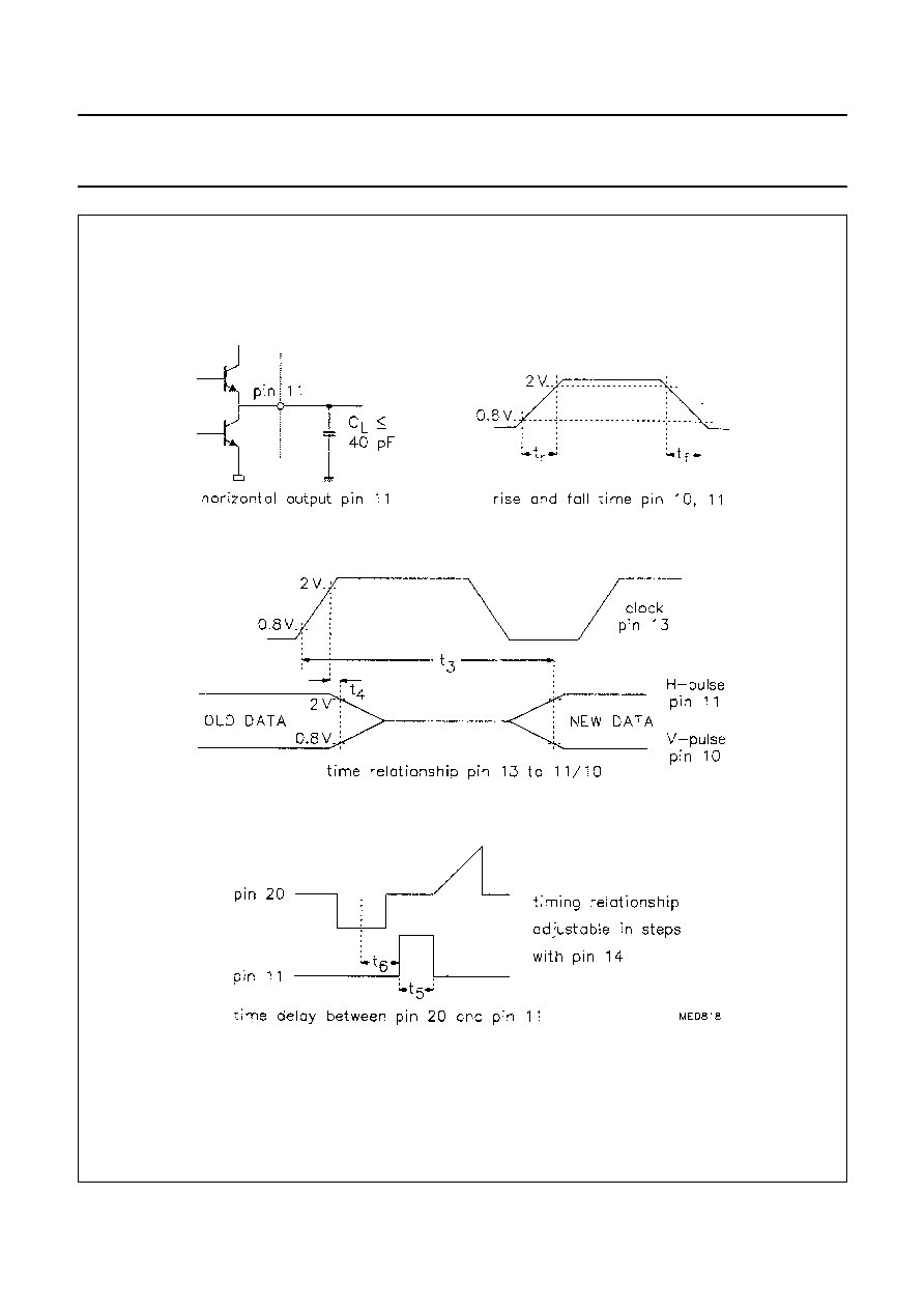
Fig.3 Sync output.
Fig.4 Pin 15 circuit for (a) internal VCO; (b) external VCO.
Fig.5 Clock output.
September 1993
13
Philips Semiconductors
Preliminary specification
Sync Processor with Clock (SPC)
TDA4691
Fig.6 Time relationship of pin 10/11 to pin 13/20.
September 1993
14
Philips Semiconductors
Preliminary specification
Sync Processor with Clock (SPC)
TDA4691
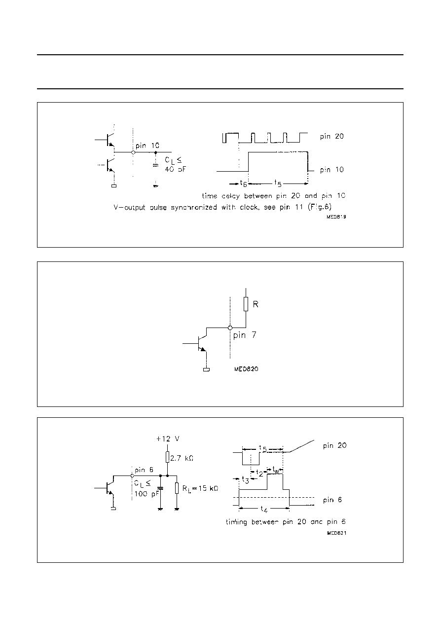
Fig.7 Time relationship pin 10 to pin 20.
Fig.8 50/60 Hz output.
Fig.9 Sandcastle output.

September
1993
15
Philips Semiconductors
Preliminary specification
Sync Processor with Clock (SPC)
TDA4691
This text is here in white to force landscape pages to be rotated correctly when browsing through the pdf in the Acrobat reader.This text is here in
_
white to force landscape pages to be rotated correctly when browsing through the pdf in the Acrobat reader.This text is here inThis text is here in
white to force landscape pages to be rotated correctly when browsing through the pdf in the Acrobat reader. white to force landscape pages to be ...
Fig.10 Application diagram.
(1) control range VCO 4%; see CHARACTERISTICS.
(2) depending on H output shift; see CHARACTERISTICS.
V
P
(V)
R2 (k
)
5
5.1
8
8.2

September
1993
16
Philips Semiconductors
Preliminary specification
Sync Processor with Clock (SPC)
TDA4691
This text is here in white to force landscape pages to be rotated correctly when browsing through the pdf in the Acrobat reader.This text is here in
_
white to force landscape pages to be rotated correctly when browsing through the pdf in the Acrobat reader.This text is here inThis text is here in
white to force landscape pages to be rotated correctly when browsing through the pdf in the Acrobat reader. white to force landscape pages to be ...
Fig.11 TDA4691 with external VCO and prescaler.
(1) control range VCO 4%; see CHARACTERISTICS.
(2) depending on H output shift; see CHARACTERISTICS.
V
P
(V)
R2 (k
)
5
5.1
8
8.2
September 1993
17
Philips Semiconductors
Preliminary specification
Sync Processor with Clock (SPC)
TDA4691
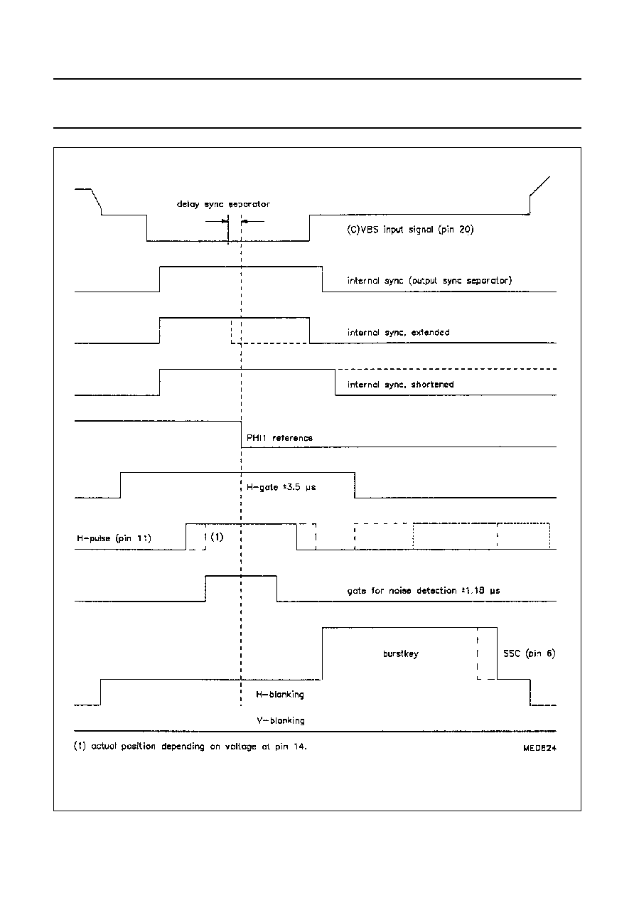
Fig.12 H-timing overview.

September
1993
18
Philips Semiconductors
Preliminary specification
Sync Processor with Clock (SPC)
TDA4691
This text is here in white to force landscape pages to be rotated correctly when browsing through the pdf in the Acrobat reader.This text is here in
_
white to force landscape pages to be rotated correctly when browsing through the pdf in the Acrobat reader.This text is here inThis text is here in
white to force landscape pages to be rotated correctly when browsing through the pdf in the Acrobat reader. white to force landscape pages to be ...
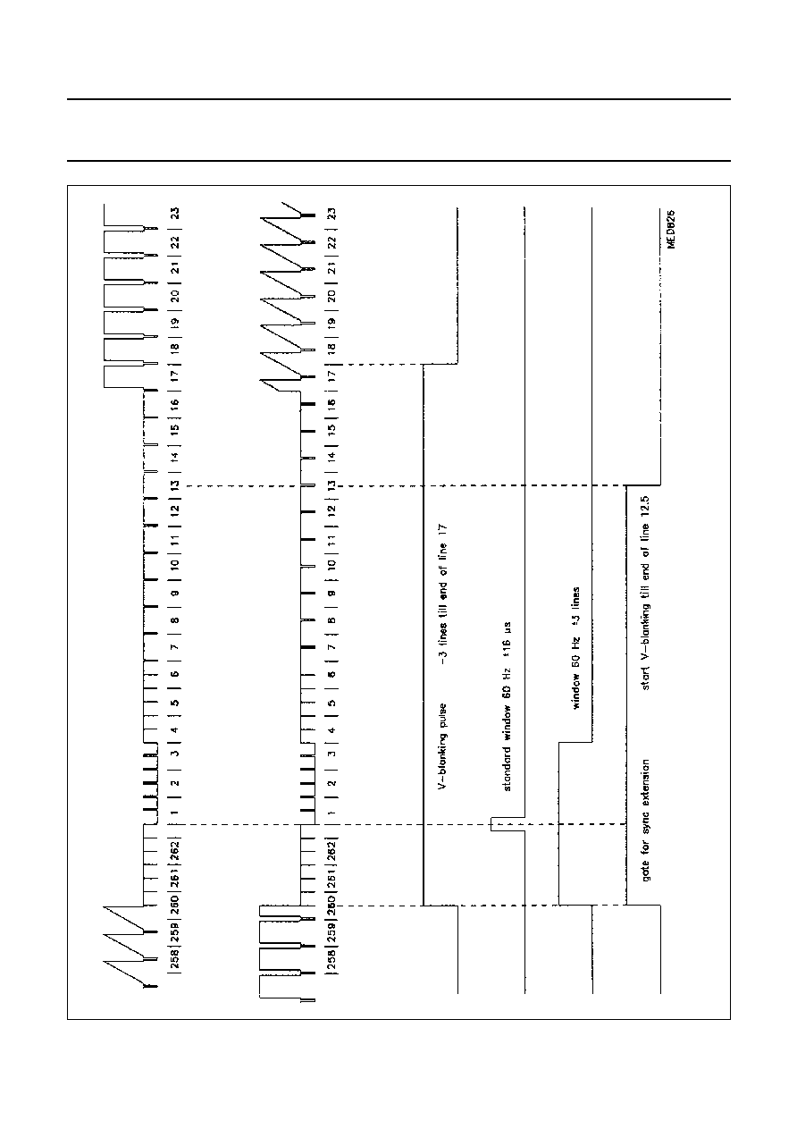
Fig.13 V-timing at 50 Hz operation.
September
1993
19
Philips Semiconductors
Preliminary specification
Sync Processor with Clock (SPC)
TDA4691
This text is here in white to force landscape pages to be rotated correctly when browsing through the pdf in the Acrobat reader.This text is here in
_
white to force landscape pages to be rotated correctly when browsing through the pdf in the Acrobat reader.This text is here inThis text is here in
white to force landscape pages to be rotated correctly when browsing through the pdf in the Acrobat reader. white to force landscape pages to be ...
Fig.14 V-timing at 60 Hz operation.

September 1993
20
Philips Semiconductors
Preliminary specification
Sync Processor with Clock (SPC)
TDA4691
Fig.15 Control of operation states by voltage at pin 2.

September 1993
21
Philips Semiconductors
Preliminary specification
Sync Processor with Clock (SPC)
TDA4691
Fig.16 Control of signal identification (pin 4) and time constants by voltage at pin 5.
September 1993
22
Philips Semiconductors
Preliminary specification
Sync Processor with Clock (SPC)
TDA4691
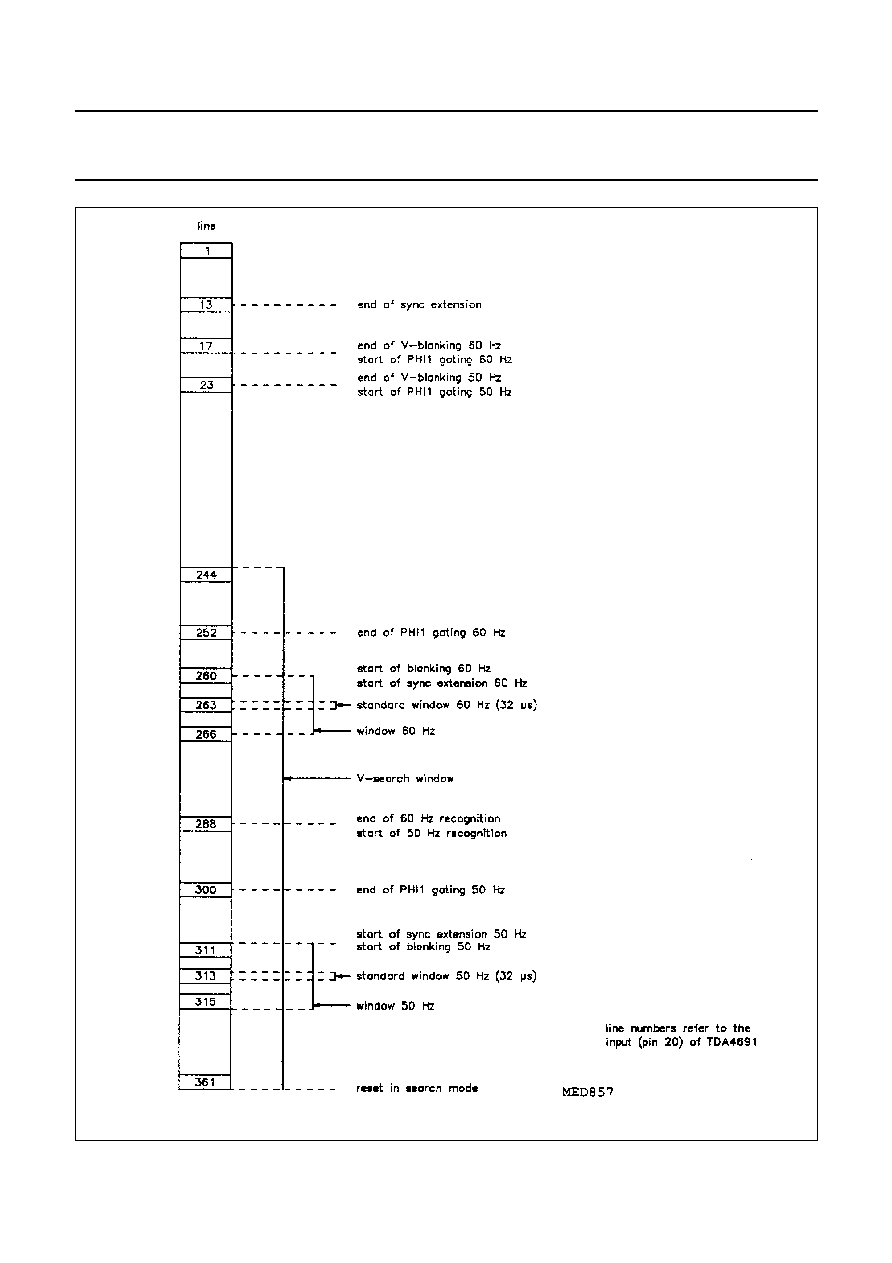
Fig.17 V-timing.

September 1993
23
Philips Semiconductors
Preliminary specification
Sync Processor with Clock (SPC)
TDA4691
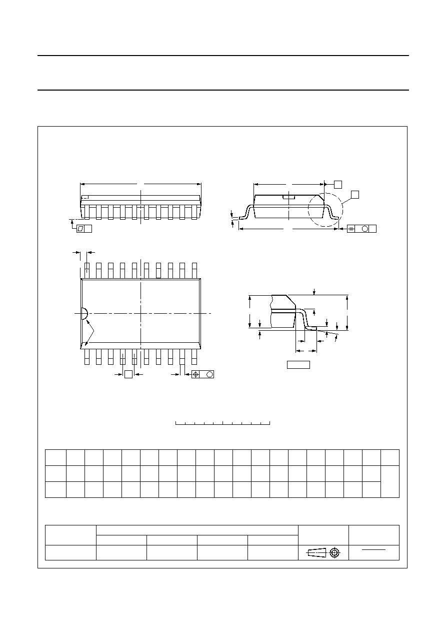
PACKAGE OUTLINES
UNIT
A
max.
1
2
b
1
c
D
E
e
M
H
L
REFERENCES
OUTLINE
VERSION
EUROPEAN
PROJECTION
ISSUE DATE
IEC
JEDEC
EIAJ
mm
inches
DIMENSIONS (inch dimensions are derived from the original mm dimensions)
SOT146-1
92-11-17
95-05-24
A
min.
A
max.
b
Z
max.
w
M
E
e
1
1.73
1.30
0.53
0.38
0.36
0.23
26.92
26.54
6.40
6.22
3.60
3.05
0.254
2.54
7.62
8.25
7.80
10.0
8.3
2.0
4.2
0.51
3.2
0.068
0.051
0.021
0.015
0.014
0.009
1.060
1.045
0.25
0.24
0.14
0.12
0.01
0.10
0.30
0.32
0.31
0.39
0.33
0.078
0.17
0.020
0.13
SC603
M
H
c
(e )
1
M
E
A
L
seating plane
A
1
w
M
b
1
e
D
A
2
Z
20
1
11
10
b
E
pin 1 index
0
5
10 mm
scale
Note
1. Plastic or metal protrusions of 0.25 mm maximum per side are not included.
(1)
(1)
(1)
DIP20: plastic dual in-line package; 20 leads (300 mil)
SOT146-1
September 1993
24
Philips Semiconductors
Preliminary specification
Sync Processor with Clock (SPC)
TDA4691
UNIT
A
max.
A
1
A
2
A
3
b
p
c
D
(1)
E
(1)
(1)
e
H
E
L
L
p
Q
Z
y
w
v
REFERENCES
OUTLINE
VERSION
EUROPEAN
PROJECTION
ISSUE DATE
IEC
JEDEC
EIAJ
mm
inches
2.65
0.30
0.10
2.45
2.25
0.49
0.36
0.32
0.23
13.0
12.6
7.6
7.4
1.27
10.65
10.00
1.1
1.0
0.9
0.4
8
0
o
o
0.25
0.1
DIMENSIONS (inch dimensions are derived from the original mm dimensions)
Note
1. Plastic or metal protrusions of 0.15 mm maximum per side are not included.
1.1
0.4
SOT163-1
10
20
w
M
b
p
detail X
Z
e
11
1
D
y
0.25
075E04
MS-013AC
pin 1 index
0.10
0.012
0.004
0.096
0.089
0.019
0.014
0.013
0.009
0.51
0.49
0.30
0.29
0.050
1.4
0.055
0.419
0.394
0.043
0.039
0.035
0.016
0.01
0.25
0.01
0.004
0.043
0.016
0.01
0
5
10 mm
scale
X
A
A
1
A
2
H
E
L
p
Q
E
c
L
v
M
A
(A )
3
A
SO20: plastic small outline package; 20 leads; body width 7.5 mm
SOT163-1
95-01-24
97-05-22

September 1993
25
Philips Semiconductors
Preliminary specification
Sync Processor with Clock (SPC)
TDA4691
SOLDERING
Introduction
There is no soldering method that is ideal for all IC
packages. Wave soldering is often preferred when
through-hole and surface mounted components are mixed
on one printed-circuit board. However, wave soldering is
not always suitable for surface mounted ICs, or for
printed-circuits with high population densities. In these
situations reflow soldering is often used.
This text gives a very brief insight to a complex technology.
A more in-depth account of soldering ICs can be found in
our
"IC Package Databook" (order code 9398 652 90011).
DIP
S
OLDERING BY DIPPING OR BY WAVE
The maximum permissible temperature of the solder is
260
∞
C; solder at this temperature must not be in contact
with the joint for more than 5 seconds. The total contact
time of successive solder waves must not exceed
5 seconds.
The device may be mounted up to the seating plane, but
the temperature of the plastic body must not exceed the
specified maximum storage temperature (T
stg max
). If the
printed-circuit board has been pre-heated, forced cooling
may be necessary immediately after soldering to keep the
temperature within the permissible limit.
R
EPAIRING SOLDERED JOINTS
Apply a low voltage soldering iron (less than 24 V) to the
lead(s) of the package, below the seating plane or not
more than 2 mm above it. If the temperature of the
soldering iron bit is less than 300
∞
C it may remain in
contact for up to 10 seconds. If the bit temperature is
between 300 and 400
∞
C, contact may be up to 5 seconds.
SO
R
EFLOW SOLDERING
Reflow soldering techniques are suitable for all SO
packages.
Reflow soldering requires solder paste (a suspension of
fine solder particles, flux and binding agent) to be applied
to the printed-circuit board by screen printing, stencilling or
pressure-syringe dispensing before package placement.
Several techniques exist for reflowing; for example,
thermal conduction by heated belt. Dwell times vary
between 50 and 300 seconds depending on heating
method. Typical reflow temperatures range from
215 to 250
∞
C.
Preheating is necessary to dry the paste and evaporate
the binding agent. Preheating duration: 45 minutes at
45
∞
C.
W
AVE SOLDERING
Wave soldering techniques can be used for all SO
packages if the following conditions are observed:
∑
A double-wave (a turbulent wave with high upward
pressure followed by a smooth laminar wave) soldering
technique should be used.
∑
The longitudinal axis of the package footprint must be
parallel to the solder flow.
∑
The package footprint must incorporate solder thieves at
the downstream end.
During placement and before soldering, the package must
be fixed with a droplet of adhesive. The adhesive can be
applied by screen printing, pin transfer or syringe
dispensing. The package can be soldered after the
adhesive is cured.
Maximum permissible solder temperature is 260
∞
C, and
maximum duration of package immersion in solder is
10 seconds, if cooled to less than 150
∞
C within
6 seconds. Typical dwell time is 4 seconds at 250
∞
C.
A mildly-activated flux will eliminate the need for removal
of corrosive residues in most applications.
R
EPAIRING SOLDERED JOINTS
Fix the component by first soldering two diagonally-
opposite end leads. Use only a low voltage soldering iron
(less than 24 V) applied to the flat part of the lead. Contact
time must be limited to 10 seconds at up to 300
∞
C. When
using a dedicated tool, all other leads can be soldered in
one operation within 2 to 5 seconds between
270 and 320
∞
C.
September 1993
26
Philips Semiconductors
Preliminary specification
Sync Processor with Clock (SPC)
TDA4691
DEFINITIONS
LIFE SUPPORT APPLICATIONS
These products are not designed for use in life support appliances, devices, or systems where malfunction of these
products can reasonably be expected to result in personal injury. Philips customers using or selling these products for
use in such applications do so at their own risk and agree to fully indemnify Philips for any damages resulting from such
improper use or sale.
Data sheet status
Objective specification
This data sheet contains target or goal specifications for product development.
Preliminary specification
This data sheet contains preliminary data; supplementary data may be published later.
Product specification
This data sheet contains final product specifications.
Limiting values
Limiting values given are in accordance with the Absolute Maximum Rating System (IEC 134). Stress above one or
more of the limiting values may cause permanent damage to the device. These are stress ratings only and operation
of the device at these or at any other conditions above those given in the Characteristics sections of the specification
is not implied. Exposure to limiting values for extended periods may affect device reliability.
Application information
Where application information is given, it is advisory and does not form part of the specification.