 | –≠–ª–µ–∫—Ç—Ä–æ–Ω–Ω—ã–π –∫–æ–º–ø–æ–Ω–µ–Ω—Ç: TDA4820T | –°–∫–∞—á–∞—Ç—å:  PDF PDF  ZIP ZIP |
Document Outline
- FEATURES
- GENERAL DESCRIPTION
- QUICK REFERENCE DATA
- ORDERING AND PACKAGE INFORMATION
- PINNING
- PIN CONFIGURATION
- FUNCTIONAL DESCRIPTION
- Video amplifier and black level clamping
- 50% peak sync voltage
- Composite sync slicing
- Vertical slicing and double slope integrator
- Vertical sync output Composite sync output
- LIMITING VALUES
- CHARACTERISTICS
- PACKAGE OUTLINE
- SOLDERING
- DEFINITIONS
- LIFE SUPPORT APPLICATIONS

DATA SHEET
Preliminary specification
File under Integrated Circuits, IC02
June 1990
INTEGRATED CIRCUITS
TDA4820T
Sync separation circuit for video
applications

June 1990
2
Philips Semiconductors
Preliminary specification
Sync separation circuit for video applications
TDA4820T
FEATURES
∑
Fully integrated, few external components
∑
Positive video input signal, capacitively coupled
∑
Operates with non-standard video input signals
∑
Black level clamping
∑
Generation of composite sync slicing level at 50% of
peak sync voltage
∑
Vertical sync separator with double slope integrator
∑
Delay time of the vertical output pulse is determined by
an external resistor
∑
Vertical sync generation with a slicing level at 40% of
peak sync voltage
∑
Output stage for composite sync
∑
Output stage for vertical sync
GENERAL DESCRIPTION
The TDA4820T is a monolithic integrated circuit including
a horizontal and a vertical sync separator, offering
composite sync and vertical sync extracted from the video
signal.
QUICK REFERENCE DATA
ORDERING AND PACKAGE INFORMATION
Note
1. SOT96-1; 1997 January 08.
SYMBOL
PARAMETER
CONDITIONS
MIN.
TYP.
MAX.
UNIT
V
P
supply voltage range (pin 1)
10.8
12
13.2
V
I
P
supply current (pin 1)
-
8
12
mA
V
2(p-p)
input voltage amplitude (peak-to-peak value)
0.2
1
3
V
V
sync(p-p)
sync pulse input voltage amplitude (pin 2)
(peak-to-peak value)
50
300
500
mV
V
o
maximum vertical sync output voltage (pin 6)
I
6
=
-
1 mA
10.0
-
-
V
V
o
maximum composite sync output voltage
(pin 7)
I
7
=
-
3 mA
10.0
-
-
V
V
o
minimum output voltage (pins 6 and 7)
I
6,7
= 1 mA
-
-
0.6
V
T
amb
operating ambient temperature range
0
-
+
70
∞
C
EXTENDED
TYPE NUMBER
PACKAGE
PINS
PIN POSITION
MATERIAL
CODE
TDA4820T
8
mini-pack
plastic
SO8; SOT96A
(1)

June 1990
3
Philips Semiconductors
Preliminary specification
Sync separation circuit for video applications
TDA4820T
Fig.1 Block diagram and application circuit.
PINNING
SYMBOL
PIN
DESCRIPTION
V
P
1
supply voltage
V
CVBS
2
video input signal
SLEV
3
slicing level
VDEL
4
vertical integration delay time
n.c.
5
not connected
VSYN
6
vertical sync output signal
CSYN
7
composite sync output signal
GND
8
ground
PIN CONFIGURATION
Fig.2 Pin configuration.
June 1990
4
Philips Semiconductors
Preliminary specification
Sync separation circuit for video applications
TDA4820T
FUNCTIONAL DESCRIPTION
The complete circuit consists of the following functional
blocks as shown in Fig.1:
≠ Video amplifier and black level clamping
≠ 50% peak sync voltage
≠ Composite sync slicing
≠ Vertical slicing and double slope integrator
≠ Vertical sync output
≠ Composite sync output
Video amplifier and black level clamping (pin 2)
The sync separation circuit TDA4820T is designed for
positive video input signals.
The video signal (supplied via capacitor C2 at pin 2) is
amplified by approximately 15 in the input amplifier. The
black level clamping voltage (approximately 2 V) is stored
by capacitor C2.
50% peak sync voltage (pin 3)
From the black level and the peak sync voltage, the 50%
value of the peak sync voltage is generated and stored by
capacitor C3 at pin 3. A slicing level control circuit ensures
a constant 50% value, as long as the sync pulse amplitude
at pin 2 is between 50 mV and 500 mV, independent of the
amplitude of the picture content.
Composite sync slicing
A comparator in the composite sync slicing stage
compares the amplified video signal with the DC voltage
derived from 50% peak sync voltage. This generates the
composite sync output signal.
Vertical slicing and double slope integrator
Vertical slicing compares the composite sync signal with a
DC level equal to 40 % of the peak sync voltage, similar to
the composite sync slicing.
With signal interference (reflections or noise) the reduced
vertical slicing level ensures more energy for the vertical
pulse integration. The slope is double-integrated to
eliminate the influence of signal interference.
The vertical integration delay time t
dV
can be set from
typically 45
µ
s (pin 4 open) to typically 18
µ
s (pin 4
grounded).
Between these maximum and minimum values, t
dV
can be
set by a resistor R1 from pin 4 to ground. For optimum
sync behaviour with input line sync pulses only, R1 has to
be
3.3 k
. In this case t
dV
is typically
23
µ
s.
Vertical sync output Composite sync output
Both output stages are emitter followers with bias currents
of 2 mA.
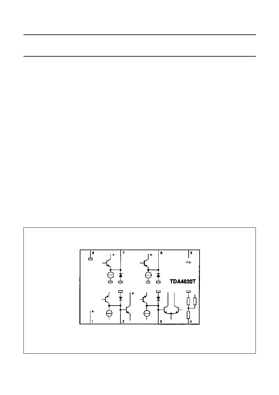
Fig.3 Internal circuits.

June 1990
5
Philips Semiconductors
Preliminary specification
Sync separation circuit for video applications
TDA4820T
LIMITING VALUES
In accordance with the Absolute Maximum System (IEC 134)
SYMBOL
PARAMETER
MIN.
MAX.
UNIT
V
P
supply voltage (pin 1)
0
13.2
V
V
i
input voltage (pin 2)
-
0.5
6
V
I
o
output current (pin 6 and pin 7)
3
-
10
mA
T
stg
storage temperature range
-
25
+
150
∞
C
T
amb
operating ambient temperature range
0
+
70
∞
C
T
j
maximum junction temperature
-
150
∞
C
P
tot
total power dissipation
-
500
mW