 | –≠–ª–µ–∫—Ç—Ä–æ–Ω–Ω—ã–π –∫–æ–º–ø–æ–Ω–µ–Ω—Ç: TDA4885 | –°–∫–∞—á–∞—Ç—å:  PDF PDF  ZIP ZIP |

DATA SHEET
Product specification
Supersedes data of 1997 Mar 19
File under Integrated Circuits, IC02
1997 Nov 25
INTEGRATED CIRCUITS
TDA4885
150 MHz video controller with
I
2
C-bus

1997 Nov 25
2
Philips Semiconductors
Product specification
150 MHz video controller with I
2
C-bus
TDA4885
CONTENTS
1
FEATURES
2
GENERAL DESCRIPTION
3
ORDERING INFORMATION
4
QUICK REFERENCE DATA
5
BLOCK DIAGRAM
6
PINNING
7
FUNCTIONAL DESCRIPTION
7.1
Signal input stage
(input clamping, blanking and clipping)
7.2
Electronic potentiometer stages
7.2.1
Contrast control (driven by I
2
C-bus, 6-bit DAC)
7.2.2
Brightness control (driven by I
2
C-bus, 6-bit
DAC)
7.2.3
Gain control (driven by I
2
C-bus, 6-bit DAC) and
grey scale tracking
7.3
Output stage
7.4
Pedestal blanking
7.5
Output clamping, feedback references and
DAC outputs
7.6
Clamping and blanking pulses
7.7
On Screen Display (OSD)
7.8
Limiting by contrast reduction
7.9
Gain modulation
7.10
I
2
C-bus control
8
LIMITING VALUES
9
THERMAL CHARACTERISTICS
10
CHARACTERISTICS
11
I
2
C-BUS PROTOCOL
12
INTERNAL CIRCUITRY
13
TEST AND APPLICATION INFORMATION
13.1
Test application
13.2
Recommendations for building the application
board
14
PACKAGE OUTLINE
15
SOLDERING
15.1
Introduction
15.2
Soldering by dipping or by wave
15.3
Repairing soldered joints
16
DEFINITIONS
17
LIFE SUPPORT APPLICATIONS
18
PURCHASE OF PHILIPS I
2
C COMPONENTS

1997 Nov 25
3
Philips Semiconductors
Product specification
150 MHz video controller with I
2
C-bus
TDA4885
1
FEATURES
∑
150 MHz pixel rate
∑
2.7 ns rise time
∑
Gain modulation capability for brightness uniformity
∑
I
2
C-bus control
∑
Grey scale tracking
∑
On Screen Display (OSD) mixing
∑
Negative feedback for DC-coupled cathodes
∑
Positive feedback for AC-coupled cathodes
∑
DAC outputs for black level restoration with AC-coupled
cathodes
∑
Integrated black level storage capacitors
∑
Beam current limiting
∑
Analog subcontrast setting
∑
Pedestal blanking
∑
OSD contrast
∑
Sync clipping.
2
GENERAL DESCRIPTION
The TDA4885 is a monolithic integrated RGB pre-amplifier
for colour monitor systems (e.g. 15" and 17") with I
2
C-bus
control and OSD. In addition to bus control beam current
limiting and gain modulation are possible. The signals are
amplified in order to drive commonly used video modules
or discrete solutions. Individual black level control with
negative feedback from the cathode (DC coupling) or fixed
black level control with positive feedback and 3 DAC
outputs for external cut-off control (AC coupling) is
possible.
With special advantages the circuit can be used in
conjunction with the TDA485x monitor deflection IC family.
3
ORDERING INFORMATION
TYPE
NUMBER
PACKAGE
NAME
DESCRIPTION
VERSION
TDA4885
SDIP32
plastic shrink dual in-line package; 32 leads (400 mil)
SOT232-1

1997 Nov 25
4
Philips Semiconductors
Product specification
150 MHz video controller with I
2
C-bus
TDA4885
4
QUICK REFERENCE DATA
SYMBOL
PARAMETER
CONDITIONS
MIN.
TYP.
MAX. UNIT
V
P
supply voltage (pin 7)
7.6
8.0
8.8
V
I
P
supply current (pin 7)
-
20
25
mA
V
P1, 2, 3
channel supply voltage
(pins 29, 24 and 19)
7.6
8.0
8.8
V
I
P1, 2, 3
channel supply current
(pins 29, 24 and 19)
-
40
-
mA
V
i(b-w)
input voltage
(black-to-white value; pins 6, 8 and 10)
-
0.7
1.0
V
V
o(b-w)
nominal output voltage swing
(black-to-white value; pins 30, 25 and 20)
nominal contrast;
maximum gain; pins 12,
13 and 14 grounded
2.5
2.8
-
V
V
o(b-w)(max)
maximum output voltage swing
(black-to-white value; pins 30, 25 and 20)
maximum contrast;
maximum gain; pins 12,
13 and 14 grounded
-
4.5
-
V
V
o
output voltage level (pins 30, 25 and 20)
0.1
-
6.0
V
V
bl
typical reference black level
(pins 30, 25 and 20)
0.5
-
2.5
V
I
o(sink)
peak output sink current
during fast signal transients
-
-
20
mA
I
o(source)
peak output source current
during fast signal transients
-
40
-
-
mA
B
bandwidth
-
3 dB (small signal)
-
150
-
MHz
t
r(O)
video rise time at signal outputs
(pins 30, 25 and 20)
-
2.7
-
ns
dV
O
over/undershoot at signal outputs
(pins 30, 25 and 20)
minimum rise/fall time
-
5
-
%
ct
crosstalk at signal outputs
(pins 30, 25 and 20)
f = 80 MHz
-
-
30
-
dB
C
C
contrast control related to nominal contrast
-
28
-
+4
dB
G
C
gain control related to maximum gain
-
7
-
0
dB
BC
brightness control (typical black level voltage
change related to output signal amplitude)
-
10
-
+30
%
V
o(OSD)(max)
maximum OSD output voltage swing related
to nominal output voltage swing
(pins 30, 25 and 20)
maximum OSD contrast;
maximum gain; pins 12,
13 and 14 grounded
-
125
-
%
C
OSD
OSD contrast control related to maximum
OSD contrast
-
12
-
0
dB

1997 Nov 25
5
Philips Semiconductors
Product specification
150 MHz video controller with I
2
C-bus
TDA4885
5
BLOCK DIAGRAM
Fig.1 Block diagram.
ok, full pagewidth
MHA343
INPUT-
CLAMPING
BLANKING
CLIPPING
INPUT-
CLAMPING
BLANKING
CLIPPING
INPUT-
CLAMPING
BLANKING
CLIPPING
LIMITING
CONTRAST
TDA4885
V
I1
V
I2
V
I3
OSD-
CONTRAST
PEDST
DISO
DISV
FPOL
data
CONTRAST
CONTRAST
DISO
1234
51
1
79
FBL
OSD
1
OSD
2
OSD
3
fast blanking
blanking
input clamping
OSD-INPUT
INPUT CLAMPING
VERTICAL BLANKING
BLANKING
OUTPUT CLAMPING
6-BIT
DAC
I
2
C-BUS
REGISTER
BLANKING
MODULATION
FPOL
POLARITY
SWITCH
PEDESTAL
BLANKING
PEDESTAL
BLANKING
PEDESTAL
BLANKING
BRIGHTNESS
GAIN
GAIN
PEDST
PEDST
PEDST
HFB
CLI
GND
DISV
GAIN
BRIGHTNESS
BRIGHTNESS
SUPPLY
4-BIT
DAC
6-BIT
DAC
6-BIT
DAC
6-BIT
DAC
6-BIT
DAC
8-BIT
DAC
8-BIT
DAC
8-BIT
DAC
CHANNEL 3
REFERENCE
CHANNEL 2
REFERENCE
CHANNEL 1
REFERENCE
OSD-
CONTRAST
OSD-
CONTRAST
signal path 1
signal path 2
signal path 3
6
17
15
16
LIM
SDA
SCL
12
GM
1
GM
2
GM
3
13
14
8
10
22
REF
3
REF
2
REF
1
V
P1
V
O1
GND
1
FB
1
V
P2
V
O2
FB
2
V
P3
V
O3
GND
3
GND
2
FB
3
V
P
27
32
29
30
28
31
24
25
23
26
19
20
18
21

1997 Nov 25
6
Philips Semiconductors
Product specification
150 MHz video controller with I
2
C-bus
TDA4885
6
PINNING
SYMBOL
PIN
DESCRIPTION
FBL
1
fast blanking input for OSD insertion
OSD
1
2
OSD input channel 1
OSD
2
3
OSD input channel 2
OSD
3
4
OSD input channel 3
CLI
5
vertical blanking input
(input clamping)
V
I1
6
signal input channel 1
V
P
7
supply voltage
V
I2
8
signal input channel 2
GND
9
ground
V
I3
10
signal input channel 3
HFB
11
horizontal flyback input
(output clamping, blanking)
GM
1
12
gain modulation input channel 1
GM
2
13
gain modulation input channel 2
GM
3
14
gain modulation input channel 3
SDA
15
I
2
C-bus serial data input/output
SCL
16
I
2
C-bus clock input
LIM
17
beam current limiting input,
subcontrast setting
GND
3
18
ground channel 3
V
P3
19
supply voltage channel 3
V
O3
20
signal output channel 3
FB
3
21
feedback input channel 3
REF
3
22
reference voltage channel 3
GND
2
23
ground channel 2
V
P2
24
supply voltage channel 2
V
O2
25
signal output channel 2
FB
2
26
feedback input channel 2
REF
2
27
reference voltage channel 2
GND
1
28
ground channel 1
V
P1
29
supply voltage channel 1
V
O1
30
signal output channel 1
FB
1
31
feedback input channel 1
REF
1
32
reference voltage channel 1
Fig.2 Pin configuration.
handbook, halfpage
TDA4885
MHA342
1
2
3
4
5
6
7
8
9
10
11
12
13
14
15
16
32
31
30
29
28
27
26
25
24
23
22
21
20
19
18
17
FBL
OSD1
OSD2
OSD3
CLI
VI1
VP
VI2
GND
VI3
HFB
GM1
GM2
GM3
REF1
FB1
VO1
VP1
REF2
FB2
GND1
VO2
VP2
GND2
REF3
FB3
VO3
VP3
SDA
SCL
GND3
LIM

1997 Nov 25
7
Philips Semiconductors
Product specification
150 MHz video controller with I
2
C-bus
TDA4885
7
FUNCTIONAL DESCRIPTION
See block diagram (Fig.1) and definition of levels and
output signals (Chapter "Characteristics" notes 1 to 3;
Figs 3 to 6).
7.1
Signal input stage
(input clamping, blanking and clipping)
The RGB input signals with nominal signal amplitude of
0.7V
b-w
are capacitively coupled into the TDA4885 from a
low-ohmic source (75
recommended) and actively
clamped to an internal DC voltage during signal black
level. Because of the high-ohmic input impedance of the
TDA4885 the coupling capacitor (which also functions as
storage capacitor during clamping pulses) can be
relatively small (10 nF recommended). The internal
leakage currents will discharge the coupling capacitor
resulting in black output signals for missing input
clamping pulses.
Composite signals will not disturb normal operations
because a clipping circuit cuts all signal parts below
black level.
A fast signal blanking stage belongs to the input stage
which is driven by several blanking pulses (see Section
"Clamping and blanking pulses") and control bit DISV = 1.
During the off condition the internal reference black level
will be inserted instead of the input signals.
7.2
Electronic potentiometer stages
7.2.1
C
ONTRAST CONTROL
(
DRIVEN BY
I
2
C-
BUS
, 6-
BIT
DAC)
The input signals related to the internal reference black
level can be simultaneously adjusted by contrast control
with a control range of typically 32 dB. The nominal
contrast setting is defined for 26H (4 dB below maximum).
7.2.2
B
RIGHTNESS CONTROL
(
DRIVEN BY
I
2
C-
BUS
, 6-
BIT
DAC)
With brightness control the video black level will be shifted
in relation to the reference black level simultaneously for
all three channels. With a negative setting (maximum 10%
of nominal signal amplitude) dark signal parts will be lost in
ultra black while for positive settings (maximum 30% of
nominal signal amplitude) the background will alter from
black to grey. The nominal brightness setting (10H) is no
shift. The brightness setting is also valid for OSD signals.
During blanking and output clamping the video black level
will be blanked to reference black level (brightness
blanking).
7.2.3
G
AIN CONTROL
(
DRIVEN BY
I
2
C-
BUS
, 6-
BIT
DAC)
AND GREY SCALE TRACKING
Gain control is used for white point adjustment (correction
for different voltage to light amplification of the three colour
channels) and therefore individual for the three channels.
The video signals related to the reference black level can
be gain controlled within a range of typical 7 dB.
The nominal setting is maximum gain. The video signal is
the addition of the contrast controlled input signal and the
brightness shift. The gain setting is also valid for OSD
signals, thus the complete `grey scale' is effected by gain
control.
7.3
Output stage
In the output stage the nominal input signal will be
amplified to 2.8V
b-w
output colour signal at nominal
contrast and maximum gain. The maximum input-output
amplification at maximum contrast and gain settings is
16 dB. By output clamping the reference black level can
be adjusted. In order to achieve very fast rise and fall times
of the output signals with minimum crosstalk between the
channels, each output stage has its own supply voltage
and ground pin.
7.4
Pedestal blanking
For the video portion the reference black level should
correspond to the `extended cut-off voltage' at the
cathode. During vertical flyback nevertheless retrace lines
may be visible, though blanking to spot cut-off is useful.
With control bit PEDST = 1 the pedestal black level will be
adjusted by output clamping instead of the reference black
level (see Fig.5). The pedestal black level is more negative
than the video black level at minimum brightness setting
and the voltage difference to reference black level is
independent of any user control.
7.5
Output clamping, feedback references and
DAC outputs
Aim of the output clamping (pins FB
1
, FB
2
and FB
3
) is to
set the reference black level of the signal outputs to a
value which corresponds to the `extended cut-off voltage'
of the CRT cathodes. At lack of output clamping pulses the
integrated storage capacitors will discharge resulting in
output signals going to switch-off voltage. Feedback
references are driven by the I
2
C-bus.

1997 Nov 25
8
Philips Semiconductors
Product specification
150 MHz video controller with I
2
C-bus
TDA4885
1. Control bit FPOL = 0
The cathode voltage (DC-coupled) is divided by a
voltage divider and fed back to the IC. During the
output clamping pulse it is compared with an
adjustable feedback reference voltage with a range of
5.8 to 4.0 V. Any difference will lead to a reference
black level correction (control bit PEDST = 0) or
pedestal black level correction (control bit PEDST = 1)
by charging or discharging the integrated capacitor
which stores the black level information between the
output clamping pulses. The DC voltages of the output
stages should be designed in such a way that the
reference black level/pedestal black level is within the
range of 0.5 to 2.5 V. The reference voltages are also
fed to the DAC output pins (REF
1
, REF
2
and REF
3
).
For correct operation it is necessary that there is
enough room for ultra black signals (negative
brightness setting, pedestal black level if control bit
PEDST = 1). Any clipping with the video supply
voltage can disturb signal rise/fall times or the black
level stabilization.
2. Control bit FPOL = 1
For applications with AC-coupled cathodes positive
feedback can be taken directly or divided by a voltage
divider from the signal outputs or the emitter of an
external emitter follower. During the output clamping
pulse it is compared with a fixed reference voltage of
0.7 V.
For black level restoration the DAC outputs (REF
1
,
REF
2
and REF
3
) with a range of 5.8 to 4.0 V can be
used.
The use of pedestal blanking allows a very simple
black level restoration with a DC diode clamp instead
of a complicated pulse restoration circuit because the
pedestal black level is the most negative output signal.
7.6
Clamping and blanking pulses
The pin CLI of TDA4885 can be directly connected to
pin CLBL of e.g. TDA4855 sync processor for input
clamping pulses and vertical blanking pulses.
The threshold for the input clamping pulse (typical 3 V) is
higher than the threshold for the vertical blanking pulse
(typical 1.4 V) but there must be no blanking during input
clamping. Thus vertical blanking only is enabled if no input
clamping is detected. For this reason the input clamping
pulse must have rise/fall times faster than 75 ns/V during
the transition from 1.2 to 3.5 V and opposite. The internal
vertical blanking pulse will be delayed by typical 290 ns.
During the vertical blanking pulse at pin CLI signal
blanking, brightness blanking and with control bit
PEDST = 1 pedestal blanking will be activated. Input
clamping pulses during vertical blanking will not switch off
blanking.
For proper input clamping the input signals have to be at
black level during the input clamping pulse.
An input pulse at pin HFB (e.g. horizontal flyback pulse)
will be scanned with two thresholds. If the input pulse
exceeds the first one (typical 1.4 V) signal blanking,
brightness blanking and if control bit PEDST = 1
pedestal blanking will be activated. If the input pulse
exceeds the second one (typical 3 V) additionally output
clamping will be activated. The vertical blanking pulse can
also be mixed with the horizontal flyback pulse at pin HFB.
7.7
On Screen Display (OSD)
If the fast blanking input signal at pin FBL exceeds the
threshold (typical 1.4 V) the input signals are blanked
(signal blanking) and OSD signals are enabled. Then any
signal at pins OSD
1
, OSD
2
or OSD
3
exceeding the same
threshold will create an insertion signal with an amplitude
of 125% of the nominal colour signal (approximately 80%
of the maximum colour signal). The amplitude can be
controlled by OSD contrast (driven by I
2
C-bus) with a
range of 12 dB. The OSD signals are inserted at the same
point as the contrast controlled input signals and will be
treated with brightness and gain control like normal input
signals.
With control bit DISO = 1 OSD, signal insertion and fast
blanking (pin FBL) are disabled.
7.8
Limiting by contrast reduction
Beam current limiting is possible with an external voltage
at pin LIM. The maximum overall voltage gain of contrast
(and OSD contrast) control can be reduced by a voltage
between 4.5 V (start of reduction) and 2.0 V (
-
26 dB)
without effecting the contrast bit resolution. By setting the
maximum voltage at pin LIM to less than 4.5 V the
maximum gain is reduced for all channels (subcontrast
setting). The open-circuit pin will have a voltage of
approximately 5.0 V but is very high-ohmic and should be
tied to a voltage source of 5.0 V or higher or should be
connected to a capacitance of some nF if not used.

1997 Nov 25
9
Philips Semiconductors
Product specification
150 MHz video controller with I
2
C-bus
TDA4885
7.9
Gain modulation
To achieve brightness uniformity over the screen scan
dependent gain modulation is possible. With open-circuit
pins the gain will be reduced by 20% giving the possibility
of symmetrical gain modulations (
±
18%) with
±
1 V related
to the open-circuit voltage of about 2.0 V at any gain
setting.
If the gain modulation feature will not be used pins GM
1
,
GM
2
and GM
3
should be grounded to profit by maximum
voltage gain.
7.10
I
2
C-bus control
The TDA4885 contains an I
2
C-bus receiver for several
control functions:
1. Contrast control with 6-bit DAC
2. Brightness control with 6-bit DAC
3. OSD contrast control with 4-bit DAC
4. Gain control for each channel with 6-bit DAC
5. Internal feedback reference and external reference
voltage control for each channel with 8-bit DAC
6. Control register with control bits FPOL, DISV, DISO
and PEDST
7. Test register for production tests only.
All registers are set to logic 0 (minimum value for control
registers) after power-up and after internal power-on reset
of the I
2
C-bus.

1997 Nov 25
10
Philips Semiconductors
Product specification
150 MHz video controller with I
2
C-bus
TDA4885
8
LIMITING VALUES
In accordance with the Absolute Maximum Rating System (IEC 134).
Notes
1. No external voltages.
2. Equivalent to discharging a 200 pF capacitor via a 10
series resistor (
"UZW-B0/FQ-B302").
3. Equivalent to discharging a 100 pF capacitor via a 1500
series resistor (
"UZW-B0/FQ-A302").
9
THERMAL CHARACTERISTICS
SYMBOL
PARAMETER
MIN.
MAX.
UNIT
V
P
supply voltage (pin 7)
0
8.8
V
V
P1, 2, 3
supply voltage channel 1, 2 and 3 (pins 29, 24 and 19) 0
8.8
V
V
i
input voltage (pins 6, 8 and 10)
-
0.1
V
P
V
V
ext
external DC voltage applied to the following pins:
pins 1 to 4
-
0.1
V
P
V
pins 12, 13, 14 and 17
-
0.1
V
P
V
pins 11 and 5
-
0.1
V
P
+ 0.7
V
pins 15 and 16
-
0.1
V
P
V
pins 31, 26 and 21
-
0.1
V
P
+ 0.7
V
pins 30, 25 and 20
note 1
note 1
pins 32, 27 and 22
-
0.1
V
P
V
I
o(av)
average output current (pins 30, 25 and 20)
-
20
mA
I
OM
peak output current (pins 30, 25 and 20)
-
50
mA
P
tot
total power dissipation
-
1300
mW
T
stg
storage temperature
-
25
+150
∞
C
T
amb
operating ambient temperature
-
20
+70
∞
C
T
j
junction temperature
-
25
+150
∞
C
V
ESD
electrostatic handling for all pins
machine model 0.75
µ
H (note 2)
-
250
+250
V
human body model (note 3)
-
3000
+3000
V
SYMBOL
PARAMETER
CONDITIONS
VALUE
UNIT
R
th(j-a)
thermal resistance from junction to ambient
in free air
60
K/W

1997 Nov 25
11
Philips Semiconductors
Product specification
150 MHz video controller with I
2
C-bus
TDA4885
10 CHARACTERISTICS
All voltages and currents are measured in test circuit of Fig.19; all voltages are measured with respect to GND (pins 9,
28, 23 and 18); V
P
= V
P1, 2, 3
= 8 V (pins 7, 29, 24 and 19); T
amb
= 25
∞
C; nominal input signals [0.7 V (peak-to-peak
value) at pins 6, 8 and 10]; nominal colour signals at signal outputs (pins 30, 25 and 20); reference black level (V
rbl
)
approximately 0.7 V; nominal settings for brightness and contrast; maximum settings for OSD contrast and gain; no
limiting of contrast (V
17
= 5 V); no OSD fast blanking (pin 1 connected to ground); no gain modulation (pins 12, 13
and 14 connected to ground); notes 1 to 3; unless otherwise specified.
SYMBOL
PARAMETER
CONDITIONS
MIN.
TYP.
MAX.
UNIT
Supply
V
P
supply voltage (pin 7)
7.6
8.0
8.8
V
I
P
supply current (pin 7)
note 4
-
20
25
mA
V
P1, 2, 3
channel supply voltage
(pins 29, 24 and 19)
7.6
8.0
8.8
V
I
P1, 2, 3
channel supply current
(pins 29, 24 and 19)
signal outputs (pins 30, 25
and 20) open-circuit;
V
rbl
= 0.7 V; note 5
-
40
45
mA
V
PSO
supply voltage for signal switch
off (threshold at pin 7)
signal outputs switched to
switch-off voltage; note 1
-
-
7.2
V
Clamping and blanking pulses (pins 5 and 11)
V
5
input clamping and vertical
blanking input signal
note 6
no blanking, no input
clamping
-
0.1
-
+1.2
V
blanking, no input clamping
1.6
-
2.6
V
input clamping, no blanking
3.5
-
V
P
V
I
5
input current
V
5
= 1 V; note 7
-
1.5
-
0.2
-
0.05
µ
A
pin 5 grounded; note 7
-
80
-
60
-
30
µ
A
V
5
=
-
0.1 V; note 7
-
250
-
200
-
100
µ
A
t
r/f5
rise/fall time for input clamping
pulse, disable for blanking
note 6; see Fig.7
-
-
75
ns/V
t
W5
width of input clamping pulse
0.6
-
-
µ
s
t
dl5
delay between leading edges
of vertical blanking input pulse
and internal blanking pulse
V
11
< 0.8 V; input pulse with
50 ns/V; threshold for rising
input pulse V
5
= 1.4 V;
threshold after input clamping
pulse V
5
= 3 V; see Fig.7
-
270
-
ns
t
dt5
delay between trailing edges of
vertical blanking input pulse
and internal blanking pulse
V
11
< 0.8 V; input pulse with
50 ns/V; threshold V
5
= 1.4 V;
see Fig.7
-
115
-
ns
V
11
output clamping and blanking
input signal
note 8
no blanking, no output
clamping
-
0.1
-
+0.8
V
blanking, no output clamping
2.0
-
2.6
V
blanking, output clamping
3.5
-
V
P
V
1997 Nov 25
12
Philips Semiconductors
Product specification
150 MHz video controller with I
2
C-bus
TDA4885
I
11
input current
V
11
= 0.8 V; note 7
-
3
-
0.4
-
0.1
µ
A
pin 5 grounded; note 7
-
80
-
60
-
30
µ
A
V
5
=
-
0.1 V; note 7
-
250
-
200
-
100
µ
A
Video signal inputs (channel 1: pin 6; channel 2: pin 8; channel 3: pin 10)
V
i(b-w)6, 8, 10
positive input signal referred to
black
-
0.7
1.0
V
V
I(clamp)6, 8, 10
DC voltage during input
clamping
note 9
-
4
-
V
I
I6, 8, 10
DC input current
no input clamping;
V
I6, 8, 10
= V
I(clamp)6, 8, 10
;
T
amb
=
-
20 to +70
∞
C
0.02
0.20
0.35
µ
A
during input clamping;
V
I6, 8, 10
= V
I(clamp)6, 8, 10
±
0.7 V
±
110
±
150
±
190
µ
A
Z
i6, 8, 10
magnitude of signal input
impedance
f = 100 MHz;
V
I(DC)6, 8, 10
= V
I(clamp)6, 8, 10
500
-
-
C
i6, 8, 10
input capacitance against
ground
-
-
3
pF
Signal blanking
ct(bl)
crosstalk suppression from
input to output during blanking
control bit DISV = 1; f = 80 MHz 20
30
-
dB
control bit DISV = 1;
f = 135 MHz
10
15
-
dB
t
d11(sig)l
delay between blanking input
(leading edge) and output
signal blanking
see Fig.8
-
55
-
ns
t
d11(sig)t
delay between blanking input
(trailing edge) and output
signal blanking
see Fig.8
-
25
-
ns
Clipping (measured at signal outputs)
V
clipp
offset during sync clipping
related to nominal colour signal
V
I6, 8, 10
= V
I(clamp)6, 8, 10
;
note 10; see Fig.3
-
1
2
%
Contrast control; see Fig.9 and note 11
d
C
colour signal related to nominal
colour signal
3FH (maximum)
-
4
-
dB
26H (nominal)
-
0
-
dB
00H (minimum)
-
-
28
-
dB
G
track
tracking of output colour
signals of channels 1, 2 and 3
3FH to 00H; note 12
-
0.0
0.5
dB
SYMBOL
PARAMETER
CONDITIONS
MIN.
TYP.
MAX.
UNIT

1997 Nov 25
13
Philips Semiconductors
Product specification
150 MHz video controller with I
2
C-bus
TDA4885
Fast blanking (pin 1) and OSD signal insertion (channel 1: pin 2; channel 2: pin 3; channel 3: pin 4); note 13
V
1
fast blanking input signal
no video signal blanking, OSD
signal insertion disabled
0
-
1.1
V
video signal blanking, OSD
signal insertion enabled
1.7
-
V
P
-
1
V
V
2, 3, 4
OSD input signal
V
1
> 1.7 V
no internal OSD signal
insertion
0
-
1.1
V
internal OSD signal insertion
1.7
-
V
P
-
1
V
t
f(FBL)
fall time of colour signals
(pins 30, 25 and 20)
90 to 10% amplitude; start of
fast blanking pulse at pin 1 with
1.2 ns/V; note 14; see Fig.10
-
-
10
ns
t
r(FBL)
rise time of colour signals
(pins 30, 25 and 20)
10 to 90% amplitude; end of
fast blanking pulse at pin 1 with
1.2 ns/V; note 14; see Fig.10
-
-
10
ns
t
r(OSD)
rise time of OSD colour signals 10 to 90% amplitude; input
pulse with 1.2 ns/V; see Fig.10
-
-
4
ns
t
f(OSD)
fall time of OSD colour signals
90 to 10% amplitude; input
pulse with 1.2 ns/V; see Fig.10
-
-
7
ns
t
g(CO)
width of (negative going) OSD
signal insertion glitch, leading
edge
identical pulses with 1.2 ns/V at
fast blanking input (pin 1) and
OSD signal inputs (pins 2,
3 and 4); note 15; see Fig.10
-
-
6
ns
t
g(OC)
width of (negative going) OSD
signal insertion glitch, trailing
edge
identical pulses with 1.2 ns/V at
fast blanking input (pin 1) and
OSD signal inputs (pins 2,
3 and 4); note 15; see Fig.10
-
-
6
ns
dV
OSD
overshoot/undershoot of OSD
colour signal related to actual
OSD output pulse amplitude
OSD input pulse (pins 2, 3
and 4) with 1.2 ns/V; V
1
>
1.7 V
-
13
20
%
t
over
time of OSD signal overshoot
exceeding 10%
OSD input pulse (pins 2, 3
and 4) with 1.2 ns/V; V
1
>
1.7 V
-
-
2
ns
V
OSD(max)
maximum OSD colour signal
related to nominal colour signal
maximum OSD contrast;
maximum gain; pins 12,
13 and 14 connected to ground
100
125
150
%
OSD contrast control; see Fig.11 and note 16
d
OC
OSD colour signal related to
maximum OSD colour signal
00H (minimum)
-
14
-
12
-
10
dB
0FH (maximum)
-
0
-
dB
SYMBOL
PARAMETER
CONDITIONS
MIN.
TYP.
MAX.
UNIT

1997 Nov 25
14
Philips Semiconductors
Product specification
150 MHz video controller with I
2
C-bus
TDA4885
Limiting (pin 17); see Fig.9 and note 17
V
17(nom)
input voltage
pin 17 open-circuit
4.7
5.0
5.3
V
V
17(start)
starting voltage for contrast
and OSD contrast reduction
4.2
4.5
4.8
V
V
17(stop)
stop voltage for contrast and
OSD contrast reduction
-
32 dB below maximum colour
signal (contrast setting 3FH)
1.5
2.0
2.5
V
I
17
maximum input current
V
17
= 0 V
-
1.0
-
0.5
-
0.1
µ
A
Brightness control; see Fig.12 and notes 18 and 19
V
bl
difference between black level
and reference black level at
signal outputs related to
nominal colour signal
3FH (maximum)
+25
+30
+35
%
10H (nominal)
-
2
0
+2
%
00H (minimum)
-
12
-
10
-
8
%
V
BT
difference of
V
bl
between any
two channels related to
nominal colour signal
-
1.2
0
+1.2
%
Brightness blanking
t
d11(br)l
delay between blanking input
at pin 11 (leading edge) and
brightness blanking at signal
outputs
see Fig.8
-
-
60
ns
t
d11(br)t
delay between blanking input
at pin 11 (trailing edge) and
brightness blanking at signal
outputs
see Fig.8
-
-
60
ns
Gain control; see Fig.13 and note 20
d
G
video signal related to video
signal at maximum gain
00H (minimum)
-
8
-
7
-
6
dB
3FH (maximum)
-
0
-
dB
Gain modulation (channel 1: pin 12; channel 2: pin 13; channel 3: pin 14)
V
12, 13, 14
input voltage
symmetrical modulation
1.0
-
3.0
V
modulation feature not in use
-
-
0
V
nominal: pins 12, 13 and 14
open-circuit
1.8
2.0
2.2
V
G
mod1, 2, 3
gain modulation channels 1, 2
and 3
note 21; see Fig.14
pins 12, 13 and 14 grounded
(modulation feature not in
use)
112
120
130
%
V
12, 13, 14
= 1 V (maximum)
112
118
124
%
V
12, 13, 14
= 2 V
-
100
-
%
V
12, 13, 14
= 3 V (minimum)
76
82
88
%
SYMBOL
PARAMETER
CONDITIONS
MIN.
TYP.
MAX.
UNIT
1997 Nov 25
15
Philips Semiconductors
Product specification
150 MHz video controller with I
2
C-bus
TDA4885
Pedestal blanking
V
30, 25, 20PED
difference of pedestal black
level to video black level at
nominal brightness at signal
output pins related to nominal
colour signal
note 22; see Fig.5
-
18
-
16
-
14
%
V
30, 25, 20PED(T)
variation of
V
30, 25, 20PED
with
temperature related to nominal
colour signal
T
amb
=
-
20 to +70
∞
C
-
0.8
0
+0.8
%
Signal outputs (channel 1: pin 30; channel 2: pin 25; channel 3: pin 20)
V
30, 25, 20(b-w)
nominal colour signal
nominal contrast; maximum
gain; pins 12, 13 and 14
grounded; V
I(b-w)
= 0.7 V;
without load
2.5
2.8
3.1
V
V
30, 25, 20(max)
maximum colour signal
maximum contrast; maximum
gain; pins 12, 13 and 14
grounded; V
I(b-w)
= 0.7 V;
without load
4.0
4.5
5
V
V
30, 25, 20(min)
switch-off voltage
(minimum output voltage level)
-
0.05
0.1
V
V
30, 25, 20(max)
maximum output voltage level
at arbitrary input signals,
contrast, brightness and gain
adjustments; without load
V
P
-
2
-
V
P
-
1
V
R
30, 25, 20
output resistance
-
80
-
I
30, 25, 20
maximum source current
-
15
-
-
mA
I
30, 25, 20M(source)
peak source current
during fast positive signal
transients
-
40
-
-
mA
I
30, 25, 20M(sink)
peak sink current
during fast negative signal
transients
-
-
20
mA
S/N
signal-to-noise ratio
note 23
44
50
-
dB
D
30, 25, 20(th)
output thermal distortion
note 24
-
-
0.6
%
Frequency response at signal outputs (channel 1: pin 30; channel 2: pin 25; channel 3: pin 20)
G
30, 25, 20(f)
amplification decrease by
frequency response
f = 135 MHz (small signal)
-
1.2
3.0
dB
t
r(30, 25, 20)
rise time of fast transients
10 to 90% amplitude; nominal
colour signal; note 25
-
2.7
3
ns
t
f(30, 25, 20)
fall time of fast transients
90 to 10% amplitude; nominal
colour signal; note 25
-
3.9
4.3
ns
dV
30, 25, 20
over/undershoot of output
signal pulse related to actual
output pulse amplitude
input rise/fall time = 1 ns;
nominal colour signal
-
5
10
%
SYMBOL
PARAMETER
CONDITIONS
MIN.
TYP.
MAX.
UNIT

1997 Nov 25
16
Philips Semiconductors
Product specification
150 MHz video controller with I
2
C-bus
TDA4885
Crosstalk at signal outputs (channel 1: pin 30; channel 2: pin 25; channel 3: pin 20)
ct(tr)
transient crosstalk suppression input rise/fall time = 1 ns;
note 26
10
25
-
dB
ct(f)
crosstalk suppression by
frequency
f = 50 MHz
25
30
-
dB
f = 100 MHz
10
20
-
dB
Internal feedback reference voltage; see Fig.15 and note 27
V
ref(n)
internal reference voltage for
negative feedback polarity
FFH; FPOL = 0
3.8
4.0
4.2
V
00H; FPOL = 0
5.6
5.8
6.1
V
V
ref(p)
fixed internal reference voltage
for positive feedback polarity
FPOL = 1
0.6
0.7
0.8
V
V
ref
/
T
variation of V
ref(n)
and V
ref(p)
in
the temperature range
T
amb
=
-
20 to +70
∞
C
0
-
±
1.0
%
V
ref
/
V
P
variation of V
ref(n)
and V
ref(p)
with supply voltage V
P
7.6 V
V
P
8.8 V
0
-
±
1.0
%
External reference voltages (REF
1
: pin 32; REF
2
: pin 27; REF
3
: pin 22); see Fig.16 and note 28
V
32, 27, 22
external reference voltage
(equal to internal reference
voltage with control bit
FPOL = 0 )
FFH
3.8
4.0
4.2
V
00H
5.6
5.8
6.1
V
V
32, 27, 22
/
T
variation of V
32, 27, 22
in the
temperature range
T
amb
=
-
20 to +70
∞
C
0
-
±
1.0
%
V
32, 27, 22
/
V
P
variation of V
32, 27, 22
with
supply voltage V
P
7.6 V
V
P
8.8 V
0
-
±
1.0
%
R
32, 27, 22
output resistance
-
90
-
I
32, 27, 22
maximum sink current
-
-
400
µ
A
I
32, 27, 22
maximum source current
-
-
330
-
280
µ
A
Output clamping, feedback inputs (channel 1: pin 31; channel 2: pin 26; channel 3: pin 21)
I
31, 26, 21(max)
maximum input current
during output clamping;
V
11
> 3.5 V; V
31, 26, 21
= 0.5 V
-
500
-
100
-
60
nA
V
30, 25, 20rbl(min)
minimum reference black level
PEDST = 0; V
11
> 3.5 V
0.01
0.1
0.5
V
minimum pedestal black level
PEDST = 1; V
11
> 3.5 V
0.01
0.1
0.5
V
V
30, 25, 20rbl(max)
maximum reference black level PEDST = 0; V
11
> 3.5 V
2.4
2.8
4
V
maximum pedestal black level
PEDST = 1; V
11
> 3.5 V
2.4
2.8
4
V
V
bl(CRT)
black level variation at CRT
note 29
0
40
200
mV
V
bl(lf)
black level variation between
clamping pulses related to
nominal colour signal
line frequency 60 kHz;
10% duty cycle
-
0.1
0.5
%
t
W11
width of clamping pulse
measured at V
11
= 3 V;
see Fig.8
1
-
-
µ
s
t
d11(clamp)l
delay between clamping input
at pin 11 (leading edge) and
start of internal output clamping
pulse
see Fig.8
-
-
300
ns
SYMBOL
PARAMETER
CONDITIONS
MIN.
TYP.
MAX.
UNIT

1997 Nov 25
17
Philips Semiconductors
Product specification
150 MHz video controller with I
2
C-bus
TDA4885
Notes to the characteristics
1. Definition of levels (see Figs 3 to 5):
Reference black level: this is the level to which the input level is clamped during the input clamping pulse
(V
5
> 3.5 V). It is used internally as a reference for the gain settings. It can be observed on the outputs:
a) when the input is at black and the brightness setting is nominal (subaddress 01H = 10H)
b) during output blanking/clamping (V
11
> 3.5 V) if control bit PEDST = 0.
Video black level: this is the black level of the actual video. On the input it is still equal to the reference black level.
On the output it may deviate from it according to the brightness setting. Contrast setting leaves the video black level
unaltered .
Pedestal black level: this is an ultra black level which deviates from reference black level by a fixed amount. It can
be observed on the output during output blanking/clamping (V
11
> 3.5 V) if control bit PEDST = 1.
Switch-off voltage: this is the lowest signal voltage at outputs. The signals will be switched off by discharging the
internal black level storage capacitors if the supply voltage is less than V
PSO
.
Blanking level: this level equals reference black (control bit PEDST = 0) or pedestal black (control bit PEDST = 1).
2. Explanation to black level adjustment:
The actual blanking level on the output depends on the external feedback application. The loop will only function
correctly if it is within the control range of V
30, 25, 20rbl(min)
to V
30, 25, 20rbl(max)
. Note: changing control bit PEDST in a
given application will not affect the blanking level, but instead shifts the video (and needs re-alignment of the three
black levels).
The three reference black levels are aligned correctly when they are made equal to the `extended cut-off levels' of
the three cathodes. Full raster and spot cut-off can only be achieved by enabling the pedestal blanking or by applying
a negative pulse to grid 1.
t
d11(clamp)t
delay between clamping input
at pin 11 (trailing edge) and
end of internal output clamping
pulse
see Fig.8
-
-
60
ns
I
2
C-bus inputs (pins 15 and 16)
f
SCL
SCL clock frequency
-
-
100
kHz
V
IL
LOW-level input voltage
0.0
-
1.5
V
V
IH
HIGH-level input voltage
3.0
-
5.0
V
I
IL
LOW-level input current
V
IL
= 0 V
-
-
-
10
µ
A
I
IH
HIGH-level input current
V
IH
= 5 V
-
-
-
10
µ
A
V
OL
LOW-level output voltage
during acknowledge
0.0
-
0.4
V
I
ack
output current at pin 15 during
acknowledge
V
OL
= 0.4 V
3.0
-
5.0
mA
V
th(POR)(r)
threshold for power-on reset on rising supply voltage
-
1.5
2.0
V
falling supply voltage
-
3.5
-
V
V
th(POR)(f)
threshold for power-on reset off rising supply voltage
-
-
7.0
V
falling supply voltage
-
1.5
-
V
SYMBOL
PARAMETER
CONDITIONS
MIN.
TYP.
MAX.
UNIT

1997 Nov 25
18
Philips Semiconductors
Product specification
150 MHz video controller with I
2
C-bus
TDA4885
3. Definition of output signals (see Fig.6):
Colour signal: all positive voltages referred to black level at signal outputs.
Nominal colour signal: colour signal with nominal input signal (0.7V
b-w
), nominal contrast setting and maximum
gain setting.
Video signal: all positive voltages referred to reference black level at signal outputs. The video signal is the
superposing of the brightness information (
V
bl
) and the colour signal.
4. The total supply current I
P
= I
7
+ I
29
+ I
24
+ I
19
depends on the supply voltage with a factor of approximately 10 mA/V
and varies in the temperature range of
-
20 to +70
∞
C by approximately
±
10% (V
30, 25, 20
= 0.7 V).
5. The channel supply current depends on the signal output current, the channel supply voltage and the signal output
voltage. With I
px
= I
29, 24, 19
at V
P1, 2, 3
= 8 V and V
30, 25, 20
= 0.7 V:
6. Pin 5 should be used for input clamping and blanking during vertical retrace (signal blanking, brightness blanking and
if control bit PEDST = 1 pedestal blanking). With a fast clamping pulse (transition between V
5
= 1.2 to 3.5 V and vice
versa in less than 75 ns/V) no blanking will occur during input clamping.
For 75 ns/V < t
r/f5
280 ns/V the generation of the internal vertical blanking pulse is uncertain, for t
r/f5
> 280 ns/V the
internal blanking pulse will be generated.
Pin 5 open-circuited will activate permanent input clamping and undefined blanking.
7. Input voltages less than
-
0.1 V can produce internal substrate currents which disturb the leakage currents at the
signal inputs. An internal protection circuit creates a current for pin voltages of approximately 0 V or less. Feeding
clamping/blanking pulses via a resistor of some k
protects the pin from negative voltages.
8. Pin 11 should be used for output clamping and/or blanking. Pin 11 open-circuited will activate permanent blanking
and output clamping.
9. The DC voltage during input clamping is temperature dependent with a factor of approximately 0.5 V/100
∞
C (3V
BE
).
10. Composite signals will not disturb normal operations because an internal clipping circuit cuts all signal parts below
input reference black level (see Fig.3).
11. Contrast control acts on internal colour signals under I
2
C-bus control; subaddress 02H
(bit resolution 1.6% of contrast range).
12.
dB
A
x
: colour signal output amplitude in channel x at any contrast setting.
A
x0
: colour signal output amplitude in channel x at nominal contrast and same gain setting.
13. When OSD fast blanking is active and V
2, 3, 4
are HIGH (V
1
> 1.7 V, V
2, 3, 4
> 1.7 V) the OSD colour signals will be
inserted in front of the gain potentiometers. This assures a correct grey scale of all video signals. The amplitudes of
the inserted OSD signals can be controlled simultaneously by OSD contrast via I
2
C-bus.
14. Typical pulse at fast blanking input (pin 1) and response at signal outputs (pins 30, 25 and 20) with nominal input
signals at pins 6, 8 and 10.
15. Typical pulse at fast blanking input (pin 1) as well as OSD inputs (pins 2, 3 and 4) and response at signal outputs
(pins 30, 25 and 20) during OSD fast blanking for maximum OSD contrast, maximum gain adjustment and pins 12,
13 and 14 grounded. Small internal threshold and delay differences between fast blanking and signal insertion might
cause short signal distortion at begin and end of signal insertion (see Fig.10).
16. OSD contrast control acts on inserted OSD colour signals under I
2
C-bus control; subaddress 03H
(bit resolution 6.7% of OSD contrast range).
I
29, 24, 19
I
px
I
30, 25, 20
3.1
mA
V
---------
V
P1, 2, 3
8 V
≠
(
)
◊
2.5
mA
V
---------
V
30 25 20
,
,
0.7 V
≠
(
)
◊
≠
+
+
G
track
20
maximum of
A
1
A
10
---------
A
20
A
2
---------
◊
log
A
1
A
10
---------
A
30
A
3
---------
◊
log
A
2
A
20
---------
A
30
A
3
---------
◊
log
;
;
◊
=

1997 Nov 25
19
Philips Semiconductors
Product specification
150 MHz video controller with I
2
C-bus
TDA4885
17. This pin can be used for beam current limiting or subcontrast setting. Both the video and OSD contrast are reduced
simultaneously (see Figs 9 and 11). Because of the high-ohmic input impedance the pin should be tied to a voltage
of more than 5 V or applied with a capacitor of some nF if not used.
18. Brightness control adds an I
2
C-bus controlled DC offset to the internal colour signal; subaddress 01H
(bit resolution 1.6% of brightness range).
19. The voltage difference between video black level and reference black level is related to the colour signal with nominal
0.7 V (peak-to-peak value) input signal, at nominal contrast (subaddress 02H = 26H) and for any gain setting.
The voltage difference is proportional to the gain setting (grey scale tracking). The given values of
V
bl
are valid only
for video black levels higher than the signal output switch-off voltage V
30, 25, 20(min)
.
20. Gain control acts on video signals and inserted OSD video signals under I
2
C-bus control; subaddress 04H
(channel 1), 05H (channel 2) and 06H (channel 3; bit resolution 1.6% of gain range).
21. The usage of the gain modulation capability results in a reduction of the overall voltage gain of the TDA4885 but gives
enough room for positive and negative modulation. Only pins 12, 13 and 14 connected to ground makes it possible
to reach the specified maximum video signals at pins 30, 25 and 20 (see Fig.14). By short-circuiting pins 12, 13 and
14 it is possible to assure that the relations between the video signals remain constant for any modulation (common
gain modulation).
22. Pedestal blanking produces an ultra black level during blanking and output clamping which is the most negative
signal at the signal output pins. The reference black level which should correspond to the `extended cut-off voltage'
at the cathodes is about
V
30, 25, 20PED
higher (see Fig.5).
The use of pedestal blanking with AC-coupled cathodes (control bit FPOL = 1) allows a very simple black level
restoration with a DC diode clamp instead of a complicated pulse restoration circuit.
23. The signal-to-noise ratio is calculated by the formula (range 1 to 135 MHz):
dB
24. There might be short time smearing effects which have no thermal causes. The final amplitude will be reached some
10 ns after pulse step (amplitude differences of about 5%). For compensation methods see Section
"Recommendations for building the application board" in Chapter "Test and application information".
25. Ideal input rise/fall time of 0 ns;
26. Crosstalk between any two output pins:
a) Input conditions: any channel (channel A) with nominal input signal and 1 ns rise time. The inputs of the other
two channels are capacitively coupled to ground (channel B). Gain setting to maximum (3FH). Contrast setting to
nominal (26H)
b) Output conditions: black level set to 1 V for each channel at signal outputs. Output signals are V
A
and V
B
respectively
c) Transient crosstalk suppression:
dB
27. Internal feedback reference voltage acts under I
2
C-bus control for control bit FPOL = 0; subaddress 07H (channel 1),
08H (channel 2) and 09H (channel 3; bit resolution 0.4% of voltage range). The internal feedback reference voltages
can be measured at feedback inputs (pins 31, 26 and 21) during output clamping (V
11
> 3.5 V) in closed feedback
loop. The feedback loop remains operative at output levels between typically 0.1 to 2.8 V. The reference voltages
are not influenced by the value of control bit PEDST. The levels of the internal feedback reference voltages depend
on the individual adjustments via I
2
C-bus (values from 00H to FFH) and the selected feedback polarity (control bit
FPOL = 0 or 1):
a) Control bit FPOL = 0: rising values of the data bytes (subaddresses 07H, 08H and 09H), e.g. 00H to FFH,
correspond to rising values of the resulting reference black levels at signal outputs (pins 30, 25 and 20)
b) Control bit FPOL = 1: the internal feedback reference voltage remains constant.
S
N
----
20
peak-to-peak value of the nominal signal output voltage
RMS value of the noise output voltage
---------------------------------------------------------------------------------------------------------------------------------------------------
log
◊
=
t
r, out
2
t
r, ideal
2
t
r, in
2
+
=
ct(tr)
20
V
A
V
B
-------
log
◊
=

1997 Nov 25
20
Philips Semiconductors
Product specification
150 MHz video controller with I
2
C-bus
TDA4885
28. The external reference voltages act under I
2
C-bus control independent from control bit FPOL; subaddress 07H
(REF
1
), 08H (REF
2
) and 09H (REF
3
; bit resolution 0.4% of voltage range).
29. Slow variations of video supply voltage V
CRT
will be suppressed at CRT cathode by the clamping feedback loop.
A change of V
CRT
with 5 V leads to a specified change of the cathode voltage.
Fig.3 Input signals.
The input video signals have to be on black level during input clamping.
handbook, full pagewidth
MHA344
input video signal
with syncs
at pins 6, 8 and 10
input clamping pulses
at pin 5
blanking/output
clamping pulses
at pin 11
input reference
black level
the syncs will be clipped
to reference black level
internally
input signals

1997 Nov 25
21
Philips Semiconductors
Product specification
150 MHz video controller with I
2
C-bus
TDA4885
Fig.4
Definition of levels, function of brightness setting, contrast setting, gain setting, no pedestal blanking
(PEDST = 0).
(1) Maximum.
(2) Nominal.
(3) Minimum.
handbook, full pagewidth
blanking signal
output signals
pins 30, 25 and 20
maximum gain setting,
nominal contrast setting,
maximum/nominal/minimum
brightness setting
maximum gain setting,
maximum brightness setting,
maximum/nominal/minimum
contrast setting
maximum brightness setting,
nominal contrast setting,
maximum/minimum
gain setting
video black level
(maximum brightness)
video black level
(maximum brightness)
reference black level
reference black level
reference black level
video black levels at
maximum brightness
nominal brightness
minimum brightness
blanking pulse,
output clamping pulse
at pin 11
MHA345
switch-off voltage
ground
(1)
(2)
(3)
(1)
(2)
(3)
(1)
(3)
switch-off voltage
ground
switch-off voltage
ground

1997 Nov 25
22
Philips Semiconductors
Product specification
150 MHz video controller with I
2
C-bus
TDA4885
Fig.5 Output signals without (PEDST = 0) and with pedestal blanking (PEDST = 1).
(1) Maximum.
(2) Minimum.
handbook, full pagewidth
blanking signal
output signals
pins 30, 25 and 20
PEDST = 0
no pedestal blanking
maximum gain setting,
nominal contrast setting,
maximum/minimum
brightness setting
reference black level
video black levels at
maximum brightness
minimum brightness
blanking pulse,
output clamping pulse
at pin 11
MHA346
(1)
(2)
switch-off voltage
ground
PEDST = 1
pedestal blanking
maximum gain setting,
nominal contrast setting,
maximum/minimum
brightness setting
reference black level
pedestal black level
video black levels at
maximum brightness
minimum brightness
(1)
(2)
switch-off voltage
ground

1997 Nov 25
23
Philips Semiconductors
Product specification
150 MHz video controller with I
2
C-bus
TDA4885
Fig.6 Definition of output signals.
handbook, full pagewidth
output signals
pins 30, 25 and 20
PEDST = 0
no pedestal blanking
maximum gain setting,
nominal contrast setting,
maximum/minimum
brightness setting
reference black level
colour signals
video signals
video black levels at
maximum brightness
minimum brightness
MHA613
Fig.7 Timing of pulses at pin 5 and derived internal pulses.
handbook, full pagewidth
MHA347
tdl5
tdt5
tdl5
trf5
75 ns/V
3 V
1.4 V
internal pulse for
blanking
internal pulse for
input clamping
input pulses at pin 5
1997 Nov 25
24
Philips Semiconductors
Product specification
150 MHz video controller with I
2
C-bus
TDA4885
Fig.8 Delay between blanking input and output signal blanking, brightness blanking and output clamping.
handbook, full pagewidth
MHA348
blanking signal
at pin 11
internal output
clamping pulse
blanking of
output signal at
pins 30, 25 and 20
at nominal
brightness setting
blanking of
maximum brightness
at pins 30, 25 and 20
3 V
1.4 V
tW11
td11(cl)l
td11(br)l
td11(sig)l
td11(cl)t
td11(sig)t
td11(br)t
50%
50%
50%
reference black level
colour signal
brightness offset
reference black level

1997 Nov 25
25
Philips Semiconductors
Product specification
150 MHz video controller with I
2
C-bus
TDA4885
Fig.9 Contrast control characteristic with limiting.
(1) No contrast reduction by limiting.
(2) Partial contrast reduction by limiting.
(3) Full contrast reduction by limiting.
handbook, full pagewidth
MHA349
00H
contrast control data byte
10H
20H
30H
3FH
4
0
-
28
colour signal
amplitude
related to
nominal colour
signal amplitude
(dB)
(1)
(2)
(3)
26H

1997 Nov 25
26
Philips Semiconductors
Product specification
150 MHz video controller with I
2
C-bus
TDA4885
Fig.10 OSD insertion.
a. Video signal with fast blanking at signal outputs (pins 30, 25 and 20).
b. OSD signal without video signal at signal outputs (pins 30, 25 and 20).
c. Video signal with OSD signal insertion at signal outputs (pins 30, 25 and 20).
Identical input pulse at pin 1 (fast blanking) and pins 2, 3 and 4 (OSD signal).
handbook, full pagewidth
MHA932
tf(FBL)
90%
10%
tr(FBL)
90%
10%
reference black level
handbook, full pagewidth
MHA933
tr(OSD)
90%
10%
tf(OSD)
90%
10%
reference black level
handbook, full pagewidth
MHA934
tg(OC)
reference black level
tg(CO)
dVOSD

1997 Nov 25
27
Philips Semiconductors
Product specification
150 MHz video controller with I
2
C-bus
TDA4885
Fig.11 OSD contrast control characteristic with limiting.
(1) No OSD contrast reduction by limiting.
(2) Partial OSD contrast reduction by limiting.
(3) Full OSD contrast reduction by limiting.
handbook, full pagewidth
MHA351
00H
0FH
OSD contrast control data byte
maximum colour signal amplitude
maximum OSD signal amplitude
nominal colour signal amplitude
160
125
100
30
OSD signal
amplitude
related to
nominal colour
signal amplitude
(%)
(1)
(2)
(3)
Fig.12 Brightness control characteristic.
(1) Nominal adjustment.
(2) Nominal brightness reference black level.
handbook, full pagewidth
MHA352
00H
brightness control data byte
10H
20H
30H
3FH
0
-
10
30
(1)
(2)
difference of
video black level
and reference
black level
related to
nominal colour
signal amplitude
(%)

1997 Nov 25
28
Philips Semiconductors
Product specification
150 MHz video controller with I
2
C-bus
TDA4885
Fig.13 Gain control characteristic.
handbook, full pagewidth
MHA353
00H
gain control data byte
10H
20H
30H
3FH
0
0.45
1
video signal gain
related to
maximum video
signal gain
Fig.14 Gain modulation.
(1) Pin 12, 13 or 14 grounded.
(2) 1 V at pin 12, 13 or 14.
(3) Open-circuit pin 12, 13 or 14.
(4) 3 V at pin 12, 13 or 14.
handbook, full pagewidth
MHA354
00H
gain control data byte
10H
20H
30H
3FH
0
0.45
1
video signal gain
related to
maximum video
signal gain
0.31
0.68
0.83
(1)
(2)
(3)
(4)
1997 Nov 25
29
Philips Semiconductors
Product specification
150 MHz video controller with I
2
C-bus
TDA4885
Fig.15 Internal feedback reference voltages.
(1) Control bit FPOL = 0.
(2) Control bit FPOL = 1.
handbook, full pagewidth
MHA355
0.7
5.8
4
internal feedback
reference voltage
(V)
0
00H
20H
40H
60H
80H
A0H
C0H
E0H
FFH
(1)
(2)
feedback reference data byte
Fig.16 External feedback reference voltages.
(1) Control bit FPOL = 0 or 1.
handbook, full pagewidth
MHA356
5.8
4
external
reference voltage
(V)
0
00H
20H
40H
60H
80H
A0H
C0H
E0H
FFH
(1)
feedback reference data byte

1997 Nov 25
30
Philips Semiconductors
Product specification
150 MHz video controller with I
2
C-bus
TDA4885
11 I
2
C-BUS PROTOCOL
Table 1
Slave address
Notes
1. Address bit.
2. Write bit.
Table 2
Slave receiver format
Notes
1. START condition.
2. A = acknowledge.
3. All subaddresses within the range 00H to 09H are automatically incremented. The subaddress counter wraps around
from 09H to 00H. The subaddress 0FH is reserved for test purposes under production. Do not use it. Subaddresses
outside the range 00H to 0FH are acknowledged by the device but neither auto-increment nor any other internal
operation takes place.
4. N data bytes with auto-increment of subaddresses.
5. STOP condition.
A6
(1)
A5
(1)
A4
(1)
A3
(1)
A2
(1)
A1
(1)
A0
(1)
W
(2)
1
0
0
0
1
0
0
0
S
(1)
SLAVE ADDRESS A
(2)
SUBADDRESS A
(3)
DATA BYTE A
(4)
P
(5)

1997 Nov 25
31
Philips Semiconductors
Product specification
150 MHz video controller with I
2
C-bus
TDA4885
Table 3
Subaddress byte and data byte format
Notes
1. The least significant bit (LSB) of an analog alignment register is defined as AX0 (data bit D0).
2. Data bit.
3. After power-on reset control and test register are reset to logic 0 and all alignment registers are set to logic 0
(minimum).
4. X means don't care but for software compatibility with other video ICs with the same slave address, they are
preferably set to logic 0.
5. For production tests only.
Table 4
Control register
FUNCTION
SUB-
ADDRESS
DATA BYTE
(1)
NOMINAL
VALUE
(3)
D7
(2)
D6
(2)
D5
(2)
D4
(2)
D3
(2)
D2
(2)
D1
(2)
D0
(2)
Control register
00H
X
(4)
X
(4)
X
(4)
X
(4)
FPOL DISV DISO
PEDST
-
Brightness control
01H
X
(4)
X
(4)
A15
A14
A13
A12
A11
A10
10H
Contrast control
02H
X
(4)
X
(4)
A25
A24
A23
A22
A21
A20
26H
OSD contrast control
03H
X
(4)
X
(4)
X
(4)
X
(4)
A33
A32
A31
A30
0FH
Gain control channel 1
04H
X
(4)
X
(4)
A45
A44
A43
A42
A41
A40
3FH
Gain control channel 2
05H
X
(4)
X
(4)
A55
A54
A53
A52
A51
A50
3FH
Gain control channel 3
06H
X
(4)
X
(4)
A65
A64
A63
A62
A61
A60
3FH
Black level reference channel 1
07H
A77
A76
A75
A74
A73
A72
A71
A70
-
Black level reference channel 2
08H
A87
A86
A85
A84
A83
A82
A81
A80
-
Black level reference channel 3
09H
A97
A96
A95
A94
A93
A92
A91
A90
-
0AH to 0EH not used
-
Reserved (note 5)
0FH
X
(4)
X
(4)
X
(4)
X
(4)
X
(4)
0
0
0
-
BIT
FUNCTION
PEDST = 0
no pedestal blanking
PEDST = 1
pedestal blanking enabled
DISO = 0
OSD signals enabled
DISO = 1
OSD signals disabled
DISV = 0
video signals enabled
DISV = 1
video signals disabled
FPOL = 0
negative feedback polarity
FPOL = 1
positive feedback polarity

1997 Nov 25
32
Philips Semiconductors
Product specification
150 MHz video controller with I
2
C-bus
TDA4885
handbook, full pagewidth
MHA614
LOAD FACTORY SETTINGS
GAIN
(CHANNEL 1, 2, 3)
FEEDBACK REFERENCES
(CHANNEL 1, 2, 3)
LOAD USER PRESET VALUES
USER INPUT
DISV = 0
DISO = 0
DISPLAY NEW MODE
(1)
DISO = 1
DISO = 0
RESPONSE TO USER INPUTS
(CONTRAST, BRIGHTNESS, OSD CONTRAST)
DISO = 1
CONTRAST
BRIGHTNESS
OSD CONTRAST
LOAD PRESET CONTROL BITS
START
FPOL
PEDST
DISV = 1
DISO = 1
load from program
ROM code or EEPROM
load from EEPROM
load from EEPROM
no
yes
yes
yes
DEFLECTION
CONTROL
IC LOCKED
DISV = 1
no
no
DEFLECTION
CONTROL
IC LOCKED
Fig.17 I
2
C-bus control flow.
(1) Only synchronized video should
be displayed.
Each new mode can be
displayed by OSD.
It is recommended to
synchronize data transmission
(brightness, contrast and OSD
contrast) with vertical blanking
pulse.

1997
Nov
25
33
Philips Semiconductors
Product specification
150 MHz video controller with I
2
C-bus
TDA4885
12 INTERNAL CIRCUITRY
PIN
SYMBOL AND
DESCRIPTION
CHARACTERISTIC
WAVEFORM
EQUIVALENT CIRCUIT
1
FBL;
fast blanking
input for OSD
insertion
open-circuit base
2
OSD
1
;
OSD input
channel 1
V
2
< V
P
-
1 V:
open-circuit base
V
2
= V
P
:
I
2
= 85 to 210
µ
A
MHA653
0 V
5 V
MHA928
1
50
µ
A
50
µ
A
50
µ
A
50
µ
A
signal
blanking
OSD1
blanking
OSD2
blanking
OSD3
blanking
VP
1 k
MHA653
0 V
5 V
MHA929
50
µ
A
2
VP
VP
signal blanking
FBL
disable OSD
test
current
1 k
1 k
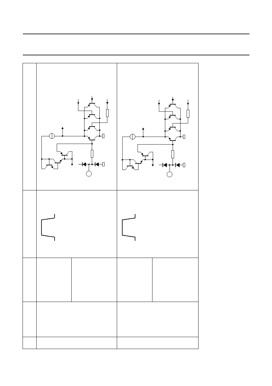
1997
Nov
25
34
Philips Semiconductors
Product specification
150 MHz video controller with I
2
C-bus
TDA4885
3
OSD
2
;
OSD input
channel 2
V
3
< V
P
-
1 V:
open-circuit base
V
3
= V
P
:
I
3
= 80 to 280
µ
A
4
OSD
3
;
OSD input
channel 3
V
4
< V
P
-
1 V:
open-circuit base
V
4
= V
P
:
I
4
= 80 to 280
µ
A
PIN
SYMBOL AND
DESCRIPTION
CHARACTERISTIC
WAVEFORM
EQUIVALENT CIRCUIT
MHA653
0 V
5 V
MHA930
50
µ
A
3
VP
VP
signal blanking
FBL
disable OSD
test
current
1 k
1 k
MHA653
0 V
5 V
MHA931
50
µ
A
4
VP
VP
signal blanking
FBL
disable OSD
test
current
1 k
1 k
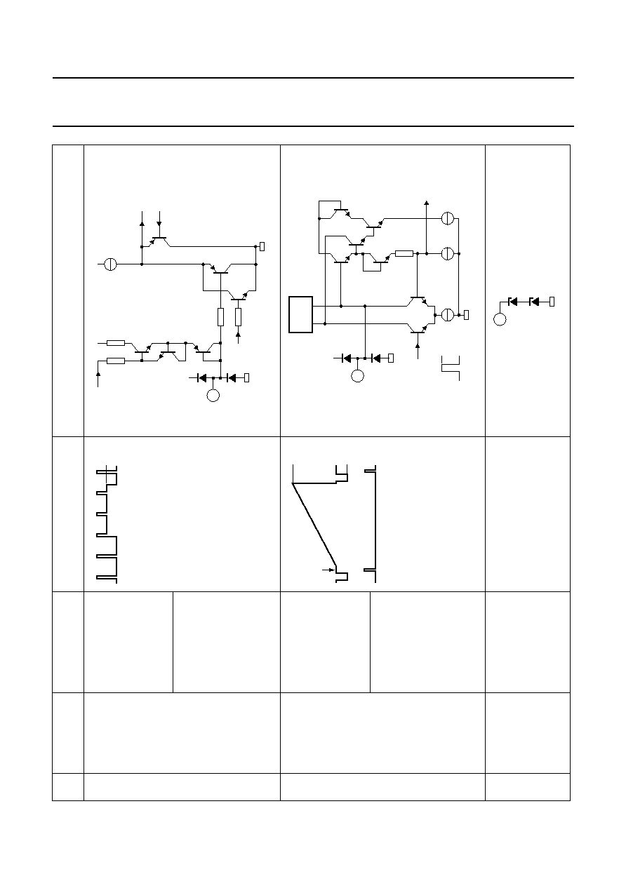
1997
Nov
25
35
Philips Semiconductors
Product specification
150 MHz video controller with I
2
C-bus
TDA4885
5
CLI;
vertical
blanking input
(input clamping)
V
5
> 0.2 V:
open-circuit base
V
5
0.2 V:
source current rising
with decreasing
voltage
6
V
I1
;
signal input
channel 1
outside clamping
pulse: open-circuit
base with base
current
compensation
during clamping:
I
6
=
-
150 to +150
µ
A
7
V
P
;
supply voltage
20 mA
PIN
SYMBOL AND
DESCRIPTION
CHARACTERISTIC
WAVEFORM
EQUIVALENT CIRCUIT
MHA651
5 V
0 V
2.5 V
MHA619
26
µ
A
5
VP
VP
power
on/down
1 k
10 k
10 k
6 k
2VBE
3 V
+
VBE
MHA652
sync
video signal
input clamping (pin 5)
black
shoulder
4.7 V
4 V
3.7 V
MHA620
240
µ
A
150
µ
A
0
µ
A
220
µ
A
signal
700
MIRROR
1 : 1
6
VP
VP
1.8 V
+
VBE
MHA621
7

1997
Nov
25
36
Philips Semiconductors
Product specification
150 MHz video controller with I
2
C-bus
TDA4885
8
V
I2
;
signal input
channel 2
outside clamping
pulse: open-circuit
base with base
current
compensation
during clamping:
I
6
=
-
150 to +150
µ
A
9
GND;
ground
10
V
I3
;
signal input
channel 3
outside clamping
pulse: open-circuit
base with base
current
compensation
during clamping:
I
6
=
-
150 to +150
µ
A
PIN
SYMBOL AND
DESCRIPTION
CHARACTERISTIC
WAVEFORM
EQUIVALENT CIRCUIT
MHA652
sync
video signal
input clamping (pin 5)
black
shoulder
4.7 V
4 V
3.7 V
MHA622
240
µ
A
150
µ
A
0
µ
A
220
µ
A
signal
700
MIRROR
1 : 1
8
VP
VP
1.8 V
+
VBE
MHA623
9
MHA652
sync
video signal
input clamping (pin 5)
black
shoulder
4.7 V
4 V
3.7 V
MHA624
240
µ
A
150
µ
A
0
µ
A
220
µ
A
signal
700
MIRROR
1 : 1
10
VP
VP
1.8 V
+
VBE

1997
Nov
25
37
Philips Semiconductors
Product specification
150 MHz video controller with I
2
C-bus
TDA4885
11
HFB;
horizontal
flyback input
(output
clamping,
blanking)
V
11
> 0.2 V:
open-circuit base
V
11
0.2 V:
source current rising
with decreasing
voltage
12
GM
1
;
gain modulation
input channel 1
R
12
= 20 k
;
open-circuit voltage
V
12
= 2.0 V
13
GM
2
;
gain modulation
input channel 2
R
13
= 20 k
;
open-circuit voltage
V
13
= 2.0 V
PIN
SYMBOL AND
DESCRIPTION
CHARACTERISTIC
WAVEFORM
EQUIVALENT CIRCUIT
MHA649
5 V
0 V
MHA625
27
µ
A
blanking
1.7 V
clamping
11
VP
VP
1 k
10 k
12 k
10 k
6 k
2VBE
3 V
+
VBE
power on/down
27
µ
A
MHA650
3 V
2 V
1 V
MHA626
12
VP
10 k
27.5 k
15.7 k
5.5 V
2.2 V
MHA650
3 V
2 V
1 V
MHA627
13
VP
10 k
27.5 k
15.7 k
5.5 V
2.2 V

1997
Nov
25
38
Philips Semiconductors
Product specification
150 MHz video controller with I
2
C-bus
TDA4885
14
GM
3
;
gain modulation
input channel 3
R
14
= 20 k
;
open-circuit voltage
V
14
= 2.0 V
15
SDA;
I
2
C-bus serial
data
input/output
no acknowledge;
open-circuit base
during
acknowledge:
I
15
= 4 mA
16
SCL;
I
2
C-bus clock
input
open-circuit base
PIN
SYMBOL AND
DESCRIPTION
CHARACTERISTIC
WAVEFORM
EQUIVALENT CIRCUIT
MHA650
3 V
2 V
1 V
MHA628
14
VP
10 k
27.5 k
15.7 k
5.5 V
2.2 V
MHA647
5 V
0 V
MHA629
15
acknowledge
10
k
3
µ
A
70
µ
A
19
µ
A
2.46 V
+
VBE
MHA648
5 V
0 V
MHA630
19
µ
A
10 k
2.46 V
+
VBE
16

1997
Nov
25
39
Philips Semiconductors
Product specification
150 MHz video controller with I
2
C-bus
TDA4885
17
LIM;
beam current
limiting input
open-circuit voltage
V
17
= 5.0 V
V
17
< 4.5 V:
open-circuit base
18
GND
3
;
ground
channel 3
19
V
P3
;
supply voltage
channel 3
I
19
= 40 mA
PIN
SYMBOL AND
DESCRIPTION
CHARACTERISTIC
WAVEFORM
EQUIVALENT CIRCUIT
MHA631
17
VP
5.0 V
1 k
21
µ
A
10 k
MHA632
18
MHA633
19
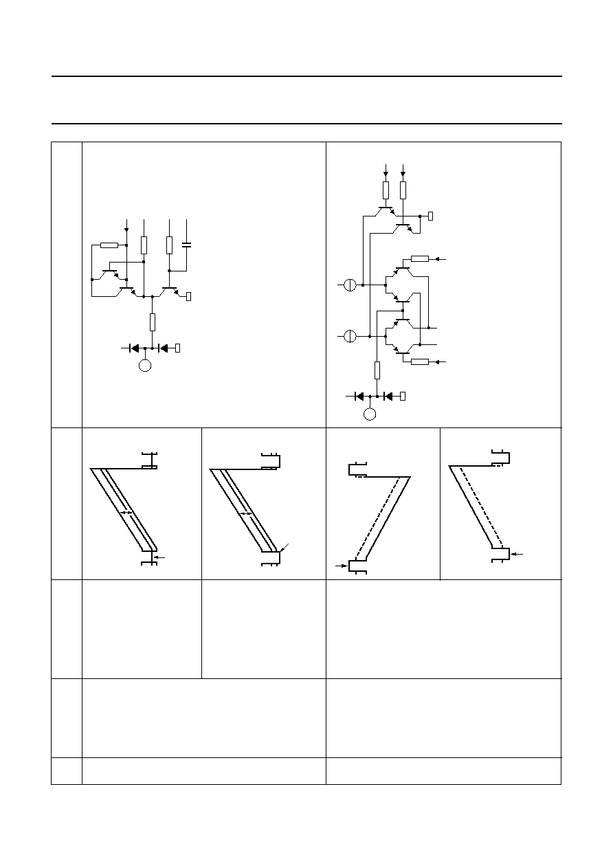
1997
Nov
25
40
Philips Semiconductors
Product specification
150 MHz video controller with I
2
C-bus
TDA4885
20
V
O3
;
signal output
channel 3
reference black level
0.1 to 2.8 V
control bit PEDST = 0
pedestal black level
0.1 to 2.8 V
control bit PEDST = 1
21
FB
3
;
feedback input
channel 3
open-circuit base
control bit FPOL = 0
control bit FPOL = 1
PIN
SYMBOL AND
DESCRIPTION
CHARACTERISTIC
WAVEFORM
EQUIVALENT CIRCUIT
MHA655
brightness
reference black level during output clamping
20
VP
VP
80
1.5 k
3.5 pF
8 k
500
MHA634
MHA656
brightness
pedestal black level during output clamping
MHA654
feedback reference 5.8 to 4 V
PEDST = 0
PEDST = 1
21
MHA635
VP
1 k
1 k
0.7 V
5.8 to 4 V
1 k
10
µ
A
10
µ
A
Vs1
Vs2
15 k
15 k
MHA660
feedback reference 0.7 V
PEDST = 0
PEDST = 1
DC coupling; Vs1 = 0 V; Vs2 = 1 V (control bit FPOL = 0)
AC coupling; Vs1 = 1 V; Vs2 = 0 V (control bit FPOL = 1)

1997
Nov
25
41
Philips Semiconductors
Product specification
150 MHz video controller with I
2
C-bus
TDA4885
22
REF
3
;
reference
voltage
channel 3
-
300 to +300
µ
A
23
GND
2
;
ground
channel 2
24
V
P2
;
supply voltage
channel 2
I
24
= 40 mA
PIN
SYMBOL AND
DESCRIPTION
CHARACTERISTIC
WAVEFORM
EQUIVALENT CIRCUIT
MHA636
5.8 to 4 V
300
µ
A
30
µ
A
15
µ
A
22
7.5
µ
A
VP
170
MHA637
23
MHA638
24

1997
Nov
25
42
Philips Semiconductors
Product specification
150 MHz video controller with I
2
C-bus
TDA4885
25
V
O2
;
signal output
channel 2
reference black level
0.1 to 2.8 V
control bit PEDST = 0
pedestal black level
0.1 to 2.8 V
control bit PEDST = 1
26
FB
2
;
feedback input
channel 2
open-circuit base
control bit FPOL = 0
control bit FPOL = 1
PIN
SYMBOL AND
DESCRIPTION
CHARACTERISTIC
WAVEFORM
EQUIVALENT CIRCUIT
MHA655
brightness
reference black level during output clamping
25
VP
VP
80
1.5 k
3.5 pF
8 k
500
MHA639
MHA656
brightness
pedestal black level during output clamping
MHA654
feedback reference 5.8 to 4 V
PEDST = 0
PEDST = 1
26
MHA640
VP
1 k
1 k
0.7 V
5.8 to 4 V
1 k
10
µ
A
10
µ
A
Vs1
Vs2
15 k
15 k
MHA660
feedback reference 0.7 V
PEDST = 0
PEDST = 1
DC coupling; Vs1 = 0 V; Vs2 = 1 V (control bit FPOL = 0)
AC coupling; Vs1 = 1 V; Vs2 = 0 V (control bit FPOL = 1)

1997
Nov
25
43
Philips Semiconductors
Product specification
150 MHz video controller with I
2
C-bus
TDA4885
27
REF
2
;
reference
voltage
channel 2
-
300 to +300
µ
A
28
GND
1
;
ground
channel 1
29
V
P1
;
supply voltage
channel 1
I
29
= 40 mA
PIN
SYMBOL AND
DESCRIPTION
CHARACTERISTIC
WAVEFORM
EQUIVALENT CIRCUIT
MHA641
5.8 to 4 V
300
µ
A
30
µ
A
15
µ
A
27
7.5
µ
A
VP
170
MHA642
28
MHA643
29

1997
Nov
25
44
Philips Semiconductors
Product specification
150 MHz video controller with I
2
C-bus
TDA4885
30
V
O1
;
signal output
channel 1
reference black level
0.1 to 2.8 V
control bit PEDST = 0
pedestal black level
0.1 to 2.8 V
control bit PEDST = 1
31
FB
1
;
feedback input
channel 1
open-circuit base
control bit FPOL = 0
control bit FPOL = 1
PIN
SYMBOL AND
DESCRIPTION
CHARACTERISTIC
WAVEFORM
EQUIVALENT CIRCUIT
MHA655
brightness
reference black level during output clamping
30
VP
VP
80
1.5 k
3.5 pF
8 k
500
MHA644
MHA656
brightness
pedestal black level during output clamping
MHA654
feedback reference 5.8 to 4 V
PEDST = 0
PEDST = 1
31
MHA645
VP
1 k
1 k
0.7 V
5.8 to 4 V
1 k
10
µ
A
10
µ
A
Vs1
Vs2
15 k
15 k
MHA660
feedback reference 0.7 V
PEDST = 0
PEDST = 1
DC coupling; Vs1 = 0 V; Vs2 = 1 V (control bit FPOL = 0)
AC coupling; Vs1 = 1 V; Vs2 = 0 V (control bit FPOL = 1)
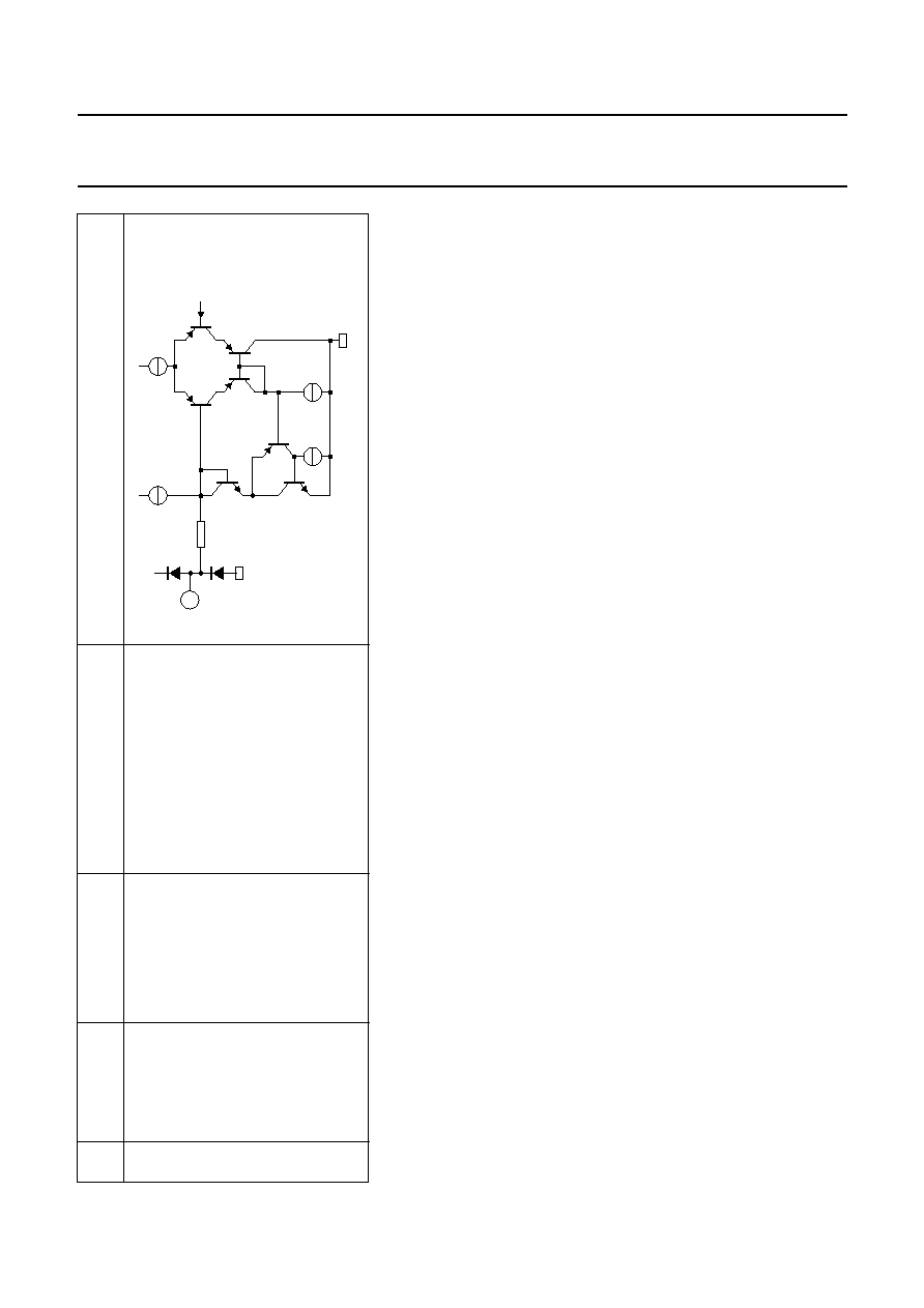
1997
Nov
25
45
Philips Semiconductors
Product specification
150 MHz video controller with I
2
C-bus
TDA4885
32
REF
1
;
reference
voltage
channel 1
-
300 to +300
µ
A
PIN
SYMBOL AND
DESCRIPTION
CHARACTERISTIC
WAVEFORM
EQUIVALENT CIRCUIT
MHA646
5.8 to 4 V
300
µ
A
30
µ
A
15
µ
A
32
7.5
µ
A
VP
170

1997 Nov 25
46
Philips Semiconductors
Product specification
150 MHz video controller with I
2
C-bus
TDA4885
13 TEST AND APPLICATION INFORMATION
Fig.18 Basic application for different output stages with DC coupling (FPOL = 0) or AC coupling (FPOL = 1).
handbook, full pagewidth
MHA927
BLACK LEVEL
RESTORATION
to cathode
to cathode
to cathode
32
31
30
29
28
27
26
25
24
23
22
21
20
19
18
17
16
GND
beam current limiting;
subcontrast setting
15
14
13
12
11
10
9
8
7
6
5
4
3
2
1
I
2
C-BUS
input clamping
vertical blanking
output clamping
blanking
signal
inputs
OSD inputs
fast blanking
VCRT = 90 V
VCRT = 70 V
VCRT = 90 V
n.c.
n.c.
VP = 8 V
TDA4885

1997 Nov 25
47
Philips Semiconductors
Product specification
150 MHz video controller with I
2
C-bus
TDA4885
13.1
Test application
For high frequency measurements a special test
application and printed-circuit board with only a few
external components is built. Figure 19 shows the test
application circuit and Figs 20 and 21 the layout of the
double sided printed board. Most components are of SMD
type. Short HF loops and minimum crosstalk between the
channels and between signal inputs and outputs are
achieved by properly shaped ground areas.
The HF input signal can be fed to the subclick connectors
V
I1
, V
I2
and V
I3
by a 50
line. The line is then terminated
by a 50
resistor on the board. In channel 3 (pin 10) the
HF input signal can be measured (probe socket).
For operation without input clamping the DC bias can be
provided by VINDC if a short-circuit at J1, J2 and J3 is
made.
OSD input signals (subclick: OSD
1
, OSD
2
, OSD
3
, FBL)
and blanking/clamping inputs (subclick: CLI, HFB) are
terminated with 50
on the board.
The gain modulation input GM (subclick) can be
connected to the three inputs by the jumpers J8 and J4, J5
and J6. With jumper J7 pins 12, 13 and 14 can be
connected to ground (no gain reduction).
There is a separate 4-pin connector for the I
2
C-bus
controller, SDA and SCL have 10 k
pull up resistors to
5 V digital supply.
The beam current limiting pin is fed to the 10-pin main
connector without any special application and should be
connected to the 5 V supply if not used.
DC supply voltage V
P
with a series resistor of 5.6
can be
measured directly at pin 7 via a resistor of 1 k
(V
P
sense).
The supply voltage for the signal channels is fed to VPX
separately and connected to pins 19, 24 and 29 with
decoupling resistors of 5.6
. The supply voltage V
P1
(pin 29) can be measured via 1 k
at pin V
P1
sense.
All supply voltages are filtered near to their pins with
150 pF and 100 nF SMD capacitors and low impedance
0.47
µ
F/63 V electrolytic capacitors.
The signal outputs are loaded with 10 k
and 3 pF to
ground and are connected to a probe socket. With a probe
capacitance of 2 pF the total capacitive load is 5 pF.
The feedback inputs are connected to the voltage outputs
with a 0
resistor (short circuit; RFB1) and via 10 k
(RFB2) connected to the pin VFBDC. The blanking level
can be adjusted with a variation of RFB1, RFB2 and
VFBDC but the resistive output load will be changed.
The blanking level is:
The reference outputs are connected to solder pins.
U
outbl
1
RFB1
RFB2
----------------
+
0.7 V
◊
RFB1
RFB2
----------------
VFBDC
◊
≠
=

1997 Nov 25
48
Philips Semiconductors
Product specification
150 MHz video controller with I
2
C-bus
TDA4885
Fig.19 Test board.
handbook, full pagewidth
MHA657
50
50
5 k
0.47
µ
F
(63 V)
0.47
µ
F
(63 V)
100
pF
150 pF
10 nF
100
nF
150
pF
100
nF
CLI
VP
VI2
VI1
CLI
50
5.6
1 k
FBL
FBL
VI1
VI2
VI3
VI3
GM1
GM2
GM3
SDA
SCL
HFB
GND
VP2
VO2
3 pF
FB2
REF2
GND2
GND1
50
OSD3
OSD3
50
OSD2
OSD2
50
OSD1
OSD1
10 k
10 k
RFB2
10 k
RFB1
5.6
5.6
1 k
J2
5 k
10 k
10 k
J3
J4
J5
J6
J8
J7
probe
5 k
J1
50
150 pF
10 nF
50
HFB
GM
SDA
5 V
SCL
50
150 pF
10 nF
1
2
3
4
5
6
solder pin
7
8
9
10
11
12
13
14
15
16
32
31
30
29
28
27
26
25
24
23
22
21
20
19
18
17
REF3
GND3
LIM
FB3
VO3
VP3
VP1
VO1
FB1
REF1
TDA4885
channel 3
channel 2
channel 1
VPX
VO3
VO2
VO1
VP1 sense
VFBDC
VP sense
VP
GND
VINDC
LIM
5 V

1997 Nov 25
49
Philips Semiconductors
Product specification
150 MHz video controller with I
2
C-bus
TDA4885
Fig.20 Component layout and printed-circuit board; side A (for side B see Fig.21).
handbook, full pagewidth
MHA658
76.20
116.84
OSD3 OSD2 OSD1
FBL
100 nF
150 pF
J1
CLI
VI1
VI2
VI3
VO3
VP
SCL
SDA
GND
J2
J3
JP
J7 J8
J6
J4
J5
GM
HFB
TP
TP
VO2
TP
VO1
5.6
1 k
10 k
10 k
MP
MP
MP
10 k
10 k
10 k
10 k
10 k
3.3 pF
3.3 pF
3.3 pF
10 k
0.47
µ
F
0.47
µ
F
0.47
µ
F
0.47
µ
F
10 k
TP
I
2
C-bus
IC1

1997 Nov 25
50
Philips Semiconductors
Product specification
150 MHz video controller with I
2
C-bus
TDA4885
Fig.21 Component layout and printed-circuit board; side B (for side A see Fig.20).
handbook, full pagewidth
MHA659
76.20
116.84
50
1 k
5.6
5.6
5.6
100 nF
100 nF
150 pF
150 pF
100 nF
150 pF
100 nF
150 pF
50
50
50
50
50
5 k
10 nF
150 pF
5 k
10 nF
150 pF
5 k
10 nF
150 pF
50
50
50
10 k
10 k

1997 Nov 25
51
Philips Semiconductors
Product specification
150 MHz video controller with I
2
C-bus
TDA4885
13.2
Recommendations for building the application
board
∑
General
≠ Double-sided board
≠ Short HF loops by large ground plane on the rear
≠ SMD components with minimum parasitics.
∑
Voltage outputs
≠ Capacitive loads as small as possible
≠ Be aware of internal output resistance (80
).
∑
Supply voltages
≠ Capacitors as near as possible to the pins
≠ Use electrolytic capacitors with small serial
resistance and inductance.
∑
Smearing
≠ Additional peaking circuit at emitter of driver
transistor of cascode stage (time constant
approximately 100 ns).

1997 Nov 25
52
Philips Semiconductors
Product specification
150 MHz video controller with I
2
C-bus
TDA4885
14 PACKAGE OUTLINE
UNIT
b
1
c
E
e
M
H
L
REFERENCES
OUTLINE
VERSION
EUROPEAN
PROJECTION
ISSUE DATE
IEC
JEDEC
EIAJ
mm
DIMENSIONS (mm are the original dimensions)
SOT232-1
92-11-17
95-02-04
b
max.
w
M
E
e
1
1.3
0.8
0.53
0.40
0.32
0.23
29.4
28.5
9.1
8.7
3.2
2.8
0.18
1.778
10.16
10.7
10.2
12.2
10.5
1.6
4.7
0.51
3.8
M
H
c
(e )
1
M
E
A
L
seating plane
A
1
w
M
b
1
e
D
A
2
Z
32
1
17
16
b
E
pin 1 index
0
5
10 mm
scale
Note
1. Plastic or metal protrusions of 0.25 mm maximum per side are not included.
(1)
(1)
D
(1)
Z
A
max.
1
2
A
min.
A
max.
SDIP32: plastic shrink dual in-line package; 32 leads (400 mil)
SOT232-1

1997 Nov 25
53
Philips Semiconductors
Product specification
150 MHz video controller with I
2
C-bus
TDA4885
15 SOLDERING
15.1
Introduction
There is no soldering method that is ideal for all IC
packages. Wave soldering is often preferred when
through-hole and surface mounted components are mixed
on one printed-circuit board. However, wave soldering is
not always suitable for surface mounted ICs, or for
printed-circuits with high population densities. In these
situations reflow soldering is often used.
This text gives a very brief insight to a complex technology.
A more in-depth account of soldering ICs can be found in
our
"IC Package Databook" (order code 9398 652 90011).
15.2
Soldering by dipping or by wave
The maximum permissible temperature of the solder is
260
∞
C; solder at this temperature must not be in contact
with the joint for more than 5 seconds. The total contact
time of successive solder waves must not exceed
5 seconds.
The device may be mounted up to the seating plane, but
the temperature of the plastic body must not exceed the
specified maximum storage temperature (T
stg max
). If the
printed-circuit board has been pre-heated, forced cooling
may be necessary immediately after soldering to keep the
temperature within the permissible limit.
15.3
Repairing soldered joints
Apply a low voltage soldering iron (less than 24 V) to the
lead(s) of the package, below the seating plane or not
more than 2 mm above it. If the temperature of the
soldering iron bit is less than 300
∞
C it may remain in
contact for up to 10 seconds. If the bit temperature is
between 300 and 400
∞
C, contact may be up to 5 seconds.
16 DEFINITIONS
17 LIFE SUPPORT APPLICATIONS
These products are not designed for use in life support appliances, devices, or systems where malfunction of these
products can reasonably be expected to result in personal injury. Philips customers using or selling these products for
use in such applications do so at their own risk and agree to fully indemnify Philips for any damages resulting from such
improper use or sale
18 PURCHASE OF PHILIPS I
2
C COMPONENTS
Data sheet status
Objective specification
This data sheet contains target or goal specifications for product development.
Preliminary specification
This data sheet contains preliminary data; supplementary data may be published later.
Product specification
This data sheet contains final product specifications.
Limiting values
Limiting values given are in accordance with the Absolute Maximum Rating System (IEC 134). Stress above one or
more of the limiting values may cause permanent damage to the device. These are stress ratings only and operation
of the device at these or at any other conditions above those given in the Characteristics sections of the specification
is not implied. Exposure to limiting values for extended periods may affect device reliability.
Application information
Where application information is given, it is advisory and does not form part of the specification.
Purchase of Philips I
2
C components conveys a license under the Philips' I
2
C patent to use the
components in the I
2
C system provided the system conforms to the I
2
C specification defined by
Philips. This specification can be ordered using the code 9398 393 40011.

1997 Nov 25
54
Philips Semiconductors
Product specification
150 MHz video controller with I
2
C-bus
TDA4885
NOTES

1997 Nov 25
55
Philips Semiconductors
Product specification
150 MHz video controller with I
2
C-bus
TDA4885
NOTES

Internet: http://www.semiconductors.philips.com
Philips Semiconductors ≠ a worldwide company
© Philips Electronics N.V. 1997
SCA56
All rights are reserved. Reproduction in whole or in part is prohibited without the prior written consent of the copyright owner.
The information presented in this document does not form part of any quotation or contract, is believed to be accurate and reliable and may be changed
without notice. No liability will be accepted by the publisher for any consequence of its use. Publication thereof does not convey nor imply any license
under patent- or other industrial or intellectual property rights.
Netherlands: Postbus 90050, 5600 PB EINDHOVEN, Bldg. VB,
Tel. +31 40 27 82785, Fax. +31 40 27 88399
New Zealand: 2 Wagener Place, C.P.O. Box 1041, AUCKLAND,
Tel. +64 9 849 4160, Fax. +64 9 849 7811
Norway: Box 1, Manglerud 0612, OSLO,
Tel. +47 22 74 8000, Fax. +47 22 74 8341
Philippines: Philips Semiconductors Philippines Inc.,
106 Valero St. Salcedo Village, P.O. Box 2108 MCC, MAKATI,
Metro MANILA, Tel. +63 2 816 6380, Fax. +63 2 817 3474
Poland: Ul. Lukiska 10, PL 04-123 WARSZAWA,
Tel. +48 22 612 2831, Fax. +48 22 612 2327
Portugal: see Spain
Romania: see Italy
Russia: Philips Russia, Ul. Usatcheva 35A, 119048 MOSCOW,
Tel. +7 095 755 6918, Fax. +7 095 755 6919
Singapore: Lorong 1, Toa Payoh, SINGAPORE 1231,
Tel. +65 350 2538, Fax. +65 251 6500
Slovakia: see Austria
Slovenia: see Italy
South Africa: S.A. PHILIPS Pty Ltd., 195-215 Main Road Martindale,
2092 JOHANNESBURG, P.O. Box 7430 Johannesburg 2000,
Tel. +27 11 470 5911, Fax. +27 11 470 5494
South America: Al. Vicente Pinzon, 173, 6th floor,
04547-130 S√O PAULO, SP, Brazil,
Tel. +55 11 821 2333, Fax. +55 11 821 2382
Spain: Balmes 22, 08007 BARCELONA,
Tel. +34 3 301 6312, Fax. +34 3 301 4107
Sweden: Kottbygatan 7, Akalla, S-16485 STOCKHOLM,
Tel. +46 8 632 2000, Fax. +46 8 632 2745
Switzerland: Allmendstrasse 140, CH-8027 ZÐRICH,
Tel. +41 1 488 2686, Fax. +41 1 481 7730
Taiwan: Philips Semiconductors, 6F, No. 96, Chien Kuo N. Rd., Sec. 1,
TAIPEI, Taiwan Tel. +886 2 2134 2865, Fax. +886 2 2134 2874
Thailand: PHILIPS ELECTRONICS (THAILAND) Ltd.,
209/2 Sanpavuth-Bangna Road Prakanong, BANGKOK 10260,
Tel. +66 2 745 4090, Fax. +66 2 398 0793
Turkey: Talatpasa Cad. No. 5, 80640 GÐLTEPE/ISTANBUL,
Tel. +90 212 279 2770, Fax. +90 212 282 6707
Ukraine: PHILIPS UKRAINE, 4 Patrice Lumumba str., Building B, Floor 7,
252042 KIEV, Tel. +380 44 264 2776, Fax. +380 44 268 0461
United Kingdom: Philips Semiconductors Ltd., 276 Bath Road, Hayes,
MIDDLESEX UB3 5BX, Tel. +44 181 730 5000, Fax. +44 181 754 8421
United States: 811 East Arques Avenue, SUNNYVALE, CA 94088-3409,
Tel. +1 800 234 7381
Uruguay: see South America
Vietnam: see Singapore
Yugoslavia: PHILIPS, Trg N. Pasica 5/v, 11000 BEOGRAD,
Tel. +381 11 625 344, Fax.+381 11 635 777
For all other countries apply to: Philips Semiconductors,
International Marketing & Sales Communications, Building BE-p,
P.O. Box 218, 5600 MD EINDHOVEN, The Netherlands, Fax. +31 40 27 24825
Argentina: see South America
Australia: 34 Waterloo Road, NORTH RYDE, NSW 2113,
Tel. +61 2 9805 4455, Fax. +61 2 9805 4466
Austria: Computerstr. 6, A-1101 WIEN, P.O. Box 213, Tel. +43 160 1010,
Fax. +43 160 101 1210
Belarus: Hotel Minsk Business Center, Bld. 3, r. 1211, Volodarski Str. 6,
220050 MINSK, Tel. +375 172 200 733, Fax. +375 172 200 773
Belgium: see The Netherlands
Brazil: see South America
Bulgaria: Philips Bulgaria Ltd., Energoproject, 15th floor,
51 James Bourchier Blvd., 1407 SOFIA,
Tel. +359 2 689 211, Fax. +359 2 689 102
Canada: PHILIPS SEMICONDUCTORS/COMPONENTS,
Tel. +1 800 234 7381
China/Hong Kong: 501 Hong Kong Industrial Technology Centre,
72 Tat Chee Avenue, Kowloon Tong, HONG KONG,
Tel. +852 2319 7888, Fax. +852 2319 7700
Colombia: see South America
Czech Republic: see Austria
Denmark: Prags Boulevard 80, PB 1919, DK-2300 COPENHAGEN S,
Tel. +45 32 88 2636, Fax. +45 31 57 0044
Finland: Sinikalliontie 3, FIN-02630 ESPOO,
Tel. +358 9 615800, Fax. +358 9 61580920
France: 51 Rue Carnot, BP317, 92156 SURESNES Cedex,
Tel. +33 1 40 99 6161, Fax. +33 1 40 99 6427
Germany: Hammerbrookstraþe 69, D-20097 HAMBURG,
Tel. +49 40 23 53 60, Fax. +49 40 23 536 300
Greece: No. 15, 25th March Street, GR 17778 TAVROS/ATHENS,
Tel. +30 1 4894 339/239, Fax. +30 1 4814 240
Hungary: see Austria
India: Philips INDIA Ltd, Band Box Building, 2nd floor,
254-D, Dr. Annie Besant Road, Worli, MUMBAI 400 025,
Tel. +91 22 493 8541, Fax. +91 22 493 0966
Indonesia: see Singapore
Ireland: Newstead, Clonskeagh, DUBLIN 14,
Tel. +353 1 7640 000, Fax. +353 1 7640 200
Israel: RAPAC Electronics, 7 Kehilat Saloniki St, PO Box 18053,
TEL AVIV 61180, Tel. +972 3 645 0444, Fax. +972 3 649 1007
Italy: PHILIPS SEMICONDUCTORS, Piazza IV Novembre 3,
20124 MILANO, Tel. +39 2 6752 2531, Fax. +39 2 6752 2557
Japan: Philips Bldg 13-37, Kohnan 2-chome, Minato-ku, TOKYO 108,
Tel. +81 3 3740 5130, Fax. +81 3 3740 5077
Korea: Philips House, 260-199 Itaewon-dong, Yongsan-ku, SEOUL,
Tel. +82 2 709 1412, Fax. +82 2 709 1415
Malaysia: No. 76 Jalan Universiti, 46200 PETALING JAYA, SELANGOR,
Tel. +60 3 750 5214, Fax. +60 3 757 4880
Mexico: 5900 Gateway East, Suite 200, EL PASO, TEXAS 79905,
Tel. +9-5 800 234 7381
Middle East: see Italy
Printed in The Netherlands
547047/1200/02/pp56
Date of release: 1997 Nov 25
Document order number:
9397 750 02705