 | –≠–ª–µ–∫—Ç—Ä–æ–Ω–Ω—ã–π –∫–æ–º–ø–æ–Ω–µ–Ω—Ç: TDA5030A | –°–∫–∞—á–∞—Ç—å:  PDF PDF  ZIP ZIP |
Document Outline
- DESCRIPTION
- APPLICATIONS
- PIN CONFIGURATION
- FEATURES
- ORDERING INFORMATION
- ABSOLUTE MAXIMUM RATINGS
- PIN DESCRIPTIONS
- DC ELECTRICAL CHARACTERISTICS
- AC ELECTRICAL CHARACTERISTICS
- APPLICATIONS INFORMATION
- TIMING DIAGRAM
- BLOCK DIAGRAM AND TEST CIRCUIT
Philips Semiconductors
Product specification
NE5241
Dolby ADM digital audio decoder
1
March 19, 1992
853-1602 06126
DESCRIPTION
The NE5241 is a complete stereo digital to audio converter for the
Dolby ADM digital audio system, which allows CD quality stereo
audio to be delivered with data rates on the order of 400 to 600kb/s.
The NE5241 is intended for use in high quality consumer digital
audio equipment for the reproduction of broadcast (or pre-recorded)
digital audio. The IC contains channel de-multiplexing data input
latches, control signal filter drivers and buffers, variable gain
integrators, and variable de-emphasis filters. Precision, temperature
compensated voltage reference circuitry assures accurate
performance over temperature. The IC is implemented in a bipolar
process to achieve low noise, low distortion, and wide dynamic
range. The NE5241 is an improved version of the NE5240, which
has been discontinued.
Note:
The NE5241 is available only to licensees of Dolby Laboratories Licensing Corporation,
from who licensing and applications information must be obtained. Dolby is a registered
trademark of Dolby Laboratories Licensing Corporation, San Francisco, California.
APPLICATIONS
∑
High quality digital audio transmission systems
∑
Pre-recorded digital audio
∑
Satellite delivered digital audio
∑
Cable TV delivered digital audio
∑
Microwave delivered digital audio
∑
Terrestrial delivered digital audio
∑
Digital audio for advanced television sound
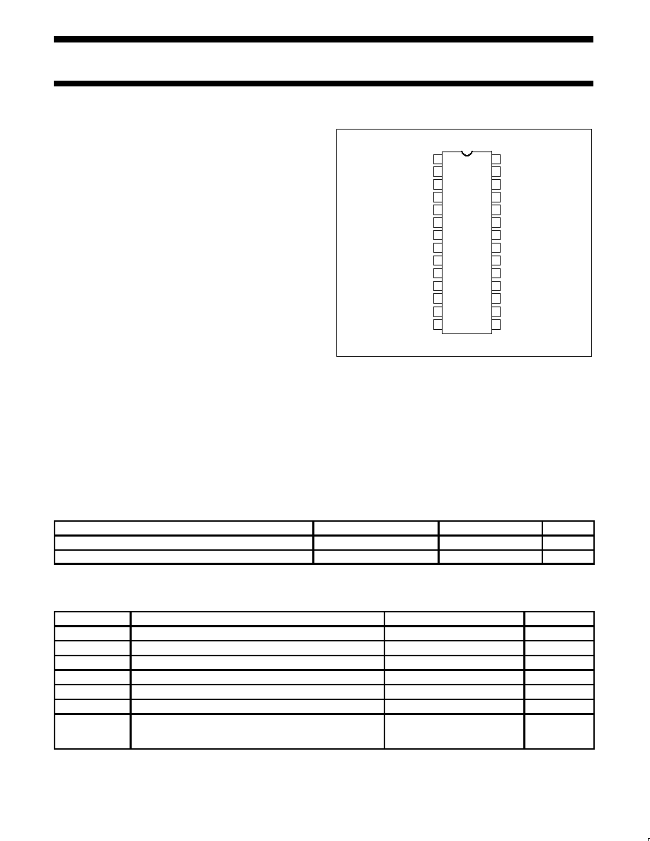
PIN CONFIGURATION
N, D Packages
MULTI OUT 1
VCC
VARZ 1
OUT 1
TOP VIEW
1
2
3
4
5
6
7
8
9
10
11
12
13
14
24
23
22
21
20
19
18
17
16
15
25
26
27
28
FEEDBACK 1
INT IN 1
EM FILT IN 1
EM FILT OUT 1
SS FILT IN 1
SS FILT OUT 1
VDD
SS
AD
EM
MULTI OUT 2
AGND
VARZ 2
OUT 2
FEEDBACK 2
INT IN 2
EM FILT IN 2
EM FILT OUT 2
SS FILT IN 2
SS FILT OUT 2
DGND
REX
VREF
CK
SR01021
Figure 1. Pin Configuration
FEATURES
∑
Wide dynamic range: >95dB
∑
Low distortion: <0.1% @ 1kHz, 0dB
∑
TTL, CMOS compatible logic inputs
∑
Wide bandwidth: DC to > 20kHz
∑
Complete decoder implementation in one IChip
ORDERING INFORMATION
DESCRIPTION
TEMPERATURE RANGE
ORDER CODE
DWG #
28-Pin Plastic Dual In-Line Package (DIP)
0 to +70
∞
C
NE5241N
SOT117-2
28-Pin Small Outline Large (SOL) Package
0 to +70
∞
C
NE5241D
SOT136-1
ABSOLUTE MAXIMUM RATINGS
SYMBOL
PARAMETER
RATING
UNIT
V
CC
Analog supply voltage
+15
V
V
DD
Logic supply voltage
+7
V
T
A
Operating ambient temperature range
0 to +70
∞
C
T
STG
Storage temperature range
≠65 to +150
∞
C
T
J
Junction temperature
≠65 to +150
∞
C
T
SOLD
Lead temperature (soldering 60 sec)
+300
∞
C
JA
Thermal impedance
N package
D package
48
70
∞
C/W
∞
C/W

Philips Semiconductors
Product specification
NE5241
Dolby ADM digital audio decoder
March 19, 1992
2
PIN DESCRIPTIONS
PIN #
SYMBOL
DESCRIPTION
1
MULTI OUT 1
Multiplier output, channel 1
2
V
CC
Analog supply voltage
3
VARZ 1
Variable impedance, channel 1
4
OUT 1
Main output, channel 1
5
FEEDBACK 1
Summing amp input, channel 1
6
INT IN 1
Integrator amp input, channel 1
7
EM FILTER IN 1
Emphasis filter buffer input, channel 1
8
EM FILTER OUT 1
Emphasis filter driver output, channel 1
9
SS FILTER IN 1
Step-size filter buffer input, channel 1
10
SS FILTER OUT 1
Step-size filter driver output, channel 1
11
V
DD
Logic supply voltage
12
SS
Step-size data input
13
AD
Audio data input
14
EM
Emphasis data input
15
CK
Data clock input
16
V
REF
Reference voltage bypass
17
REX
Variable impedance reference resistor
18
D
GND
Digital ground
19
SS FILTER OUT 2
Step-size filter driver output, channel 2
20
SS FILTER IN 2
Step-size filter buffer input, channel 2
21
EM FILTER OUT 2
Emphasis filter driver output, channel 2
22
EM FILTER IN 2
Emphasis filter buffer input, channel 2
23
INT IN 2
Integrator amp input, channel 2
24
FEEDBACK 2
Summing amp input, channel 2
25
OUT 2
Main output, channel 2
26
VARZ 2
Variable impedance, channel 2
27
A
GND
Analog ground
28
MULT OUT 2
Multiplier output, channel 2

Philips Semiconductors
Product specification
NE5241
Dolby ADM digital audio decoder
March 19, 1992
3
DC ELECTRICAL CHARACTERISTICS
All specifications are at T
A
=25
∞
C, V
DD
=5V, V
CC
=12V. Test circuit Figure 1.
SYMBOL
PARAMETER
TEST CONDITIONS
LIMITS
UNIT
SYMBOL
PARAMETER
TEST CONDITIONS
Min
Typ
Max
UNIT
V
CC
Analog supply voltage
10.8
12
13.2
V
V
DD
Digital supply voltage
4.7
5
5.3
V
I
CC
Analog supply current
25
40
mA
I
DD
Digital supply current
12
20
mA
V
IH
HIGH level input voltage
2.0
V
V
IL
LOW level input voltage
Pins SS, AD, EM
0.8
V
I
IH
HIGH level input current
Pins SS, AD, EM = 2V
1
10
µ
A
I
IL
LOW level input current
Pins SS, AD, EM = 0.8V
1
5
µ
A
t
S
Data setup time
150
ns
t
H
Data hold time
150
ns
I
B
Control signal buffer bias current
10
30
nA
Integrating amp gain
22
dB
AC ELECTRICAL CHARACTERISTICS
All specifications are at T
A
=25
∞
C, V
DD
=5V, V
CC
=12V, Audio data rate = 204kHz. 0dB is defined as 0.775V
RMS
. Test circuit Figure 4.
SYMBOL
PARAMETER
TEST CONDITIONS
LIMITS
UNIT
SYMBOL
PARAMETER
TEST CONDITIONS
Min
Typ
Max
UNIT
Output voltage (reference level)
1
≠6
≠4.5
≠2.5
dBu
Channel balance (reference level)
1
0.2
1.2
dB
Channel balance change
2
20% < SS < 80%
0.2
1.0
dB
Channel balance change
2
10% < SS < 90%
0.4
1.5
dB
Step-size tracking error
3
20% < SS < 80%
0.5
3.0
dB
Step-size tracking error
3
10% < SS < 90%
1.0
4.0
dB
Headroom
4
13
Noise
5
20Hz ≠ 20kHz
≠80
≠78
dBu
Noise
5
CCIR/ARM
≠89
≠85
dBu
Mute noise
6
CCIR/ARM
≠93
≠88
dBu
Dynamic range
7
98
THD
Total harmonic distortion
1
0dB (ref level)
0.8
0.2
%
THD
Total harmonic distortion
8
+13dB (max level)
0.13
0.5
%
Variable de-emph calibration error
9
8kHz E
M
= 40%
≠1
0.2
1
dB
Freq. response error
2kHz E
M
= 10%
≠1.8
0.2
1.5
dB
Freq. response error
12kHz E
M
= 60%
≠2.3
0.25
2.3
dB
Freq. response error
15kHz E
M
= 70%
≠2.5
0.5
2.5
dB
Dynamic offset, emphasis
10
AC measurement
≠43
≠30
dB
Dynamic offset, step-size
11
AC measurement
≠39
≠24
dB
Channel separation
1kHz
75
dB
NOTES: Test patterns referred to are produced by the Dolby Cat. No. 346 ADM Test Data Generator.
1. Dolby ADM reference level, Dolby test pattern 00. This is 10dB below the nominal 100% modulation level.
2. The channel balance may change over the operating range. This specification is the channel balance change from the intial channel
balance which was measured at reference level.
3. The gain should change by 36.12dB as the step-size data is changed from 20% to 80% duty cycle, or 48.16dB as the data changes from
10% to 90%. The tracking error is the amount by which the gain change deviates from the desired value.
4. This is headroom over Dolby ADM reference level.
5. Idling data patterns, Dolby test pattern 02 with respect to test 01.
6. Muted data patterns, Dolby test pattern 04.
7. Difference between output voltage plus headroom, and CCIR/ARM weighted mute noise level.
8. Test level is 13dB over Dolby ADM reference level. Dolby test pattern 08.
9. Measured at 8.00kHz, with emphasis data at 40% duty cycle. This may be trimmed to zero by adjusting the resistor at Pin 17.
10. Dolby test pattern 48 relative to test 00. Duty cycle alternates from 10 to 70%.
11. Dolby test pattern 49 relative to test 00. Duty cycle alternates from 10 to 70%.
Philips Semiconductors
Product specification
NE5241
Dolby ADM digital audio decoder
March 19, 1992
4
APPLICATIONS INFORMATION
The application diagram shows the complete Dolby ADM decoder
using the NE5241. The decoder is followed by a line driving
amplifier, which, depending on the application, may not be
necessary. For best frequency response accuracy, the following
parts should be tight tolerance: R13 to R21 should be 1%, and C13
to C20 should be 2.5%. The variable de-emphasis pole position
may be trimmed by adjusting the value of R17. The variable
impedance Pins 3 and 26 are very sensitive to noise pickup. Keep
the lead to C15 and C18 as short as possible. Excessive stray
capacitance on the multiplier output, Pins 1 and 28, will adversely
affect performance. Keep the leads to R13 and R19 short. It is
desirable to place a ground plane under the NE5241. This reduces
the inevitable cross-talk of the digital data (with several volts of
swing) into the audio (which has a noise level on the order of 40
µ
V).
A ground plane is necessary to obtain the ultimate in noise
performance.
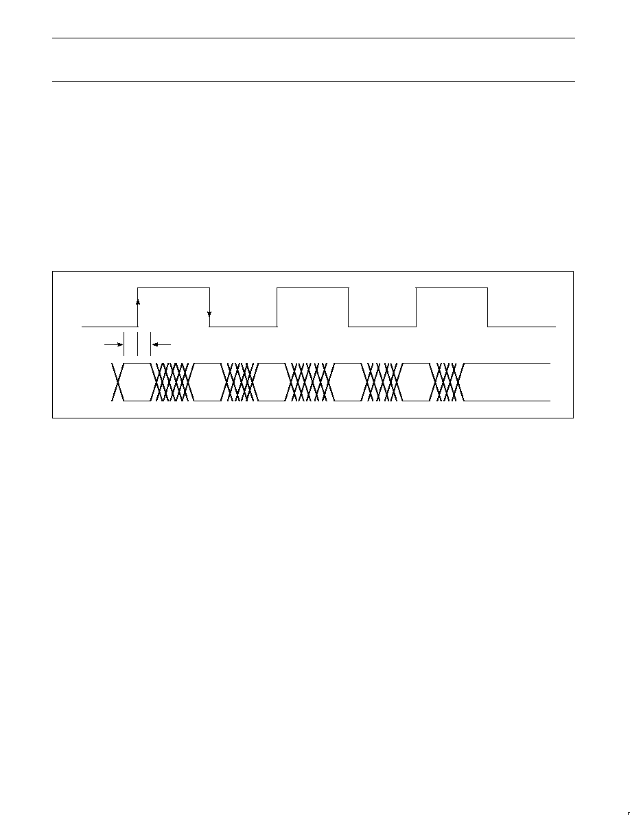
The timing diagram illustrates how the data is clocked into the
NE5241. The two audio channels share the three data input lines:
audio data, step-size data, and emphasis data. During the
low-to-high clock transition, the data is clocked into channel 1.
During the high-to-low clock transition, the data is clocked into
channel 2. The data must be stable during the clock transition.
TIMING DIAGRAM
tS tH
AUDIO DATA
STEP-SIZE DATA
EMPHASIS DATA
CH 1
CH 2
CH 1
CH 2
CH 1
CLOCK
SR01022
Figure 2. Timing Diagram

Philips Semiconductors
Product specification
NE5241
Dolby ADM digital audio decoder
March 19, 1992
5
BLOCK DIAGRAM AND TEST CIRCUIT
NE5241
R1
4.3k
12
13
14
15
18
19 21
22 20
28
23
24
25
26
27
16
17
2
3
4
5
6
1
9
7
8
10
11
INPUT
LOGIC
INTEGRATOR
AMP
SUMMING
AMP
REFERENCE
GENERATOR
INTEGRATOR
AMP
SUMMING
AMP
R2
43k
R3
360k
R4
4.3k
R5
43k
R6
360k
C3
4.7nF
C2
47nF
C1
0.47
µ
F
C4
0.47
µ
F
C6
4.7nF
C5
47nF
R13
4.99k
C13
0.1
µ
F
R15
4.87k
R14
499k
C14
10nF
22dB
14dB
C15
220pF
R16
6.34k
C16
3.9nF
R17
118k
C17
220
µ
F
C18
220pF
R18
6.34k
C19
3.9nF
≠
+
≠
+
SSD
AD
SBD
CK
CH.A
CH.B
VDD
VDD
DGND
eX
eX
VOUT
VOUT
VH
VR
VL
REX
AGND
VREF
NOTE:
One channel of the application shown with external components.
VCC
SR01023
Figure 3. Block Diagram and Test Circuit

Philips Semiconductors
Product specification
NE5241
Dolby ADM digital audio decoder
March 19, 1992
6
NE5241
R1
4.3k
9
7
8
10
R2
43k
R3
360k
R4
4.3k
R5
43k
R6
360k
C3
4.7nF
C2
47nF
C1
0.47
µ
F
C4
0.47
µ
F
C6
4.7nF
C5
47nF
R7
4.3k
20
22
21
19
R8
43k
R9
360k
R10
4.3k
R11
43k
R12
360k
C9
4.7nF
C8
47nF
C7
C10
C12
4.7nF
C11
47nF
0.47
µ
F
0.47
µ
F
DATA INPUT
STEP-SIZE DATA
AUDIO DATA
EMPHASIS DATA
DATA CLOCK
12VDC
5VDC
R17
118k
12
13
14
15
2
11
27
18
17
≠
+
≠
+
SS EM
FILTER
OUT 1
FILTER
IN 1
REX
SS EM
OUT 2
FILTER
EM SS
IN 2
FILTER
OUT 2
MULT
IN 2
INT
BACK 2
FEED≠
BACK 1
FEED≠
IN 1
INT
OUT 1
MULT
EM SS
R19
4.99k
R21
499
R14
499
C24
22
µ
F
R22
1k
R24
100
R26
22k
CH 1
OUT
CH 2
OUT
C26
22
µ
F
R25
100
R23
1k
SS
AD
EM
CK
VCC
VDD
AGND
DGND
IC
LINE DRIVE AMPLIFIER
DOLBY ADM DECODER
R13
4.99k
0.1
µ
F
C14
10nF
R15
4.87k
6.3k
C15
220pF
C16
3.9nF
1nF
4
3
16
2
24
23
28
0.1
µ
F
10nF
1nF
4.87k
6.3k
C18
220pF
C18
3.9nF
R27
22k
100
µ
F
OUT 1
VARZ
VARZ
OUT 2
SR01024
Figure 4. NE5241 Application Circuit