 | –≠–ª–µ–∫—Ç—Ä–æ–Ω–Ω—ã–π –∫–æ–º–ø–æ–Ω–µ–Ω—Ç: TDA5153AG | –°–∫–∞—á–∞—Ç—å:  PDF PDF  ZIP ZIP |
Document Outline
- CONTENTS
- 1 FEATURES
- 2 APPLICATIONS
- 3 GENERAL DESCRIPTION
- 4 ORDERING INFORMATION
- 5 QUICK REFERENCE DATA
- 6 BLOCK DIAGRAM
- 7 PINNING
- 8 FUNCTIONAL DESCRIPTION
- 8.1 Read mode
- 8.2 Write mode
- 8.3 Sleep mode
- 8.4 Standby mode
- 8.5 Active mode
- 8.6 Bi-directional serial interface
- 8.7 Addressing
- 8.8 Programming data
- 8.9 Reading data
- 8.10 Operation of the serial interface
- 8.11 Head unsafe
- 8.12 HUS survey
- 9 LIMITING VALUES
- 10 HANDLING
- 11 THERMAL CHARACTERISTICS
- 12 RECOMMENDED OPERATION CONDITIONS
- 13 CHARACTERISTICS
- 14 PACKAGE OUTLINE
- 15 SOLDERING
- 16 DEFINITIONS
- 17 LIFE SUPPORT APPLICATIONS

DATA SHEET
Preliminary specification
File under Integrated Circuits, IC11
1997 Jul 02
INTEGRATED CIRCUITS
TDA5153
Pre-amplifier for Hard Disk Drive
(HDD) with MR-read/inductive write
heads

1997 Jul 02
2
Philips Semiconductors
Preliminary specification
Pre-amplifier for Hard Disk Drive (HDD)
with MR-read/inductive write heads
TDA5153
CONTENTS
1
FEATURES
2
APPLICATIONS
3
GENERAL DESCRIPTION
4
ORDERING INFORMATION
5
QUICK REFERENCE DATA
6
BLOCK DIAGRAM
7
PINNING
8
FUNCTIONAL DESCRIPTION
8.1
Read mode
8.2
Write mode
8.3
Sleep mode
8.4
Standby mode
8.5
Active mode
8.6
Bi-directional serial interface
8.7
Addressing
8.8
Programming data
8.9
Reading data
8.10
Operation of the serial interface
8.10.1
Configuration
8.10.2
Power control
8.10.3
Head select
8.10.4
Servo write
8.10.5
Test
8.10.5.1
MR head test
8.10.5.2
Temperature monitor
8.10.5.3
Thermal asperity detector
8.10.6
Write amplifier programmable capacitors
8.10.7
High frequency gain attenuator pole register
8.10.8
High frequency gain boost register
8.10.9
Settle pulse
8.10.10
Address registers
8.11
Head unsafe
8.12
HUS survey
9
LIMITING VALUES
10
HANDLING
11
THERMAL RESISTANCE
12
RECOMMENDED OPERATION
CONDITIONS
13
CHARACTERISTICS
14
PACKAGE OUTLINE
15
SOLDERING
16
DEFINITION
17
LIFE SUPPORT APPLICATIONS

1997 Jul 02
3
Philips Semiconductors
Preliminary specification
Pre-amplifier for Hard Disk Drive (HDD)
with MR-read/inductive write heads
TDA5153
1
FEATURES
∑
Designed for 4 (TDA5153BG) or 6 dual-stripe
MR-read/inductive write heads
∑
Current bias-current sense architecture
∑
Single supply voltage (5.0 V
±
10%); a separate write
drivers supply pin can be biased from V
CC
to 8 V +10%
∑
MR elements connected to ground (GND)
∑
Equal bias currents in the two MR stripes of each head
∑
On-chip AC couplings eliminate MR head DC offset
∑
3-wire serial interface for programming
∑
Programmable high-frequency zero-pole gain boost
∑
Programmable write driver compensation capacitance
∑
Programmable MR bias currents and write currents
∑
1-bit programmable read gain
∑
Sleep, standby, active and test modes available
∑
Measurement of head resistances in test mode
∑
In test mode, one MR bias current may be forced to a
minimum current
∑
Short write current rise and fall times with near rail-to-rail
voltage swing
∑
Head unsafe pin for signalling of abnormal conditions
and behaviour
∑
Low supply voltage write-current inhibit (active or
inactive)
∑
Supports servo writing
∑
Provides temperature monitor
∑
Thermal asperity detection with programmable
threshold level
∑
Requires only one external resistor.
2
APPLICATIONS
∑
Hard Disk Drive (HDD).
3
GENERAL DESCRIPTION
The 5.0 V pre-amplifier for HDD described here is
designed for five terminals, dual stripe Magneto-Resistive
(MR)-read/inductive-write heads. The disks of the disk
drive are connected to ground. To avoid voltage
break-through between the heads and the disk, the MR
elements of the heads are also connected to ground. The
symmetry of the dual-stripe head-amplifier combination
automatically distinguishes between the differential
signals such as signals and the common-mode effects like
interference. The latter are rejected by the amplifier.
The IC incorporates read amplifiers, write amplifiers, serial
interface, digital-to-analog converters, reference and
control circuits which operate on a single supply voltage of
5 V
±
10%. The output drivers have a separate supply
voltage pin which can be connected to a higher supply
voltage of up to 8 V +10%. The complementary output
stages of the write amplifier allow writing with near
rail-to-rail peak voltages across the inductive write head.
The read amplifier has a low input impedance. The DC
offset between the two stripes of the MR head is eliminated
using on-chip AC coupling. Fast settling features are used
to keep the transients short. As an option, the read
amplifier may be left biased during writing so as to reduce
the duration of these transients even more. Series
inductance in the leads between the amplifier and MR
heads influences the bandwidth which can be
compensated by using a programmable high-frequency
gain-boost (HF zero). HF noise and bandwidth can be
attenuated using a programmable high-frequency
gain-attenuator (HF pole).
On-chip digital-to-analog converters for MR bias currents
and write currents are programmed via a 3-wire serial
interface. Head selection, mode control, testing and servo
writing can also be programmed using the serial interface.
In sleep mode the CMOS serial interface is operational.
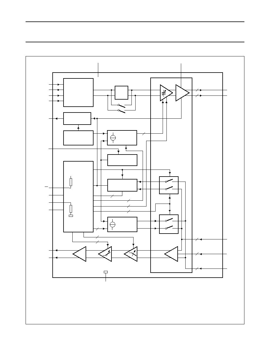
Figure 1 shows the block diagram of the device.
4
ORDERING INFORMATION
TYPE
NUMBER
PACKAGE
NAME
DESCRIPTION
VERSION
TDA5153X
-
naked die
-
TDA5153AG;
TDA5153BG
LQFP48
plastic low profile quad flat package; 48 leads; body 7
◊
7
◊
1.4 mm
SOT313-2

1997 Jul 02
4
Philips Semiconductors
Preliminary specification
Pre-amplifier for Hard Disk Drive (HDD)
with MR-read/inductive write heads
TDA5153
5
QUICK REFERENCE DATA
SYMBOL
PARAMETER
CONDITIONS
MIN.
TYP.
MAX.
UNIT
V
CC
supply voltage
4.5
5.0
5.5
V
V
CC(WD)
write drivers supply voltage
V
CC
8.0
8.8
V
F
noise figure
R
MR
= 28
; I
MR
= 10 mA;
T
amb
= 25
∞
C; f = 20 MHz
-
3.0
3.2
dB
V
nir
input referred noise voltage; see
note 3 in Chapter 13
R
MR
= 28
; I
MR
= 10 mA;
T
amb
= 25
∞
C; f = 20 MHz
-
0.9
1.0
nV/
Hz
G
v(dif)
differential voltage gain
from head inputs to RDx, RDy;
R
MR
= 28
; I
MR
= 10 mA
d4 = logic 0
-
160
-
d4 = logic 1
-
226
-
B
-
3 db
-
3 dB frequency bandwidth
upper bandwidth without gain
boost (4 nH lead inductance)
-
220
-
MHz
CMRR
common mode rejection ratio;
R
MR
mismatch <5%
I
MR
= 10 mA; f < 1 MHz
-
45
-
dB
I
MR
= 10 mA; f < 100 MHz
-
25
-
dB
PSRR
power supply rejection ratio
(input referred);
R
MR
mismatch <5%
f < 1 MHz
-
80
-
dB
f < 100 MHz
-
50
-
dB
t
r
, t
f
rise/fall times (10% to 90%)
L
h
= 150 nH; I
WR
= 35 mA;
f = 20 MHz
V
CC(WD)
= 8.0 V
-
-
1.8
ns
V
CC(WD)
= 6.5 V
-
-
2.1
ns
I
MR(PR)
programming MR bias current
R
ext
= 10 k
5
-
20.5
mA
I
WR(PR)(b-p)
programming write current
range (base-to-peak)
R
ext
= 10 k
20
-
51
mA
f
SCLK
serial interface clock rate
-
-
25
MHz
1997 Jul 02
5
Philips Semiconductors
Preliminary specification
Pre-amplifier for Hard Disk Drive (HDD)
with MR-read/inductive write heads
TDA5153
6
BLOCK DIAGRAM
Fig.1 Block diagram.
handbook, full pagewidth
MGK422
SERIAL
INTERFACE
WRITE DRIVER
INPUT
HEAD UNSAFE
INDICATOR
FF
VOLTAGE
REFERENCE
3
5
4
5
2
7
20 k
4
5
6
12
9
10
1
3
4
4
WRITE DRIVER
AND
READ PREAMP
(6
◊
)
(3)
TDA5153
head select
WRITE
CURRENT
SOURCE
LOW SUPPLY
VOLTAGE
INDICATOR
VCC(WD)
(5 to 8 V)
nWy
nWx
nRy
nGND
nRx
GND n
8, 13
18
(2)
, 23, 29,
36, 42, 47
(2)
17
(2)
, 22, 28,
35, 41, 46
(2)
16
(2)
, 21, 27,
34, 40, 45
(2)
15
(2)
, 20, 26,
33, 39, 44
(2)
14
(2)
, 19, 25,
32, 38, 43
(2)
6
(3)
6
(3)
6
(3)
6
(3)
6
(3)
6
(3)
6
(3)
48
VCC
11
RDy
RDx
Rext
SDATA
SEN
SCLK
WDly
WDlx
TAS
DETECTOR
IWDly
(1)
IWDlx
(1)
HUS
R/W
+
VCC
RMR
CURRENT
SOURCE
Pin numbers correspond to TDA5153AG and TDA5153BG only. See Fig.3 and Chapter 7 for pinning of TDA5153X.
(1) Only available on naked die.
(2) Absent on TDA5153BG (4 channel version).
(3) 4 on TDA5153BG.
1997 Jul 02
6
Philips Semiconductors
Preliminary specification
Pre-amplifier for Hard Disk Drive (HDD)
with MR-read/inductive write heads
TDA5153
7
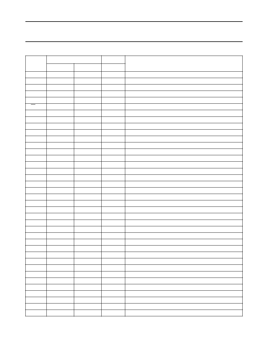
PINNING
SYMBOL
PIN
PAD
DESCRIPTION
TDA5153AG TDA5153BG TDA5153X
HUS
1
1
1
head unsafe output
WDIx
2
2
2
write data input (differential; voltage input)
WDIy
3
3
3
write data input (differential; voltage input)
IWDIx
-
-
4
write data input (differential; current input)
IWDIy
-
-
5
write data input (differential; current input)
R/W
4
4
6
read/write (read = HIGH; write = LOW)
SEN
5
5
7
serial bus enable
SDATA
6
6
8
serial bus data
SCLK
7
7
9
serial bus clock
GND1
8
8
10
ground connection 1
RDx
9
9
11
read data output (differential x
-
y)
RDy
10
10
12
read data output (differential x
-
y)
GND3
-
-
13
ground connection 3
V
CC
11
11
14
supply voltage
R
ext
12
12
15
10 k
external resistor
GND2
13
13
16
ground connection 2
0Wx
14
-
17
inductive write head connection for head H0 (differential x
-
y)
0Wy
15
-
18
inductive write head connection for head H0 (differential x
-
y)
0Rx
16
-
19
MR-read head connection for head H0 (differential x
-
y)
0GND
17
-
20
ground connection for head H0
0Ry
18
-
21
MR-read head connection for head H0 (differential x
-
y)
n.c.
-
14
-
not connected
n.c.
-
15
-
not connected
n.c.
-
16
-
not connected
n.c.
-
17
-
not connected
n.c.
-
18
-
not connected
1Wx
19
19
22
inductive write head connection for head H1 (differential x
-
y)
1Wy
20
20
23
inductive write head connection for head H1 (differential x
-
y)
1Rx
21
21
24
MR-read head connection for head H1 (differential x
-
y)
1GND
22
22
25
ground connection for head H1
1Ry
23
23
26
MR-read head connection for head H1 (differential x
-
y)
n.c.
24
24
-
not connected
2Wx
25
25
27
inductive write head connection for head H2 (differential x
-
y)
2Wy
26
26
28
inductive write head connection for head H2 (differential x
-
y)
2Rx
27
27
29
MR-read head connection for head H2 (differential x
-
y)
2GND
28
28
30
ground connection for head H2
2Ry
29
29
31
MR-read head connection for head H2 (differential x
-
y)
n.c.
30
30
-
not connected

1997 Jul 02
7
Philips Semiconductors
Preliminary specification
Pre-amplifier for Hard Disk Drive (HDD)
with MR-read/inductive write heads
TDA5153
n.c.
31
31
-
not connected
3Wx
32
32
32
inductive write head connection for head H3 (differential x
-
y)
3Wy
33
33
33
inductive write head connection for head H3 (differential x
-
y)
3Rx
34
34
34
MR-read head connection for head H3 (differential x
-
y)
3GND
35
35
35
ground connection for head H3
3Ry
36
36
36
MR-read head connection for head H3 (differential x
-
y)
n.c.
37
37
-
not connected
4Wx
38
38
37
inductive write head connection for head H4 (differential x
-
y)
4Wy
39
39
38
inductive write head connection for head H4 (differential x
-
y)
4Rx
40
40
39
MR-read head connection for head H4 (differential x
-
y)
4GND
41
41
40
ground connection for head H4
4Ry
42
42
41
MR-read head connection for head H4 (differential x
-
y)
5Wx
43
-
42
inductive write head connection for head H5 (differential x
-
y)
5Wy
44
-
43
inductive write head connection for head H5 (differential x
-
y)
5Rx
45
-
44
MR-read head connection for head H5 (differential x
-
y);
5GND
46
-
45
ground connection for head H5
5Ry
47
-
46
MR-read head connection for head H5 (differential x
-
y)
n.c.
-
43
-
not connected
n.c.
-
44
-
not connected
n.c.
-
45
-
not connected
n.c.
-
46
-
not connected
n.c.
-
47
-
not connected
V
CC(WD)
48
48
47
supply voltage for the write drivers
GND4
-
-
48
ground connection 4
SYMBOL
PIN
PAD
DESCRIPTION
TDA5153AG TDA5153BG TDA5153X

1997 Jul 02
8
Philips Semiconductors
Preliminary specification
Pre-amplifier for Hard Disk Drive (HDD)
with MR-read/inductive write heads
TDA5153
Fig.2 Pin configurations.
handbook, full pagewidth
1
2
3
4
5
6
7
8
9
10
11
36
35
34
33
32
31
30
29
28
27
26
13
14
15
16
17
18
19
20
21
22
23
48
47
46
45
44
43
42
41
40
39
38
12
24
37
25
TDA5153AG
MGK424
3Ry
3GND
3Rx
3Wy
n.c.
n.c.
2Ry
2GND
2Rx
2Wy
2Wx
3Wx
5Ry
5GND
5Rx
5Wy
5Wx
4Ry
4Rx
4Wy
4Wx
n.c.
V
CC(WD)
4GND
HUS
GND1
RDx
VCC
Rext
RDy
0Wx
0Wy
0Rx
0GND
0Ry
1Wx
1Wy
1GND
1Ry
n.c.
GND2
1Rx
WDIx
WDIy
SEN
SDATA
SCLK
R/W
handbook, full pagewidth
1
2
3
4
5
6
7
8
9
10
11
36
35
34
33
32
31
30
29
28
27
26
13
14
15
16
17
18
19
20
21
22
23
48
47
46
45
44
43
42
41
40
39
38
12
24
37
25
TDA5153BG
MGK420
3Ry
3GND
3Rx
3Wy
n.c.
n.c.
2Ry
2GND
2Rx
2Wy
2Wx
3Wx
n.c.
n.c.
n.c.
n.c.
n.c.
4Ry
4Rx
4Wy
4Wx
n.c.
V
CC(WD)
4GND
HUS
GND1
RDx
VCC
Rext
RDy
n.c.
n.c.
n.c.
n.c.
n.c.
1Wx
1Wy
1GND
1Ry
n.c.
GND2
1Rx
WDIx
WDIy
R/W
SEN
SDATA
SCLK

1997 Jul 02
9
Philips Semiconductors
Preliminary specification
Pre-amplifier for Hard Disk Drive (HDD)
with MR-read/inductive write heads
TDA5153
Fig.3 TDA5153X pad configuration.
handbook, full pagewidth
HUS
48
1
2
3
4
5
6
7
8
9
10
11
12
13
14
16
17
18
19
20
21
22
23
24
25
26
47
46
45
44
43
42
41
40
39
38
37
27
28
29
30
31
32
33
34
35
36
15
GND4
GND1
RDx
VCC
Rext
RDy
GND3
MGK421
WDIx
IWDIx
IWDIy
WDIy
SEN
R/W
SDATA
SCLK
0Wx
0Wy
0Rx
0GND
0Ry
1Wx
1Wy
1GND
1Ry
GND2
1Rx
TDA5153X
5Ry
5GND
5Rx
5Wy
5Wx
4Ry
4Rx
4Wy
4Wx
V
CC(WD)
4GND
3Ry
3GND
3Rx
3Wy
3Wx
2Ry
2GND
2Rx
2Wy
2Wx

1997 Jul 02
10
Philips Semiconductors
Preliminary specification
Pre-amplifier for Hard Disk Drive (HDD)
with MR-read/inductive write heads
TDA5153
8
FUNCTIONAL DESCRIPTION
8.1
Read mode
The read mode disables the write circuitry to save power
while reading. The read circuitry is de-activated for write,
sleep and standby modes. The read circuitry may also be
biased during write mode to shorten transients.
The selected head is connected to a multiplexed low-noise
read amplifier. The read amplifier has low-impedance
inputs nRx and nRy (n is the number of the head) and
low-impedance outputs RDx and RDy. The signal polarity
is non-inverting from x and y inputs to x and y outputs.
Ambient magnetic fields at the MR elements result in a
relative change in MR resistance
This change produces a current variation
,
where I
MR
is the bias current in the MR element.
The current variation is amplified to form the read data
output signal voltage, which is available at RDx
-
RDy.
AC coupling between MR elements and amplifier stages
prevents the amplifier input stages from overload by DC
voltages across the MR elements. A fast settling
procedure shortens DC settling transients.
An on-chip generated stable temperature reference
voltage (1.32 V), available at the R
ext
pin, is dropped
across an external resistor (10 k
) to form a global
reference current for the write and the MR bias currents.
The MR bias current DACs are programmed through the
serial interface according to the following formula
(in mA), where d4 to d0 are bits (either logic 0 or logic 1).
At power-up, all bits are set to logic 0, which results in a
default MR current of 5 mA. The adjustable range of the
MR currents is 5 mA to 20.5 mA. The MR bias currents are
equal for the two stripes of each head. The gain amplifier
is 1-bit programmable. The amplifier gain can be set to its
nominal value or to the nominal value +3 dB.
8.2
Write mode
To minimize power dissipation, the read circuitry may be
disabled in write mode. The write circuitry is disabled in
R
MR
R
MR
----------------
I
MR
I
MR
=
R
MR
R
MR
----------------
◊
I
MR
10 k
2 R
ext
------------------- 10
16 d4
8 d3
4 d2
2 d1
d0
+
+
+
+
+
(
)
=
read, sleep and standby modes. In write mode, a
programmable current is forced through the selected two
terminals inductive write head. The push-pull output
drivers yield near rail-to-rail voltage swing for fast current
polarity switching.
The differential write data input WDIx
-
WDIy is PECL
(Positive Emitter Coupled Logic) compatible. The write
data flip-flop can either be used or passed-by. In the case
that the write data flip-flop is used, current polarity is
toggled at the falling edges of the V
data
= V
WDIx
-
V
WDIy
.
Switching to Write Mode initializes the data flip-flop so that
the write current flows in the write head from x to y. In the
case that the write data flip-flop is not used, the signal
polarity is non-inverting from x and y inputs to x and y
outputs.
The write current magnitude is controlled through on-chip
DACs. The write current is defined as follows:
(in mA) where d4 to d0 are bits (either logic 0 or logic 1).
The adjustable range of the write current is 20 mA to
51 mA. At power-up, the default values
d4 = d3 = d2 = d1 = d0 = logic 0 are initialized,
corresponding to I
WR
= 20 mA. I
WR
is the current provided
by the write drivers: the current in the write coil and in the
damping resistor together. The static current in the write
coil is
,
where R
h
is the resistance of the coil including leads and
R
d
is the damping resistor.
8.3
Sleep mode
In sleep mode, the device is accessible via the serial
interface. All circuits are inactive, except the circuits of the
CMOS serial interface and the circuit which forces the data
registers to their default values at power-up and which
fixes the DC level of RDx
-
RDy (required when operating
with more than one amplifier). Typical static current
consumption is
-
30
µ
A. Dynamic current consumption
during operation of the serial interface in the sleep mode
and owing to external activity at the inputs to the serial
interface is not included. In all modes including the sleep
mode, data registers can be programmed. Sleep is the
default mode at power-up. Switching to other modes takes
less than 0.1 ms.
I
WR
10 k
R
ext
---------------- 20
16 d4
8 d3
4 d2
2 d1
d0
+
+
+
+
+
(
)
=
I
WR
1
R
h
R
d
-------
+
-----------------

1997 Jul 02
11
Philips Semiconductors
Preliminary specification
Pre-amplifier for Hard Disk Drive (HDD)
with MR-read/inductive write heads
TDA5153
8.4
Standby mode
The circuit can be put in standby mode using the serial
interface. In standby mode, typical DC current
consumption is 330
µ
A. Transients from standby mode to
active mode are two orders of magnitude shorter than from
sleep mode to active mode. This is important in the case
of cylinder mode operation with multiple amplifiers.
All amplifiers can operate from standby mode and all head
switch times can be kept just as short as in the case of
operation with a single amplifier. Head switching times are
summarized in the switching characteristics.
8.5
Active mode
Active mode is either read mode or write mode depending
on the R/W pin.
8.6
Bi-directional serial interface
The serial interface is used for programming of the device
and for reading of status information. 16 bits (8 bits for
data and 8 for address) are used to program the device.
The serial interface requires 3 pins: SDATA, SCLK and
SEN. These pins (and R/W) are CMOS inputs. The logic
input R/W has an internal 20 k
pull-up resistor and the
SEN logic input has an internal 20 k
pull-down resistor.
Thus, in case the SEN line is opened, no data will be
registered and in case the R/W line is opened, the device
will never be in write mode.
SDATA: serial data; bi-directional data interface. In all
circumstances, the LSB is transmitted first.
SCLK: serial clock; 25 MHz clock frequency.
SEN: serial enable; data transfer takes place when SEN is
HIGH. When SEN is LOW, data and clock signals are
prohibited from entering the circuit.
Three phases in the communication are distinguishable:
addressing, programming and reading. Each
communication sequence starts with an addressing
phase, followed by either a programming phase or a
reading phase.
8.7
Addressing
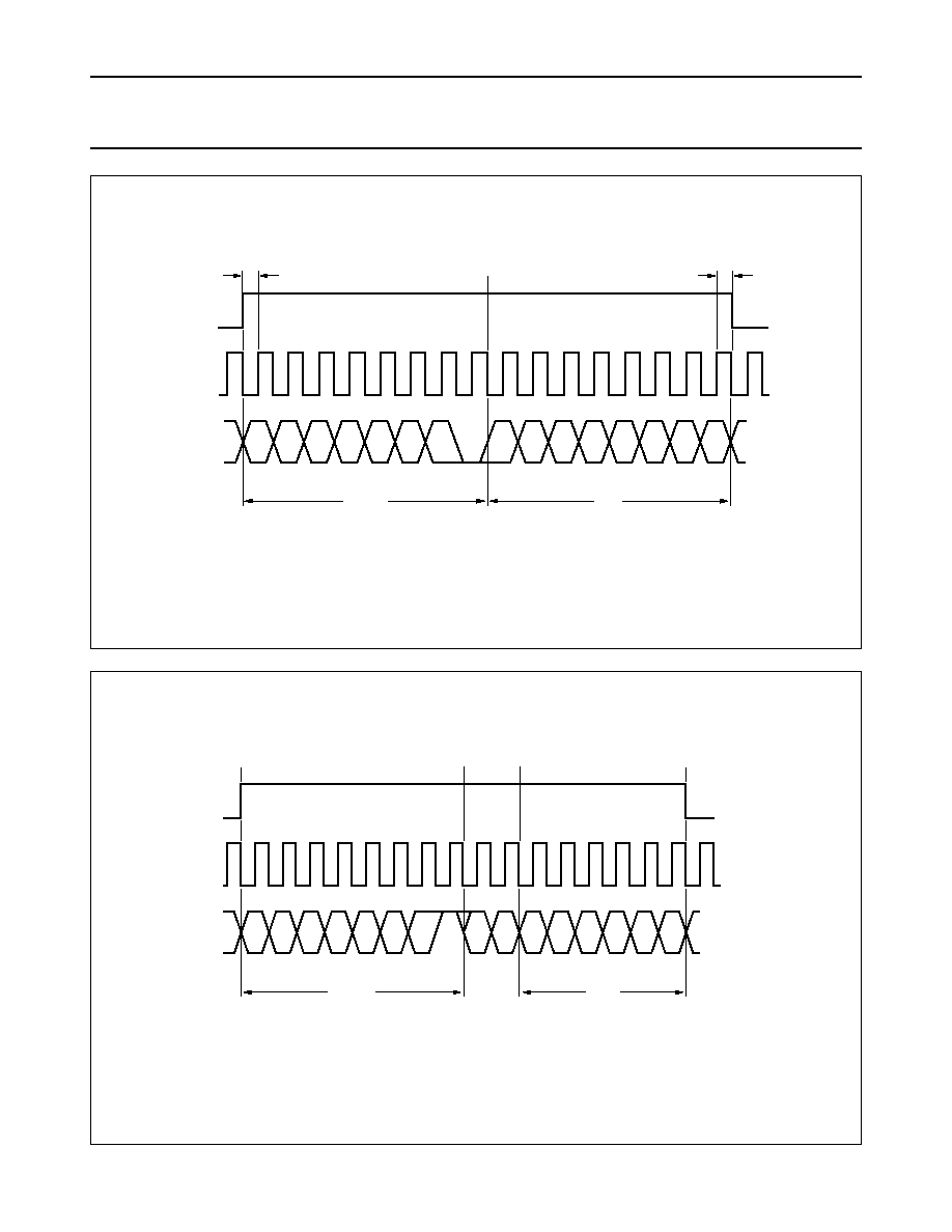
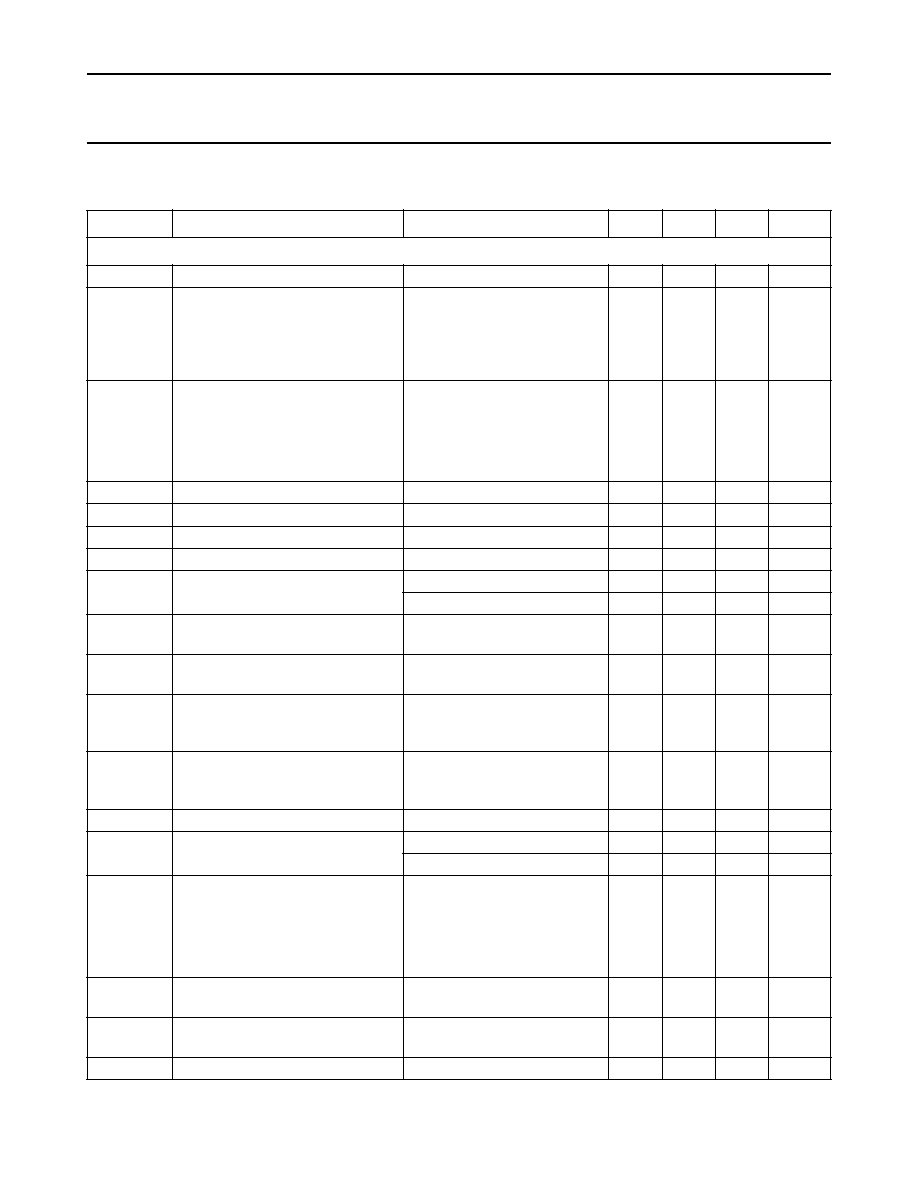
When SEN goes HIGH, bits are latched in at rising edges
of SCLK. The first eight bits a7 to a0, starting with a0, are
shifted serially into an address register. If SEN goes LOW
before 16 bits have been received, the operation is
ignored. When more than 16 bits (address and data) are
latched in before SEN goes LOW, the first 8 bits are
interpreted as an address and the last 8 bits as data.
SEN should go HIGH at least 5 ns before the first rising
edge of SCLK. Data should be valid at least 5 ns before
and after a rising edge of SCLK. The bits a7 to a4
constitute the register address.To validate the
communication with the preamplifier, bits a1, a2 and a3
have to be programmed as (1, 0, 0).
If bit a0 = logic 0, a programming sequence starts.
If bit a0 = logic 1, reading data from the pre-amplifier can
start.
8.8
Programming data
If a0 = logic 0, the last eight bits d7 to d0 before SEN goes
LOW are shifted into an input register. Bits d6 and d7 are
don't care. When SEN goes LOW, the communication
sequence is ended and the data in the input register is
copied in parallel to the data register that corresponds to
the decoded address a7 to a4. SEN should go LOW at
least 5 ns after the last rising edge of SCLK.
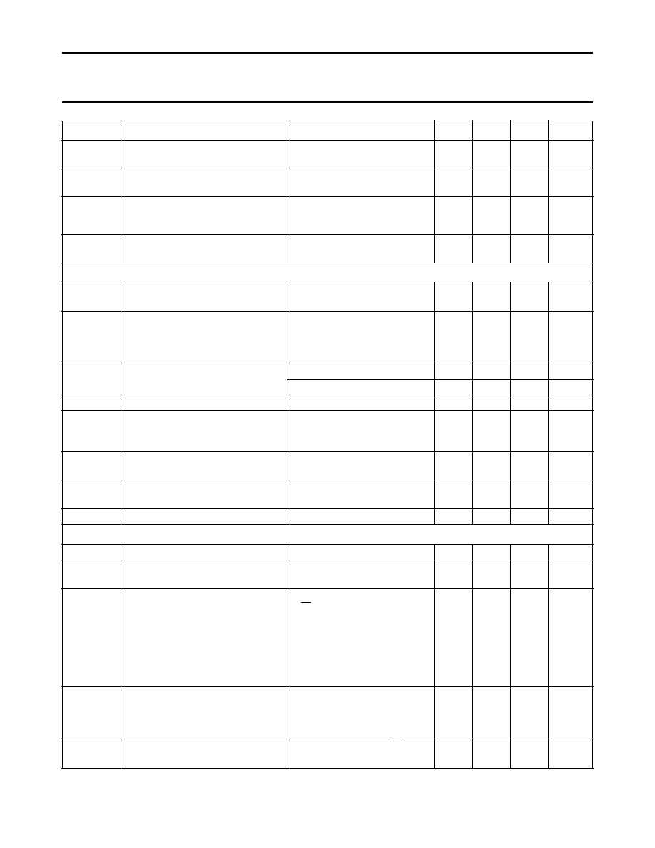
8.9
Reading data
Immediately after the IC detects that a0 = logic 1, data
from the data register (address a7 to a4) is copied in
parallel to the input register. Two wait clock cycles must
follow before the controller can start inputting data. At the
first falling edge of SCLK after the 2 wait rising edges of
SCLK, the LSB d0 is placed on SDATA line followed by d1
at the next falling edge of SCLK etc. If SEN goes LOW
before 8 address bits (a7 to a0) have been detected, the
communication is ignored.
1997 Jul 02
12
Philips Semiconductors
Preliminary specification
Pre-amplifier for Hard Disk Drive (HDD)
with MR-read/inductive write heads
TDA5153
Fig.4 Timing diagram of the serial interface operation; writing sequence (a0 = 0).
handbook, full pagewidth
MGK423
address
data
,
,
,,
,,
0
d0
a1
d1
a2
d2
a3
d3
a4
d4
a5
d5
a6
a7
d6
d7
SCLK
SDATA
SEN
>
5 ns
>
5 ns
Fig.5 Timing diagram of the serial interface operation; reading sequence (a0 = 1).
,,
,,
,,
,,
,,
,,
handbook, full pagewidth
address
data
wait
cycles
1
d0
a1
d1
a2
d2
a3
d3
a4
d4
a5
d5
a6
a7
SCLK
SDATA
SEN
MGK419

1997 Jul 02
13
Philips Semiconductors
Preliminary specification
Pre-amplifier for Hard Disk Drive (HDD)
with MR-read/inductive write heads
TDA5153
8.10
Operation of the serial interface
8.10.1
C
ONFIGURATION
d0
By default (d0 = logic 0), write data passes from the
write data input via the data flip-flop to the write driver.
The write driver toggles the current in the head at the
falling edges of
When d0 = logic 1, the flip-flop is not used. The signal
polarity is non-inverting from WDIx and WDIy to Wx and
Wy.
d1
By default (d1 = logic 0) the pre-amplifier senses PECL
write signals at WDIx and WDIy. d1 should remain
logic 0.
d2
By default, (d2 = logic 0) the write current is inhibited
under low supply voltage conditions. The write current
inhibit is made inactive by programming d2 to logic 1.
d3
By default (d3 = logic 0), in write mode low supply
voltage, open head, and other conditions are monitored
and flagged at HUS. If d3 = logic 1, HUS is LOW in write
mode and HIGH in read mode.
d4
The amplifier read gain may be programmed in the
configuration register. By default (d4 = logic 0), the read
gain is typically 160 with R
MR
= 28
. If d4 = logic 1, the
read amplifier typical gain is 3 dB higher (i.e. 226 if
R
MR
= 28
).
d5
In order to minimize the write-to-read recovery times,
the first stage of the read amplifier may be kept biased
during write mode. By default, (d5 = logic 0) the read
amplifier is powered-down during write mode, and the
fast settling procedure is activated after write-to-read
switching. If d5 = logic 1 the read amplifier is kept biased
during write mode, and the fast settling procedure still
occurs if the head is changed or the MR current is
re-programmed.
8.10.2
P
OWER CONTROL
By default d0 = d1 = logic 0, the pre-amplifier powers-up in
sleep mode. If d1 = logic 0, d0 = logic 1 or d1 = logic 1,
d0 = logic 0 the circuit goes in standby mode.
V
data
V
WDIx
V
WDIy
≠
2
--------------------------------------
=
If d1 = d0 = logic 1, the circuit goes in active mode, (read
or write mode depending on the R/W input).
8.10.3
H
EAD SELECT
d2, d1 and d0 are used to select head H0 to H5 for the
6 channel version and to select head H1 to H4 for the
4 channel version.
8.10.4
S
ERVO WRITE
The circuit is prepared for servo writing. However, the chip
will not be guaranteed.
8.10.5
T
EST
d2 = d1 = d0 = logic 0. The circuit is not in test mode. This
is the default situation.
8.10.5.1
MR head test
d2 = logic 0, d1 = logic 0, d0 = logic 1. In read mode, the
voltages at Rx and Ry (at the top of the MR elements) of
the selected head are fed to RDx and RDy outputs. By
measuring the output voltages single-ended at two
different I
MR
currents, the MR resistance can be accurately
measured according to the following formula:
for the x side for instance.
Open head and head short-circuited to ground conditions
can therefore be detected.
d2 = logic 0, d1 = logic 1, d0 = logic 0. Same as before,
with the difference that I
MR2
is fixed to a minimum constant
value of 5 mA. Measuring in the same way as above with
I
MR1
> 5 mA, enables the detection of MR elements
connected together.
8.10.5.2
Temperature monitor
d2 = logic 0, d1 = logic 1, d0 = logic 1. The temperature
monitor voltages are connected to RDx and RDy. The
output differential voltage depends on the temperature
according to:
,
The temperature may be measured with a typical precision
of 5
∞
C.
R
MRx
V
RDx1
V
RDx2
≠
I
MRx1
I
MRx2
≠
---------------------------------------
=
dV
0.00364
≠
T
1.7
+
◊
=
0
T
140
∞
C
< <

1997 Jul 02
14
Philips Semiconductors
Preliminary specification
Pre-amplifier for Hard Disk Drive (HDD)
with MR-read/inductive write heads
TDA5153
8.10.5.3
Thermal asperity detector
d2 = logic 1, d1 = don't care, d0 = either logic or 1. Unlike
the above tests, the thermal asperity detection does not
use the RDx to RDy outputs. Thus, the reader is fully
operational. In case a thermal asperity is detected, it is
flagged at the HUS pin.
The threshold voltage for the thermal asperity detection is
2-bit programmable. These 2 bits consist of d0 (LSB) of
the test mode register (address = 0XXX0110), as the
MSB, and b2 of the compensation register
(address = 0XXX0111).
,
where d0 is d0 of test mode register and b2 is d2 of
capacitor compensation register.
8.10.6
W
RITE AMPLIFIER PROGRAMMABLE CAPACITORS
By default (d2 = d1 = d0 = logic 0) the programmable
capacitors are zero. These capacitors are used to improve
the performance of the write amplifier according to the
write amplifier output load.
8.10.7
H
IGH FREQUENCY GAIN ATTENUATOR POLE
REGISTER
By default (d3 = d2 = d1 = d0 = logic 0), the high
frequency gain attenuator is not active. The gain
V
th
210
560 d0
280 b2
+
+
(
) µ
V
=
attenuator provides a pole which limits the bandwidth and
reduces the high-frequency noise. The HF pole can be
used in combination with the HF zero in order to boost the
HF gain locally and yet limit the very high frequency noise
enhancement.
8.10.8
H
IGH FREQUENCY GAIN BOOST REGISTER
By default (d3 = d2 = d1 = d0 = logic 0), the high
frequency gain boost is not active. The gain boost provides
a zero which allows to optimize the bandwidth of the read
amplifier and to correct for attenuation caused by series
inductances in the leads between the MR-heads and the
read amplifier inputs.
8.10.9
S
ETTLE PULSE
By default (d2 = d1 = d0 = logic 0) the settle pulse has a
nominal duration of 3
µ
s. Its value can be programmed
from 2.125
µ
s to 3
µ
s according to the following formula:
t
st
2
1
4 d2
2 d1
1 d0
1
+
+
+
(
)
--------------------------------------------------------------------------
µ
s
+
=
8.10.10 A
DDRESS REGISTERS
; note 1
A7 A6 A5 A4 A3 A2 A1 A0
DESCRIPTION
0
0
0
0
0
0
1
0
configuration register:
d0 = 0: use data flip-flop; d0 = 1: by-pass data flip-flop
d1 = 0: the WDI inputs are PECL levels; d1 = 1: invalid
d2 = 0: write current inhibit active; d2 = 1: write current inhibit inactive
read mode: d3 = 0: HUS active; d3 = 1: HUS HIGH
write mode: d3 = 0: HUS active; d3 = 1: HUS LOW
d4 = 0: read gain nominal; d4 = 1: read gain nominal + 3 dB
d5 = 0: read amplifier OFF during write mode; d5 = 1: read amplifier ON
during write mode
0
0
0
1
0
0
1
0
power control register:
(d1, d0) = (0, 0): sleep mode
(d1, d0) = (1, 0) or (0, 1): standby mode
(d1, d0) = (1, 1): active mode (write or read)
0
0
1
0
0
0
1
0
head select register:
6 channels: (d2,d1,d0) = (0,0,0) to (1,0,1): H0 to H5
4 channels: (d2,d1,d0) = (0, 0, 1) to (1, 0, 0): H1 to H4

1997 Jul 02
15
Philips Semiconductors
Preliminary specification
Pre-amplifier for Hard Disk Drive (HDD)
with MR-read/inductive write heads
TDA5153
Notes
1. Not used bits in the registers (indicated by X) are don't care. Default data, initialized at power-up, is zero in all
registers. For V
CC
< 2.5 V, the register contents are not guaranteed.
2. V
th
programming uses both test mode register and compensation capacitor register. d0 in the formula above is the
LSB of the test mode register and b2 is the data bit d2 of the compensation register.
0
0
1
1
0
0
1
0
MR current DAC register:
0
1
0
0
0
0
1
0
write current DAC register:
0
1
0
1
0
0
1
0
servo write register:
(d0, d1) = (0, 0) = one head
(d0, d1) = (1, 1) = all heads
0
1
1
0
0
0
1
0
test mode register:
(d2,d1,d0) = (0,0,0) = not in test mode
(d2,d1,d0) = (0,0,1) = read head test (I
MR1
= I
MR2
)
(d2,d1,d0) = (0,1,0) = read head test (I
MR2
= 5 mA fixed)
(d2,d1,d0) = (0,1,1) = temperature monitor
(d2,d1,d0) = (1, X, d0) = thermal asperity detection
, see note 2
0
1
1
1
0
0
1
0
compensation capacitor register:
equivalent differential capacitance:
1
0
0
0
0
0
1
0
high frequency gain attenuator register:
nominal pole frequency:
1
0
0
1
0
0
1
0
high-frequency gain boost register:
nominal zero frequency:
1
0
1
0
0
0
1
0
settle time register:
settle time:
1
1
1
1
0
0
1
1
chip ID register:
, d3 to d0 are preset to (0, 0, 1, 1)
a7
a6
a5
a4
0
0
1
1
when a0 = 1, data from the register with address a7 to a4 is read out on
SDATA
A7 A6 A5 A4 A3 A2 A1 A0
DESCRIPTION
I
MR
0.5
10 k
R
ext
----------------
◊
10
16 d4
8 d3
4 d2
2 d1
1 d0
+
+
+
+
+
(
)
mA
◊
=
I
WR
10 k
R
ext
----------------
20
16 d4
8 d3
4 d2
2 d1
1 d0
+
+
+
+
+
(
)
mA
◊
=
V
th
210
560 d0
280 b2
+
+
(
) µ
V
=
4 d2
2 d1
1 d0
+
+
(
)
2 pF
◊
800 MHz
8 d3
4 d2
2 d1
1 d0
+
+
+
-------------------------------------------------------------------------------
800 MHz
8 d3
4 d2
2 d1
1 d0
+
+
+
-------------------------------------------------------------------------------
t
st
2
1
4 d2
2 d1
1 d0
1
+
+
+
(
)
--------------------------------------------------------------------------
µ
s
+
=
ID
8 d3
4 d2
2 d1
1 d0
+
+
+
=
1997 Jul 02
16
Philips Semiconductors
Preliminary specification
Pre-amplifier for Hard Disk Drive (HDD)
with MR-read/inductive write heads
TDA5153
8.11
Head unsafe
The HUS pin is an open-collector output. Consequently,
when the pin is not connected to an external pull-up
resistor, HUS is LOW. HUS pins can be connected
together in case of operation with more than one amplifier.
It is used to detect abnormal/unexpected operation.
Sleep mode: HUS is HIGH, to permit working with more
than one amplifier.
Standby mode: HUS is HIGH, to permit working with
more than one amplifier.
Read mode:
∑
if in the configuration register d3 = 1, HUS is HIGH
∑
if in the configuration register d3 = 0, HUS goes LOW
for:
≠ R
ext
pin open, short-circuited to ground or to V
CC
(read current too low or too high)
≠ Low V
CC
and V
CC(WD)
conditions. A low supply
voltage detector is placed close to the V
CC
and
V
CC(WD)
pins.
Detection of low V
CC
(main general supply): a V
CC
supply
voltage below 4.0 V
±
5% is flagged to the HUS pin.
The voltage detection range is then 4.2 to 3.8 V with an
hysteresis of 110 mV
±
10%. Detection of low V
CC(WD)
(writer dedicated supply): a fault will be flagged at HUS pin
if V
CC(WD)
drops 0.8 V
±
10% below V
CC
. One must be
aware that such a detection is only aimed to warn for a
catastrophic situation. Indeed, V
CC(WD)
should never be
below V
CC
.
Test mode: HUS is HIGH except when the TAS detector
is ON. If a thermal asperity is detected, HUS goes LOW.
Servo write mode: HUS is LOW
Write mode:
∑
if in the configuration register d3 = 1, HUS is LOW
∑
if in the configuration register d3 = 0, HUS goes HIGH
for: the write current may be inhibited if d1 = 0 in the
configuration register.
≠ R
ext
pin open, short-circuited to ground or to V
CC
(write current too low or too high)
≠ Write data input frequency too low (WDIx
-
WDIy)
≠ Write head Wx
-
Wy open, Wx or Wy short-circuited
to ground (switching to write mode makes HUS LOW;
after the transient the HUS detection circuitry is
activated; the target for the head-open detect time is
15 ns)
≠ Write-head still left biased while not selected
≠ Low V
CC
and V
CC(WD)
conditions (write current inhibit
can be active or inactive).
The same detector is used for read and write mode. HUS
goes LOW again between 0.5 and 1
µ
s after the last
unsafe condition was detected.
8.12
HUS survey
Notes
1. HUS survey: A-test mode = analog test mode.
2. In servo mode, the performance of the IC is not guaranteed.
HUS
DATA BIT D3
MODE
STATE
0
1
Sleep mode
-
-
HIGH
HIGH
Standby mode
-
-
HIGH
HIGH
Active mode
Read
Read mode
ACTIVE
HIGH
A-test mode
(1)
HIGH
HIGH
TAS mode
ACTIVE
ACTIVE
Write
Write mode
ACTIVE
LOW
A-test mode
(1)
HIGH
HIGH
Servo mode
(2)
LOW
LOW

1997 Jul 02
17
Philips Semiconductors
Preliminary specification
Pre-amplifier for Hard Disk Drive (HDD)
with MR-read/inductive write heads
TDA5153
9
LIMITING VALUES
In accordance with the Absolute Maximum Rating System (IEC 134).
10 HANDLING
Inputs and outputs are protected against electrostatic discharge in normal handling. However, to be totally safe, it is
desirable to take normal precautions appropriate to handling MOS device.
11 THERMAL CHARACTERISTICS
Note
1. The TDA5153X is shipped in naked dies. The thermal resistance depends on the flex used.
SYMBOL
PARAMETER
MIN.
MAX.
UNIT
V
CC
supply voltage
-
0.5
+6.0
V
V
CC(WD)
write driver supply voltage
-
0.5
+9.5
V
V
IL
LOW level digital input voltage
-
0.5
+5.5
V
V
IH
HIGH level digital input voltage
-
0.5
+5.5
V
V
n1
voltage on all pins except V
CC
, read inputs nRx, nRy and
write outputs nWx, nWy (n = 0 to 9)
-
0.5
+5.5
V
but not higher than
-
V
CC
+ 0.5
V
V
n2
voltage on write driver outputs nWx, nWy
-
0.5
+8.8
V
but not higher than
-
V
CC(WD)
+ 0.8 V
V
n3
voltage on read inputs nRx, nRy
-
0.5
1
V
I
nGND
current through pins nGND
-
0.1
A
T
stg
storage temperature
-
65
+150
∞
C
T
j
junction temperature
-
150
∞
C
SYMBOL
PARAMETER
CONDITION
VALUE
UNIT
R
th j-a
thermal resistance from junction to ambient
TDA5153AG, TDA5153BG
in free air
70
K/W
TDA5153X
see note 1

1997 Jul 02
18
Philips Semiconductors
Preliminary specification
Pre-amplifier for Hard Disk Drive (HDD)
with MR-read/inductive write heads
TDA5153
12 RECOMMENDED OPERATION CONDITIONS
Notes
1. A supply by-pass capacitor from V
CC
to ground or a low-pass filter may be used to optimize the PSRR.
2. The supply voltage V
CC(WD)
must never be below V
CC
in normal mode, and two diode voltages above V
CC
in servo
mode.
3. The given values should be interpreted in such a way that the single-ended voltage could swing 0.2 to 0.75 V and
that the common mode voltage should be such that for any of the two states, V
IH(max)
< V
CC
and V
IL(min)
> 1.5 V.
PECL voltage swing: a wider peak-to-peak voltage swing can be used. In that case a current will flow through the
WDI inputs. This current is approximately equal to
4. The mismatch refers to the resistance of the two stripes of the same head. This is defined as follows:
R
MR
=
R
MR1
-
R
MR2
5. These parameters depend on the head model. The values given are those used for testing.
6. The combination of maximum head resistance, lead resistance and bias current is not permitted. To avoid voltage
break-through between heads and disk, the voltage over the MR elements is limited by two diodes.
SYMBOL
PARAMETER
CONDITIONS
MIN.
TYP
MAX.
UNIT
V
CC
supply voltage range
note 1
4.5
-
5.5
V
V
CC(WD)
write driver supply voltage
note 2
V
CC
-
8.8
V
V
IH
HIGH level input voltage (CMOS)
3.5
-
V
CC
V
V
IL
LOW level input voltage (CMOS)
0
-
0.8
V
V
i(dif)(p-p)
differential input voltage
(peak-to-peak value)
note 3
0.4
0.7
1.5
V
V
IH(PECL)
HIGH level PECL input voltage
note 3
1.5
2.85
V
CC
V
V
IL(PECL)
LOW level PECL input voltage
note 3
-
2.15
-
V
T
amb
ambient temperature
0
-
70
∞
C
T
j
junction temperature
reading
-
-
110
∞
C
writing (V
CC(WD)
= 8 V)
-
-
130
∞
C
R
MR
MR element resistance
15
28
34
R
MR
R
MR
mismatch
note 4
-
-
4
L
l(tot)
total lead inductance to the head
in each lead; note 5
-
35
-
nH
R
l(tot)
total lead resistance to the head
in each lead; note 5
-
1.5
-
V
MR
voltage on top of MR elements
note 6
-
-
0.5
V
V
sig(dif)(p-p)
differential MR head input signal
(peak-to-peak value)
0.4
1
2
mV
L
wh
write head inductance
including lead; note 5
-
0.15
-
µ
H
R
wh
write head resistance
including lead; note 5
-
10
-
C
wh
write head capacitance
including lead; note 5
-
5
-
pF
R
ext
external reference resistor
-
10
-
k
I
ref
V
ref
R
ext
-----------
=
WDIx
WDIy
≠
(
)
1.4
≠
200
-----------------------------------------------------------
1997 Jul 02
19
Philips Semiconductors
Preliminary specification
Pre-amplifier for Hard Disk Drive (HDD)
with MR-read/inductive write heads
TDA5153
13 CHARACTERISTICS
V
CC
= 5.0 V; V
CC(WD)
= 8 V; V
GND
= 0 V; T
amb
= 25
∞
C; unless otherwise specified.
SYMBOL
PARAMETER
CONDITIONS
MIN.
TYP.
MAX.
UNIT
Read characteristics
I
MR
MR current adjust range
R
ext
= 10 k
; 0.5 mA steps
5
-
20.5
mA
I
MR
tolerance (excluding R
ext
)
with I
MR(PR)
= 10 mA
-
±
4
-
%
G
v(dif)
differential voltage gain; note 1
from head inputs to RDx, RDy;
R
MR
= 28
; I
MR
= 10 mA;
f = 20 MHz;
d4 = 0
-
160
-
d4 = 1
-
226
-
R
i(dif)
differential input resistance
I
MR
= 10 mA
-
13
-
C
i(dif)
differential input capacitance
-
16
-
pF
THD
total harmonic distortion
-
1
-
%
B
L
signal gain pass band edge; note 2
-
3 dB
-
-
100
kHz
B
H
signal gain pass band edge without
gain boost; note 2
-
3 dB (4 nH lead inductance)
-
220
-
MHz
-
3 dB (50 nH lead inductance)
-
170
-
MHz
F
noise figure; note 3
R
MR
= 28
; I
MR
= 10mA;
T
amb
= 25
∞
C; f = 20 MHz
-
3.0
3.2
dB
V
nir
input referred noise voltage; note 3 R
MR
= 28
; I
MR
= 10mA;
T
amb
= 25
∞
C; f = 20 MHz
-
0.9
1.0
nV/
Hz
f
B(L)
+3 dB noise low corner frequency
R
MR
= 28
; I
MR
= 10 mA;
T
amb
= 25
∞
C; no lead
inductance
-
400
kHz
f
B(H)
+3 dB noise upper corner
frequency
R
MR
= 28
; I
MR
= 10 mA;
T
amb
= 25
∞
C; no lead
inductance
-
220
MHz
cs
channel separation; note 4
unselected head
-
50
dB
PSRR
power supply rejection ratio; note 5 f < 1 MHz; I
MR
= 10 mA
-
80
dB
f < 100 MHz; I
MR
= 10 mA
-
50
dB
CMRR
common mode rejection ratio;
note 5
from nRx
-
nRy to RDx
-
RDy;
R
MR
mismatch < 5%;
I
MR
= 10 mA;
f < 1 MHz
-
45
dB
f < 100 MHz
-
25
dB
DR
rejection of SCLK and SDATA;
note 6
from SCLK, SDATA inputs to
the RDx
-
RDy outputs; note 7
-
50
dB
V
O(R)(dif)
output DC offset voltage in read
mode (differential after DC settling)
DC voltage between
RDx
-
RDy (in read mode)
-
-
±
0.2
V
Z
o(R)
output impedance in read mode
single ended
-
16
-
I
MR
I
MR(PR)
≠
I
MR(PR)
----------------------------------
1997 Jul 02
20
Philips Semiconductors
Preliminary specification
Pre-amplifier for Hard Disk Drive (HDD)
with MR-read/inductive write heads
TDA5153
I
o(max)(dif)
maximum differential output
current
-
4
-
mA
V
o(cm)
common mode output voltage in
read mode
RDx, RDy
1.0
1.5
2.0
V
common mode DC supply rejection
in read mode
-
20
-
dB
Z
o(n)(dif)
differential output impedance in
other modes (write, standby, sleep)
-
50
-
k
Write characteristics
I
WR
write current adjust range (in the
write drivers)
R
ext
= 10 k
; 1 mA steps
20
35
51
mA
I
WR
tolerance (excluding R
ext
);
I
WR(PR)
= 35 mA
-
±
7
-
%
V
s(max)(p-p)
maximum voltage swing
(peak-to-peak value)
V
CC(WD)
= 5 V
-
-
8
V
V
CC(WD)
= 8 V (differential)
-
-
13
V
R
o(dif)
differential output resistance
-
200
-
t
r
, t
f
write current rise/fall time without
flip-flop (10% to 90%); note 8
V
CC(WD)
= 8 V; L
h
= 150 nH,
R
h
= 10
; I
WR
= 35 mA;
f = 20 MHz
-
-
1.8
ns
t
as
write current asymmetry; note 9
percentage of t
r
/t
f
(t
r
, t
f
and logic asymmetry)
-
-
5
%
t
pd
propagation delay 50% of
(WDIx/WDIy) to 50% of (Wx, Wy)
write head short circuited; data
flip-flop by passed
-
-
5
ns
cs
channel separation
unselected head
-
45
-
dB
Switching characteristics
f
SCLK
serial interface clock rate
-
-
25
MHz
V
o(cm)
output common mode DC voltage
change from Read to Write modes
I
MR
= 10 mA; I
WR
= 35 mA
-
200
-
mV
t
rec(W-R)
write to read recovery time
(AC and DC settling); note 10
from 50% of the rising edge of
R/W to steady state read-back
signal: AC and DC settling at
90% (without load at
RDx
-
RDy)
read amplifier OFF: d5 = 0
-
3
4.5
µ
s
read amplifier ON: d5 = 1
-
100
150
µ
s
t
sw(R)
head switching (in read mode),
standby to read active and MR
current change recovery time;
(AC and DC settling); note 11
from falling edge of SEN to
steady state read-back signal;
(without load at RDx
-
RDy)
-
3
4.5
µ
s
t
off(R)
read amplifier off time
from falling edge of R/W to
read head inactive
-
-
50
ns
SYMBOL
PARAMETER
CONDITIONS
MIN.
TYP.
MAX.
UNIT
V
ocm
V
CC
----------------
I
WR
I
RW (PR)
≠
I
RW (PR)
------------------------------------

1997 Jul 02
21
Philips Semiconductors
Preliminary specification
Pre-amplifier for Hard Disk Drive (HDD)
with MR-read/inductive write heads
TDA5153
t
st(W)
write settle times; note 12
from 50%of the falling edge of
R/W to 90% of the steady state
write current (in Write Mode)
-
-
70
ns
t
off(W)
write amplifier off time
from rising edge of R/W to
I
WR
-programmed /10
(I
WR
= 35 mA)
-
-
50
ns
t
sw(W)
head switching (in write mode),
and standby to write head active
from falling edge of SEN to
write head active
-
50
70
ns
t
sw(S)
sleep to (and from) any other
modes
-
-
100
µ
s
DC characteristics
I
CC(R)
supply current; note 13
read mode; I
MR
= 10 mA
-
72
80
mA
I
CC(W)
supply current; note 14
write mode; I
WR
= 35 mA
from V
CC
(5 V)
-
33
41
mA
from V
CC(WD)
(5 to 8 V)
-
54
61
mA
I
DD(stb)
standby mode supply current
-
0.25
1
mA
I
DD(S)
sleep mode supply current
static
-
0.025
-
mA
V
ref
reference voltage for R
ext
-
1.32
-
V
SYMBOL
PARAMETER
CONDITIONS
MIN.
TYP.
MAX.
UNIT
Notes to the characteristics
1. The differential voltage gain depends on the MR
resistance. It can be improved by programming the
d4 bit in the configuration register using the serial
interface.
2. The gain boost implements a pole-zero combination:
The +3 dB gain boost corner frequency is
The
-
3 dB gain attenuation corner frequency is
where d3, d2, d1, d0 are bits (0, 1) to be programmed
via the Serial Interface. In practical use, the bandwidth
is limited by the inductance of the connection between
the MR heads and the pre-amplifier.
3. Noise calculation
a) Definitions: The amplifier has a low-ohmic input.
No lead resistance is taken into account. The input
referred noise voltage, excluding the noise of the
MR resistors, is defined as follows:
where G
v
is the voltage gain and V
no
is the noise
voltage at the output of the amplifier, k is the
800 MHz
8 d3
4 d2
2 d1
1 d0
+
+
+
(
)
-------------------------------------------------------------------------------------
800 MHz
8 d3
4 d2
2 d1
1 d0
+
+
+
(
)
-------------------------------------------------------------------------------------
V
nir
2
V
no
G
v
---------
2
4kT
R
MR1
R
MR2
+
(
)
◊
V
≠
=
Boltzmann constant and T is the temperature in K.
The noise figure is defined as follows:
in 1 Hz bandwidth. Note that R
MR
includes all
resistances between Rx or Ry to ground.
b) Noise figure versus I
MR
and R
MR
: Table 1 shows
the variation of the noise figure with I
MR
(mA) and
R
MR
(
).
c) Input noise voltage consideration: the input
referred noise voltage calculation can significantly
be different (from 1.0 to 0.44 nV/
Hz for instance)
by taking into account an equivalent
signal-to-noise ratio when using two MR stripes
(28
for each stripe) or one MR stripes (42 W).
It assumes that the signal coming from the head is
larger for a dual stripe head than for a single stripe
head (50% extra signal for dual stripe head).
4. The channel separation is defined by the ratio of the
gain response of the amplifier using the selected head
H(n) to the gain response of the amplifier using the
adjacent head H(n
±
1), Head H(n) being selected.
F
10
log
V
no
G
v
---------
2
4kT
R
MR1
R
MR2
+
(
)
◊
------------------------------------------------------------
◊
dB
=
1997 Jul 02
22
Philips Semiconductors
Preliminary specification
Pre-amplifier for Hard Disk Drive (HDD)
with MR-read/inductive write heads
TDA5153
5.
The PSRR (in dB) is defined as input referred ratio:
Where G
v
is the differential input to differential output
gain, and G
p
is the power supply to differential output
gain. The CMRR (in dB) is defined as input referred
ratio:
where G
v
is the differential input to differential output
gain and G
cm
is the common mode input to differential
output gain. Flex and board lay-out may affect
significantly these parameters.
6. This refers to the crosstalk from SCLK and SDATA
inputs via the read inputs to RDx
-
RDy. Two cases
can be distinguished:
a) With SEN LOW, SCLK and SDATA are prohibited
from entering the device and crosstalk is low.
b) Programming via the serial interface is done with
SEN HIGH. Then crosstalk can occur. A careful
design of the board or flex-foil is required in order
not to get crosstalk via this path.
7. A 200 mV peak-to-peak signal is applied to SCLK or
SDATA inputs at 25 MHz, and measurement is
performed at RDx
-
RDy.
PSRR
20
log
G
v
G
p
-------
◊
=
CMRR
20
log
G
v
G
cm
-----------
◊
=
8. The rise and fall times depend on the write
amplifier-write head combination. L
h
and R
h
represent
the components on the evaluation board. Parasitic
capacitances also limit the performance.
9. The write current rise/fall time asymmetry is defined by
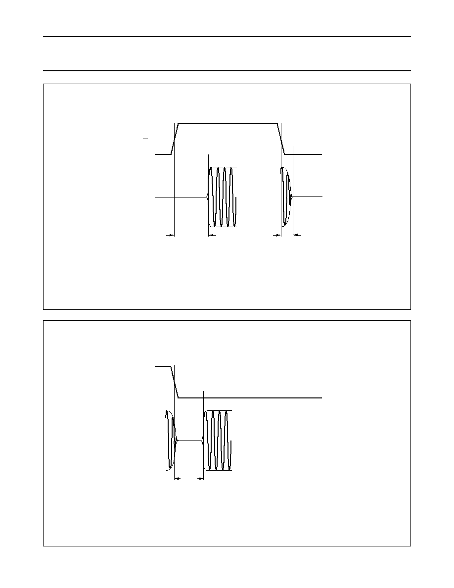
10. Write-to-read recovery time includes the write mode to
read mode switching using the R/W pin on the same
head (see Fig.6). The AC signal reaches its full
amplitude few tenth of ns after appearing at the reader
RDx and RDy outputs.
11. In read mode, the head switching, standby to read
active switching and changing MR current include fast
current settling (see Fig.7). Same note regarding the
AC signals at the reader outputs as above.
12. Write settle time includes read mode to write mode
switching using the R/W pin.
13. The typical supply current in read mode depends on
the bias current for the MR element.
14. The typical supply current in write mode also depends
on the write current.
t
r
t
f
≠
2 t
r
t
f
+
(
)
-----------------------
Table 1
Noise figure
R
MR
(
)
F (dB)
I
MR
= 7 mA
I
MR
= 10 mA
I
MR
= 15 mA
20
2.7
2.9
3.1
25
2.8
3.0
3.3
30
2.9
3.1
3.5
1997 Jul 02
23
Philips Semiconductors
Preliminary specification
Pre-amplifier for Hard Disk Drive (HDD)
with MR-read/inductive write heads
TDA5153
Fig.6 Timing diagram of the reader: write-to-read switching on the same logic head.
handbook, full pagewidth
MGG985
toff(R)
trec(W-R)
RDx-RDy
R/W
Fig.7 Timing diagram of the reader: typical head, current and standby-to-read characteristics.
handbook, full pagewidth
MGG986
tsw(R)
RDx-RDy
SEN
1997 Jul 02
24
Philips Semiconductors
Preliminary specification
Pre-amplifier for Hard Disk Drive (HDD)
with MR-read/inductive write heads
TDA5153
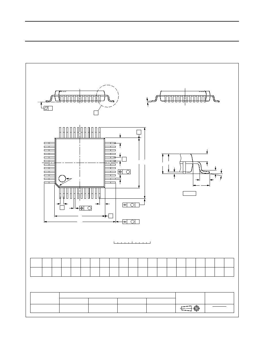
14 PACKAGE OUTLINE
UNIT
A
max.
A
1
A
2
A
3
b
p
c
E
(1)
e
H
E
L
L
p
Q
Z
y
w
v
REFERENCES
OUTLINE
VERSION
EUROPEAN
PROJECTION
ISSUE DATE
IEC
JEDEC
EIAJ
mm
1.60
0.20
0.05
1.45
1.35
0.25
0.27
0.17
0.18
0.12
7.1
6.9
0.5
9.15
8.85
0.69
0.59
0.95
0.55
7
0
o
o
0.12
0.1
0.2
1.0
DIMENSIONS (mm are the original dimensions)
Note
1. Plastic or metal protrusions of 0.25 mm maximum per side are not included.
0.75
0.45
SOT313-2
93-06-15
94-12-19
D
(1)
(1)
(1)
7.1
6.9
H
D
9.15
8.85
E
Z
0.95
0.55
D
b
p
e
E
B
12
D
H
b
p
E
H
v
M
B
D
ZD
A
Z E
e
v
M
A
1
48
37
36
25
24
13
A
1
A
L
p
Q
detail X
L
(A )
3
A
2
X
y
c
w
M
w
M
0
2.5
5 mm
scale
pin 1 index
LQFP48: plastic low profile quad flat package; 48 leads; body 7 x 7 x 1.4 mm
SOT313-2

1997 Jul 02
25
Philips Semiconductors
Preliminary specification
Pre-amplifier for Hard Disk Drive (HDD)
with MR-read/inductive write heads
TDA5153
15 SOLDERING
15.1
Introduction
There is no soldering method that is ideal for all IC
packages. Wave soldering is often preferred when
through-hole and surface mounted components are mixed
on one printed-circuit board. However, wave soldering is
not always suitable for surface mounted ICs, or for
printed-circuits with high population densities. In these
situations reflow soldering is often used.
This text gives a very brief insight to a complex technology.
A more in-depth account of soldering ICs can be found in
our
"IC Package Databook" (order code 9398 652 90011).
15.2
Reflow soldering
Reflow soldering techniques are suitable for all LQFP
packages.
Reflow soldering requires solder paste (a suspension of
fine solder particles, flux and binding agent) to be applied
to the printed-circuit board by screen printing, stencilling or
pressure-syringe dispensing before package placement.
Several techniques exist for reflowing; for example,
thermal conduction by heated belt. Dwell times vary
between 50 and 300 seconds depending on heating
method. Typical reflow temperatures range from
215 to 250
∞
C.
Preheating is necessary to dry the paste and evaporate
the binding agent. Preheating duration: 45 minutes at
45
∞
C.
15.3
Wave soldering
Wave soldering is not recommended for LQFP packages.
This is because of the likelihood of solder bridging due to
closely-spaced leads and the possibility of incomplete
solder penetration in multi-lead devices.
If wave soldering cannot be avoided, the following
conditions must be observed:
∑
A double-wave (a turbulent wave with high upward
pressure followed by a smooth laminar wave)
soldering technique should be used.
∑
The footprint must be at an angle of 45
∞
to the board
direction and must incorporate solder thieves
downstream and at the side corners.
Even with these conditions, do not consider wave
soldering LQFP packages LQFP48 (SOT313-2),
LQFP64 (SOT314-2) or LQFP80 (SOT315-1).
During placement and before soldering, the package must
be fixed with a droplet of adhesive. The adhesive can be
applied by screen printing, pin transfer or syringe
dispensing. The package can be soldered after the
adhesive is cured.
Maximum permissible solder temperature is 260
∞
C, and
maximum duration of package immersion in solder is
10 seconds, if cooled to less than 150
∞
C within
6 seconds. Typical dwell time is 4 seconds at 250
∞
C.
A mildly-activated flux will eliminate the need for removal
of corrosive residues in most applications.
15.4
Repairing soldered joints
Fix the component by first soldering two diagonally-
opposite end leads. Use only a low voltage soldering iron
(less than 24 V) applied to the flat part of the lead. Contact
time must be limited to 10 seconds at up to 300
∞
C. When
using a dedicated tool, all other leads can be soldered in
one operation within 2 to 5 seconds between
270 and 320
∞
C.
1997 Jul 02
26
Philips Semiconductors
Preliminary specification
Pre-amplifier for Hard Disk Drive (HDD)
with MR-read/inductive write heads
TDA5153
16 DEFINITIONS
17 LIFE SUPPORT APPLICATIONS
These products are not designed for use in life support appliances, devices, or systems where malfunction of these
products can reasonably be expected to result in personal injury. Philips customers using or selling these products for
use in such applications do so at their own risk and agree to fully indemnify Philips for any damages resulting from such
improper use or sale.
Data sheet status
Objective specification
This data sheet contains target or goal specifications for product development.
Preliminary specification
This data sheet contains preliminary data; supplementary data may be published later.
Product specification
This data sheet contains final product specifications.
Limiting values
Limiting values given are in accordance with the Absolute Maximum Rating System (IEC 134). Stress above one or
more of the limiting values may cause permanent damage to the device. These are stress ratings only and operation
of the device at these or at any other conditions above those given in the Characteristics sections of the specification
is not implied. Exposure to limiting values for extended periods may affect device reliability.
Application information
Where application information is given, it is advisory and does not form part of the specification.

1997 Jul 02
27
Philips Semiconductors
Preliminary specification
Pre-amplifier for Hard Disk Drive (HDD)
with MR-read/inductive write heads
TDA5153
NOTES

Internet: http://www.semiconductors.philips.com
Philips Semiconductors ≠ a worldwide company
© Philips Electronics N.V. 1997
SCA54
All rights are reserved. Reproduction in whole or in part is prohibited without the prior written consent of the copyright owner.
The information presented in this document does not form part of any quotation or contract, is believed to be accurate and reliable and may be changed
without notice. No liability will be accepted by the publisher for any consequence of its use. Publication thereof does not convey nor imply any license
under patent- or other industrial or intellectual property rights.
Netherlands: Postbus 90050, 5600 PB EINDHOVEN, Bldg. VB,
Tel. +31 40 27 82785, Fax. +31 40 27 88399
New Zealand: 2 Wagener Place, C.P.O. Box 1041, AUCKLAND,
Tel. +64 9 849 4160, Fax. +64 9 849 7811
Norway: Box 1, Manglerud 0612, OSLO,
Tel. +47 22 74 8000, Fax. +47 22 74 8341
Philippines: Philips Semiconductors Philippines Inc.,
106 Valero St. Salcedo Village, P.O. Box 2108 MCC, MAKATI,
Metro MANILA, Tel. +63 2 816 6380, Fax. +63 2 817 3474
Poland: Ul. Lukiska 10, PL 04-123 WARSZAWA,
Tel. +48 22 612 2831, Fax. +48 22 612 2327
Portugal: see Spain
Romania: see Italy
Russia: Philips Russia, Ul. Usatcheva 35A, 119048 MOSCOW,
Tel. +7 095 755 6918, Fax. +7 095 755 6919
Singapore: Lorong 1, Toa Payoh, SINGAPORE 1231,
Tel. +65 350 2538, Fax. +65 251 6500
Slovakia: see Austria
Slovenia: see Italy
South Africa: S.A. PHILIPS Pty Ltd., 195-215 Main Road Martindale,
2092 JOHANNESBURG, P.O. Box 7430 Johannesburg 2000,
Tel. +27 11 470 5911, Fax. +27 11 470 5494
South America: Rua do Rocio 220, 5th floor, Suite 51,
04552-903 S„o Paulo, S√O PAULO - SP, Brazil,
Tel. +55 11 821 2333, Fax. +55 11 829 1849
Spain: Balmes 22, 08007 BARCELONA,
Tel. +34 3 301 6312, Fax. +34 3 301 4107
Sweden: Kottbygatan 7, Akalla, S-16485 STOCKHOLM,
Tel. +46 8 632 2000, Fax. +46 8 632 2745
Switzerland: Allmendstrasse 140, CH-8027 ZÐRICH,
Tel. +41 1 488 2686, Fax. +41 1 481 7730
Taiwan: Philips Semiconductors, 6F, No. 96, Chien Kuo N. Rd., Sec. 1,
TAIPEI, Taiwan Tel. +886 2 2134 2865, Fax. +886 2 2134 2874
Thailand: PHILIPS ELECTRONICS (THAILAND) Ltd.,
209/2 Sanpavuth-Bangna Road Prakanong, BANGKOK 10260,
Tel. +66 2 745 4090, Fax. +66 2 398 0793
Turkey: Talatpasa Cad. No. 5, 80640 GÐLTEPE/ISTANBUL,
Tel. +90 212 279 2770, Fax. +90 212 282 6707
Ukraine: PHILIPS UKRAINE, 4 Patrice Lumumba str., Building B, Floor 7,
252042 KIEV, Tel. +380 44 264 2776, Fax. +380 44 268 0461
United Kingdom: Philips Semiconductors Ltd., 276 Bath Road, Hayes,
MIDDLESEX UB3 5BX, Tel. +44 181 730 5000, Fax. +44 181 754 8421
United States: 811 East Arques Avenue, SUNNYVALE, CA 94088-3409,
Tel. +1 800 234 7381
Uruguay: see South America
Vietnam: see Singapore
Yugoslavia: PHILIPS, Trg N. Pasica 5/v, 11000 BEOGRAD,
Tel. +381 11 625 344, Fax.+381 11 635 777
For all other countries apply to: Philips Semiconductors, Marketing & Sales Communications,
Building BE-p, P.O. Box 218, 5600 MD EINDHOVEN, The Netherlands, Fax. +31 40 27 24825
Argentina: see South America
Australia: 34 Waterloo Road, NORTH RYDE, NSW 2113,
Tel. +61 2 9805 4455, Fax. +61 2 9805 4466
Austria: Computerstr. 6, A-1101 WIEN, P.O. Box 213,
Tel. +43 1 60 101, Fax. +43 1 60 101 1210
Belarus: Hotel Minsk Business Center, Bld. 3, r. 1211, Volodarski Str. 6,
220050 MINSK, Tel. +375 172 200 733, Fax. +375 172 200 773
Belgium: see The Netherlands
Brazil: see South America
Bulgaria: Philips Bulgaria Ltd., Energoproject, 15th floor,
51 James Bourchier Blvd., 1407 SOFIA,
Tel. +359 2 689 211, Fax. +359 2 689 102
Canada: PHILIPS SEMICONDUCTORS/COMPONENTS,
Tel. +1 800 234 7381
China/Hong Kong: 501 Hong Kong Industrial Technology Centre,
72 Tat Chee Avenue, Kowloon Tong, HONG KONG,
Tel. +852 2319 7888, Fax. +852 2319 7700
Colombia: see South America
Czech Republic: see Austria
Denmark: Prags Boulevard 80, PB 1919, DK-2300 COPENHAGEN S,
Tel. +45 32 88 2636, Fax. +45 31 57 0044
Finland: Sinikalliontie 3, FIN-02630 ESPOO,
Tel. +358 9 615800, Fax. +358 9 61580920
France: 4 Rue du Port-aux-Vins, BP317, 92156 SURESNES Cedex,
Tel. +33 1 40 99 6161, Fax. +33 1 40 99 6427
Germany: Hammerbrookstraþe 69, D-20097 HAMBURG,
Tel. +49 40 23 53 60, Fax. +49 40 23 536 300
Greece: No. 15, 25th March Street, GR 17778 TAVROS/ATHENS,
Tel. +30 1 4894 339/239, Fax. +30 1 4814 240
Hungary: see Austria
India: Philips INDIA Ltd, Shivsagar Estate, A Block, Dr. Annie Besant Rd.
Worli, MUMBAI 400 018, Tel. +91 22 4938 541, Fax. +91 22 4938 722
Indonesia: see Singapore
Ireland: Newstead, Clonskeagh, DUBLIN 14,
Tel. +353 1 7640 000, Fax. +353 1 7640 200
Israel: RAPAC Electronics, 7 Kehilat Saloniki St, PO Box 18053,
TEL AVIV 61180, Tel. +972 3 645 0444, Fax. +972 3 649 1007
Italy: PHILIPS SEMICONDUCTORS, Piazza IV Novembre 3,
20124 MILANO, Tel. +39 2 6752 2531, Fax. +39 2 6752 2557
Japan: Philips Bldg 13-37, Kohnan 2-chome, Minato-ku, TOKYO 108,
Tel. +81 3 3740 5130, Fax. +81 3 3740 5077
Korea: Philips House, 260-199 Itaewon-dong, Yongsan-ku, SEOUL,
Tel. +82 2 709 1412, Fax. +82 2 709 1415
Malaysia: No. 76 Jalan Universiti, 46200 PETALING JAYA, SELANGOR,
Tel. +60 3 750 5214, Fax. +60 3 757 4880
Mexico: 5900 Gateway East, Suite 200, EL PASO, TEXAS 79905,
Tel. +9-5 800 234 7381
Middle East: see Italy
Printed in The Netherlands
297027/25/01/pp28
Date of release: 1997 Jul 02
Document order number:
9397 750 01904