 | –≠–ª–µ–∫—Ç—Ä–æ–Ω–Ω—ã–π –∫–æ–º–ø–æ–Ω–µ–Ω—Ç: TDA5732 | –°–∫–∞—á–∞—Ç—å:  PDF PDF  ZIP ZIP |
Document Outline
- FEATURES
- APPLICATIONS
- DESCRIPTION
- QUICK REFERENCE DATA
- ORDERING INFORMATION
- BLOCK DIAGRAM
- PINNING
- LIMITING VALUES
- THERMAL CHARACTERISTICS
- HANDLING
- CHARACTERISTICS
- INTERNAL PIN CONFIGURATION
- APPLICATION INFORMATION
- Application diagram components values
- Transformer (L7 = 2 turns)
- PACKAGE OUTLINE
- SOLDERING
- DEFINITIONS
- LIFE SUPPORT APPLICATIONS

DATA SHEET
Preliminary specification
File under Integrated Circuits, IC02
1995 Mar 22
INTEGRATED CIRCUITS
Philips Semiconductors
TDA5732M
Low power VHF, UHF
mixer/oscillator for TV and VCR
2-band tuners
1995 Mar 22
2
Philips Semiconductors
Preliminary specification
Low power VHF, UHF mixer/oscillator
for TV and VCR 2-band tuners
TDA5732M
FEATURES
∑
Balanced mixer with a common emitter input for band A
∑
2-pin oscillator for band A
∑
Balanced mixer with a common base input for band C
∑
4-pin oscillator for band C
∑
Local oscillator buffer output for external prescaler
∑
SAW filter preamplifier with a low output impedance of
75
∑
Band gap voltage stabilizer for oscillator stability
∑
Electronic band switch
∑
External IF filter connected between the mixer output
and the IF amplifier input.
APPLICATIONS
∑
2-band TV tuners
∑
2-band VCR tuners.
DESCRIPTION
The TDA5732M is a monolithic integrated circuit that
performs VHF I, VHF III, hyperband and UHF
mixer/oscillator functions in TV and VCR tuners. This
low-power mixer/oscillator requires a power supply of 5 V
and is available in a very small package.
The device gives the designer the capability to design an
economical and physically small 2-band tuner.
The tuner development time can be drastically reduced by
using this device.
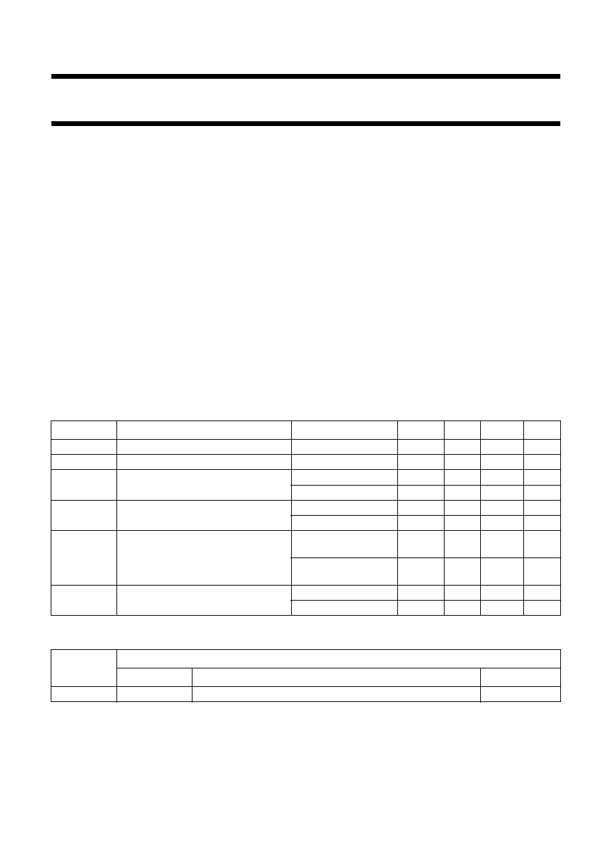
QUICK REFERENCE DATA
ORDERING INFORMATION
SYMBOL
PARAMETER
CONDITIONS
MIN.
TYP.
MAX.
UNIT
V
P
supply voltage
-
5.0
-
V
I
P
supply current
-
50
-
mA
f
R
frequency range
band A
55.25
-
361.25
MHz
band C
367.25
-
801.25
MHz
N
noise figure
band A
-
9.5
-
dB
band C
-
10
-
dB
V
o
IF output voltage
band A; R
L
= 75
;
1% cross modulation
-
108
-
dB
µ
V
band C; R
L
= 75
;
1% cross modulation
-
108
-
dBm
G
v
voltage gain
band A; R
L
= 75
-
19
-
dB
band C; R
L
= 75
-
29
-
dB
TYPE
NUMBER
PACKAGE
NAME
DESCRIPTION
VERSION
TDA5732M
SSOP20
plastic shrink small outline package; 20 leads; body width 4.4 mm
SOT266-1

1995 Mar 22
3
Philips Semiconductors
Preliminary specification
Low power VHF, UHF mixer/oscillator
for TV and VCR 2-band tuners
TDA5732M
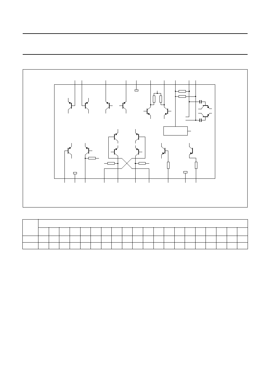
BLOCK DIAGRAM
Fig.1 Block diagram.
handbook, full pagewidth
MBE391
BAND C
OSCILLATOR
4
5
6
7
BAND A
OSCILLATOR
1
3
2
GND
band A oscillator
tuned circuit
band C oscillator
tuned circuit
MIXER
MIXER
BAND A
STAGE
BAND C
STAGE
LOCAL
OSCILLATOR
AMPLIFIER
ELECTRONIC
BAND SWITCH
8
band switch
input
DC
STABILIZER
IF
AMPLIFIER
10
IF output
IF ground
15
14
13
12
11
18
17
16
RFGND
band C input
20
19
band A input
local oscillator
amplifier outputs
V
P
IF inputs
TDA5732M
1995 Mar 22
4
Philips Semiconductors
Preliminary specification
Low power VHF, UHF mixer/oscillator
for TV and VCR 2-band tuners
TDA5732M
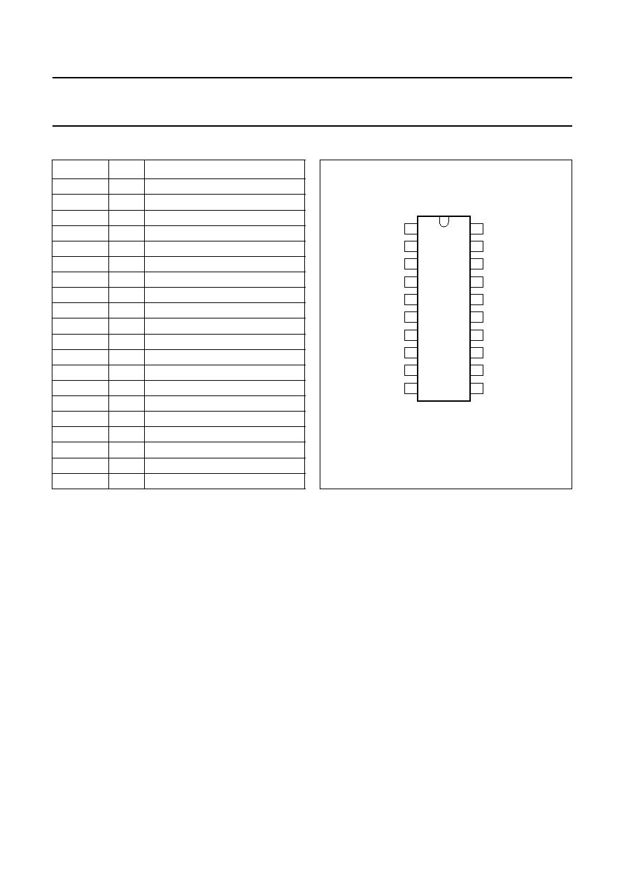
PINNING
SYMBOL
PIN
DESCRIPTION
AOSCIB
1
band A oscillator input base
GND
2
ground (0 V)
AOSCOC
3
band A oscillator output collector
COSCIB1
4
band C oscillator input base 1
COSCOC1
5
band C oscillator output collector 1
COSCOC2
6
band C oscillator output collector 2
COSCIB2
7
band C oscillator input base 2
BS
8
electronic band switch input
IFGND
9
ground for IF inputs
IFOUT
10
IF amplifier output
IFIN1
11
IF amplifier input 1
IFIN2
12
IF amplifier input 2
V
P
13
supply voltage
LOOUT1
14
local oscillator amplifier output 1
LOOUT2
15
local oscillator amplifier output 2
RFGND
16
ground for RF inputs
CIN1
17
band C input 1
CIN2
18
band C input 2
AIN1
19
band A input 1
AIN2
20
band A input 2
Fig.2 Pin configuration.
handbook, halfpage
TDA5732M
MBE390
1
2
3
4
5
6
7
8
9
10
20
19
18
17
16
15
14
13
12
11
BS
V
IFOUT
IFIN1
IFGND
IFIN2
COSCIB2
LOOUT1
COSCOC2
LOOUT2
COSCOC1
RFGND
COSCIB1
CIN1
AOSCOC
CIN2
GND
AIN1
AOSCIB
AIN2
P

1995 Mar 22
5
Philips Semiconductors
Preliminary specification
Low power VHF, UHF mixer/oscillator
for TV and VCR 2-band tuners
TDA5732M
LIMITING VALUES
In accordance with the Absolute Maximum Rating System (IEC 134).
THERMAL CHARACTERISTICS
HANDLING
Human body model: the IC withstands 2000 V (except pins 17 and 18 which withstand 1000 V) in accordance with
UZW-BO-FQ-A302; R = 1.5 k
; C = 100 pF.
Machine model: the IC withstands 200 V in accordance with
UZW-BO-FQ-B302; R = 0
; C = 200 pF.
SYMBOL
PARAMETER
MIN.
MAX.
UNIT
V
P
supply voltage range
-
0.3
+7.0
V
V
P(op)
operating supply voltage
4.5
5.5
V
V
n(max)
maximum voltage on each pin with a 22 k
resistor connected in
series
-
35
V
V
SW
switching voltage
0
7.0
V
T
stg
storage temperature
-
55
+150
∞
C
T
amb
operating ambient temperature
-
20
+85
∞
C
T
j
junction temperature
-
+150
∞
C
SYMBOL
PARAMETER
VALUE
UNIT
R
th j-a
thermal resistance from junction to ambient in free air
120
K/W
1995 Mar 22
6
Philips Semiconductors
Preliminary specification
Low power VHF, UHF mixer/oscillator
for TV and VCR 2-band tuners
TDA5732M
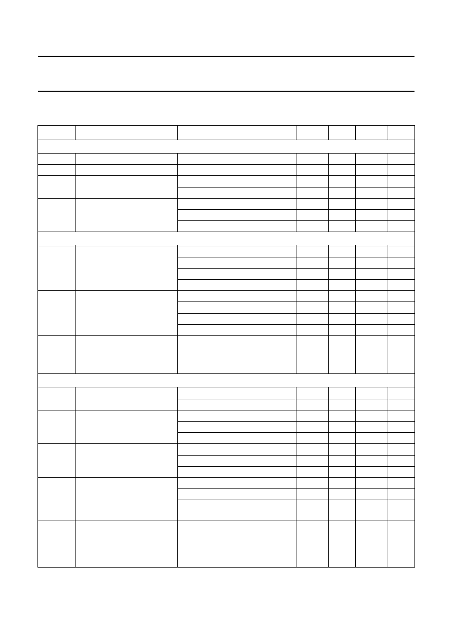
CHARACTERISTICS
V
P
= 5 V; T
amb
= 25
∞
C; unless otherwise specified.
SYMBOL
PARAMETER
CONDITIONS
MIN.
TYP.
MAX.
UNIT
Supply
V
P
supply voltage
4.5
5.0
5.5
V
I
P
supply current
I
P(max)
measured at V
P(max)
-
50
64
mA
V
SW
switching voltage
band A
0
-
2.0
V
band C
3.0
-
V
P
V
I
SW
switching current
band A; V
SW
= 0 V
-
-
2
µ
A
band C; V
SW
= 5 V
-
4.5
10
µ
A
V
P(max)
-
6
-
µ
A
IF amplifier
S
22
output reflection coefficient
f
i
= 43.5 MHz; see Fig.12
-
-
13.1
-
dB
f
i
= 43.5 MHz; see Fig.12
-
2.9
-
deg
f
i
= 58.75 MHz; see Fig.12
-
-
13.1
-
dB
f
i
= 58.75 MHz; see Fig.12
-
2.2
-
deg
Z
O
output impedance
f
i
= 43.5 MHz; see Fig.12
-
78.4
-
f
i
= 43.5 MHz; see Fig.12
-
1.8
-
f
i
= 58.75 MHz; see Fig.12
-
78.4
-
f
i
= 58.75 MHz; see Fig.12
-
-
1.4
-
SLO
visibility of the LO frequency at
the IF output
(worst case in the frequency
range of band A and band C)
R
L
= 75
-
85
-
dB
µ
V
Band A mixer (including IF amplifier)
f
R
frequency range
VHFl
55.25
-
127.25
MHz
VHFlll
133.25
-
361.25
MHz
N
A
noise figure
f
i
= 50 MHz; see Fig.7
-
8.5
9.5
dB
f
i
= 150 MHz; see Fig.7
-
8.5
10.5
dB
f
i
= 300 MHz; see Fig.7
-
9.5
12.5
dB
g
os
optimum source conductance
f
i
= 50 MHz; see Fig.7
-
0.7
-
mS
f
i
= 150 MHz; see Fig.7
-
0.9
-
mS
f
i
= 300 MHz; see Fig.7
-
1.5
-
mS
Y
I
input admittance (G
P
//C
P
)
G
P
; f
i
= 55.25 MHz; see Fig.9
-
0.25
-
mS
G
P
; f
i
= 361.25 MHz; see Fig.9
-
0.5
-
mS
C
P
; f
i
= 55.25 to 361.25 MHz;
see Fig.9
-
1.3
-
pF
V
oA(IF)
IF output voltage
1% cross modulation; in channel;
f
i
= 55.25 to 361.25 MHz;
R
L
= 75
; wanted frequency
sound carrier; unwanted frequency
picture carrier; see Fig.5
105
108
-
dB
µ
V

1995 Mar 22
7
Philips Semiconductors
Preliminary specification
Low power VHF, UHF mixer/oscillator
for TV and VCR 2-band tuners
TDA5732M
V
i(RF)
RF input voltage
f
i
= 173 MHz; note 1
-
91
-
dB
µ
V
f
i
= 407 MHz; note 1
-
83
-
dB
µ
V
G
v(A)
voltage gain at the channel
centre
f
IF
= 43.5 MHz; R
L
= 75
;
see Fig.3
16.5
19
21.5
dB
Band A oscillator
f
R
frequency range
VHFl
101
-
173
MHz
VHFlll
179
-
407
MHz
f
shift
frequency shift (worst case in
the frequency range)
V
P
= 5%; note 2
-
44
100
kHz
V
P
= 10%; note 2
-
220
-
kHz
ripple(p-p)
ripple susceptibility of the
supply voltage
(peak-to-peak value
V
P
= 4.75 to 5.25 V; f
i
= 101 MHz;
note 3
-
78
-
mV
V
P
= 4.75 to 5.25 V; f
i
= 173 MHz;
note 3
-
34
-
mV
V
P
= 4.75 to 5.25 V; f
i
= 179 MHz;
note 3
-
8.0
-
mV
V
P
= 4.75 to 5.25 V; f
i
= 407 MHz;
note 3
-
10
-
mV
f
drift
frequency drift (worst case in
the frequency range)
T = 25
∞
C with no compensation;
NP0 capacitors; note 4
-
1800
2200
kHz
5 s to 15 min after switch on; note 5
-
630
1100
kHz
N
phase noise, carrier-to-noise
sideband (worst case in the
frequency range)
±
50 kHz; frequency offset;
B = 3 kHz
-
60
-
dBc
Band C mixer (including IF amplifier)
f
R
frequency range, picture
carrier
367.25
-
801.25
MHz
N
C
noise figure
(not corrected for image)
f
i
= 367.25 MHz
-
9
11
dB
f
i
= 801.25 MHz
-
10
12
dB
Z
I
input impedance (R
s
+ L
s
)
R
s
; f
i
= 367.25 MHz; see Fig.10
-
30
-
L
s
; f
i
= 367.25 MHz; see Fig.10
-
9
-
nH
R
s
; f
i
= 801.25 MHz; see Fig.10
-
38
-
L
s
; f
i
= 801.25 MHz; see Fig.10
-
6
-
nH
V
oC(IF)
IF output voltage
1% cross modulation; in channel;
f
i
= 365.25 to 801.25 MHz;
R
L
= 75
; wanted frequency
sound carrier; unwanted frequency
picture carrier; see Fig.6
105
108
-
dB
µ
V
V
i(RF)
RF input voltage
f
i
= 847 MHz; note 1
-
66
-
dB
µ
V
G
v(C)
voltage gain
f
IF
= 43.5 MHz; R
L
= 75
;
see Fig.4
26
29
32
dB
SYMBOL
PARAMETER
CONDITIONS
MIN.
TYP.
MAX.
UNIT

1995 Mar 22
8
Philips Semiconductors
Preliminary specification
Low power VHF, UHF mixer/oscillator
for TV and VCR 2-band tuners
TDA5732M
Notes
1. The RF signal is modulated with 50% AM at 15 kHz: The level of the RF signal is increased until there is a 23 dB
difference between the LO carrier and the sideband components.
2. The frequency shift is defined as a variation in oscillator frequency when the supply voltage varies from
V
P
= 5 to 4.75 V or from V
P
= 5 to 5.75 V.
3. The ripple susceptibility is measured for a 500 kHz ripple at the LO output with the set-up as illustrated in Fig.8. The
level of the ripple signal is increased until there is a 53.5 dB difference between the LO carrier and the sideband
components.
4. The frequency shift is defined as a variation in oscillator frequency when the supply voltage varies from
T
amb
= 25
∞
C to 0
∞
C or from T
amb
= 25
∞
C to 50
∞
C.
5. The switching on drift is defined as the variation in oscillator frequency between 5 seconds and 15 minutes after
switching on.
6. SRF: spurious signal on LO with respect to LO output signal;
a) RF voltage level = 1 V at f
i
= 55.25 to 225 MHz.
b) RF level = 2.5 dBm at f
i
= 225 to 361.25 MHz.
c) RF level =
-
10 dBm at f
i
= 367.25 to 801.25 MHz.
Band C oscillator
f
R
frequency range
413
-
847
MHz
f
shift
frequency shift
V
P
= 5%; note 2
-
46
200
kHz
V
P
= 10%; note 2
-
200
-
kHz
ripple(p-p)
ripple susceptibility of the
supply voltage
(peak-to-peak value
V
P
= 4.75 to 5.25 V; f
i
= 413 MHz
-
203
-
mV
V
P
= 4.75 to 5.25 V; f
i
= 847 MHz;
note 3
-
22
-
mV
f
drift
frequency drift (worst case in
the frequency range)
T = 25
∞
C with compensation;
note 4
-
1100
2500
kHz
5 s to 15 min after switching on;
note 5
-
300
1300
kHz
N
phase noise, carrier-to-noise
sideband (worst case in the
frequency range)
±
50 kHz; frequency offset;
B = 3 kHz
-
64
-
dBc
LO output
Y
O
output admittance (G
P
//C
P
)
G
P
; f
i
= 101 MHz; see Fig.11
-
2.4
-
mS
G
P
; f
i
= 847 MHz; see Fig.11
-
3.1
-
mS
C
P
; f
i
= 101 to 847 MHz; see Fig.11
-
0.5
-
pF
V
O
output voltage
R
L
= 50
; V
P
= 4.5 to 5.5 V;
V
t
= 0 to 28 V
83
90
100
dB
µ
V
SRF
spurious signal on LO output
with respect to LO output
signal
R
L
= 50
; note 6
-
-
15
-
10
dB
HLO
LO signal harmonics w.r.t. LO
signal
R
L
= 50
-
-
10.5
-
9.5
dB
SYMBOL
PARAMETER
CONDITIONS
MIN.
TYP.
MAX.
UNIT

1995 Mar 22
9
Philips Semiconductors
Preliminary specification
Low power VHF, UHF mixer/oscillator
for TV and VCR 2-band tuners
TDA5732M
Fig.3 Band A gain measurement.
Z
i
>> 50
V
i
= 2V
meas
(V
i
= 80 dB
µ
V); V
o
= V'
meas
◊
(50 + 25)/50; voltage gain for band A = 20log(V
o
/V
i
).
handbook, full pagewidth
MBE290
signal
source
V
V
D.U.T.
A IN
A IN
IF
out
e
50
25
50
50
V
out
in
V
meas
meas
V'
RMS
voltmeter
spectrum
analyzer
Fig.4 Band C gain measurement.
V
i
= V
meas
(V
i
= 70 dB
µ
V); V
o
= V'
meas
◊
(50 + 25)/50; voltage gain for band C = 20log(V
o
/V
i
).
handbook, full pagewidth
MBE289
signal
source
V
V
HYBRID
A
C
B
D
D.U.T.
C IN
C IN
e
50
25
50
50
50
out
V
meas
meas
V'
RMS
voltmeter
spectrum
analyzer
IF
out

1995 Mar 22
10
Philips Semiconductors
Preliminary specification
Low power VHF, UHF mixer/oscillator
for TV and VCR 2-band tuners
TDA5732M
Fig.5 Band A 1% cross modulation.
Wanted input signal = 80 dB
µ
V; Zi >> 50
wanted input signal = 2V
meas
; unwanted input signal modulated with 30% AM;
V
oA(IF)
= unwanted output signalV
o
when the output wanted signal is modulated with 0.3% AM.
handbook, full pagewidth
MBE288
wanted
input signal
source
V
HYBRID
A
C
B
D
D.U.T.
A IN
IF
out
A IN
ew
50
25
50
unwanted
input signal
source
50
50
eu
50
out
V
meas
V
modulation analyzer
(unwanted AM on
the output wanted
frequency)
wanted
input
signal
RMS
voltmeter
Fig.6 Band C 1% cross modulation.
Wanted input signal = 70 dB
µ
V; unwanted input signal modulated with 30% AM; V
oA(IF)
= unwanted output signal V
o
when the
output wanted signal is modulated with 0.3% AM.
handbook, full pagewidth
MBE287
wanted
input signal
source
V
HYBRID
A
C
B
D
HYBRID
A
C
B
D
D.U.T.
C IN
IF
out
C IN
ew
50
25
50
50
unwanted
input signal
source
50
50
eu
50
out
V
modulation analyzer
(unwanted AM on
the output wanted
frequency)
wanted
input
signal
RMS
voltmeter

1995 Mar 22
11
Philips Semiconductors
Preliminary specification
Low power VHF, UHF mixer/oscillator
for TV and VCR 2-band tuners
TDA5732M
Fig.7 Input circuit for minimum noise figure.
(a) For f
R
= 50 MHz:
mixer A frequency response measured = 57 MHz, loss = 0 dB
image suppression = 16 dB
C1 = 9 pF
C2 = 15 pF
L1 = 7 turns ( 5.5mm, wire diam. = 0.5 mm)
l1 = rigid cable (RIM): 5 cm long
(rigid cable (RIM); 33 dB/100 m; 50
,
96 pF/m).
handbook, full pagewidth
MBE286 - 1
L1
C2
C1
PCB
plug
plug
BNC
BNC
RIM-RIM
I1
C4
C3
PCB
RIM-RIM
I3
I2
(a)
(b)
(b) For f
R
= 180 MHz:
mixer A frequency response measured = 150.3 MHz, loss = 1.3 dB
image suppression = 13 dB
C3 = 5 pF
C4 = 25 pF
l2 = rigid cable (RIM): 30 cm long
l3 = rigid cable (RIM): 5 cm long
(rigid cable (RIM); 33 dB/100 m; 50
;
96 pF/m).
Fig.8 Measurement set-up for ripple measurement,
handbook, full pagewidth
MBE376
MEASUREMENT
TEST CIRCUIT
OF FIG. 14
f o
500 kHz
500 kHz
to
spectrum
analyser
ripple
signal
47
100
µ
F
100
µ
F
6.8 k
DC supply
V
P

1995 Mar 22
12
Philips Semiconductors
Preliminary specification
Low power VHF, UHF mixer/oscillator
for TV and VCR 2-band tuners
TDA5732M
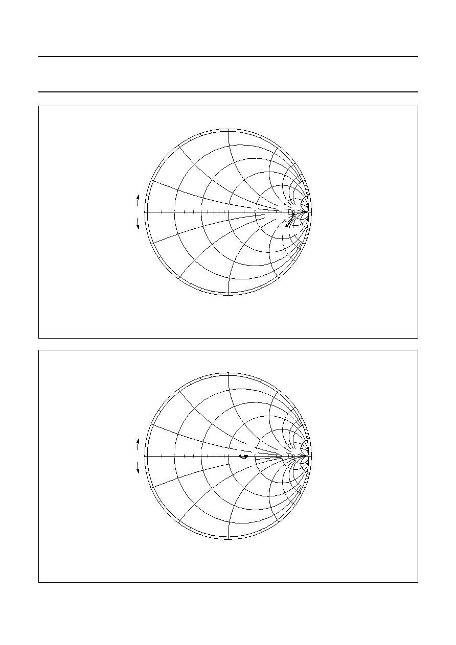
Fig.9 S
11
on VHF mixer input (Z chart; Z
o
= 50
).
handbook, full pagewidth
0.2
0.5
1
2
5
10
0.2
0.5
1
2
5
10
0
+ j
≠ j
MKA987
0.5
1
0.2
5
2
50 MHz
370 MHz
Fig.10 S
11
on UHF mixer input (Z chart; Z
o
= 50
).
handbook, full pagewidth
0.2
0.5
1
2
5
10
0.2
0.5
1
2
5
10
0
+ j
≠ j
MKA986
0.5
1
0.2
10
5
2
810 MHz
350 MHz
1995 Mar 22
13
Philips Semiconductors
Preliminary specification
Low power VHF, UHF mixer/oscillator
for TV and VCR 2-band tuners
TDA5732M
Fig.11 S
22
on LO output (Z chart; Z
o
= 50
).
handbook, full pagewidth
0.2
0.5
1
2
5
10
0.2
0.5
1
2
5
10
0
+ j
≠ j
MKA985
0.5
1
0.2
10
5
2
100 MHz
850 MHz
Fig.12 S
22
on IFoutput (Z chart; Z
o
= 50
).
handbook, full pagewidth
0.2
0.5
1
2
5
10
0.2
0.5
1
2
5
10
0
+ j
≠ j
MKA984
0.5
1
0.2
10
5
2
5 MHz
250 MHz
1995 Mar 22
14
Philips Semiconductors
Preliminary specification
Low power VHF, UHF mixer/oscillator
for TV and VCR 2-band tuners
TDA5732M
INTERNAL PIN CONFIGURATION
Table 1
Average DC voltage on pins
UHF/
VHF
PINS
1
2
3
4
5
6
7
8
9
10
11
12
13
14
15
16
17
18
19
20
VHF
1.8
0
3
-
3.6
3.6
-
0
0
2.1
3.6
3.6
5
4.2
4.2
0
-
-
1.8
1.8
UHF
-
0
3.6
1.9
2.9
2.9
1.9
5
0
2.1
3.6
3.6
5
4.2
4.2
0
1
1
-
-
Fig.13 Internal pin configuration.
handbook, full pagewidth
1
2
3
4
5
6
7
MBE393
10
13
12
11
18
17
16
20
19
8
9
TDA5732M
Vs
Vs
Vs
Vs
Vs
ground
BAND A OSCILLATOR
BAND C OSCILLATOR
BAND SWITCH
IF OUTPUT
STABILIZER
15
14
Vp
LO OUTPUT
IF FILTER
BAND C INPUT
BAND A INPUT
RF ground
IF ground

1995 Mar 22
15
Philips Semiconductors
Preliminary specification
Low power VHF, UHF mixer/oscillator
for TV and VCR 2-band tuners
TDA5732M
APPLICATION INFORMATION
Fig.14 Measurement test circuit.
handbook, full pagewidth
C6
1
2
3
C7
C11
4
C12
5
C9
C13
6
C14
7
R8
D3
L3
C10
C3
L4
R9
MBE392
BAND C
OSCILLATOR
BAND A
OSCILLATOR
MIXER
MIXER
BAND A
STAGE
BAND C
STAGE
LOCAL
OSCILLATOR
AMPLIFIER
ELECTRONIC
BAND SWITCH
DC
STABILIZER
IF
AMPLIFIER
10
15
14
13
12
11
18
17
16
20
19
8
C29
A
C
5 V
9
C17
R14 IF out
50
NETWORK
MEASUREMENT
50
NETWORK
MEASUREMENT
C2
R2
R3
C1
R1
D1
5 V
L1
L2
C4
R4
C5
D2
R6
R7
R5
C28
C30
C8
V
C24
C26
C27
C23
C22
R10
ANZAC-183-4
HYBRID
C21
C20
ANZAC-183-4
HYBRID
C19
C18
50
50
50
50
5 V
L7
TDA5732M
t
1995 Mar 22
16
Philips Semiconductors
Preliminary specification
Low power VHF, UHF mixer/oscillator
for TV and VCR 2-band tuners
TDA5732M
Application diagram components values
Table 2
Capacitors (all SMD and NP0 except
C9 to C11 to C14 and C29)
NUMBER
VALUE
C1
1 nF
C2
1 nF
C3
1 nF
C4
82 pF
C5
2.2 nF
C6
2.2 nF
C7
1.5 pF
C8
2.2 nF
C9
6 pF (N750)
C10
100 pF
C11
1 pF (N1500)
C12
2 pF (N750)
C13
2 pF (N750)
C14
1 pF (N1500)
C17
1 nF
C18
1 nF
C19
1 nF
C20
1 nF
C21
1 nF
C22
1 nF
C23
1 nF
C24
1 nF
C26
15 pF
C27
15 pF
C28
2.2 nF
C29
1 nF
C30
1
µ
F (40 V electrolytic
capacitor)
Table 3
Resistors (all SMD)
Table 4
Diodes and coils
Note
1. Wire size for L1 to L4 is 0.4 mm
Transformer (L7 = 2 turns)
Coil type: TOKO 7kN; material: 113kN, screw core
(03-0093), pot core (04-0026).
NUMBER
VALUE
R1
10
R2
12 k
R3
2.7 k
R4
47 k
R5
10
R6
47 k
R7
22 k
R8
2.2 k
R9
22 k
R10
100
R14
27
NUMBER
VALUE
Diodes
D1
BA792
D2
BB133
D3
BB134
Coils
(1)
L1
6 t (3.5 mm)
L2
3 t (2.5 mm)
L3
2 t (2.5 mm)
L4
3 t (3 mm)
1995 Mar 22
17
Philips Semiconductors
Preliminary specification
Low power VHF, UHF mixer/oscillator
for TV and VCR 2-band tuners
TDA5732M
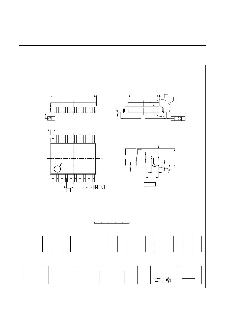
PACKAGE OUTLINE
UNIT
A
1
A
2
A
3
b
p
c
D
(1)
E
(1)
(1)
e
H
E
L
L
p
Q
Z
y
w
v
REFERENCES
OUTLINE
VERSION
EUROPEAN
PROJECTION
ISSUE DATE
IEC
JEDEC
EIAJ
mm
0.15
0
1.4
1.2
0.32
0.20
0.20
0.13
6.6
6.4
4.5
4.3
0.65
1.0
0.2
6.6
6.2
0.65
0.45
0.48
0.18
10
0
o
o
0.13
0.1
DIMENSIONS (mm are the original dimensions)
Note
1. Plastic or metal protrusions of 0.20 mm maximum per side are not included.
0.75
0.45
SOT266-1
90-04-05
95-02-25
w
M
A
A
1
A
2
b
p
D
H
E
L
p
Q
detail X
E
Z
e
c
L
v
M
A
X
(A )
3
A
y
0.25
1
10
20
11
pin 1 index
0
2.5
5 mm
scale
SSOP20: plastic shrink small outline package; 20 leads; body width 4.4 mm
SOT266-1
A
max.
1.5

1995 Mar 22
18
Philips Semiconductors
Preliminary specification
Low power VHF, UHF mixer/oscillator
for TV and VCR 2-band tuners
TDA5732M
SOLDERING
Plastic small outline packages
B
Y WAVE
During placement and before soldering, the component
must be fixed with a droplet of adhesive. After curing the
adhesive, the component can be soldered. The adhesive
can be applied by screen printing, pin transfer or syringe
dispensing.
Maximum permissible solder temperature is 260
∞
C, and
maximum duration of package immersion in solder bath is
10 s, if allowed to cool to less than 150
∞
C within 6 s.
Typical dwell time is 4 s at 250
∞
C.
A modified wave soldering technique is recommended
using two solder waves (dual-wave), in which a turbulent
wave with high upward pressure is followed by a smooth
laminar wave. Using a mildly-activated flux eliminates the
need for removal of corrosive residues in most
applications.
B
Y SOLDER PASTE REFLOW
Reflow soldering requires the solder paste (a suspension
of fine solder particles, flux and binding agent) to be
applied to the substrate by screen printing, stencilling or
pressure-syringe dispensing before device placement.
Several techniques exist for reflowing; for example,
thermal conduction by heated belt, infrared, and
vapour-phase reflow. Dwell times vary between 50 and
300 s according to method. Typical reflow temperatures
range from 215 to 250
∞
C.
Preheating is necessary to dry the paste and evaporate
the binding agent. Preheating duration: 45 min at 45
∞
C.
R
EPAIRING SOLDERED JOINTS
(
BY HAND
-
HELD SOLDERING
IRON OR PULSE
-
HEATED SOLDER TOOL
)
Fix the component by first soldering two, diagonally
opposite, end pins. Apply the heating tool to the flat part of
the pin only. Contact time must be limited to 10 s at up to
300
∞
C. When using proper tools, all other pins can be
soldered in one operation within 2 to 5 s at between 270
and 320
∞
C. (Pulse-heated soldering is not recommended
for SO packages.)
For pulse-heated solder tool (resistance) soldering of VSO
packages, solder is applied to the substrate by dipping or
by an extra thick tin/lead plating before package
placement.
DEFINITIONS
LIFE SUPPORT APPLICATIONS
These products are not designed for use in life support appliances, devices, or systems where malfunction of these
products can reasonably be expected to result in personal injury. Philips customers using or selling these products for
use in such applications do so at their own risk and agree to fully indemnify Philips for any damages resulting from such
improper use or sale.
Data sheet status
Objective specification
This data sheet contains target or goal specifications for product development.
Preliminary specification
This data sheet contains preliminary data; supplementary data may be published later.
Product specification
This data sheet contains final product specifications.
Limiting values
Limiting values given are in accordance with the Absolute Maximum Rating System (IEC 134). Stress above one or
more of the limiting values may cause permanent damage to the device. These are stress ratings only and operation
of the device at these or at any other conditions above those given in the Characteristics sections of the specification
is not implied. Exposure to limiting values for extended periods may affect device reliability.
Application information
Where application information is given, it is advisory and does not form part of the specification.