 | –≠–ª–µ–∫—Ç—Ä–æ–Ω–Ω—ã–π –∫–æ–º–ø–æ–Ω–µ–Ω—Ç: TDA6120 | –°–∫–∞—á–∞—Ç—å:  PDF PDF  ZIP ZIP |

DATA SHEET
Preliminary specification
Supersedes data of 1997 Jul 17
File under Integrated Circuits, IC02
1997 Aug 27
INTEGRATED CIRCUITS
TDA6120Q
Video output amplifier

1997 Aug 27
2
Philips Semiconductors
Preliminary specification
Video output amplifier
TDA6120Q
FEATURES
∑
High large signal bandwidth of 32 MHz (typ.) at
125 V (p-p)
∑
High small signal bandwidth of 47 MHz (typ.) at
60 V (p-p)
∑
Rise/fall time of 12.5 ns for 125 V (p-p)
∑
High slew rate of 10 V/ns
∑
Low static power dissipation of 2.5 W at 200 V supply
voltage
∑
High maximum output voltage
∑
Bandwidth independent of voltage gain
∑
Maximum overall voltage gain over 46 dB
∑
High Power Supply Rejection Ratio (PSRR)
∑
Fast cathode current measurement output for dark
current control loop
∑
Differential voltage input.
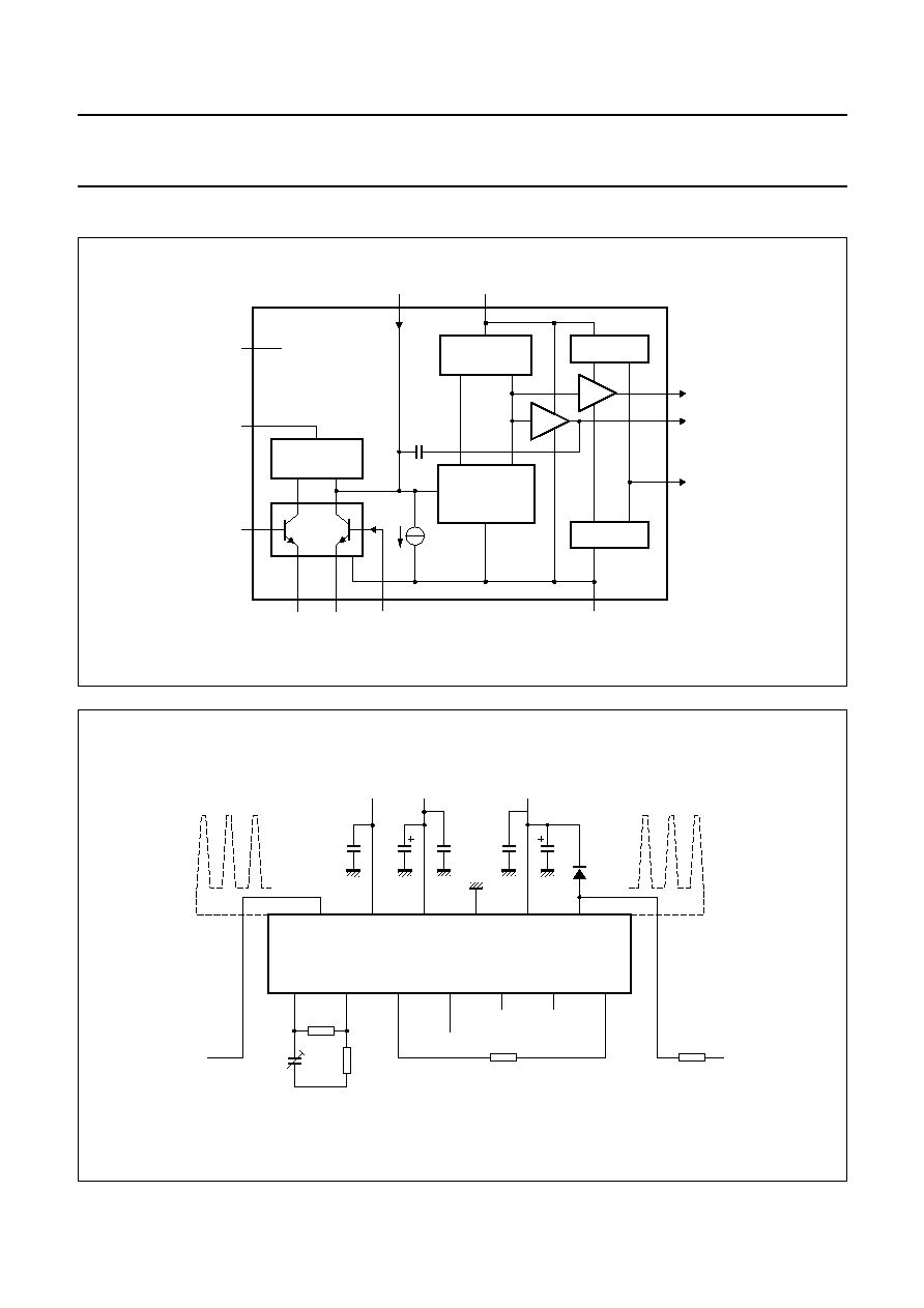
GENERAL DESCRIPTION
The TDA6120Q is a single 30 MHz, 125 V (p-p) video
output amplifier contained in a plastic DIL-bent-SIL power
package. The device uses high-voltage DMOS technology
and is intended to drive the cathodes of a CRT in High
Definition TVs (HDTVs) or monitors.
ORDERING INFORMATION
TYPE
NUMBER
PACKAGE
NAME
DESCRIPTION
VERSION
TDA6120Q
DBS13P
plastic DIL-bent-SIL power package; 13 leads (lead length 7.7 mm)
SOT141-8
1997 Aug 27
3
Philips Semiconductors
Preliminary specification
Video output amplifier
TDA6120Q
BLOCK DIAGRAM
Fig.1 Block diagram.
handbook, full pagewidth
MGK440
1
◊
1
◊
CURRENT
INPUT
out 1
◊
in
out 4
◊
MIRROR
1
◊
in
out
CASCODE
MIRROR
4
◊
in
out
CASCODE
+
J
5 mA
0.7 pF
TDA6120Q
9, 11
6
2
n.c.
VCC
VIN
-
1
3
4
RC
-
RC
+
VIN
+
8
GND
12
13
7
OUTC
OUT
OUTM
IIN
VDD
10
5
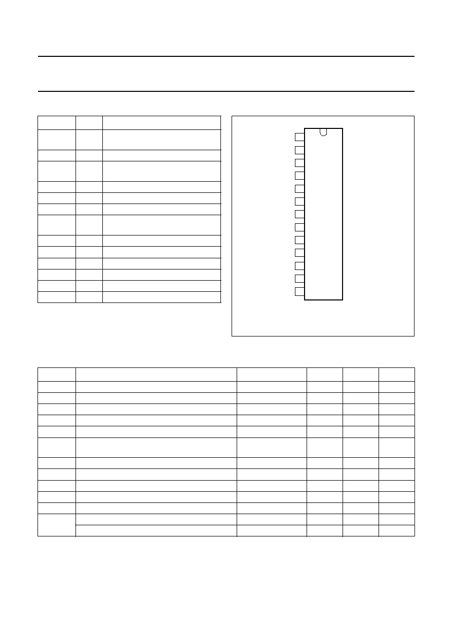
Fig.2 Top view.
handbook, full pagewidth
MGK441
442
68 pF
C1
RC
-
RC
+
1
3
5
7
9
11
13
2
4
6
8
10
12
22
VIN
-
VIN
+
Cr
10 nF
CCC
10
µ
F
CDD
3.3
µ
F
CC
22
nF
CD
22
nF
TDA6120Q
22 k
Rf
IIN
OUTM
n.c.
n.c.
OUT
CRT
VIN
147
Rflash
VCC
VDD
Dflash
OUTC
GND
+
12 V
+
200 V
Vref
Ria
Ri
1997 Aug 27
4
Philips Semiconductors
Preliminary specification
Video output amplifier
TDA6120Q
PINNING
SYMBOL
PIN
DESCRIPTION
RC
-
1
inverting input pre-emphasis
network
VIN
-
2
inverting voltage input
RC+
3
non-inverting input pre-emphasis
network
VIN+
4
non-inverting voltage input
IIN
5
feedback current input
V
CC
6
low supply voltage (12 V)
OUTM
7
cathode current measurement
output
GND
8
power ground and heatsink
n.c.
9
not connected
V
DD
10
high supply voltage (200 V)
n.c.
11
not connected
OUTC
12
cathode output
OUT
13
feedback output
Fig.3 Pin configuration.
handbook, halfpage
RC
-
VIN
-
RC
+
VIN
+
IIN
VCC
OUTM
GND
n.c.
VDD
n.c.
OUTC
OUT
1
2
3
4
5
6
7
8
9
10
11
12
13
TDA6120Q
MGK438
LIMITING VALUES
In accordance with the Absolute Maximum Rating System (IEC 134).
Note
1. 1250 V for IIN (pin 5).
SYMBOL
PARAMETER
CONDITIONS
MIN.
MAX.
UNIT
V
DD
high supply voltage
0
280
V
V
CC
low supply voltage
0
20
V
V
i
input voltage (pins 2 and 4)
0
V
CC
V
V
i(dif)
differential mode input voltage (pins 2 and 4)
-
V
CC
V
CC
V
V
i(pe)
pre-emphasis input voltage (pins 1 and 3)
0
V
CC
V
V
i(dif)(pe)
differential mode pre-emphasis input voltage
(pins 1 and 3)
-
V
CC
V
CC
V
V
IIN
input voltage (pin 5)
0
2V
BE
V
V
OUTM
measurement output voltage
0
20
V
V
o
output voltage (pins 12 and 13)
0
V
DD
V
T
stg
storage temperature
-
55
+150
∞
C
T
j
junction temperature
-
20
+150
∞
C
V
ESD
voltage peak human body model
note 1
-
2000
V
voltage peak machine model
-
300
V
1997 Aug 27
5
Philips Semiconductors
Preliminary specification
Video output amplifier
TDA6120Q
QUALITY SPECIFICATION
Quality specification in accordance with
"SNW-FQ-611 part E".
THERMAL CHARACTERISTICS
SYMBOL
PARAMETER
VALUE
UNIT
R
th j-c
thermal resistance from junction to case
3.0
K/W
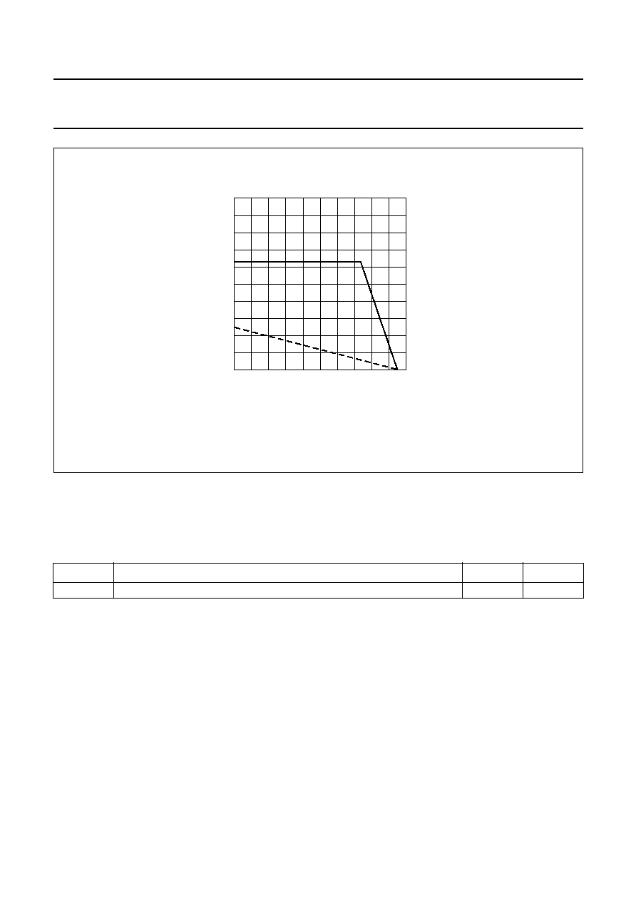
Fig.4 Power derating curve.
(1) Infinite heatsink.
(2) No heatsink.
handbook, halfpage
-
20
160
20
0
(1)
(2)
4
MGK442
8
12
16
0
40
20
80
120
Tamb (
∞
C)
Ptot
(W)