 | –≠–ª–µ–∫—Ç—Ä–æ–Ω–Ω—ã–π –∫–æ–º–ø–æ–Ω–µ–Ω—Ç: TDA6503TS | –°–∫–∞—á–∞—Ç—å:  PDF PDF  ZIP ZIP |
Document Outline
- CONTENTS
- 1 FEATURES
- 2 APPLICATIONS
- 3 GENERAL DESCRIPTION
- 3.1 I2C-bus format
- 3.2 3-wire bus format
- 4 QUICK REFERENCE DATA
- 5 ORDERING INFORMATION
- 6 BLOCK DIAGRAM
- 7 PINNING
- 8 FUNCTIONAL DESCRIPTION
- 8.1 Control mode selection
- 8.2 I2C-bus data format: pin SW to ground
- 8.3 3-wire bus data format: pin SW to VCC or open-circuit
- 9 LIMITING VALUES
- 10 THERMAL CHARACTERISTICS
- 11 CHARACTERISTICS
- 12 TIMING CHARACTERISTICS
- 13 TEST AND APPLICATION INFORMATION
- 13.1 Test circuits
- 13.2 Measurement circuit
- 13.3 Tuning amplifier
- 13.4 Crystal oscillator
- 13.5 Examples of I 2 C-bus data format sequences for TDA6502 and TDA6503
- 13.6 Examples of 3-wire bus data format sequences for TDA6502 and TDA6503
- 14 INTERNAL PIN CONFIGURATION
- 15 PACKAGE OUTLINE
- 16 SOLDERING
- 17 DATA SHEET STATUS
- 18 DEFINITIONS
- 19 DISCLAIMERS
- 20 PURCHASE OF PHILIPS I2C COMPONENTS

DATA SHEET
Product specification
Supersedes data of 2000 Aug 02
File under Integrated Circuits, IC02
2001 Aug 22
INTEGRATED CIRCUITS
TDA6502; TDA6502A; TDA6503;
TDA6503A
5 V mixers/oscillators and
synthesizers for cable TV and VCR
2-band tuners

2001 Aug 22
2
Philips Semiconductors
Product specification
5 V mixers/oscillators and synthesizers for
cable TV and VCR 2-band tuners
TDA6502; TDA6502A;
TDA6503; TDA6503A
CONTENTS
1
FEATURES
2
APPLICATIONS
3
GENERAL DESCRIPTION
3.1
I
2
C-bus format
3.2
3-wire bus format
4
QUICK REFERENCE DATA
5
ORDERING INFORMATION
6
BLOCK DIAGRAM
7
PINNING
8
FUNCTIONAL DESCRIPTION
8.1
Control mode selection
8.2
I
2
C-bus data format: pin SW to ground
8.2.1
I
2
C-bus address selection
8.2.2
Write mode
8.2.3
Read mode
8.2.4
Power-on reset
8.3
3-wire bus data format: pin SW to V
CC
or
open-circuit
8.3.1
Power-on reset
9
LIMITING VALUES
10
THERMAL CHARACTERISTICS
11
CHARACTERISTICS
12
TIMING CHARACTERISTICS
13
TEST AND APPLICATION INFORMATION
13.1
Test circuits
13.2
Measurement circuit
13.3
Tuning amplifier
13.4
Crystal oscillator
13.5
Examples of I
2
C-bus data format sequences for
TDA6502 and TDA6503
13.5.1
Write sequences to register C2
13.5.2
Read sequences from register C3
13.6
Examples of 3-wire bus data format sequences
for TDA6502 and TDA6503
13.6.1
18-bit sequence
13.6.2
19-bit sequence
13.6.3
27-bit sequence
14
INTERNAL PIN CONFIGURATION
15
PACKAGE OUTLINE
16
SOLDERING
16.1
Introduction to soldering surface mount
packages
16.2
Reflow soldering
16.3
Wave soldering
16.4
Manual soldering
16.5
Suitability of surface mount IC packages for
wave and reflow soldering methods
17
DATA SHEET STATUS
18
DEFINITIONS
19
DISCLAIMERS
20
PURCHASE OF PHILIPS I
2
C COMPONENTS

2001 Aug 22
3
Philips Semiconductors
Product specification
5 V mixers/oscillators and synthesizers for
cable TV and VCR 2-band tuners
TDA6502; TDA6502A;
TDA6503; TDA6503A
1
FEATURES
∑
Single-chip 5 V mixer/oscillator and synthesizer for
cable TV and VCR tuners
∑
Pin-to-pin compatible with TDA6402, TDA6402A,
TDA6403 and TDA6403A
∑
Universal bus protocol (I
2
C-bus or 3-wire bus):
≠ Bus protocol for 18 or 19-bit transmission (3-wire
bus)
≠ Extra protocol for 27-bit transmission (test modes and
features for 3-wire bus)
≠ Address + 4 data bytes transmission (I
2
C-bus `write'
mode)
≠ Address + 1 status byte (I
2
C-bus `read' mode)
≠ 4 independent I
2
C-bus addresses.
∑
1 PMOS buffer for UHF band selection (25 mA)
∑
3 PMOS buffers for general purpose, e.g. 2 VHF
sub-bands, FM sound trap (25 mA)
∑
33 V tuning voltage output
∑
In-lock detector
∑
5-step analog-to-digital converter (3 bits in I
2
C-bus
mode)
∑
15-bit programmable divider
∑
Programmable reference divider ratio (64, 80 or 128)
∑
Programmable charge pump current (60 or 280
µ
A)
∑
Varicap drive disable
∑
Balanced mixer with a common emitter input for VHF
(single input)
∑
Balanced mixer with a common base input for UHF
(balanced input)
∑
2-pin common emitter oscillator for VHF
∑
4-pin common emitter oscillator for UHF
∑
IF preamplifier with asymmetrical 75
output
impedance able to drive loads from 75
upwards
∑
Low power
∑
Low radiation
∑
Small size
∑
The TDA6502A and TDA6503A differ from the TDA6502
and TDA6503 by the UHF port protocol in the I
2
C-bus
mode (see Tables 3 and 4).
2
APPLICATIONS
∑
Cable tuners for TV and VCR (switched concept for
VHF).
3
GENERAL DESCRIPTION
The TDA6502, TDA6502A, TDA6503 and TDA6503A are
programmable 2-band mixers/oscillators and synthesizers
intended for VHF/UHF TV and VCR tuners (see Fig.1).
Partitioning of the bands is up to the customer as long as
VHF is below 500 MHz and UHF is below 900 MHz.
The devices include two double balanced mixers and two
oscillators for the VHF and UHF band respectively, an
IF amplifier and a PLL synthesizer. The VHF band can be
split-up into two sub-bands using a proper oscillator
application and a switchable inductor.
Two pins are available between the mixer output and the
IF amplifier input to enable IF filtering for improved signal
handling.
The port register provides four PMOS ports. Band
selection is provided by port register UHF. When port
register UHF is `on', the UHF mixer-oscillator is active and
the VHF band is switched off. When port register UHF is
`off', the VHF mixer-oscillator is active and the UHF band
is off. Port registers VHFL and VHFH are used to select
the VHF sub-bands. Port register FMST is a general
purpose port, that can be used to switch an FM sound trap.
When the ports are used, the sum of the drain currents has
to be limited to 30 mA.
The synthesizer consists of a 15-bit programmable divider,
a crystal oscillator and its programmable reference divider
and a phase comparator (phase/frequency detector)
combined with a charge pump which drives the tuning
amplifier, including the 33 V output at pin VT. Depending
on the reference divider ratio (64, 80 or 128), the phase
comparator operates at 62.5, 50 or 31.25 kHz with a
4 MHz crystal.

2001 Aug 22
4
Philips Semiconductors
Product specification
5 V mixers/oscillators and synthesizers for
cable TV and VCR 2-band tuners
TDA6502; TDA6502A;
TDA6503; TDA6503A
Depending on the voltage applied to pin SW (see Table 2)
the device is operating in the I
2
C-bus mode or 3-wire bus
mode.
In the 3-wire bus mode, pin LOCK/ADC is the `lock' output
of the PLL and is at LOW level when the PLL is locked.
Lock detector bit FL of the status byte is set to logic 1 when
the loop is locked and is read on the SDA line during a
READ operation in I
2
C-bus mode only.
In the I
2
C-bus mode only, pin LOCK/ADC is the ADC input
for digital AFC control. The ADC code is read during a
READ operation on the I
2
C-bus.
In the test mode, in both I
2
C-bus mode and 3-wire bus
mode, pin LOCK/ADC is used as a test output for f
REF
and
1
/
2
f
DIV
.
3.1
I
2
C-bus format
Five serial bytes (including the address byte) are required
to address the device, select the VCO frequency, program
the four ports, set the charge pump current and set the
reference divider ratio. The device has four independent
I
2
C-bus addresses which can be selected by applying a
specific voltage to pin CE/AS.
3.2
3-wire bus format
Data is transmitted to the device during a HIGH level on
pin CE/AS (enable line). The device is accessible with
18-bit and 19-bit data formats (see Figs 4 and 5). The first
four bits are used to program the PMOS ports and the
remaining bits control the programmable divider. A 27-bit
data format (see Fig.6) may also be used to set the charge
pump current, the reference divider ratio and the test
modes.
It is not allowed to address the device with words whose
length is different from 18, 19 or 27 bits.
Table 1
Data word length for 3-wire bus format
Note
1. The selection of the reference divider is given by an
automatic identification of the data word length. When
the 27-bit format is used, the reference divider is
controlled by bits RSA and RSB (see Table 8). More
details are given in Section 8.3.
DATA WORD
REFERENCE
DIVIDER
(1)
FREQUENCY
STEP
18-bit
64
62.50 kHz
19-bit
128
31.25 kHz
27-bit
programmable
programmable

2001 Aug 22
5
Philips Semiconductors
Product specification
5 V mixers/oscillators and synthesizers for
cable TV and VCR 2-band tuners
TDA6502; TDA6502A;
TDA6503; TDA6503A
4
QUICK REFERENCE DATA
Measured over full voltage and temperature ranges.
Notes
1. One buffer `on', I
o
= 25 mA; two buffers `on', maximum sum of I
o
= 30 mA.
2. The power dissipation is calculated as follows:
where:
V
P(sat)
= output saturation voltage on the buffer output
I
o
= source current for one buffer output.
5
ORDERING INFORMATION
SYMBOL
PARAMETER
CONDITIONS
MIN.
TYP.
MAX.
UNIT
V
CC
supply voltage
operating
4.5
5
5.5
V
I
CC
supply current
all PMOS ports are off;
V
CC
= 5V
-
71
-
mA
f
XTAL
crystal oscillator frequency
-
4.0
-
MHz
I
o(PMOS)
PMOS port output current
note 1
-
-
30
mA
P
tot
total power dissipation
note 2
-
-
520
mW
T
stg
IC storage temperature
-
40
-
+150
∞
C
T
amb
ambient temperature
-
20
-
+85
∞
C
f
RF
RF frequency
VHF band
40
-
800
MHz
UHF band
200
-
900
MHz
G
V
voltage gain
VHF band
-
20
-
dB
UHF band
-
32
-
dB
NF
noise figure
VHF band
-
7.5
-
dB
UHF band
-
7
-
dB
V
o
output voltage (causing 1% cross
modulation in channel)
VHF band
-
110
-
dB
µ
V
UHF band
-
110
-
dB
µ
V
TYPE
NUMBER
PACKAGE
NAME
DESCRIPTION
VERSION
TDA6502
SSOP28
plastic shrink small outline package; 28 leads; body width 5.3 mm
SOT341-1
TDA6502A
TDA6503
TDA6503A
P
tot
V
CC
I
CC
I
o
≠
(
)
V
P(sat)
I
o
0.5
33V
◊
(
)
2
22 k
---------------------------------
+
◊
+
◊
=

2001 Aug 22
6
Philips Semiconductors
Product specification
5 V mixers/oscillators and synthesizers for
cable TV and VCR 2-band tuners
TDA6502; TDA6502A;
TDA6503; TDA6503A
6
BLOCK DIAGRAM
handbook, full pagewidth
FCE527
REFERENCE
DIVIDER
64, 80, 128
XTAL
OSCILLATOR
4 MHz
15-BIT
PROGRAMMABLE
DIVIDER
15-BIT
FREQUENCY
REGISTER
POWER-DOWN
DETECTOR
PHASE
COMPARATOR
IN-LOCK
DETECTOR
CHARGE
PUMP
OPAMP
FL
T0, T1, T2
CP
OS
CP
T2
T1
T0 RSA RSB OS
CONTROL
REGISTER
FL
I
2
C-BUS / 3-WIRE BUS
TRANSCEIVER
3-BIT ADC
PORT
REGISTER
UHF
VHFH VHFL FMST
FL
fREF
fREF
1/2fDIV
fDIV
GATE
RF INPUT
VHF
VHF
MIXER
VHF
OSCILLATOR
RF INPUT
UHF
UHF
MIXER
UHF
OSCILLATOR
IF
PREAMPLIFIER
BS
BS
BS
BS
BS
BS
BS
T0, T1, T2
RSA
RSB
VHFIN
RFGND
UHFIN1
UHFIN2
XTAL
CL
DA
SW
CE/AS
IFFIL1 IFFIL2
VCC
VHFOSCOC
VHFOSCIB
OSCGND
IFOUT
UHFOSCIB2
UHFOSCOC2
UHFOSCOC1
UHFOSCIB1
CP
VT
GND
FMST
PVHFL
PVHFH
PUHF
LOCK/ADC
3 (26)
4 (25)
1 (28)
2 (27)
18 (11)
14 (15)
13 (16)
11 (18)
12 (17)
15 (14)
9 (20)
8 (21)
7 (22)
10 (19)
(8) 21
(12) 17
(13) 16
(4) 25
(3) 26
(2) 27
(1) 28
(9) 20
(6) 23
(7) 22
(5) 24
19 (10)
6 (23)
5 (24)
SCL
SDA
SW
CE/AS
TDA6502
TDA6502A
(TDA6503)
(TDA6503A)
Fig.1 Block diagram.
The pin numbers in parenthesis refer to the TDA6503 and TDA6503A.

2001 Aug 22
7
Philips Semiconductors
Product specification
5 V mixers/oscillators and synthesizers for
cable TV and VCR 2-band tuners
TDA6502; TDA6502A;
TDA6503; TDA6503A
7
PINNING
SYMBOL
PIN
DESCRIPTION
TDA6502;
TDA6502A
TDA6503;
TDA6503A
UHFIN1
1
28
UHF RF input 1
UHFIN2
2
27
UHF RF input 2
VHFIN
3
26
VHF RF input
RFGND
4
25
RF ground
IFFIL1
5
24
IF filter output 1
IFFIL2
6
23
IF filter output 2
PVHFL
7
22
PMOS port output, general purpose (e.g. VHF low sub-band)
PVHFH
8
21
PMOS port output, general purpose (e.g. VHF high sub-band)
PUHF
9
20
PMOS port output, UHF band
FMST
10
19
PMOS port output, general purpose (e.g. FM sound trap)
SW
11
18
bus format selection input: I
2
C-bus mode or 3-wire bus mode
CE/AS
12
17
chip enable input in 3-wire bus mode or address selection input in
I
2
C-bus mode
DA
13
16
serial data input/output
CL
14
15
serial clock input
LOCK/ADC
15
14
lock detector output in 3-wire bus mode or ADC input in I
2
C-bus
mode
CP
16
13
charge pump output
VT
17
12
tuning voltage output
XTAL
18
11
crystal oscillator input
V
CC
19
10
supply voltage
IFOUT
20
9
IF output
GND
21
8
digital ground
VHFOSCIB
22
7
VHF oscillator input base
OSCGND
23
6
oscillator ground
VHFOSCOC
24
5
VHF oscillator output collector
UHFOSCIB1
25
4
UHF oscillator input 1 (base)
UHFOSCOC1
26
3
UHF oscillator output 1 (collector)
UHFOSCOC2
27
2
UHF oscillator output 2 (collector)
UHFOSCIB2
28
1
UHF oscillator input 2 (base)

2001 Aug 22
8
Philips Semiconductors
Product specification
5 V mixers/oscillators and synthesizers for
cable TV and VCR 2-band tuners
TDA6502; TDA6502A;
TDA6503; TDA6503A
handbook, halfpage
UHFIN1
UHFIN2
VHFIN
RFGND
IFFIL1
IFFIL2
PVHFL
PVHFH
PUHF
FMST
SW
CE/AS
DA
CL
UHFOSCIB2
UHFOSCOC2
UHFOSCOC1
UHFOSCIB1
OSCGND
VHFOSCIB
VHFOSCOC
GND
IFOUT
VCC
XTAL
VT
CP
LOCK/ADC
1
2
3
4
5
6
7
8
9
10
11
12
13
28
27
26
25
24
23
22
21
20
19
18
17
16
15
14
TDA6502
TDA6502A
FCE570
Fig.2
Pin configuration for TDA6502 and
TDA6502A.
handbook, halfpage
UHFIN1
UHFIN2
VHFIN
RFGND
IFFIL1
IFFIL2
PVHFL
PVHFH
PUHF
FMST
SW
CE/AS
DA
CL
UHFOSCIB2
UHFOSCOC2
UHFOSCOC1
UHFOSCIB1
OSCGND
VHFOSCIB
VHFOSCOC
GND
IFOUT
VCC
XTAL
VT
CP
LOCK/ADC
1
2
3
4
5
6
7
8
9
10
11
12
13
28
27
26
25
24
23
22
21
20
19
18
17
16
15
14
TDA6503
TDA6503A
FCE571
Fig.3
Pin configuration for TDA6503 and
TDA6503A.
8
FUNCTIONAL DESCRIPTION
8.1
Control mode selection
The device is controlled via the I
2
C-bus or the 3-wire bus, depending on the voltage applied to pin SW (see Table 2).
A LOW level on pin SW enables the I
2
C-bus: pins CE/AS, DA and CL are used as address selection (AS), serial data
(SDA) and serial clock (SCL) input respectively.
A HIGH level on pin SW enables the 3-wire bus: pins CE/AS, DA and CL are used as chip enable (CE), data and clock
inputs respectively.
Table 2
Bus format selection
PIN
I
2
C-BUS MODE
3-WIRE BUS MODE
SYMBOL
TDA6502;
TDA6502A
TDA6503;
TDA6503A
SW
11
18
LOW-level voltage or ground
HIGH-level voltage or open-circuit
CE/AS
12
17
address selection input
enable input
DA
13
16
serial data input
data input
CL
14
15
serial clock input
clock input
LOCK/ADC
15
14
ADC input or test output
lock detector output or test output

2001 Aug 22
9
Philips Semiconductors
Product specification
5 V mixers/oscillators and synthesizers for
cable TV and VCR 2-band tuners
TDA6502; TDA6502A;
TDA6503; TDA6503A
8.2
I
2
C-bus data format: pin SW to ground
8.2.1
I
2
C-
BUS ADDRESS SELECTION
The module address contains programmable address
bits MA1 and MA0 (see Tables 3, 4 and 9) which offer the
possibility of having several synthesizers (up to 4) in one
system by applying a specific voltage on pin CE/AS.
The relationship between bits MA1 and MA0 and the input
voltage applied to pin CE/AS is given in Table 6.
8.2.2
W
RITE MODE
The write mode is defined by the address byte ADB with
bit R/W = 0 (see Tables 3 and 4).
Data bytes can be sent to the device after the address
transmission (first byte). Four data bytes are needed to
fully program the device.
The bus transceiver has an auto-increment facility which
permits the programming of the device within one single
transmission (address byte + 4 data bytes). The device
can also be partially programmed providing that the first
data byte following the address byte is divider byte DB1 or
the control byte CB.
The first bit of the byte following the address byte indicates
whether frequency data (first bit = 0) or control and
band-switch data (first bit = 1) will follow. Until an I
2
C-bus
STOP command is sent by the controller, additional data
bytes can be entered without the need to re-address the
device.
The frequency register is loaded after the 8th clock pulse
of byte DB2, the control register is loaded after the 8th
clock pulse of the byte CB and the band-switch register is
loaded after the 8th clock pulse of byte BB.
Table 3
I
2
C-bus data format for write mode of TDA6502 and TDA6503
Table 4
I
2
C-bus data format for write mode of TDA6502A and TDA6503A
NAME
BYTE
BIT
MSB
LSB
Address byte
ADB
1
1
0
0
0
MA1
MA0
R/W = 0
Divider byte 1
DB1
0
N14
N13
N12
N11
N10
N9
N8
Divider byte 2
DB2
N7
N6
N5
N4
N3
N2
N1
N0
Control byte
CB
1
CP
T2
T1
T0
RSA
RSB
OS
Band-switch byte
BB
X
X
X
X
FMST
PUHF
PVHFH
PVHFL
NAME
BYTE
BIT
MSB
LSB
Address byte
ADB
1
1
0
0
0
MA1
MA0
R/W = 0
Divider byte 1
DB1
0
N14
N13
N12
N11
N10
N9
N8
Divider byte 2
DB2
N7
N6
N5
N4
N3
N2
N1
N0
Control byte
CB
1
CP
T2
T1
T0
RSA
RSB
OS
Band-switch byte
BB
X
X
X
X
PUHF
FMST
PVHFH
PVHFL

2001 Aug 22
10
Philips Semiconductors
Product specification
5 V mixers/oscillators and synthesizers for
cable TV and VCR 2-band tuners
TDA6502; TDA6502A;
TDA6503; TDA6503A
Table 5
Description of the bits used in Tables 3 and 4
Table 6
Address selection bits (I
2
C-bus mode)
Table 7
Test mode bits
Notes
1. This is the default mode at Power-on reset.
2. The ADC input cannot be used when these test modes are active; see Section 8.2.3 for more information.
BIT
DESCRIPTION
MA1 and MA0
programmable address bits (see Table 6)
R/W
logic 0 for write mode
N14 to N0
programmable divider bits: N = N14
◊
2
14
+ N13
◊
2
13
+ ... + N1
◊
2
1
+ N0
CP
charge pump current control bit:
logic 0: charge pump current is 60
µ
A
logic 1: charge pump current is 280
µ
A (at power-on)
T2, T1 and T0
test bits (see Table 7)
RSA and RSB
reference divider ratio select bits (see Table 8)
OS
tuning amplifier control bit:
logic 0: tuning voltage is `on' (during normal operating)
logic 1: tuning voltage is `off'; high-impedance output of pin VT (at power-on)
PVHFL, PVHFH, PUHF and FMST
PMOS ports control bits:
logic 0: corresponding buffer is `off' (at power-on)
logic 1: corresponding buffer is `on'
X
don't care
MA1
MA0
VOLTAGE APPLIED TO PIN CE/AS
0
0
0 V to 0.1V
CC
0
1
0.2V
CC
to 0.3V
CC
or open-circuit
1
0
0.4V
CC
to 0.6V
CC
1
1
0.9V
CC
to 1.0V
CC
T2
T1
T0
TEST MODE
0
0
0
normal mode
0
0
1
normal mode (note 1)
0
1
X
charge pump is off
1
1
0
charge pump is sinking current
1
1
1
charge pump is sourcing current
1
0
0
f
REF
is available on pin LOCK/ADC (note 2)
1
0
1
1
/
2
f
DIV
is available on pin LOCK/ADC (note 2)

2001 Aug 22
11
Philips Semiconductors
Product specification
5 V mixers/oscillators and synthesizers for
cable TV and VCR 2-band tuners
TDA6502; TDA6502A;
TDA6503; TDA6503A
Table 8
Reference divider ratio select bits
8.2.3
R
EAD MODE
The read mode is defined by the address byte ADB with bit R/W = 1 (see Table 9).
After the slave address has been recognized, the device generates an acknowledge pulse and status byte SB is
transferred on the SDA line (MSB first). Data is valid on the SDA line during a HIGH level of the SCL line. A second data
byte can be read from the device if the microcontroller generates an acknowledge on the SDA line (master acknowledge).
End of transmission will occur if no master acknowledge occurs. The device will then release the data line to allow the
microcontroller to generate a STOP condition.
Bit POR is set to logic 1 at power-on. The bit is reset when an end-of-data is detected by the device (end of a read
sequence). Control of the loop is made possible with bit FL which indicates when the loop is locked (bit FL = 1)
A built-in ADC input is available on pin LOCK/ADC (I
2
C-bus mode only). This converter can be used to apply AFC
information to the microcontroller of the IF section of the television.
Table 9
Read data format
Note
1. MSB is transmitted first.
Table 10 Description of the bits used in Table 9
RSA
RSB
REFERENCE DIVIDER RATIO
FREQUENCY STEP (kHz)
X
0
80
50
0
1
128
31.25
1
1
64
62.5
NAME
BYTE
BIT
MSB
(1)
LSB
Address byte
ADB
1
1
0
0
0
MA1
MA0
R/W = 1
Status byte
SB
POR
FL
R
1
1
A2
A1
A0
BIT
DESCRIPTION
MA1 and MA0
programmable address bits (see Table 6)
R/W
logic 1 for read mode
POR
Power-on reset flag:
logic 0: after an end-of-data detected by the device
logic 1: at power-on
FL
in-lock flag:
logic 0: loop is not locked
logic 1: loop is locked
R
ready flag:
logic 0: mode after Power-on reset (bit T2 = 0, bit T1 = 0 and bit T0 = 1) and the PLL is locked
logic 1: in other conditions
A2, A1 and A0
digital output of the 5-level ADC (see Table 11)

2001 Aug 22
12
Philips Semiconductors
Product specification
5 V mixers/oscillators and synthesizers for
cable TV and VCR 2-band tuners
TDA6502; TDA6502A;
TDA6503; TDA6503A
Table 11 Output of ADC (note 1)
Note
1. Accuracy is
±
0.03
◊
V
CC
.
8.2.4
P
OWER
-
ON RESET
The power-on detection threshold voltage V
POR
is set to 3.2 V at room temperature. Below this threshold the device is
reset to the power-on state.
At power-on state the following actions take place:
∑
The charge pump current is set to 280
µ
A
∑
The tuning voltage output is disabled
∑
The test bits T2, T1 and T0 are set to logic `001'
∑
The divider bit RSB is set to logic 1
∑
Port register UHF is `off', which means that the UHF oscillator and the UHF mixer are switched off. Consequently, the
VHF oscillator and the VHF mixer are switched on. Port registers VHFL and VHFH are `off', which means that the VHF
tank circuit is operating in the VHF low sub-band. The tuning amplifier is switched off thus the tank circuit is supplied
with the maximum tuning voltage. The oscillator is therefore operating at the end of the VHF low sub-band.
Table 12 Default setting of the bits at Power-on reset
A2
A1
A0
VOLTAGE APPLIED TO PIN LOCK/ADC
0
0
0
0 to 0.15V
CC
0
0
1
0.15V
CC
to 0.30V
CC
0
1
0
0.30V
CC
to 0.45V
CC
0
1
1
0.45V
CC
to 0.60V
CC
1
0
0
0.60V
CC
to 1.00V
CC
NAME
BYTE
BIT
MSB
LSB
Address byte
ADB
1
1
0
0
0
MA1
MA0
X
Divider byte 1
DB1
0
X
X
X
X
X
X
X
Divider byte 2
DB2
X
X
X
X
X
X
X
X
Control byte
CB
1
1
0
0
1
X
1
1
Band switch byte
BB
X
X
X
X
0
0
0
0

2001 Aug 22
13
Philips Semiconductors
Product specification
5 V mixers/oscillators and synthesizers for
cable TV and VCR 2-band tuners
TDA6502; TDA6502A;
TDA6503; TDA6503A
8.3
3-wire bus data format: pin SW to V
CC
or
open-circuit
During a HIGH level on pin CE/AS (enable line), the data
is clocked into the data register at the HIGH-to-LOW
transition of the clock (see Figs 4, 5 and 6).
The first four bits control the PMOS ports and are loaded
into the internal band-switch register on the 5th rising edge
of the clock pulse.
The frequency bits are loaded into the frequency register
at the HIGH-to-LOW transition of the enable line when an
18-bit or 19-bit data word is transmitted. When a 27-bit
data word is transmitted, the frequency bits are loaded into
the frequency register on the 20th rising edge of the clock
pulse and the control bits at the HIGH-to-LOW transition of
the enable line (see Fig.6).
In this 27-bit data format mode the reference divider is
given by bits RSA and RSB (see Table 8).
The test bits T2, T1 and T0, the charge pump bit CP, the
ratio select bit RSB and bit OS can only be selected or
changed with a 27-bit transmission. They remain
programmed if an 18-bit or 19-bit transmission occurs.
Only bit RSA is controlled by the transmission length when
the 18-bit or 19-bit format is used. When an 18-bit data
word is transmitted, the most significant bit of the divider
(bit N14) is internally set to logic 0 and bit RSA is set to
logic 1. When a 19-bit data word is transmitted, bit RSA is
set to logic 0.
It is not allowed to address the devices with words whose
length is different from 18, 19 or 27 bits. A data word of
less than 18 bits will not affect the frequency register of the
device.
The definition of the bits is unchanged compared to the
I
2
C-bus mode.
8.3.1
P
OWER
-
ON RESET
The power-on detection threshold voltage V
POR
is set to
3.2 V at room temperature. Below this threshold the device
is reset to the power-on state.
At power-on state the following actions take place:
∑
The charge pump current is set to 280
µ
A
∑
The test bits T2, T1 and T0 are set to logic `001'
∑
The divider bit RSB is set to logic 1
∑
The tuning voltage output is disabled
∑
The tuning amplifier control bit OS is automatically reset
to logic 0 in 18-bit and 19-bit modes when the first data
word is received to allow normal operation
∑
Port register UHF is `off', which means that the UHF
oscillator and the UHF mixer are switched off.
Consequently, the VHF oscillator and the VHF mixer are
switched on. Port registers VHFL and VHFH are `off',
which means that the VHF tank circuit is operating in the
VHF low sub-band. The tuning amplifier is switched off
until the first transmission. In that case, the tank circuit
is supplied with the maximum tuning voltage.
The oscillator is therefore operating at the end of the
VHF low sub-band
∑
The reference divider ratio is set to 64 or 128 if the first
sequence to the device has 18 bits or 19 bits
respectively; if the sequence has 27 bits, the reference
divider ratio is set by bits RSA and RSB (see Table 8).

2001 Aug 22
14
Philips Semiconductors
Product specification
5 V mixers/oscillators and synthesizers for
cable TV and VCR 2-band tuners
TDA6502; TDA6502A;
TDA6503; TDA6503A
handbook, full pagewidth
FCE572
1
4
5
18
N13
N12 N11
N10
N9
N8
N7
N6
N5
N4
N3
N2
N1
N0
PUHF
FMST
PVHFH
PVHFL
INVALID
DATA
BAND-SWITCH
DATA
FREQUENCY
DATA
INVALID
DATA
LOAD BAND-SWITCH
REGISTER
LOAD FREQUENCY
REGISTER
DA
CL
CE
Fig.4 18-bit data format (bit RSA = 1).
handbook, full pagewidth
FCE573
1
4
5
19
N13
N14
N12 N11 N10
N9
N8
N7
N6
N5
N4
N3
N2
N1
N0
PUHF
FMST
PVHFH
PVHFL
INVALID
DATA
BAND-SWITCH
DATA
FREQUENCY
DATA
INVALID
DATA
LOAD BAND-SWITCH
REGISTER
LOAD FREQUENCY
REGISTER
DA
CL
CE
Fig.5 19-bit data format (bit RSA = 0).

2001 Aug 22
15
Philips Semiconductors
Product specification
5 V mixers/oscillators and synthesizers for
cable TV and VCR 2-band tuners
TDA6502; TDA6502A;
TDA6503; TDA6503A
FCE574
1
4
5
27
20
19
N13
N14
N12
N2
N1
N0
X
CP
T2
T1
T0 RSA RSB
OS
PUHF
FMST
PVHFH
PVHFL
INVALID
DATA
BAND SWITCH
DATA
FREQUENCY
DATA
INVALID
DATA
LOAD BAND SWITCH
REGISTER
LOAD FREQUENCY
REGISTER
DA
CL
CE
TEST AND FEATURES
DATA
LOAD CONTROL
REGISTER
Fig.6 27-bit data format; test and features mode.

2001 Aug 22
16
Philips Semiconductors
Product specification
5 V mixers/oscillators and synthesizers for
cable TV and VCR 2-band tuners
TDA6502; TDA6502A;
TDA6503; TDA6503A
9
LIMITING VALUES
In accordance with the Absolute Maximum Rating System (IEC 60134); note 1.
Note
1. Maximum ratings can not be exceeded, not even momentarily without causing irreversible IC damage. Maximum
ratings can not be accumulated.
10 THERMAL CHARACTERISTICS
SYMBOL
PIN
PARAMETER
MIN.
MAX.
UNIT
TDA6502;
TDA6502A
TDA6503;
TDA6503A
V
CC
19
10
DC supply voltage
-
0.3
+6
V
OVS pulse time is 1 s; maximum current
is 1 A
-
8
V
V
Pn
7 to 10
19 to 22
PMOS port output voltage
-
0.3
V
CC
+0.3
V
I
Pn
7 to 10
19 to 22
PMOS port output current
-
1
+30
mA
V
CP
16
13
charge pump output voltage
-
0.3
V
CC
+0.3
V
V
SW
11
18
bus format selection input voltage
-
0.3
V
CC
+ 0.3
V
V
VT
17
12
tuning voltage output
-
0.3
+35
V
V
LOCK/ADC
15
14
lock/ADC output/input voltage
-
0.3
V
CC
+0.3
V
V
CL
14
15
serial clock input voltage
-
0.3
+6
V
V
DA
13
16
serial data input/output voltage
-
0.3
+6
V
I
DA
13
16
data output current (I
2
C-bus mode)
-
1
+10
mA
V
CE/AS
12
17
chip enable/address selection input
voltage
-
0.3
+6
V
V
XTAL
18
11
crystal input voltage
-
0.3
V
CC
+0.3
V
I
O(n)
1 to 6,
19 to 28
1 to 10,
23 to 28
output current of each pin to ground
-
-
10
mA
t
sc(max)
-
-
maximum short-circuit time (all pins to V
CC
and all pins to GND, OSCGND and
RFGND)
-
10
s
T
stg
-
-
storage temperature
-
40
+150
∞
C
T
amb
-
-
ambient temperature
-
20
+85
∞
C
T
j
-
-
junction temperature
-
150
∞
C
SYMBOL
PARAMETER
CONDITIONS
TYP.
UNIT
R
th(j-a)
thermal resistance from junction to ambient
in free air
110
K/W

2001 Aug 22
17
Philips Semiconductors
Product specification
5 V mixers/oscillators and synthesizers for
cable TV and VCR 2-band tuners
TDA6502; TDA6502A;
TDA6503; TDA6503A
11 CHARACTERISTICS
SYMBOL
PARAMETER
CONDITIONS
MIN.
TYP.
MAX.
UNIT
Supply; T
amb
= 25
o
C
V
CC
supply voltage
4.5
5.0
5.5
V
I
CC
supply current
at V
CC
= 5 V
all PMOS ports `off'
-
71
78
mA
one PMOS port `on' and
sourcing 25 mA
-
103
113
mA
one PMOS port `on' and sourcing
25 mA; a second port `on' and
sourcing 5 mA
-
111
122
mA
PLL part; V
CC
= 4.5 to 5.5 V; T
amb
=
-
20 to +85
∞
C; unless otherwise specified
F
UNCTIONAL RANGE
V
POR
power-on reset supply
voltage
below this supply voltage power-on
reset becomes active
-
3.2
-
V
N
divider ratio
15-bit frequency word
64
-
32767
14-bit frequency word
64
-
16383
f
XTAL
crystal oscillator frequency
R
XTAL
= 25 to 300
-
4.0
-
MHz
Z
XTAL
input impedance
(absolute value)
f
XTAL
= 4 MHz
600
1200
-
PMOS
PORTS
:
PINS
PUHF, PVHFL, PVHFH
AND
FMST
I
Pn(off)
leakage current
V
CC
= 5.5 V; V
Pn
= 0 V
-
10
-
-
µ
A
V
Pn(sat)
output saturation voltage
one buffer output is `on' and
sourcing 10 mA
-
0.25
0.4
V
one buffer output is `on' and
sourcing 25 mA
-
0.25
0.5
V
L
OCK OUTPUT
:
PIN
LOCK/ADC (
IN
3-
WIRE BUS MODE
)
I
UNLOCK
output current when the PLL
is out-of-lock
V
CC
= 5.5 V; V
O
= 5.5 V
-
-
200
µ
A
V
UNLOCK
output saturation voltage
when the PLL is out-of-lock
V
UNLOCK
= V
CC
-
V
O
; I
O
= 200
µ
A
-
0.4
0.8
V
V
LOCK
output voltage
the PLL is locked
-
0.2
0.40
V
ADC
INPUT
:
PIN
LOCK/ADC (
IN
I
2
C-
BUS MODE
)
V
ADC
ADC input voltage
see Table 11
0
-
V
CC
V
I
ADC(H)
HIGH-level input current
V
ADC
= V
CC
-
-
10
µ
A
I
ADC(L)
LOW-level input current
V
ADC
= 0 V
-
10
-
-
µ
A
B
US FORMAT SELECTION
:
PIN
SW
V
SW(L)
LOW-level input voltage
0
-
1.5
V
V
SW(H)
HIGH-level input voltage
3
-
V
CC
V
I
SW(H)
HIGH-level input current
V
SW
= V
CC
-
-
10
µ
A
I
SW(L)
LOW-level input current
V
SW
= 0 V
-
100
-
-
µ
A

2001 Aug 22
18
Philips Semiconductors
Product specification
5 V mixers/oscillators and synthesizers for
cable TV and VCR 2-band tuners
TDA6502; TDA6502A;
TDA6503; TDA6503A
C
HIP ENABLE
/
ADDRESS SELECTION INPUT
:
PIN
CE/AS
V
CE/AS(L)
LOW-level input voltage
0
-
1.5
V
V
CE/AS(H)
HIGH-level input voltage
3
-
5.5
V
I
CE/AS(H)
HIGH-level input current
V
CE/AS
= 5.5 V
-
-
10
µ
A
I
CE/AS(L)
LOW-level input current
V
CE/AS
= 0 V
-
10
-
-
µ
A
C
LOCK AND DATA INPUTS
:
PINS
CL
AND
DA
V
CL(L)
,
V
DA(L)
LOW-level input voltage
0
-
1.5
V
V
CL(H)
,
V
DA(H)
HIGH-level input voltage
3
-
5.5
V
I
CL(H)
, I
DA(H)
HIGH-level input current
V
BUS
= 5.5 V; V
CC
= 0 V
-
-
10
µ
A
V
BUS
= 5.5 V; V
CC
= 5.5 V
-
-
10
µ
A
I
CL(L)
, I
DA(L)
LOW-level input current
V
BUS
= 1.5 V; V
CC
= 0 V
-
-
10
µ
A
V
BUS
= 0 V; V
CC
= 5.5 V
-
10
-
-
µ
A
D
ATA OUTPUT
:
PIN
DA (
IN
I
2
C-
BUS MODE ONLY
)
I
DA(H)
HIGH-level output current
V
DA
= 5.5 V
-
-
10
µ
A
V
DA(L)
LOW-level output voltage
I
DA
= 3 mA (sink current)
-
-
0.4
V
C
LOCK FREQUENCY
(I
2
C-
BUS MODE ONLY
)
f
clk
clock frequency
-
-
400
kHz
C
HARGE PUMP OUTPUT
:
PIN
CP
I
CP(H)
HIGH-level input current
(absolute value)
CP = 1
-
280
-
µ
A
I
CP(L)
LOW-level input current
(absolute value)
CP = 0
-
60
-
µ
A
I
CP(leak)
off-state leakage current
T2 = 0; T1 = 1
-
15
-
+15
nA
T
UNING VOLTAGE OUTPUT
:
PIN
VT
I
VT(off)
leakage current when
switched-off
OS = 1; tuning supply is 33 V
-
-
10
µ
A
V
VT
output voltage when the loop
is closed
OS = 0; T2 = 0; T1 = 0; T0 = 1;
R
L
= 27 k
; tuning supply is 33 V
0.2
-
32.7
V
Mixer/oscillator part; V
CC
= 5 V; T
amb
= 25
∞
C; measurements related to measurement circuit (see Fig.19)
VHF
MIXER
(
INCLUDING
IF
PREAMPLIFIER
)
f
RF(o)
RF operational frequency
40
-
800
MHz
f
RF
RF frequency
note 1
55.25
-
361.25
MHz
G
v
voltage gain
f
RF
= 57.5 MHz; see Fig.12
17.5
20
22.5
dB
f
RF
= 363.5 MHz; see Fig.12
17.5
20
22.5
dB
NF
noise figure
f
RF
= 50 MHz; see Figs 13 and 14
-
7.5
10
dB
f
RF
= 150 MHz; see Figs 13 and 14
-
7.5
10
dB
f
RF
= 300 MHz; see Fig.14
-
7.5
10
dB
SYMBOL
PARAMETER
CONDITIONS
MIN.
TYP.
MAX.
UNIT

2001 Aug 22
19
Philips Semiconductors
Product specification
5 V mixers/oscillators and synthesizers for
cable TV and VCR 2-band tuners
TDA6502; TDA6502A;
TDA6503; TDA6503A
V
o
output voltage (causing 1%
cross modulation in channel)
f
RF
= 55.25 MHz; see Fig.15
107
110
-
dB
µ
V
f
RF
= 361.25 MHz; see Fig.15
107
110
-
dB
µ
V
V
i
input voltage (causing
pulling-in channel at 750 Hz)
f
RF
= 361.25 MHz; note 2
-
83
-
dB
µ
V
g
os
optimum source
conductance for noise figure
f
RF
= 50 MHz
-
0.7
-
mS
f
RF
= 150 MHz
-
0.9
-
mS
f
RF
= 300 MHz
-
1.5
-
mS
g
i
input conductance
f
RF
= 55.25 MHz; see Fig.7
-
0.3
-
mS
f
RF
= 361.25 MHz; see Fig.7
-
0.4
-
mS
C
i
input capacitance
f
RF
= 57.5 to 357.5 MHz; see Fig.7
-
1.35
-
pF
VHF
OSCILLATOR
f
OSC(o)
oscillator operational
frequency
60
-
600
MHz
f
OSC
oscillator frequency
note 3
101
-
407
MHz
f
OSC(V)
oscillator frequency variation
with supply voltage
V
CC
= 5%; note 4
-
60
-
kHz
V
CC
= 10%; note 4
-
110
-
kHz
f
OSC(T)
oscillator frequency variation
with temperature
T = 25
∞
C; with compensation;
note 5
-
1600
-
kHz
f
OSC(t)
oscillator frequency drift
5 s to 15 min after switch-on; note 6
-
400
-
kHz
OSC
phase noise, carrier-to-noise
sideband
±
100 kHz frequency offset; worst
case in the frequency range
-
105
-
dBc/Hz
RSC
ripple susceptibility of V
CC
(peak-to-peak value)
V
CC
= 5 V; worst case in the
frequency range; ripple frequency
500 kHz; note 7
15
30
-
mV
UHF
MIXER
(
INCLUDING
IF
PREAMPLIFIER
)
f
RF(o)
RF operational frequency
200
-
900
MHz
f
RF
RF frequency
note 1
367.25
-
801.25
MHz
G
v
voltage gain
f
RF
= 369.5 MHz; see Fig.16
29
32
35
dB
f
RF
= 803.5 MHz; see Fig.16
29
32
35
dB
NF
noise figure (not corrected
for image)
f
RF
= 369.5 MHz; see Fig.17
-
7
9
dB
f
RF
= 803.5 MHz; see Fig.17
-
7
9
dB
V
o
output voltage (causing 1%
cross modulation in channel)
f
RF
= 367.25 MHz; see Fig.18
107
110
-
dB
µ
V
f
RF
= 801.25 MHz; see Fig.18
107
110
-
dB
µ
V
V
i
input voltage (causing
pulling in channel at 750 Hz)
f
RF
= 801.25 MHz; note 2
-
85
-
dB
µ
V
Z
i
input impedance (R
S
+ j
L
S
) R
S
at f
RF
= 367.25 MHz; see Fig.8
-
26
-
R
S
at f
RF
= 801.25 MHz; see Fig.8
-
28
-
L
S
at f
RF
= 367.25 MHz; see Fig.8
-
8.5
-
nH
L
S
at f
RF
= 801.25 MHz; see Fig.8
-
8
-
nH
SYMBOL
PARAMETER
CONDITIONS
MIN.
TYP.
MAX.
UNIT

2001 Aug 22
20
Philips Semiconductors
Product specification
5 V mixers/oscillators and synthesizers for
cable TV and VCR 2-band tuners
TDA6502; TDA6502A;
TDA6503; TDA6503A
Notes
1. The RF frequency range is defined by the oscillator frequency range and the IF frequency.
2. This is the level of the RF signal (100% amplitude modulated with 11.89 kHz) that causes a 750 Hz frequency
deviation on the oscillator signal; it produces sidebands 30 dB below the level of the oscillator signal.
3. Limits are related to the tank circuits used in Fig.19; frequency bands may be adjusted by the choice of external
components.
4. The frequency shift is defined as a change in oscillator frequency when the supply voltage varies from
V
CC
= 5 to 4.75 V (4.5 V) or from V
CC
= 5 to 5.25 V (5.5 V). The oscillator is free running during this measurement.
5. The frequency drift is defined as a change in oscillator frequency when the ambient temperature varies from
T
amb
= 25 to 50
∞
C or from T
amb
= 25 to 0
∞
C. The oscillator is free running during this measurement.
UHF
OSCILLATOR
f
OSC(o)
oscillator operational
frequency
300
-
1000
MHz
f
OSC
oscillator frequency
note 3
413
-
847
MHz
f
OSC(V)
oscillator frequency variation
with supply voltage
V
CC
= 5%; note 4
-
35
-
kHz
V
CC
= 10%; note 4
-
100
-
kHz
f
OSC(T)
oscillator frequency variation
with temperature
T = 25
∞
C; with compensation;
note 5
-
500
-
kHz
f
OSC(t)
oscillator frequency drift
5 s to 15 min after switching on;
note 6
-
120
-
kHz
OSC
phase noise, carrier-to-noise
sideband
±
100 kHz frequency offset; worst
case in the frequency range
-
105
-
dBc/Hz
RSC
ripple susceptibility of V
CC
(peak-to-peak value)
V
CC
= 5 V; worst case in the
frequency range; ripple frequency
500 kHz; note 7
15
30
-
mV
IF
PREAMPLIFIER
IF
IF operational frequency
30
-
60
MHz
S
22
output reflection coefficient
magnitude; see Fig.9
-
-
12.8
-
dB
phase; see Fig.9
-
0.2
-
degree
Z
o
output impedance
(R
S
+ j
L
S
)
R
S
at 43.5 MHz; see Fig.9
-
80
-
L
S
at 43.5 MHz; see Fig.9
-
0.5
-
nH
R
EJECTION AT THE
IF
OUTPUT
INT
div
level of divider interferences
in the IF signal
worst case; note 8
-
16
20
dB
µ
V
INT
xtal
crystal oscillator
interferences rejection
V
IF
= 100 dB
µ
V; worst case in the
frequency range; note 9
60
-
-
dBc
INT
ref
reference frequency
rejection
V
IF
= 100 dB
µ
V; worst case in the
frequency range; f
REF
= 62.5 kHz;
note 10
60
-
-
dBc
INT
ch6
channel 6 beat
V
RF(pix)
= V
RF(snd)
= 80 dB
µ
V;
note 11
50
54
-
dBc
INT
chA-5
channel A-5 beat
V
RF(pix)
= 80 dB
µ
V; note 12
56
60
-
dBc
SYMBOL
PARAMETER
CONDITIONS
MIN.
TYP.
MAX.
UNIT

2001 Aug 22
21
Philips Semiconductors
Product specification
5 V mixers/oscillators and synthesizers for
cable TV and VCR 2-band tuners
TDA6502; TDA6502A;
TDA6503; TDA6503A
6. Switch-on drift is defined as the change in oscillator frequency between 5 s and 15 min after switch-on. The oscillator
is free running during this measurement.
7. The ripple susceptibility is measured for a 500 kHz ripple at the IF output using the measurement circuit of Fig.19;
the level of the ripple signal is increased until a difference of 53.5 dB occurs between the IF carrier fixed at 100 dB
µ
V
and the sideband components.
8. This is the level of divider interferences close to the IF frequency. For example channel C: f
OSC
= 179 MHz,
1
/
4
f
OSC
= 44.75 MHz. The VHFIN input must be left open (i.e. not connected to any load or cable); The UHFIN1 and
UHFIN2 inputs are connected to a hybrid.
9. Crystal oscillator interference means the 4 MHz sidebands caused by the crystal oscillator. The rejection has to be
greater than 60 dB for an IF output signal of 100 dB
µ
V.
10. The reference frequency rejection is the level of reference frequency sidebands related to the sound subcarrier.
11. Channel 6 beat is the interfering product of f
RF(pix)
+ f
RF(snd)
-
f
OSC
of channel 6 at 42 MHz. This measurement is
done using the TDA6502 (respectively TDA6503) Philips demoboard number 9058_1 (respectively 9059_1).
12. Channel A-5 beat is the interfering product of f
RF(pix),
f
IF
and f
OSC
of channel A-5: f
beat
= 45.5 MHz.
The possible mechanisms are: f
OSC
-
2
◊
f
IF
or 2
◊
f
RF(pix)
-
f
OSC
. For the measurement: V
RF
= 80 dB
µ
V. This
measurement is done using the TDA6502 (respectively TDA6503) Philips demoboard number 9058_1
(respectively 9059_1).
handbook, full pagewidth
FCE528
0.2
2
1
0.5
10
5
0.2
2
1
0.5
10
5
0
+
j
-
j
0.2
0.5
1
2
5
10
40 MHz
400 MHz
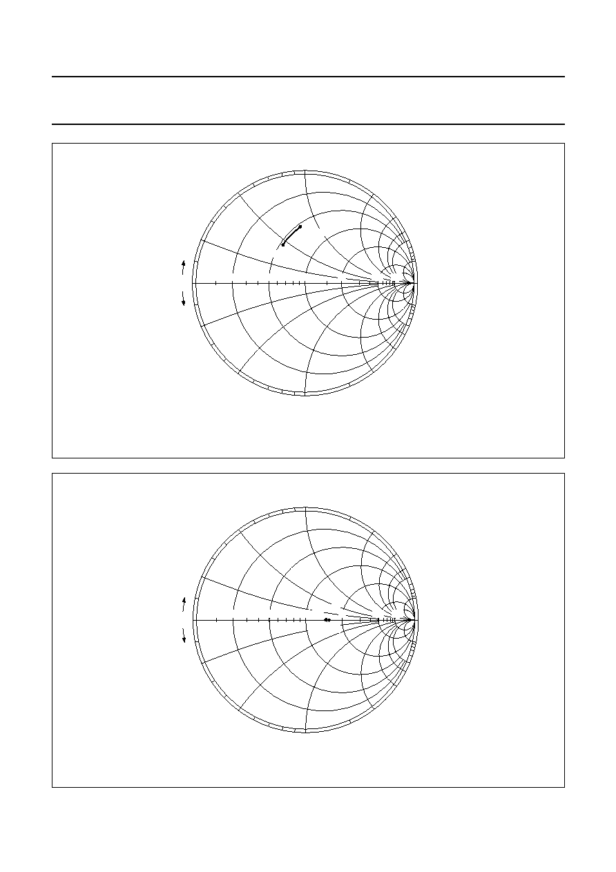
Fig.7 Input admittance (S
11
) of the VHF mixer input (40 to 400 MHz); Y
0
= 20 mS.
2001 Aug 22
22
Philips Semiconductors
Product specification
5 V mixers/oscillators and synthesizers for
cable TV and VCR 2-band tuners
TDA6502; TDA6502A;
TDA6503; TDA6503A
handbook, full pagewidth
0.2
0.5
1
2
5
10
0.2
0.5
1
2
5
10
0
+
j
-
j
FCE529
0.5
1
0.2
10
5
2
860 MHz
350 MHz
Fig.8 Input impedance (S
11
) of the UHF mixer input (350 to 860 MHz); Z
0
= 50
.
handbook, full pagewidth
0.2
0.5
1
2
5
10
0.2
0.5
1
2
5
10
0
+
j
-
j
FCE530
0.5
1
0.2
10
5
2
20 MHz
100 MHz
Fig.9 Output impedance (S
22
) of the IF amplifier (20 to 60 MHz); Z
0
= 50
.

2001 Aug 22
23
Philips Semiconductors
Product specification
5 V mixers/oscillators and synthesizers for
cable TV and VCR 2-band tuners
TDA6502; TDA6502A;
TDA6503; TDA6503A
12 TIMING CHARACTERISTICS
SYMBOL
PARAMETER
CONDITIONS
MIN.
TYP.
MAX.
UNIT
3-wire bus timing
t
HIGH
clock HIGH time
see Fig.10
2
-
-
µ
s
t
SU;DA
data set-up time
see Fig.10
2
-
-
µ
s
t
HD;DA
data hold time
see Fig.10
2
-
-
µ
s
t
SU;ENCL
enable-to-clock set-up time
see Fig.10
10
-
-
µ
s
t
HD;ENDA
enable-to-data hold time
see Fig.10
2
-
-
µ
s
t
EN
enable time between two transmissions
see Fig.11
10
-
-
µ
s
t
HD;ENCL
enable-to-clock active edge hold time
see Fig.11
6
-
-
µ
s
handbook, full pagewidth
FCE575
tHIGH
tHD;DA
tHD;ENDA
tSU;DA
tSU;ENCL
MSB
LSB
DA
CL
CE
INVALID
DATA
INVALID
DATA
Fig.10 Timing diagram for 3-wire bus; DA, CL and CE.
handbook, halfpage
FCE576
tEN
tHD;ENCL
CE
CL
Fig.11 Timing diagram for 3-wire bus; CE and CL.

2001 Aug 22
24
Philips Semiconductors
Product specification
5 V mixers/oscillators and synthesizers for
cable TV and VCR 2-band tuners
TDA6502; TDA6502A;
TDA6503; TDA6503A
13 TEST AND APPLICATION INFORMATION
13.1
Test circuits
handbook, full pagewidth
FCE577
50
27
50
50
V
VHFIN
IFOUT
e
Vmeas
RMS
voltmeter
spectrum
analyzer
Vo
Vi
D.U.T.
V'meas
signal
source
Fig.12 Gain measurement in VHF band.
Z
i
>> 50
V
i
= 2
◊
V
meas
= 80 dB
µ
V
V
i
= V
meas
+ 6 dB = 80 dB
µ
V
V
o
= V'
meas
◊
G
v
= 20 log
50
27
+
50
-------------------
V
o
V
i
------
handbook, full pagewidth
FCE578
L1
C2
C1
PCB
plug
plug
BNC
BNC
RIM-RIM
I1
C4
C3
PCB
RIM-RIM
I3
I2
(a)
(b)
Fig.13 Input circuit for optimum noise figure in VHF band.
(b) For f
RF
= 150 MHz:
mixer A frequency response measured = 150.3 MHz, loss = 1.3 dB
image suppression = 13 dB
C3 = 5 pF
C4 = 25 pF
l2 = 30 cm semi rigid RIM cable (33 dB/100 m, 50
and 96 pF/m).
l3 = 5 cm semi rigid RIM cable (33 dB/100 m, 50
and 96 pF/m).
(a) For f
RF
= 50 MHz:
mixer A frequency response measured = 57 MHz, loss = 0 dB
image suppression = 16 dB
C1 = 9 pF
C2 = 15 pF
L1 = 7 turns (
5.5 mm, wire
= 0.5 mm)
l1 = 5 cm semi rigid RIM cable (33 dB/100 m, 50
and 96 pF/m).

2001 Aug 22
25
Philips Semiconductors
Product specification
5 V mixers/oscillators and synthesizers for
cable TV and VCR 2-band tuners
TDA6502; TDA6502A;
TDA6503; TDA6503A
handbook, full pagewidth
FCE579
27
VHFIN
IFOUT
D.U.T.
NOISE
SOURCE
NOISE
FIGURE
METER
BNC
RIM
INPUT
CIRCUIT
NF = NF
meas
-
loss (of input circuit) (dB).
Fig.14 Noise figure (NF) measurement in VHF band.
handbook, full pagewidth
FCE580
50
50
27
50
50
45.75 MHz
V
VHFIN
IFOUT
A
B
C
D
HYBRID
ew
eu
18 dB
attenuator
Vmeas
RMS
voltmeter
modulation
analyzer
unwanted
signal
source
wanted
signal
source
AM = 30%
2 kHz
Vo
FILTER
D.U.T.
Fig.15 Cross modulation measurement in VHF band.
V
o
= V
meas
◊
Wanted output signal at f
RF(w)
= 55.25 (361.25) MHz; V
o(w)
= 100 dB
µ
V.
Measuring the level of the unwanted output signal V
o(u)
causing 0.3% AM modulation in the wanted output signal; f
RF(u)
= 59.75 (366.75) MHz.
f
OSC
= 101 (407) MHz.
Filter characteristics: f
c
= 45.75 MHz, f
-
3dB(BW)
= 1.4 MHz, f
-
30dB(BW)
= 3.1 MHz.
50
27
+
50
-------------------

2001 Aug 22
26
Philips Semiconductors
Product specification
5 V mixers/oscillators and synthesizers for
cable TV and VCR 2-band tuners
TDA6502; TDA6502A;
TDA6503; TDA6503A
handbook, full pagewidth
FCE581
UHFIN2
Vi
50
27
50
50
V
UHFIN1 IFOUT
e
Vmeas
RMS
voltmeter
spectrum
analyzer
Vo
D.U.T.
V'meas
signal
source
50
A
B
C
D
HYBRID
Fig.16 Gain (G
v
) measurement in UHF band.
Loss (in hybrid) = 1 dB.
V
i
= V
meas
-
loss (in hybrid) = 70 dB
µ
V.
V
o
= V'
meas
◊
G
v
= 20 log
50
27
+
50
-------------------
V
o
V
i
------
handbook, full pagewidth
FCE582
27
UHFIN
UHFIN
IFOUT
D.U.T.
NOISE
SOURCE
NOISE
FIGURE
METER
50
A
B
C
D
HYBRID
Fig.17 Noise figure (NF) measurement in bands UHF.
Loss (in hybrid) = 1 dB.
NF = NF
meas
-
loss (in hybrid).

2001 Aug 22
27
Philips Semiconductors
Product specification
5 V mixers/oscillators and synthesizers for
cable TV and VCR 2-band tuners
TDA6502; TDA6502A;
TDA6503; TDA6503A
handbook, full pagewidth
50
50
50
50
ew
eu
unwanted
signal
source
wanted
signal
source
AM = 30%
2 kHz
FCE583
27
50
45.75 MHz
V
UHFIN
UHFIN
IFOUT
A
B
C
D
HYBRID
A
B
C
D
HYBRID
18 dB
attenuator
Vmeas
RMS
voltmeter
modulation
analyzer
Vo
FILTER
D.U.T.
Fig.18 Cross modulation measurement in UHF band.
V
o
= V
meas
◊
Wanted output signal at f
RF(w)
= 367.25 (801.25) MHz; V
o(w)
= 100 dB
µ
V.
Measuring the level of the unwanted output signal V
o(u)
causing 0.3% AM modulation in the wanted output signal; f
RF(u)
= 371.25 (805.75) MHz.
f
OSC
= 413 (847) MHz.
Filter characteristics: f
c
= 45.75 MHz, f
-
3dB(BW)
= 1.4 MHz, f
-
30dB(BW)
= 3.1 MHz.
50
27
+
50
-------------------

2001
Aug
22
28
Philips Semiconductors
Product specification
5 V mix
ers/oscillators and synthesiz
ers f
o
r
cab
le TV and VCR 2-band tuners
TD
A6502; TD
A6502A;
TD
A6503; TD
A6503A
This text is here in white to force landscape pages to be rotated correctly when browsing through the pdf in the Acrobat reader.This text is here in
_
white to force landscape pages to be rotated correctly when browsing through the pdf in the Acrobat reader.This text is here inThis text is here in
white to force landscape pages to be rotated correctly when browsing through the pdf in the Acrobat reader. white to force landscape pages to be ...
13.2
Measurement cir
cuit
handbook, full pagewidth
FCE481
LED
LED
LED
LED
C1
C4
C5
C2
C3
4.7 nF
4.7 nF
4.7 nF
1(28)
2(27)
3(26)
4(25)
5(24)
6(23)
W1
W3
W2
15 pF
15 pF
L4
UHFIN1
UHFIN2
VHFIN
RFGND
IFFIL1
IFFIL2
PVHFL
PVHFH
PUHF
FMST
CE/AS
DA
CP
Y1
VT
XTAL
VCC
VCC
IFOUT
CL
SW
R15
R16
R17
R18
D4
D5
D6
D7
7(22)
8(21)
9(20)
10(19)
11(18)
12(17)
13(16)
14(15)
15(14)
16(13)
17(12)
18(11)
19(10)
20(9)
21(8)
22(7)
23(6)
24(5)
25(4)
26(3)
27(2)
28(1)
CON4
CON3
CON1
open for 3-wire
for test purpose only
for test purpose only
for test
purpose only
VCC
01 02
02 01
03
03
04
04
05 06
R24
R22
TDA6502/2A
(TDA6503/3A)
R12
R14
R10
R9
R8
R6 5.6
R5
R4
R3
R7
R2 27
R11
R13
R25
R26
TR1
BC847B
C27
10
µ
F
(16 V)
C26
10
µ
F
(16 V)
TR2
BC847B
68 k
1 k
LOCK
LOCK/ADC
J2
+
5 V
+
5 V
+
33 V
VS
LOCK
EN/AS
D
ATA
GND
CLOCK
GND
J3
C22
330 pF
C23
C21
C18 4.7 nF
C16
L1
L3
L5
L2
C10 1.2 pF
C11 1.2 pF
C13
C9 1.2 pF
C8 1.2 pF
C14
D3
D2
D1
C17
C15
C12
27 pF
C19 4.7 nF
C20
100 nF
10 nF
18 pF
4.7 nF
2 pF
4.7 nF
VHF-LOW
VHF-HIGH
BA792
BB178
BB179
OSCGND
VHFOSCIB
UHFOSCIB1
UHFOSCIB2
UHFOSCOC1
UHFOSCOC2
VHFOSCOC
GND
J1
RIPPLE
6.8 k
22 k
22 k
22 k
3.9 k
3.9 k
22 k
12 k
2.2 k
330
R21
330
R19
330
R20
330
330
330
330
330
680
27
82 pF
2 pF
10 k
Fig.19 Measurement circuit.
The pin numbers in parenthesis refer to the TDA6503 and TDA6503A.

2001 Aug 22
29
Philips Semiconductors
Product specification
5 V mixers/oscillators and synthesizers for
cable TV and VCR 2-band tuners
TDA6502; TDA6502A;
TDA6503; TDA6503A
Table 13 Capacitors (all SMD and NP0)
Table 14 Resistors (all SMD)
Table 15 Diodes and ICs
Table 16 Coils (note 1)
Note
1. Wire size is 0.4 mm.
Table 17 Transformer (note 1)
Note
1. Coil type: TOKO 7kN; material: 113 kN; screw core:
03-0093; pot core: 04-0026.
Table 18 Crystal
COMPONENT
VALUE
C1
4.7 nF
C2
4.7 nF
C3
4.7 nF
C4
15 pF
C5
15 pF
C8
1.2 pF (N750)
C9
1.2 pF (N750)
C10
1.2 pF(N750)
C11
1.2 pF (N750)
C12
27 pF (N750)
C13
2 pF (N750)
C14
2 pF (N750)
C15
82 pF (N750)
C16
4.7 nF
C17
4.7 nF
C18
4.7 nF
C19
4.7 nF
C20
18 pF
C21
100 nF
C22
330 pF
C23
10 nF
C26
10
µ
F (16 V, electrolytic)
C27
10
µ
F (16 V, electrolytic)
COMPONENT
VALUE
R2
27
R3
22 k
R4
22 k
R5
22 k
R6
5.6
R7
10 k
R8
680
R9
3.9 k
R10
3.9 k
R11
27
R12
12 k
R13
22 k
R14
2.2 k
R15
330
R16
330
R17
330
R18
330
R19
330
R20
330
R21
330
R22
330
R24
68 k
R25
1 k
R26
6.8 k
COMPONENT
VALUE
D1
BB179
D2
BB178
D3
BA792
IC
TDA6502; TDA6502A
TDA6503; TDA6503A
COMPONENT
VALUE
L1
1.5 turns; diameter 1.5 mm
L2
2.5 turns; diameter 2.5 mm
L3
7.5 turns; diameter 3.0 mm
L5
7.5 turns; diameter 2.5 mm
COMPONENT
VALUE
L4
2
◊
5 turns
COMPONENT
VALUE
Y1
4 MHz
COMPONENT
VALUE

2001 Aug 22
30
Philips Semiconductors
Product specification
5 V mixers/oscillators and synthesizers for
cable TV and VCR 2-band tuners
TDA6502; TDA6502A;
TDA6503; TDA6503A
Table 19 Transistors
13.3
Tuning amplifier
The tuning amplifier is capable of driving the varicap
voltage without an external transistor. The tuning voltage
output must be connected to an external load of 22 k
which is connected to the tuning voltage supply rail.
The loop filter design depends on the oscillator
characteristics and the selected reference frequency.
13.4
Crystal oscillator
The crystal oscillator uses a 4 MHz crystal connected in
series with an 18 pF capacitor thereby operating in the
series resonance mode. Connecting the crystal to the
ground is preferred, but it can also be connected to the
supply voltage.
13.5
Examples of I
2
C-bus data format sequences for
TDA6502 and TDA6503
Tables 20 to 24 show the various write sequences where:
S = START bit
A = acknowledge bit
P = STOP bit.
Conditions:
f
xtal
= 4 MHz
N = 1600
f
osc
= 100 MHz
f
step
= 62.5 kHz
Port register VHFL is `on' to switch-on band VHF low
Port register FMST is `on' to switch-on an FM sound trap
I
CP
= 280
µ
A.
COMPONENT
VALUE
TR1
BC847B
TR2
BC847B
13.5.1
W
RITE SEQUENCES TO REGISTER
C2
Table 20 Complete sequence with first the divider bytes (first data bit = 0)
Table 21 Complete sequence with first the control and band-switch bytes (first data bit = 1)
Table 22 Sequence with divider bytes only (first data bit = 0)
Table 23 Sequence with control and band-switch bytes only (first data bit = 1)
Table 24 Sequence with control byte only (first data bit = 1)
START
ADDRESS
BYTE
ACK
DIVIDER
BYTE 1
ACK
DIVIDER
BYTE 2
ACK
CONTROL
BYTE
ACK
BAND-
SWITCH
BYTE
ACK
STOP
S
C2
A
06
A
40
A
CE
A
09
A
P
START
ADDRESS
BYTE
ACK
CONTROL
BYTE
ACK
BAND-
SWITCH
BYTE
ACK
DIVIDER
BYTE 1
ACK
DIVIDER
BYTE 2
ACK
STOP
S
C2
A
CE
A
09
A
06
A
40
A
P
START
ADDRESS BYTE
ACK
DIVIDER BYTE 1
ACK
DIVIDER BYTE 2
ACK
STOP
S
C2
A
06
A
40
A
P
START
ADDRESS BYTE
ACK
CONTROL BYTE
ACK
BAND-SWITCH BYTE
ACK
STOP
S
C2
A
CE
A
09
A
P
START
ADDRESS BYTE
ACK
CONTROL BYTE
ACK
STOP
S
C2
A
CE
A
P

2001 Aug 22
31
Philips Semiconductors
Product specification
5 V mixers/oscillators and synthesizers for
cable TV and VCR 2-band tuners
TDA6502; TDA6502A;
TDA6503; TDA6503A
13.5.2
R
EAD SEQUENCES FROM REGISTER
C3
Tables 25 and 26 show the various read sequences where:
S = START bit
A = acknowledge bit
XX = read status byte
X = no acknowledge from the master means end of sequence
P = STOP bit
Table 25 One status byte acquisition
Table 26 Two status bytes acquisition
13.6
Examples of 3-wire bus data format sequences for TDA6502 and TDA6503
13.6.1
18-
BIT SEQUENCE
Conditions:
f
osc
= 800 MHz
Port register PUHF is `on'.
Table 27 18-bit sequence
The reference divider is automatically set to 64 assuming that bit RSB has been set to logic 1 at power-on. If bit RSB has
been set to logic 0, in a previous 27-bit sequence, the reference divider will still be set at 80. In this event, the 18-bit
sequence has to be adapted to the 80 divider ratio.
13.6.2
19-
BIT SEQUENCE
Conditions:
f
osc
= 650 MHz
Port register PUHF is `on'.
Table 28 19-bit sequence
The reference divider is automatically set to 128 assuming that bit RSB has been set to logic 1 at power-on. If bit RSB
has been set to logic 0 in a previous 27-bit sequence, the reference divider will still be set at 80. In this event, the 19-bit
sequence has to be adapted to the 80 divider ratio.
START
ADDRESS BYTE
ACK
STATUS BYTE
ACK
STOP
S
C3
A
XX
X
P
START
ADDRESS BYTE
ACK
STATUS BYTE
ACK
STATUS BYTE
ACK
STOP
S
C3
A
XX
A
XX
X
P
PUHF FMST PVHFH PVHFL
N13
N12
N11
N10
N9
N8
N7
N6
N5
N4
N3
N2
N1
N0
1
0
0
0
1
1
1
0
0
1
0
0
0
0
0
0
0
0
PUHF FMST PVHFH PVHFL
N14
N13
N12
N11
N10
N9
N8
N7
N6
N5
N4
N3
N2
N1
N0
1
0
0
0
1
0
1
0
0
0
1
0
1
0
0
0
0
0
0

2001 Aug 22
32
Philips Semiconductors
Product specification
5 V mixers/oscillators and synthesizers for
cable TV and VCR 2-band tuners
TDA6502; TDA6502A;
TDA6503; TDA6503A
13.6.3
27-
BIT SEQUENCE
Conditions:
f
osc
= 750 MHz
Port register PUHF is `on'
Reference divider is set at 80
I
CP
= 60
µ
A
No test function.
Table 29 27-bit sequence
To change the oscillator frequency to 600 MHz in 50 kHz steps a 19-bit sequence or an 18-bit sequence can be used.
The charge pump current remains at 60
µ
A.
Table 30 Changing frequency with a 19-bit sequence
Table 31 Changing frequency with an 18-bit sequence
PORT BITS
FREQUENCY DATA BITS
CONTROL DATA BITS
14 13 12 11 10
9
8
7
6
5
4
3
2
1
0
X CP T2 T1 T0 RSA RSB OS
1
0
0
0
0
1
1
1
0
1
0
1
0
0
1
1
0
0
0
1
0
0
0
1
0
0
0
PORT BITS
FREQUENCY DATA BITS
14
13
12
11
10
9
8
7
6
5
4
3
2
1
0
1
0
0
0
0
1
0
1
1
1
0
1
1
1
0
0
0
0
0
PORT BITS
FREQUENCY DATA BITS
13
12
11
10
9
8
7
6
5
4
3
2
1
0
1
0
0
0
1
0
1
1
1
0
1
1
1
0
0
0
0
0

2001 Aug 22
33
Philips Semiconductors
Product specification
5 V mixers/oscillators and synthesizers for
cable TV and VCR 2-band tuners
TDA6502; TDA6502A;
TDA6503; TDA6503A
14 INTERNAL PIN CONFIGURATION
SYMBOL
PIN
DC VOLTAGE
(AVERAGE VALUE)
(1)
EQUIVALENT CIRCUIT
(2)
TDA6502;
TDA6502A
TDA6503;
TDA6503A
VHF
UHF
UHFIN1
1
28
-
1.0 V
UHFIN2
2
27
-
1.0 V
VHFIN
3
26
1.8 V
-
RFGND
4
25
0.0 V
0.0 V
IFFIL1
5
24
3.6 V
3.6 V
IFFIL2
6
23
3.6 V
3.6 V
PVHFL
7
22
n.a. or 4.8 V
n.a.
PVHFH
8
21
4.8 V or n.a.
n.a.
PUHF
9
20
n.a.
4.8 V
FMST
10
19
n.a. or 4.8 V n.a. or 4.8 V
FCE584
1
2
(27)
(28)
FCE585
3
(26)
FCE586
4
(25)
FCE587
6
5
(23)
(24)
FCE588
7
(22)
9
(20)
10
(19)
8
(21)

2001 Aug 22
34
Philips Semiconductors
Product specification
5 V mixers/oscillators and synthesizers for
cable TV and VCR 2-band tuners
TDA6502; TDA6502A;
TDA6503; TDA6503A
SW
11
18
5.0 V
5.0 V
CE/AS
12
17
1.25 V
1.25 V
DA
13
16
-
-
CL
14
15
-
-
LOCK/ADC
15
14
4.6 V
4.6 V
SYMBOL
PIN
DC VOLTAGE
(AVERAGE VALUE)
(1)
EQUIVALENT CIRCUIT
(2)
TDA6502;
TDA6502A
TDA6503;
TDA6503A
VHF
UHF
FCE189
11
(18)
FCE191
12
(17)
FCE190
13
(16)
FCE192
14
(15)
FCE193
15
(14)

2001 Aug 22
35
Philips Semiconductors
Product specification
5 V mixers/oscillators and synthesizers for
cable TV and VCR 2-band tuners
TDA6502; TDA6502A;
TDA6503; TDA6503A
CP
16
13
1 V
1 V
VT
17
12
V
VT
V
VT
XTAL
18
11
2.6 V
2.6 V
V
CC
19
10
5.0 V
5.0 V
supply voltage
IFOUT
20
9
2.1 V
2.1 V
GND
21
8
0.0 V
0.0 V
SYMBOL
PIN
DC VOLTAGE
(AVERAGE VALUE)
(1)
EQUIVALENT CIRCUIT
(2)
TDA6502;
TDA6502A
TDA6503;
TDA6503A
VHF
UHF
16
(13)
FCE194
17
FCE589
(12)
FCE590
18
(11)
FCE591
20
(9)
FCE592
21
(8)

2001 Aug 22
36
Philips Semiconductors
Product specification
5 V mixers/oscillators and synthesizers for
cable TV and VCR 2-band tuners
TDA6502; TDA6502A;
TDA6503; TDA6503A
Notes
1. Measured in circuit of Fig.19.
2. The pin numbers in parenthesis represent the TDA6503 and TDA6503A.
OSCGND
23
6
0.0 V
0.0 V
VHFOSCIB
22
7
1.8 V
-
VHFOSCOC
24
5
3.0 V
-
UHFOSCIB1
25
4
-
1.9 V
UHFOSCOC1
26
3
-
2.9 V
UHFOSCOC2
27
2
-
2.9 V
UHFOSCIB2
28
1
-
1.9 V
SYMBOL
PIN
DC VOLTAGE
(AVERAGE VALUE)
(1)
EQUIVALENT CIRCUIT
(2)
TDA6502;
TDA6502A
TDA6503;
TDA6503A
VHF
UHF
FCE593
23
(6)
FCE594
22
24
(7)
(5)
FCE595
25
26
28
27
(1)
(2)
(3)
(4)

2001 Aug 22
37
Philips Semiconductors
Product specification
5 V mixers/oscillators and synthesizers for
cable TV and VCR 2-band tuners
TDA6502; TDA6502A;
TDA6503; TDA6503A
15 PACKAGE OUTLINE
UNIT
A
1
A
2
A
3
b
p
c
D
(1)
E
(1)
(1)
e
H
E
L
L
p
Q
Z
y
w
v
REFERENCES
OUTLINE
VERSION
EUROPEAN
PROJECTION
ISSUE DATE
IEC
JEDEC
EIAJ
mm
0.21
0.05
1.80
1.65
0.38
0.25
0.20
0.09
10.4
10.0
5.4
5.2
0.65
1.25
7.9
7.6
0.9
0.7
1.1
0.7
8
0
o
o
0.13
0.1
0.2
DIMENSIONS (mm are the original dimensions)
Note
1. Plastic or metal protrusions of 0.20 mm maximum per side are not included.
1.03
0.63
SOT341-1
MO-150
95-02-04
99-12-27
X
w
M
A
A
1
A
2
b
p
D
H
E
L
p
Q
detail X
E
Z
e
c
L
v
M
A
(A )
3
A
1
14
28
15
0.25
y
pin 1 index
0
2.5
5 mm
scale
SSOP28: plastic shrink small outline package; 28 leads; body width 5.3 mm
SOT341-1
A
max.
2.0

2001 Aug 22
38
Philips Semiconductors
Product specification
5 V mixers/oscillators and synthesizers for
cable TV and VCR 2-band tuners
TDA6502; TDA6502A;
TDA6503; TDA6503A
16 SOLDERING
16.1
Introduction to soldering surface mount
packages
This text gives a very brief insight to a complex technology.
A more in-depth account of soldering ICs can be found in
our
"Data Handbook IC26; Integrated Circuit Packages"
(document order number 9398 652 90011).
There is no soldering method that is ideal for all surface
mount IC packages. Wave soldering can still be used for
certain surface mount ICs, but it is not suitable for fine pitch
SMDs. In these situations reflow soldering is
recommended.
16.2
Reflow soldering
Reflow soldering requires solder paste (a suspension of
fine solder particles, flux and binding agent) to be applied
to the printed-circuit board by screen printing, stencilling or
pressure-syringe dispensing before package placement.
Several methods exist for reflowing; for example,
convection or convection/infrared heating in a conveyor
type oven. Throughput times (preheating, soldering and
cooling) vary between 100 and 200 seconds depending
on heating method.
Typical reflow peak temperatures range from
215 to 250
∞
C. The top-surface temperature of the
packages should preferable be kept below 220
∞
C for
thick/large packages, and below 235
∞
C for small/thin
packages.
16.3
Wave soldering
Conventional single wave soldering is not recommended
for surface mount devices (SMDs) or printed-circuit boards
with a high component density, as solder bridging and
non-wetting can present major problems.
To overcome these problems the double-wave soldering
method was specifically developed.
If wave soldering is used the following conditions must be
observed for optimal results:
∑
Use a double-wave soldering method comprising a
turbulent wave with high upward pressure followed by a
smooth laminar wave.
∑
For packages with leads on two sides and a pitch (e):
≠ larger than or equal to 1.27 mm, the footprint
longitudinal axis is preferred to be parallel to the
transport direction of the printed-circuit board;
≠ smaller than 1.27 mm, the footprint longitudinal axis
must be parallel to the transport direction of the
printed-circuit board.
The footprint must incorporate solder thieves at the
downstream end.
∑
For packages with leads on four sides, the footprint must
be placed at a 45
∞
angle to the transport direction of the
printed-circuit board. The footprint must incorporate
solder thieves downstream and at the side corners.
During placement and before soldering, the package must
be fixed with a droplet of adhesive. The adhesive can be
applied by screen printing, pin transfer or syringe
dispensing. The package can be soldered after the
adhesive is cured.
Typical dwell time is 4 seconds at 250
∞
C.
A mildly-activated flux will eliminate the need for removal
of corrosive residues in most applications.
16.4
Manual soldering
Fix the component by first soldering two
diagonally-opposite end leads. Use a low voltage (24 V or
less) soldering iron applied to the flat part of the lead.
Contact time must be limited to 10 seconds at up to
300
∞
C.
When using a dedicated tool, all other leads can be
soldered in one operation within 2 to 5 seconds between
270 and 320
∞
C.

2001 Aug 22
39
Philips Semiconductors
Product specification
5 V mixers/oscillators and synthesizers for
cable TV and VCR 2-band tuners
TDA6502; TDA6502A;
TDA6503; TDA6503A
16.5
Suitability of surface mount IC packages for wave and reflow soldering methods
Notes
1. All surface mount (SMD) packages are moisture sensitive. Depending upon the moisture content, the maximum
temperature (with respect to time) and body size of the package, there is a risk that internal or external package
cracks may occur due to vaporization of the moisture in them (the so called popcorn effect). For details, refer to the
Drypack information in the
"Data Handbook IC26; Integrated Circuit Packages; Section: Packing Methods".
2. These packages are not suitable for wave soldering as a solder joint between the printed-circuit board and heatsink
(at bottom version) can not be achieved, and as solder may stick to the heatsink (on top version).
3. If wave soldering is considered, then the package must be placed at a 45
∞
angle to the solder wave direction.
The package footprint must incorporate solder thieves downstream and at the side corners.
4. Wave soldering is only suitable for LQFP, TQFP and QFP packages with a pitch (e) equal to or larger than 0.8 mm;
it is definitely not suitable for packages with a pitch (e) equal to or smaller than 0.65 mm.
5. Wave soldering is only suitable for SSOP and TSSOP packages with a pitch (e) equal to or larger than 0.65 mm; it is
definitely not suitable for packages with a pitch (e) equal to or smaller than 0.5 mm.
PACKAGE
SOLDERING METHOD
WAVE
REFLOW
(1)
BGA, HBGA, LFBGA, SQFP, TFBGA
not suitable
suitable
HBCC, HLQFP, HSQFP, HSOP, HTQFP, HTSSOP, HVQFN, SMS
not suitable
(2)
suitable
PLCC
(3)
, SO, SOJ
suitable
suitable
LQFP, QFP, TQFP
not recommended
(3)(4)
suitable
SSOP, TSSOP, VSO
not recommended
(5)
suitable

2001 Aug 22
40
Philips Semiconductors
Product specification
5 V mixers/oscillators and synthesizers for
cable TV and VCR 2-band tuners
TDA6502; TDA6502A;
TDA6503; TDA6503A
17 DATA SHEET STATUS
Notes
1. Please consult the most recently issued data sheet before initiating or completing a design.
2. The product status of the device(s) described in this data sheet may have changed since this data sheet was
published. The latest information is available on the Internet at URL http://www.semiconductors.philips.com.
DATA SHEET STATUS
(1)
PRODUCT
STATUS
(2)
DEFINITIONS
Objective specification
Development
This data sheet contains data from the objective specification for product
development. Philips Semiconductors reserves the right to change the
specification in any manner without notice.
Preliminary specification
Qualification
This data sheet contains data from the preliminary specification.
Supplementary data will be published at a later date. Philips
Semiconductors reserves the right to change the specification without
notice, in order to improve the design and supply the best possible
product.
Product specification
Production
This data sheet contains data from the product specification. Philips
Semiconductors reserves the right to make changes at any time in order
to improve the design, manufacturing and supply. Changes will be
communicated according to the Customer Product/Process Change
Notification (CPCN) procedure SNW-SQ-650A.
18 DEFINITIONS
Short-form specification
The data in a short-form
specification is extracted from a full data sheet with the
same type number and title. For detailed information see
the relevant data sheet or data handbook.
Limiting values definition
Limiting values given are in
accordance with the Absolute Maximum Rating System
(IEC 60134). Stress above one or more of the limiting
values may cause permanent damage to the device.
These are stress ratings only and operation of the device
at these or at any other conditions above those given in the
Characteristics sections of the specification is not implied.
Exposure to limiting values for extended periods may
affect device reliability.
Application information
Applications that are
described herein for any of these products are for
illustrative purposes only. Philips Semiconductors make
no representation or warranty that such applications will be
suitable for the specified use without further testing or
modification.
19 DISCLAIMERS
Life support applications
These products are not
designed for use in life support appliances, devices, or
systems where malfunction of these products can
reasonably be expected to result in personal injury. Philips
Semiconductors customers using or selling these products
for use in such applications do so at their own risk and
agree to fully indemnify Philips Semiconductors for any
damages resulting from such application.
Right to make changes
Philips Semiconductors
reserves the right to make changes, without notice, in the
products, including circuits, standard cells, and/or
software, described or contained herein in order to
improve design and/or performance. Philips
Semiconductors assumes no responsibility or liability for
the use of any of these products, conveys no licence or title
under any patent, copyright, or mask work right to these
products, and makes no representations or warranties that
these products are free from patent, copyright, or mask
work right infringement, unless otherwise specified.

2001 Aug 22
41
Philips Semiconductors
Product specification
5 V mixers/oscillators and synthesizers for
cable TV and VCR 2-band tuners
TDA6502; TDA6502A;
TDA6503; TDA6503A
20 PURCHASE OF PHILIPS I
2
C COMPONENTS
Purchase of Philips I
2
C components conveys a license under the Philips' I
2
C patent to use the
components in the I
2
C system provided the system conforms to the I
2
C specification defined by
Philips. This specification can be ordered using the code 9398 393 40011.

2001 Aug 22
42
Philips Semiconductors
Product specification
5 V mixers/oscillators and synthesizers for
cable TV and VCR 2-band tuners
TDA6502; TDA6502A;
TDA6503; TDA6503A
NOTES

2001 Aug 22
43
Philips Semiconductors
Product specification
5 V mixers/oscillators and synthesizers for
cable TV and VCR 2-band tuners
TDA6502; TDA6502A;
TDA6503; TDA6503A
NOTES

© Koninklijke Philips Electronics N.V. 2001
SCA73
All rights are reserved. Reproduction in whole or in part is prohibited without the prior written consent of the copyright owner.
The information presented in this document does not form part of any quotation or contract, is believed to be accurate and reliable and may be changed
without notice. No liability will be accepted by the publisher for any consequence of its use. Publication thereof does not convey nor imply any license
under patent- or other industrial or intellectual property rights.
Philips Semiconductors ≠ a worldwide company
Contact information
For additional information please visit http://www.semiconductors.philips.com.
Fax: +31 40 27 24825
For sales offices addresses send e-mail to: sales.addresses@www.semiconductors.philips.com.
Printed in The Netherlands
753504/04/pp
44
Date of release:
2001 Aug 22
Document order number:
9397 750 08538