 | –≠–ª–µ–∫—Ç—Ä–æ–Ω–Ω—ã–π –∫–æ–º–ø–æ–Ω–µ–Ω—Ç: TDA6508TT | –°–∫–∞—á–∞—Ç—å:  PDF PDF  ZIP ZIP |

DATA SHEET
Product specification
Supersedes data of 2005 Feb 23
2005 Mar 25
INTEGRATED CIRCUITS
TDA6508; TDA6508A; TDA6509;
TDA6509A
3-band mixer/oscillator and PLL for
terrestrial tuners

2005 Mar 25
2
Philips Semiconductors
Product specification
3-band mixer/oscillator and PLL for
terrestrial tuners
TDA6508; TDA6508A;
TDA6509; TDA6509A
CONTENTS
1
FEATURES
2
APPLICATIONS
3
GENERAL DESCRIPTION
4
QUICK REFERENCE DATA
5
ORDERING INFORMATION
6
BLOCK DIAGRAM
7
PINNING
8
I
2
C-BUS DATA FORMAT
8.1
I
2
C-bus address selection
8.2
Write mode
8.3
Read mode
8.4
Power-on reset
9
LIMITING VALUES
10
HANDLING
11
THERMAL CHARACTERISTICS
12
CHARACTERISTICS
13
TEST AND APPLICATION INFORMATION
13.1
Measurement circuit
14
INTERNAL PIN CONFIGURATION
15
PACKAGE OUTLINES
16
SOLDERING
16.1
Introduction to soldering surface mount
packages
16.2
Reflow soldering
16.3
Wave soldering
16.4
Manual soldering
16.5
Suitability of surface mount IC packages for
wave and reflow soldering methods
17
DATA SHEET STATUS
18
DEFINITIONS
19
DISCLAIMERS

2005 Mar 25
3
Philips Semiconductors
Product specification
3-band mixer/oscillator and PLL for
terrestrial tuners
TDA6508; TDA6508A;
TDA6509; TDA6509A
1
FEATURES
∑
Single-chip 5 V mixer / oscillator and synthesizer for TV,
VCR tuners, DVD-R and PC TV.
∑
I
2
C bus protocol compatible with 3.3 V and 5 V
microcontrollers
≠ Address with 4 data bytes transmission (I
2
C-bus
`write' mode)
≠ Address with 1 status byte (I
2
C-bus `read' mode)
≠ 4 independent I
2
C-bus addresses.
∑
5 Positive-channel Metal Oxide Semiconductor (PMOS)
output ports
≠ 3 buffers for band selection (20 mA)
≠ 2 buffers for general purpose, e.g. FM sound trap
(5 mA).
∑
33 V tuning voltage output
∑
In-lock flag
∑
5-step analog-to-digital converter (3 bits in I
2
C-bus
mode)
∑
15-bit programmable divider
∑
Programmable reference divider ratio (64, 80 or 128)
∑
Programmable charge-pump current (20 or 100
µ
A)
∑
Balanced mixer with a common emitter input for LOW
band (single input)
∑
Balanced mixer with a common emitter input for MID
band (balanced input)
∑
Balanced mixer with a common base input for HIGH
band (balanced input)
∑
2-pin asymmetrical oscillator for LOW band
∑
2-pin symmetrical oscillator for MID band
∑
2-pin symmetrical oscillator for HIGH band
∑
External 4-pin IF filter between mixer output (medium
impedance) and IF amplifier input (high impedance)
∑
Weak signal booster (I
2
C controlled switchable gain
amplifier)
∑
Low power
∑
Low radiation
∑
Small size
∑
TDA6508; TDA6509: symmetrical IF amplifier output to
drive a SAW filter (1.25 k
)
∑
TDA6508A; TDA6509A: single-ended IF amplifier to
drive low ohmic load (75
).
2
APPLICATIONS
∑
3-band tuner for terrestrial TV, DVD-R, VCR and PC TV.
3
GENERAL DESCRIPTION
This device is a programmable 3-band mixer oscillator and
synthesizer intended for LOW, MID and HIGH band TV
and VCR tuners. It has three double balanced mixers and
three oscillators for the LOW, MID and HIGH band
respectively, a PLL synthesizer, and an IF amplifier. There
are four package variants: TDA6508, TDA6509,
TDA6508A and TDA6509A. Versions TDA6508; TDA6509
have a symmetrical IF amplifier; versions TDA6508A;
TDA6509A have an asymmetrical IF amplifier, (see Fig.1).
The common output of all three mixers can be connected,
via two output pins, to an external IF filter to enable
shunted IF bandpass and/or serial filtering for improved
signal handling. Two input pins are available for
connecting the output of the external filter to the input of
the IF amplifier. The mixer output has an impedance
of 300
. The IF amplifier input has an impedance
of 2.5 k
(5 pF).
The overall gain of the tuner can be increased at low signal
amplitude conditions to improve TV reception by activating
a weak signal booster via the I
2
C-bus.
There are five open-drain PMOS output ports; each port
has a different drive capability. I
2
C-bus bit P0 enables
port P0 (20 mA drain current) and the LOW band mixer
oscillator. Bit P1 enables port P1 (20 mA drain current)
and the MID band mixer oscillator. When ports P0 and P1
are both disabled, the HIGH band mixer oscillator is
enabled. Bit P2 enables port P2 (20 mA drain current).
Bit P3 enables port P3 (5 mA drain current) for general
use, and bit P4 enables port P4 (5 mA drain current) for
general use, and is also combined with the ADC input.
When the ports are used, the sum of the drain currents
must be limited to 30 mA.
The PLL synthesizer comprises a 15-bit programmable
divider, a crystal oscillator, programmable reference
divider, phase comparator (phase/frequency detector)
combined with a charge-pump which drives an internal
tuning amplifier and an output at pin CP. The CP signal
current can be integrated by connecting an external RC

2005 Mar 25
4
Philips Semiconductors
Product specification
3-band mixer/oscillator and PLL for
terrestrial tuners
TDA6508; TDA6508A;
TDA6509; TDA6509A
loop filter between pin CP and pin VTUNE as shown in
Fig.27. The tuning amplifier can supply up to 33 V (max.)
at pin VT for controlling any of the internal oscillators via
external tank circuits. The phase comparator can operate
at 62.5, 50 or 31.25 kHz with a 4 MHz crystal, depending
on the reference divider ratio of either 64, 80 or 128; see
Table 4. An externally sourced signal having a frequency
between 3.58 MHz and 4.43 MHz can be used as a
reference frequency for the internal crystal oscillator at any
of the reference divider ratios.
In test mode, port P3 will output either half the crystal
reference frequency (
1
/
2
f
ref
) or half the reference divider
frequency (
1
/
2
f
div
); see Table 5.
The device can be controlled according to the I
2
C-bus
format; see Table 1. The in-lock flag bit FL is set to logic 1
when the PLL is locked. This flag is read from the status
byte on pin SDA during a READ operation; see Table 6
and Table 7.
Automatic frequency control is provided using an internal
Analog-to-Digital Converter controlled by the voltage on
pin ADC. The ADC code is read during a READ operation;
see Table 8.
The device requires to be addressed by five sequential
serial bytes (including the address byte) via the I
2
C-bus to
set the crystal oscillator frequency, program the five ports
and to set the charge-pump current; see Table 1. The
address byte can have one of four possible device
addresses which are selected by applying a specific
voltage to pin AS; see Table 3.
4
QUICK REFERENCE DATA
Measured over full voltage and temperature ranges.
5
ORDERING INFORMATION
SYMBOL
PARAMETER
CONDITIONS
MIN.
TYP.
MAX.
UNIT
V
CC
supply voltage
4.5
5
5.5
V
I
CC
supply current
V
CC
= 5 V; all ports off
43
58
74
mA
f
xtal
crystal oscillator frequency
R
xtal
= 25
to 300
3.58
4.0
4.43
MHz
P
tot
total power dissipation
-
290
385
mW
T
stg
IC storage temperature
-
40
-
+
150
∞
C
T
amb
ambient temperature
-
20
-
+
85
∞
C
TYPE
NUMBER
PACKAGE
NAME
DESCRIPTION
VERSION
TDA6508TT
TSSOP32
plastic thin shrink small outline package; 32 leads body width 6.1 mm
SOT487-1
TDA6508ATT
TDA6509TT
TSSOP32
plastic thin shrink small outline package; 32 leads body width 6.1 mm
SOT487-1
TDA6509ATT
TDA6509HN
HVQFN32
plastic thermal enhanced very thin quad flat package; no leads;
32 terminals; body 5
◊
5
◊
0.85 mm
SOT617-1
TDA6509AHN
2005 Mar 25
5
Philips Semiconductors
Product specification
3-band mixer/oscillator and PLL for
terrestrial tuners
TDA6508; TDA6508A;
TDA6509; TDA6509A
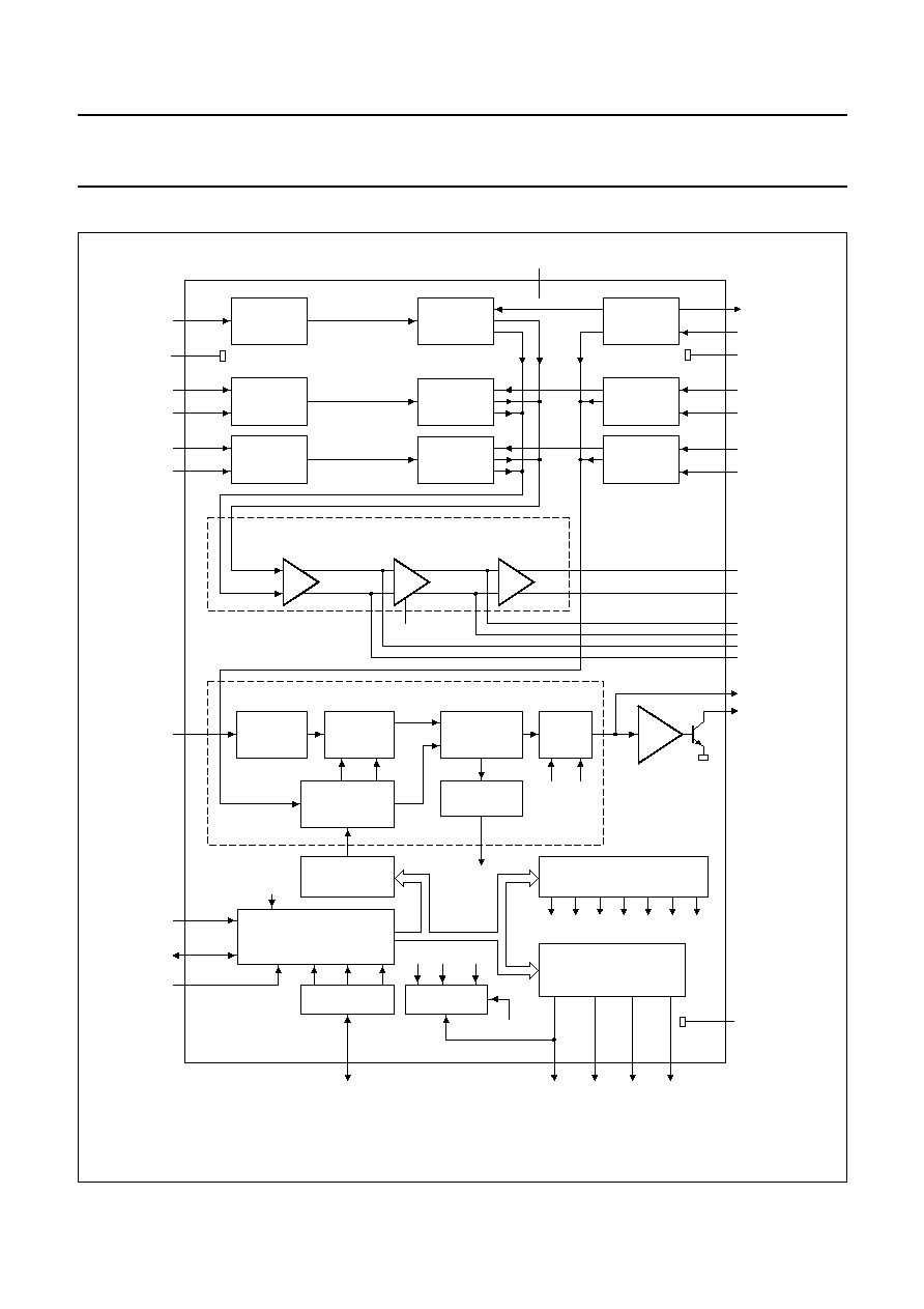
6
BLOCK DIAGRAM
mdb250
REFERENCE
DIVIDER
64, 80, 128
CRYSTAL
OSCILLATOR
4 MHz
15-BIT
PROGRAMMABLE
DIVIDER
15-BIT
FREQUENCY
REGISTER
PHASE
COMPARATOR
IN-LOCK
DETECTOR
CHARGE
PUMP
TUNE
AMP
FL
T0
T1
T2
CP
CP
T2
T1
T0 RSA RSB WSB
CONTROL
REGISTER
FL
I2C-BUS / 3-WIRE BUS
TRANSCEIVER
3-BIT ADC
PORT
REGISTER
FL
f
ref
f
ref
1/2f
div
f
div
GATE
RF INPUT
VHF
LOW BAND
VHF
LOW BAND
MIXER
VHF
LOW BAND
OSCILLATOR
RF INPUT
VHF
HIGH BAND
VHF
HIGH BAND
MIXER
VHF
HIGH BAND
OSCILLATOR
T0, T1, T2
RSA
RSB
LOW_RFIN
RF_GND
MID_RFIN1
MID_RFIN2
XTAL_REF
SCL
SDA
AS
V
CC
LOW_OSCOUT
LOW_OSCIN
OSC_GND
MID_OSCIN1
MID_OSCIN2
PLL_GND
P0
P1
P2
P3
ADC/P4
5 (28)
6 (27)
3 (30)
4 (29)
17
(16)
16 (17)
15 (18)
21 (12)
18 (15)
14 (19)
11 (22) 12 (21) 13 (20)
29 (4)
28 (5)
30 (3)
32 (1)
31 (2)
25 (8)
TDA6508
TDA6508A
(TDA6509)
(TDA6509A)
RF INPUT
UHF
BAND
UHF
MIXER
UHF
OSCILLATOR
HIGH_RFIN1
HIGH_RFIN2
HIGH_OSCIN1
HIGH_OSCIN2
IFAMP_OUT1
IFAMP_OUT2/
IF_GND
IFAMP_IN1
IFAMP_IN2
MIX_OUT1
MIX_OUT2
CP
VT
1 (32)
2 (31)
27 (6)
23 (10)
24 (9)
9 (24)
10 (23)
7 (26)
8 (25)
19 (14)
20 (13)
22 (11)
26 (7)
FILTER BUFFER
SYMMETRICAL/ASYMMETRICAL IFAMPLIFIER
PLL SYNTHESIZER
WEAK SIGNAL BOOSTER
SAW DRIVER
WSB
Fig.1 Block diagram.
(1) `A' versions only.
The pin numbers in parenthesis refer to versions TDA6509 and TDA6509A.

2005 Mar 25
6
Philips Semiconductors
Product specification
3-band mixer/oscillator and PLL for
terrestrial tuners
TDA6508; TDA6508A;
TDA6509; TDA6509A
7
PINNING
SYMBOL
PIN
DESCRIPTION
TDA6508;
TDA6508A
TDA6509;
TDA6509A
HIGH_RFIN1
1
32
HIGH band RF input 1
HIGH_RFIN2
2
31
HIGH band RF input 2
MID_RFIN1
3
30
MID band RF input 1
MID_RFIN2
4
29
MID band RF input 2
LOW_RFIN
5
28
LOW band RF input
RF_GND
6
27
RF ground
MIX_OUT1
7
26
mixer output 1 (to external IF filter)
MIX_OUT2
8
25
mixer IF output 2 (to external IF filter)
IFAMP_IN1
9
24
IF amplifier input 1 (from external IF filter)
IFAMP_IN2
10
23
IF amplifier input 2 (from external IF filter)
P2
11
22
HIGH band port output
P1
12
21
MID band port output
P0
13
20
LOW band port output
P3
14
19
general purpose port - test mode output
SDA
15
18
serial data input/output
SCL
16
17
serial clock input
XTAL_REF
17
16
crystal oscillator reference signal input
ADC/P4
18
15
ADC input/general purpose port output
CP
19
14
charge-pump output
VT
20
13
tuning voltage output
AS
21
12
address selection input
PLL_GND
22
11
PLL ground
IFAMP_OUT1
23
10
IF amplifier output 1
IFAMP_OUT2
24
9
IF amplifier output 2 (TDA6508 and TDA6509 only)
IF_GND
24
9
IF ground (TDA6508A and TDA6509A only)
V
CC
25
8
supply voltage
HIGH_OSCIN1
26
7
HIGH band oscillator input 1
HIGH_OSCIN2
27
6
HIGH band oscillator input 2
MID_OSCIN1
28
5
MID band oscillator input 1
MID_OSCIN2
29
4
MID band oscillator input 2
OSC_GND
30
3
oscillator ground
LOW_OSCOUT
31
2
LOW band oscillator output
LOW_OSCIN
32
1
LOW band oscillator input

2005 Mar 25
7
Philips Semiconductors
Product specification
3-band mixer/oscillator and PLL for
terrestrial tuners
TDA6508; TDA6508A;
TDA6509; TDA6509A
handbook, halfpage
TDA6508
TDA6508A
MDB226
1
2
3
4
5
6
7
8
9
10
11
12
13
14
15
16
HIGH_RFIN1
HIGH_RFIN2
MID_RFIN1
MID_RFIN2
LOW_RFIN
RF_GND
MIX_OUT1
MIX_OUT2
IFAMP_IN1
IFAMP_IN2
P2
P1
P0
P3
SDA
SCL
LOW_OSCIN
LOW_OSCOUT
OSC_GND
MID_OSCIN2
MID_OSCIN1
HIGH_OSCIN2
HIGH_OSCIN1
VCC
IFAMP_OUT2/IF_GND
IFAMP_OUT1
PLL_GND
AS
VT
CP
ADC/P4
XTAL_REF
32
31
30
29
28
27
26
25
24
23
22
21
20
19
18
17
Fig.2
Pin configuration for TDA6508 and
TDA6508A (TSSOP32).
handbook, halfpage
TDA6509
TDA6509A
MDB227
1
2
3
4
5
6
7
8
9
10
11
12
13
14
15
16
LOW_OSCIN
LOW_OSCOUT
OSC_GND
MID_OSCIN2
MID_OSCIN1
HIGH_OSCIN2
HIGH_OSCIN1
VCC
IF_GND/IFAMP_OUT2
IFAMP_OUT1
PLL_GND
AS
VT
CP
ADC/P4
XTAL_REF
HIGH_RFIN1
HIGH_RFIN2
MID_RFIN1
MID_RFIN2
LOW_RFIN
RF_GND
MIX_OUT1
MIX_OUT2
IFAMP_IN1
IFAMP_IN2
P2
P1
P0
P3
SDA
SCL
32
31
30
29
28
27
26
25
24
23
22
21
20
19
18
17
Fig.3 Pin configuration for TDA6509 and TDA6509A
(TSSOP32).
2005 Mar 25
8
Philips Semiconductors
Product specification
3-band mixer/oscillator and PLL for
terrestrial tuners
TDA6508; TDA6508A;
TDA6509; TDA6509A
handbook, halfpage
IF_GND/IFAMP_OUT2
VT
PLL_GND
AS
IFAMP_OUT1
CP
XTAL_REF
ADC/P4
HIGH_RFIN1
LOW_RFIN
MID_RFIN1
MID_RFIN2
HIGH_RFIN2
RF_GND
MIX_OUT2
MIX_OUT1
TDA6509
TDA6509A
VCC
HIGH_OSCIN2
HIGH_OSCIN1
MID_OSCIN1
MID_OSCIN2
OSC_GND
LOW_OSCOUT
LOW_OSCIN
MDB225
SDA
SCL
P0
P3
P1
P2
IFAMP_IN2
IFAMP_IN1
2
1
3
4
5
6
7
16
14
12
15
13
11
10
9
25
28
26
27
29
30
31
32
8
24
23
21
22
20
19
18
17
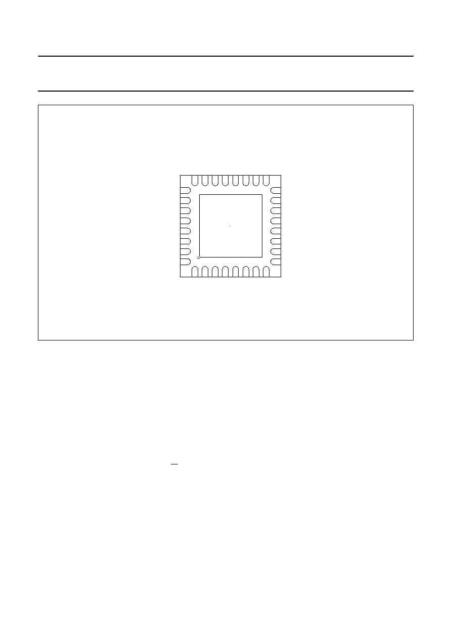
Fig.4 Pin configuration for TDA6509 and TDA6509A (HVQFN32).
8
I
2
C-BUS DATA FORMAT
8.1
I
2
C-bus address selection
The address byte ADB contains programmable module
address bits MA1 and MA0 which allow up to four
synthesizers to be used in the same system, and are
configured by applying one of four possible voltages on
pin AS; see Tables 1 and 2. For each voltage on pin AS,
the resultant values of bits MA1 and MA0 are shown in
Table 3.
8.2
Write mode
The write mode is defined by setting bit R/W to logic 0 in
address byte ADB; see Table 1.
Data bytes can be sent to the device after sending the first
address byte. Four data bytes are required to fully program
the device.
The bus transceiver has an auto-increment facility which
allows the device to be programmed by one transmission
(address byte with 4 data bytes). The device can be
partially programmed provided that the first data byte
following the address byte is divider byte DB1 or control
byte CB.
The MSB of the first data byte DB1 indicates whether
frequency data (MSB = 0) or control and band switch data
will follow. Additional data bytes can be entered without the
need to re-address the device until an I
2
C-bus STOP
command is sent by the controller.
The frequency divider register is loaded after the 8th clock
pulse of byte DB2. The control register is loaded after the
8th clock pulse of byte CB, and the band switch register is
loaded after the 8th clock pulse of byte BB.

2005 Mar 25
9
Philips Semiconductors
Product specification
3-band mixer/oscillator and PLL for
terrestrial tuners
TDA6508; TDA6508A;
TDA6509; TDA6509A
Table 1
I
2
C-bus data format for write mode
Note
1. X = don't care.
Table 2
Function of write mode bits used in Table 1
Table 3
Module address selection bits
NAME
BYTE
BITS
(1)
MSB
LSB
Address byte
ADB
1
1
0
0
0
MA1
MA0
R/W = 0
Divider byte 1
DB1
0
N14
N13
N12
N11
N10
N9
N8
Divider byte 2
DB2
N7
N6
N5
N4
N3
N2
N1
N0
Control byte
CB
1
CP
T2
T1
T0
RSA
RSB
WSB
Band switch byte
BB
X
X
X
P4
P3
P2
P1
P0
BIT
FUNCTION
MA1 and MA0
module address; see Table 3
R/W
read/write mode; 0 = write mode
N14 to N0
programmable divider bits: N = N14
◊
2
14
+
N13
◊
2
13
+
...
+
N1
◊
2
1
+
N0
CP
charge-pump current control:
0: charge-pump current is 20
µ
A
1: charge-pump current is 100
µ
A
T2, T1 and T0
test mode; see Table 5
RSA and RSB
reference divider ratio; see Table 4
WSB
Weak Signal Booster control:
0: normal mode - no gain increase: external IF filter used
1: Weak Signal Booster activated: IF filter by-passed
P0, P1, P2, P3, P4
port P0 to P4 control:
0: corresponding port is off; high impedance state (default)
1: corresponding port is on.
MA1
MA0
VOLTAGE APPLIED TO PIN AS
0
0
0 V to 0.1V
CC
0
1
0.2V
CC
to 0.3V
CC
or open-circuit
1
0
0.4V
CC
to 0.6V
CC
1
1
0.9V
CC
to 1.0V
CC

2005 Mar 25
10
Philips Semiconductors
Product specification
3-band mixer/oscillator and PLL for
terrestrial tuners
TDA6508; TDA6508A;
TDA6509; TDA6509A
Table 4
Reference divider ratio selection bits
Note
1. Crystal oscillator frequency or externally sourced reference frequency of 4 MHz at pin XTAL_REF.
Table 5
Test mode selection bits
Notes
1. This is the default mode at power-on reset.
2.
1
/
2
f
div
is output from port P3 when the charge-pump is off.
3. Port P3 cannot be used when these test modes are active.
RSA
RSB
REFERENCE DIVIDER RATIO
FREQUENCY STEP (kHz)
(1)
X
0
80
50
0
1
128
31.25
1
1
64
62.5
T2
T1
T0
TEST MODE
0
0
0
normal mode (read and write mode bytes allowed)
0
0
1
normal mode (read and write mode bytes allowed)
(1)
0
1
0
charge-pump is off
(2)
0
1
1
byte BB ignored
1
1
0
charge-pump sinks current
1
1
1
charge-pump sources current
1
0
0
1
/
2
f
ref
is output from port P3
(3)
1
0
1
1
/
2
f
div
is output from port P3
(3)
8.3
Read mode
The read mode is defined by setting bit R/W to logic 1 in
address byte ADB; see Table 6.
After the slave address has been recognized, the device
generates an acknowledge pulse, and status byte SB is
transferred on the SDA line (MSB first). Data is valid on the
SDA line when pin SCL is HIGH. A second data byte can
be read from the device if the microcontroller generates an
acknowledge on the SDA line (master acknowledge).
End of transmission will occur if no master acknowledge is
asserted. The device will then release the data line to allow
the microcontroller to generate a STOP condition.
Bit POR is set to logic 1 at power-on. This bit is reset when
an end-of-data is detected by the device at the end of a
read sequence. Bit FL controls the PLL by indicating when
the loop is locked (bit FL = 1).
The internal ADC can be used to apply AFC information to
a microcontroller in the IF section of the television via
status byte bits A0, A1 and A2. Up to five voltage levels
can be applied to the ADC input pin ADC; the resultant
values of bits A2, A1 and A0 are shown in Table 8.
2005 Mar 25
11
Philips Semiconductors
Product specification
3-band mixer/oscillator and PLL for
terrestrial tuners
TDA6508; TDA6508A;
TDA6509; TDA6509A
Table 6
Read data format
Note
1. MSB is transmitted first.
Table 7
Description of the bits used in Table 6
Table 8
Digital outputs for analog to digital converter (note 1)
Note
1. Accuracy is
±
0.03
◊
V
CC
.
8.4
Power-on reset
The threshold level for the power-on reset supply voltage V
POR
is set to 3.2 V at room temperature. Below this threshold,
the device is reset to the power-on state.
The following actions take place In the power-on state:
∑
The charge-pump current is set to 100
µ
A
∑
Test bits T2, T1 and T0 are set to logic 001; the charge-pump can either sink or source current
∑
The Weak signal booster is disabled
∑
All ports are off and the HIGH band is selected by default.
NAME
BYTE
BIT
MSB
(1)
LSB
Address byte
ADB
1
1
0
0
0
MA1
MA0
R/W = 1
Status byte
SB
POR
FL
1
1
1
A2
A1
A0
BIT
DESCRIPTION
MA1 and MA0
programmable address bits; see Table 3
R/W
read/write mode selection; 1 = read mode
POR
Power-on reset flag:
0: after end of the first read sequence
1: at Power-on
FL
in-lock flag:
0: loop is not locked
1: loop is locked
A2, A1 and A0
digital outputs of the 5-level ADC; see Table 8
A2
A1
A0
VOLTAGE APPLIED TO PIN ADC
0
0
0
0 V
CC
to 0.15 V
CC
0
0
1
0.15 V
CC
to 0.3 V
CC
0
1
0
0.3 V
CC
to 0.45 V
CC
0
1
1
0.45 V
CC
to 0.6 V
CC
1
0
0
0.6 V
CC
to 1 V
CC

2005 Mar 25
12
Philips Semiconductors
Product specification
3-band mixer/oscillator and PLL for
terrestrial tuners
TDA6508; TDA6508A;
TDA6509; TDA6509A
Table 9
Default setting of the bits at power-on reset
Note
1. X = don't care.
9
LIMITING VALUES
In accordance with the Absolute Maximum Rating System (IEC 60134); note 1.
Note
1. Maximum ratings can not be exceeded, not even momentarily without causing irreversible IC damage. Maximum
ratings can not be accumulated.
10 HANDLING
Human Body Model: C = 100 pF and R = 1500
. All pins withstand 2000 V in accordance with specification
EIA/JESD22-A114-A.
Machine model: C = 200 pF and R = 0
. All pins withstand 200 V in accordance with specification
EIA/JESD22-A115-A.
NAME
BYTE
BITS
(1)
MSB
LSB
Address byte
ADB
1
1
0
0
0
MA1
MA0
X
Divider byte 1
DB1
0
X
X
X
X
X
X
X
Divider byte 2
DB2
X
X
X
X
X
X
X
X
Control byte
CB
1
1
0
0
1
X
X
0
Band switch byte
BB
X
X
X
0
0
0
0
0
SYMBOL
PIN
PARAMETER
MIN.
MAX.
UNIT
TDA6508;
TDA6508A
TDA6509;
TDA6509A
V
CC
25
8
DC supply voltage
-
0.3
+
6
V
operating supply
4.5
5.5
V
V
Pn
11, 12, 13, 14, 18
22, 21, 20, 19, 15
PMOS port output voltage
-
0.3
V
CC
+
0.3
V
I
Pn
11, 12, 13
22, 21, 20
PMOS port output current
-
20
0
mA
14, 18
19, 15
-
5
0
mA
V
VT
20
13
tuning voltage output
-
0.3
+
35
V
V
SCL
16
17
serial clock input voltage
-
0.3
+
6
V
V
SDA
15
18
serial data input or output voltage
-
0.3
+
6
V
I
SDA
15
18
serial data output current
0
+
10
mA
V
AS
21
12
address selection input voltage
-
0.3
+
6
V
V
xtal
17
16
crystal input voltage
-
0.3
V
CC
+ 0.3
V
t
sc(max)
-
-
maximum short-circuit time (all pins to
V
CC
and all pins to all grounds)
-
10
s
T
stg
-
-
storage temperature
-
40
+
150
∞
C
T
amb
-
-
ambient temperature
-
20
+
85
∞
C
T
j
-
-
junction temperature
-
+
150
∞
C

2005 Mar 25
13
Philips Semiconductors
Product specification
3-band mixer/oscillator and PLL for
terrestrial tuners
TDA6508; TDA6508A;
TDA6509; TDA6509A
11 THERMAL CHARACTERISTICS
Note
1. JEDEC conditions apply to single layer PCB.
12 CHARACTERISTICS
V
CC
= 5 V, T
amb
= 25
∞
C; TDA6508 and TDA6509 values measured with R
L
= 1.25 k
and TDA6508A and TDA6509A
values measured with R
L
= 75
; Weak signal booster off; measured using the PAL application circuit shown in
Figure 27; unless otherwise specified.
SYMBOL
PARAMETER
CONDITIONS
TYP.
UNIT
R
th(j-a)
thermal resistance from junction to ambient
in free air - SOT487-5
(1)
115
K/W
in free air - SOT487-4
(1)
125
K/W
in free air - SOT617-1
31
K/W
SYMBOL
PARAMETER
CONDITIONS
MIN.
TYP.
MAX.
UNIT
Supply
V
CC
supply voltage
4.5
5.0
5.5
V
I
CC
supply current
at V
CC
= 5 V; all ports off
43
58
74
mA
F
UNCTIONAL RANGE
V
POR
power-on reset supply
voltage
power-on reset activates below this
voltage
-
3.2
-
V
N
divider ratio
15-bit frequency word
64
-
32767
-
f
xtal
crystal oscillator frequency
R
xtal
= 25
to 300
3.58
4.0
4.43
MHz
Z
xtal
input impedance
(absolute value)
f
xtal
= 4 MHz
1000
1200
-
PMOS
PORTS
:
PINS
P0, P1, P2, P3, P4
I
L(Pn)
leakage current
V
CC
= 5.5 V; V
Pn
= 0 V or 5.5 V
-
10
-
+
120
µ
A
V
Pn(sat)
output saturation voltage
V
Pn(sat)
= V
CC
-
V
Pn
one buffer output is on and
sourcing 5 mA
-
0.25
0.4
V
one buffer output is on and
sourcing 20 mA
-
0.25
0.4
V
ADC
INPUT
:
PIN
ADC (
IN
I
2
C
BUS MODE
)
V
ADC
ADC input voltage
see Table 8
0
-
V
CC
V
I
ADC(H)
HIGH level input current
V
ADC
= V
CC
-
-
100
µ
A
I
ADC(L)
LOW level input current
V
ADC
= 0 V
-
10
-
-
µ
A
ADDRESS SELECTION INPUT
:
PIN
AS
I
AS(H)
HIGH level input current
V
AS
= 5 V
-
-
10
µ
A
I
AS(L)
LOW level input current
V
AS
= 0 V
-
10
-
-
µ
A

2005 Mar 25
14
Philips Semiconductors
Product specification
3-band mixer/oscillator and PLL for
terrestrial tuners
TDA6508; TDA6508A;
TDA6509; TDA6509A
C
LOCK AND DATA INPUTS
:
PINS
SCL
AND
SDA
V
SCL(L)
,
V
SDA(L)
LOW level input voltage
0
-
1.5
V
V
SCL(H)
,
V
SDA(H)
HIGH level input voltage
2.3
-
5.5
V
I
SCL(H)
,
I
SDA(H)
HIGH level input current
V
bus
= 5.5 V; V
CC
= 0 V
-
-
10
µ
A
V
bus
= 5.5 V; V
CC
= 5.5 V
-
-
10
µ
A
I
SCL(L)
,
I
SDA(L)
LOW level input current
V
bus
= 1.5 V; V
CC
= 0 V
-
-
10
µ
A
V
bus
= 0 V; V
CC
= 5.5 V
-
10
-
-
µ
A
D
ATA OUTPUT
:
PIN
SDA
I
L(SDA)
leakage current
V
SDA
= 5.5 V
-
-
10
µ
A
V
SDA(H)
HIGH level output voltage
I
SDA
= 3 mA (sink current)
-
-
0.4
V
C
LOCK FREQUENCY
(I
2
C-
BUS MODE
)
f
clk
clock frequency
-
-
400
kHz
C
HARGE
-
PUMP OUTPUT
:
PIN
CP
|
I
CP(H)
|
HIGH level input current
(absolute value)
CP = 1
-
100
115
µ
A
|
I
CP(L)
|
LOW level input current
(absolute value)
CP = 0
15
20
-
µ
A
I
L(CP)
off-state leakage current
T2 = 0; T1 = 1; T0 = 0
-
15
0
+
15
nA
T
UNING VOLTAGE OUTPUT
:
PIN
VT
I
tune(off)
leakage current when
switched-off
T2 = 1; T1 = 1; T0 = 0; tuning
supply is 33 V
-
-
10
µ
A
V
o(tune)
output voltage when loop is
closed
T2 = 0; T1 = 0; T0 = 1; R
L
= 33 k
;
tuning supply is 33 V
0.3
-
32.7
V
LOW
MIXER
(I
NCLUDING
IF
PREAMPLIFIER
)
f
RF(o)
RF operational frequency
40
-
800
MHz
f
RF
RF frequency
f
pc
; note 1
43.25
-
161.25
MHz
G
v
voltage gain
TDA6508; TDA6509; IF output
loaded with 1.25 k
f
RF
= 46 MHz; see Fig.10
22
25
28
dB
f
RF
= 164 MHz; see Fig.10
22
25
28
dB
TDA6508A; TDA6509A; IF output
loaded with 75
f
RF
= 46 MHz; see Fig.11
18
21
24
dB
f
RF
= 164 MHz; see Fig.11
18
21
24
dB
NF
noise figure
f
RF
= 50 MHz; see Figs 12 and 13
-
8
10
dB
f
RF
= 150 MHz; see Fig.13
-
8
10
dB
SYMBOL
PARAMETER
CONDITIONS
MIN.
TYP.
MAX.
UNIT

2005 Mar 25
15
Philips Semiconductors
Product specification
3-band mixer/oscillator and PLL for
terrestrial tuners
TDA6508; TDA6508A;
TDA6509; TDA6509A
V
o
output voltage (causing 1%
cross-modulation in channel)
TDA6508; TDA6509
f
RF
= 43.25 MHz; see Fig.15
114
117
-
dB
µ
V
f
RF
= 161.25 MHz; see Fig.15
114
117
-
dB
µ
V
TDA6508A; TDA6509A
f
RF
= 43.25 MHz; see Fig.16
106
109
-
dB
µ
V
f
RF
= 161.25 MHz; see Fig.16
106
109
-
dB
µ
V
V
i
input voltage (causing
pulling in channel at 750 Hz)
f
RF
= 161.25 MHz; note 2
-
90
-
dB
µ
V
g
os
optimum source
conductance for noise figure
f
RF
= 50 MHz
-
0.7
-
mS
g
i
input conductance
f
RF
= 43.25 MHz; see Fig.5
-
0.3
-
mS
f
RF
= 161.25 MHz; see Fig.5
-
0.3
-
mS
C
i
input capacitance
f
RF
= 43.25 to 161.25 MHz;
see Fig.5
-
1
-
pF
LOW
OSCILLATOR
f
osc(o)
oscillator operational
frequency
60
-
600
MHz
f
osc
oscillator frequency
note 3
82.15
-
200.15
MHz
f
osc(V)
oscillator frequency variation
with supply voltage
V
CC
= 5%; note 4
-
20
-
kHz
V
CC
= 10%; note 4
-
50
-
kHz
f
osc(T)
oscillator frequency variation
with temperature
T =
±
25
∞
C; with compensation;
note 5
-
900
-
kHz
T = 35
∞
C; without compensation;
note 5
-
1700
-
kHz
osc
phase noise, carrier-to-noise
sideband
worst case in the frequency range
±
100 kHz frequency offset
-
-
110
-
107
dBc/Hz
±
10 kHz frequency offset
-
-
90
-
87
dBc/Hz
RSC
(p-p)
ripple susceptibility of V
CC
(peak-to-peak value)
4.75 V <V
CC
<5.25 V; worst case in
the frequency range; ripple
frequency 500 kHz; note 6
15
90
-
mV
FM
mod
FM modulation caused by
I
2
C communication
worst case; note 7
-
-
2.12
kHz
MID
MIXER
(
INCLUDING
IF
PREAMPLIFIER
)
f
O(RF)
RF operational frequency
40
-
800
MHz
f
RF
RF frequency
f
pc
; note 1
154.25
-
447.25
MHz
SYMBOL
PARAMETER
CONDITIONS
MIN.
TYP.
MAX.
UNIT

2005 Mar 25
16
Philips Semiconductors
Product specification
3-band mixer/oscillator and PLL for
terrestrial tuners
TDA6508; TDA6508A;
TDA6509; TDA6509A
G
v
voltage gain
TDA6508; TDA6509; IF output
loaded with 1.25 k
f
RF
= 157 MHz; see Fig.17
22
25
28
dB
f
RF
= 450 MHz; see Fig.17
22
25
28
dB
TDA6508A; TDA6509A; IF output
loaded with 75
f
RF
= 157 MHz; see Fig.18
18
21
24
dB
f
RF
= 450 MHz; see Fig.18
18
21
24
dB
NF
noise figure
f
RF
= 150 MHz; see Figs 12 and 13
-
8
10
dB
f
RF
= 300 MHz; see Figs 12 and 13
-
8
10
dB
V
o
output voltage (causing 1%
cross-modulation in channel)
TDA6508; TDA6509
f
RF
= 154.25 MHz; see Fig.19
114
117
-
dB
µ
V
f
RF
= 447.25 MHz; see Fig.19
114
117
-
dB
µ
V
TDA6508; TDA6509A
f
RF
= 154.25 MHz; see Fig.20
106
109
-
dB
µ
V
f
RF
= 447.25 MHz; see Fig.20
106
109
-
dB
µ
V
V
i
input voltage (causing
pulling in channel at 750 Hz)
f
RF
= 447.25 MHz; note 2
-
90
-
dB
µ
V
g
os
optimum source
conductance for noise figure
f
RF
= 150 MHz
-
0.9
-
mS
f
RF
= 300 MHz
-
1.5
-
mS
g
i
input conductance
f
RF
= 154.25 MHz
-
0.21
-
mS
f
RF
= 447.25 MHz
-
1.8
-
mS
C
i
input capacitance
f
RF
= 154.25 to 447.25 MHz
-
0.6
-
pF
MID
OSCILLATOR
f
osc(o)
oscillator operational
frequency
60
600
MHz
f
osc
oscillator frequency
note 3
193.15
-
486.15
MHz
f
osc(V)
oscillator frequency variation
with supply voltage
V
CC
= 5%; note 4
-
15
-
kHz
V
CC
= 10%; note 4
-
40
-
kHz
f
osc(T)
oscillator frequency variation
with temperature
T =
±
25
∞
C; with compensation;
note 5
-
1200
-
kHz
T = 35
∞
C; without compensation;
note 5
-
2000
-
kHz
osc
phase noise, carrier-to-noise
sideband
worst case in the frequency range
±
100 kHz frequency offset
-
-
109
-
106
dBc/Hz
±
10 kHz frequency offset
-
-
87
-
86
dBc/Hz
RSC
(p-p)
ripple susceptibility of V
CC
(peak-to-peak value)
4.75 V <V
CC
<5.25 V; worst case in
the frequency range; ripple
frequency 500 kHz; note 6
15
70
-
mV
FM
mod
FM modulation caused by
I
2
C communication
worst case; note 7
-
-
2.12
kHz
SYMBOL
PARAMETER
CONDITIONS
MIN.
TYP.
MAX.
UNIT

2005 Mar 25
17
Philips Semiconductors
Product specification
3-band mixer/oscillator and PLL for
terrestrial tuners
TDA6508; TDA6508A;
TDA6509; TDA6509A
HIGH
MIXER
(
INCLUDING
IF
PREAMPLIFIER
)
f
O(RF)
RF operational frequency
200
900
MHz
f
RF
RF frequency
f
pc
; note 1
439.25
-
863.25
MHz
G
v
voltage gain
TDA6508; TDA6509; IF output
loaded with 1.25 k
f
RF
= 442 MHz; see Fig.21
33
36
39
dB
f
RF
= 866 MHz; see Fig.21
33
36
39
dB
TDA6508A; TDA6509A; IF output
loaded with 75
f
RF
= 442 MHz; see Fig.22
29
32
35
dB
f
RF
= 866 MHz; see Fig.22
29
32
35
dB
NF
noise figure (not corrected
for image)
f
RF
= 439.25 MHz; see Fig.23
-
7
9
dB
f
RF
= 863.25 MHz; see Fig.23
-
7
9
dB
V
o
output voltage (causing 1%
cross-modulation in channel)
TDA6508; TDA6509
f
RF
= 439.25 MHz; Fig.25
114
117
-
dB
µ
V
f
RF
= 863.25 MHz; Fig.25
114
117
-
dB
µ
V
TDA6508A; TDA6509A
f
RF
= 439.25 MHz; Fig.26
106
109
-
dB
µ
V
f
RF
= 863.25 MHz; Fig.26
106
109
-
dB
µ
V
V
i
input voltage (causing
pulling in channel at 750 Hz)
f
RF
= 863.25 MHz; note 2
-
75
-
dB
µ
V
Z
i
input impedance (R
S
+
j
L
S
)
R
S
at f
RF
= 439.25 MHz
-
28
-
R
S
at f
RF
= 863.25 MHz
-
34
-
L
S
at f
RF
= 439.25 MHz
-
8
-
nH
L
S
at f
RF
= 863.25 MHz
-
8
-
nH
HIGH
OSCILLATOR
f
osc(o)
oscillator operational
frequency
300
1000
MHz
f
osc
oscillator frequency
note 3
478.15
-
902.15
MHz
f
osc(V)
oscillator frequency variation
with supply voltage
V
CC
= 5%; note 4
-
40
-
kHz
V
CC
= 10%; note 4
-
80
-
kHz
f
osc(T)
oscillator frequency variation
with temperature
T =
±
25
∞
C; with compensation;
note 5
-
2700
-
kHz
T = 35
∞
C; without compensation;
note 5
-
4100
-
kHz
osc
phase noise, carrier-to-noise
sideband
worst case in the frequency range
±
100 kHz frequency offset
-
-
105
-
102
dBc/Hz
±
10 kHz frequency offset
-
-
85
-
82
dBc/Hz
RSC
(p-p)
ripple susceptibility of V
CC
(peak-to-peak value)
4.75 V <V
CC
<5.25 V; worst case in
the frequency range; ripple
frequency 500 kHz; note 6
15
50
-
mV
SYMBOL
PARAMETER
CONDITIONS
MIN.
TYP.
MAX.
UNIT

2005 Mar 25
18
Philips Semiconductors
Product specification
3-band mixer/oscillator and PLL for
terrestrial tuners
TDA6508; TDA6508A;
TDA6509; TDA6509A
Notes
1. The range of f
RF
is defined by the range of f
osc
and I; f
pc
= picture carrier frequency.
2. V
i
is the level of f
RF
(100% amplitude modulated with 11.89 kHz) that causes the frequency of the oscillator signal to
deviate by 750 Hz; it produces sidebands 30 dB below the level of the oscillator signal.
3. Limits are related to the tank circuits used in Fig.27; frequency bands may be adjusted by the choice of external
components.
4. The oscillator frequency shift is defined as a change in oscillator frequency when the supply voltage varies from
V
CC
= 5 V to 4.75 V (or 5 V to 4.5 V) or from V
CC
= 5 V to 5.25 V (or 5 V to 5.5 V). The oscillator is free running
during this measurement.
5. The oscillator frequency drift is defined as a change in oscillator frequency when the ambient temperature varies from
T
amb
= 25
∞
C to 50
∞
C (60
∞
C max.) or from T
amb
= 25
∞
C to 0
∞
C. The oscillator is free running during this
measurement. For
T =
±
25
∞
C measurements, the tank circuit has temperature compensated values;
for
T = 35
∞
C measurements, the tank circuit has non-temperature compensated values.
6. The ripple susceptibility is measured with a 500 kHz ripple signal applied to the supply voltage. The level of the ripple
signal is increased until a difference of 53.5 dB occurs between the level of the IF carrier, fixed at 110 dB
µ
V for
TDA6508; TDA6509 or 100 dB
µ
V for TDA6508A; TDA6509A, and the sideband components.
7. FM modulation of the local oscillator resulting from I
2
C-bus communication is measured at the IF output using a
modulation analyzer with a peak-to-peak detector and a post detection filter of 20 Hz to 100 kHz. I
2
C-bus messages
sent to the tuner address the tuner without changing the contents of the PLL registers. The maximum I
2
C-bus clock
rate is 400 kHz. The I
2
C-bus pull-up resistor values are 1.5 k
.
FM
mod
FM modulation caused by
I
2
C communication
worst case; note 7
-
-
3.0
kHz
W
EAK SIGNAL BOOSTER
G
v(WSB)
gain increase when the
weak signal booster mode is
activated
TDA6508; TDA6509;
IF = 36.15 MHz
13
16
-
dB
TDA6508A; TDA6509A;
IF = 36.15 MHz
7
10
-
dB
IF
PREAMPLIFIER
f
O(IF)
IF operational frequency
5
60
MHz
Z
o
output impedance
(R
S
+
j
L
S
)
TDA6508; TDA6509
R
S
at 36.15 MHz
-
100
-
L
S
at 36.15 MHz
-
52
-
nH
TDA6508A; TDA6509A
R
S
at 36.15 MHz
-
40
-
L
S
at 36.15 MHz
-
12
-
nH
R
EJECTION AT THE
IF
OUTPUT
INT
div
level of divider interferences
in the IF signal
worst case; note 8
-
24
-
dB
µ
V
IR
xtal
crystal oscillator
interferences rejection
worst case in the frequency range;
note 9
60
80
-
dBc
R
ref
reference frequency
rejection
worst case in the frequency range;
f
ref
= 62.5 kHz; note 10
60
66
-
dBc
INT
SO2
channel SO2 beat
V
pc
= 80 dB
µ
V; note 11
60
66
-
dBc
SYMBOL
PARAMETER
CONDITIONS
MIN.
TYP.
MAX.
UNIT

2005 Mar 25
19
Philips Semiconductors
Product specification
3-band mixer/oscillator and PLL for
terrestrial tuners
TDA6508; TDA6508A;
TDA6509; TDA6509A
8. This is the level of signals close to the IF frequency which can interfere with the dividers. Typical interference signals
are channel S3: f
osc
= 256.15 MHz,
5
/
32
f
osc
= 40.02 MHz. The LOW and MID RF inputs must not be connected to
any load or cable; the HIGH RF inputs are connected to a hybrid (balun).
9. Crystal oscillator interference is the 4 MHz sidebands produced by the crystal oscillator. The rejection must be
greater than 60 dB for an IF output signal of 110 dB
µ
V for versions TDA6508; TDA6509 or 100 dB
µ
V for versions
TDA6508A; TDA6509A.
10. Reference frequency rejection measures the level of reference frequency sidebands with respect to the sound
sub-carrier f
ssc
.
11. Channel SO2 beat is the interfering product of the picture carrier frequency f
pc,
f
IF
and f
OSC
in channel SO2:
f
BEAT
= f
osc
-
2
◊
f
IF
= 37.35 MHz. Another possible mechanism is: 2
◊
f
pc
-
f
osc
. For the measurement,
V
RF
= 80 dB
µ
V.
handbook, full pagewidth
MDB220
2
1
0.5
2
1
0.5
0
+
j
-
j
43.25 MHz
161.25 MHz
2
0.5
1
Fig.5 Input admittance (S
11
) of the LOW band mixer (43.25 to 161.25 MHz); Y
O
= 20 mS.

2005 Mar 25
20
Philips Semiconductors
Product specification
3-band mixer/oscillator and PLL for
terrestrial tuners
TDA6508; TDA6508A;
TDA6509; TDA6509A
handbook, full pagewidth
MDB221
2
1
0.5
2
1
0.5
0
+
j
-
j
154.25 MHz
447.25 MHz
2
0.5
1
Fig.6 Input admittance (S
11
) of the MID band mixer (154.25 to 447.25 MHz); Y
O
= 10 mS.
handbook, full pagewidth
MDB222
2
1
0.5
2
1
0.5
0
-
j
+
j
2
0.5
1
863.25 MHz
439.25 MHz
Fig.7 Input impedance (S
11
) of the HIGH band mixer (439.25 to 863.25 MHz); Z
O
= 100
.

2005 Mar 25
21
Philips Semiconductors
Product specification
3-band mixer/oscillator and PLL for
terrestrial tuners
TDA6508; TDA6508A;
TDA6509; TDA6509A
handbook, full pagewidth
MDB223
2
1
0.5
2
1
0.5
0
-
j
+
j
2
0.5
1
36.15 MHz
Fig.8 Output impedance of TDA6508; TDA6509; Z
O
= 100
.
handbook, full pagewidth
MDB224
2
1
0.5
2
1
0.5
0
-
j
+
j
2
0.5
1
36.15 MHz
Fig.9 Output impedance of TDA6508A; TDA6509A; Z
O
= 50
.
2005 Mar 25
22
Philips Semiconductors
Product specification
3-band mixer/oscillator and PLL for
terrestrial tuners
TDA6508; TDA6508A;
TDA6509; TDA6509A
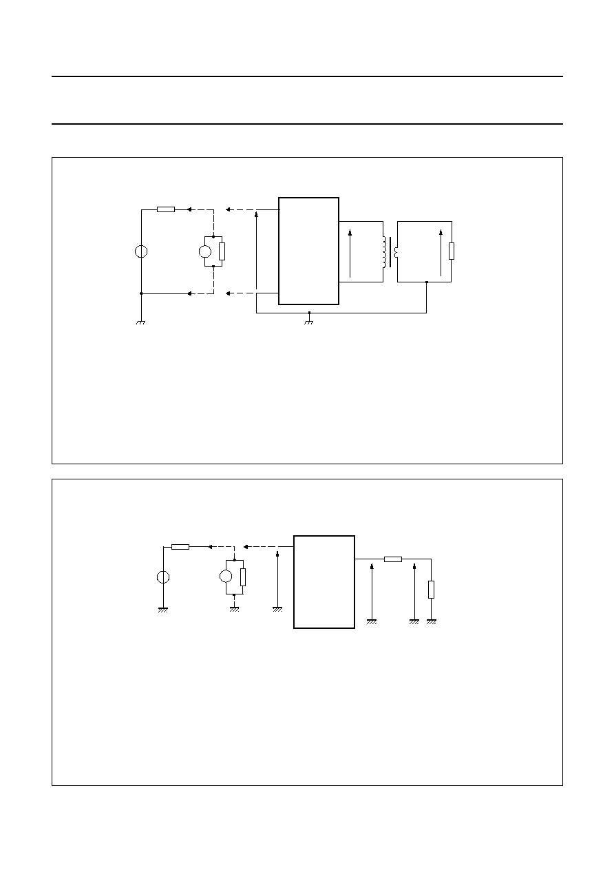
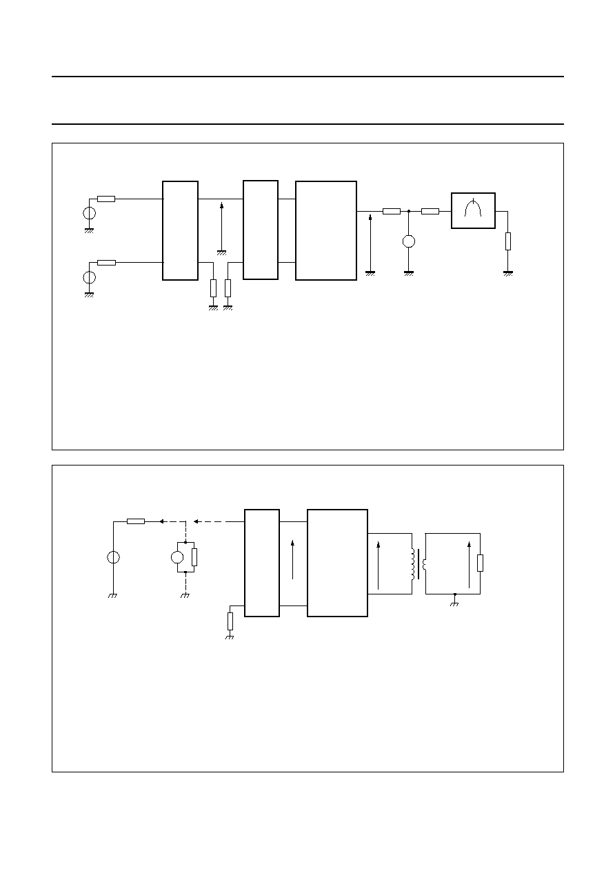
13 TEST AND APPLICATION INFORMATION
mdb265
signal
source
V
V
i(meas)
D.U.T.
LOW_RFIN
GND
IFAMP_OUT1
IFAMP_OUT2
e
50
50
50
V
i
V
o
V
o(meas)
2 x 5
turns
2
turns
RMS
voltmeter
spectrum
analyzer
N1/N2 = 5
Fig.10 Gain measurement in the LOW-band of the TDA6508; TDA6509.
Z
i
>> 50
V
i
= 2
◊
V
i(meas)
= 80 dB
µ
V.
V
i
= V
i(meas)
+ 6 dB = 80 dB
µ
V.
V
o
= V
o(meas)
+ 15 dB (transformer ratio N1/N2 and transformer loss).
G
v
= 20 log
PAL f
IF
= 36.15 MHz.
V
o
V
i
------
handbook, full pagewidth
MDB266
50
27
50
50
V
LOW_RFIN
IFAMP_OUT1
e
Vi(meas)
RMS
voltmeter
spectrum
analyzer
Vo
Vo(meas)
Vi
D.U.T.
signal
source
Fig.11 Gain measurement in the LOW-band of the TDA6508A; TDA6509A.
Z
i
>> 50
V
i
= 2
◊
V
i(meas)
= 80 dB
µ
V.
V
i
= V
i(meas)
+ 6 dB = 80 dB
µ
V.
V
o
= V
o(meas)
+ 3.75 dB.
G
v
= 20 log
PAL f
IF
= 36.15 MHz.
V
o
V
i
------

2005 Mar 25
23
Philips Semiconductors
Product specification
3-band mixer/oscillator and PLL for
terrestrial tuners
TDA6508; TDA6508A;
TDA6509; TDA6509A
handbook, full pagewidth
FCE578
L1
C2
C1
PCB
plug
plug
BNC
BNC
RIM-RIM
I1
C4
C3
PCB
RIM-RIM
I3
I2
(a)
(b)
Fig.12 Input circuit for optimum noise figure in LOW and MID-bands.
(a) f
RF
= 50 MHz:
LOW band mixer frequency response measured = 57 MHz, loss = 0 dB.
image suppression = 16 dB.
C1 = 9 pF.
C2 = 15 pF.
L1 = 7 turns (
5.5 mm, wire
= 0.5 mm).
l1 = semi-rigid (RIM) cable, length = 5 cm (33 dB/100 m,
50
and 96 pF/m).
(b) For f
RF
= 150 MHz:
MID band mixer frequency response measured = 150.3 MHz,
loss = 0 dB.
image suppression = 13 dB.
C3 = 5 pF.
C4 = 25 pF.
l2 = semi-rigid (RIM) cable, length = 30 cm.
l3 = semi-rigid (RIM) cable, length = 5 cm (33 dB/100 m,
50
and 96 pF/m).
mdb263
D.U.T.
INPUT
CIRCUIT
LOW_RFIN or
MID_RFIN
GND
IFAMP_OUT1
IFAMP_OUT2
BNC
RIM
NOISE
METER
NOISE
SOURCE
2 x 5
turns
2
turns
N1/N2 = 5
Fig.13 Noise figure measurement in the LOW and MID-bands of the TDA6508; TDA6509.
NF = NF
meas
-
input circuit loss (dB).

2005 Mar 25
24
Philips Semiconductors
Product specification
3-band mixer/oscillator and PLL for
terrestrial tuners
TDA6508; TDA6508A;
TDA6509; TDA6509A
handbook, full pagewidth
MDB264
LOW_RFIN or
MID_RFIN
IFAMP_OUT1
D.U.T.
NOISE
SOURCE
NOISE
FIGURE
METER
BNC
RIM
INPUT
CIRCUIT
27
Fig.14 Noise figure measurement in the LOW and MID-bands of the TDA6508A; TDA6509A.
NF = f
meas
-
input circuit loss (dB).
handbook, full pagewidth
unwanted
signal
source
eu
ew
50
50
wanted
signal
source
50
MDB261
D.U.T.
LOW_RFIN
IFAMP_OUT1
IFAMP_OUT2
18 dB
attenuator
50
o
N1/N2 = 5
2 x 5
turns
2
turns
V
FILTER
38.9 MHz
modulation
analyzer
HYBRID
A
C
B
D
V
RMS
voltmeter
Vi
AM = 30%
Vo(meas)
Fig.15 Cross-modulation measurement in the LOW-band of the TDA6508; TDA6509.
V
o
= V
o(meas)
+ 15 dB (transformer ratio N1/N2 and transformer loss).
Wanted output signal at picture carrier frequency f
RF(w)
; V
o(w)
= 110 dB
µ
V.
Unwanted output signal at sound sub-carrier frequency f
RF(u)
; AM = 30%; AF = 2 kHz.
Measuring the level of unwanted signal causing 0.3% AM in the wanted signal.
f
RF(w)
= 43.25 MHz (min); 161.25 MHz (max).
f
RF(u)
= 48.75 MHz (min); 166.75 MHz (max).
f
osc
= 82.15 MHz (min); 200.15 MHz (max.).

2005 Mar 25
25
Philips Semiconductors
Product specification
3-band mixer/oscillator and PLL for
terrestrial tuners
TDA6508; TDA6508A;
TDA6509; TDA6509A
handbook, full pagewidth
MDB262
50
50
27
50
50
38.9 MHz
V
LOW_RFIN
IFAMP_OUT1
A
B
C
D
HYBRID
ew
eu
18 dB
attenuator
Vo(meas)
RMS
voltmeter
modulation
analyzer
unwanted
signal
source
wanted
signal
source
AM = 30%
Vo
Vi
FILTER
D.U.T.
Fig.16 Cross-modulation measurement in the LOW-band of the TDA6508A; TDA6509A.
V
o
= V
o(meas)
+ 3.75 dB (transformer ratio N1/N2 and transformer loss).
Wanted output signal at picture carrier frequency f
RF(w)
; V
o(w)
= 100 dB
µ
V.
Unwanted output signal at sound sub-carrier frequency f
RF(u)
; AM = 30%; AF = 2 kHz.
Measuring the level of unwanted signal causing 0.3% AM in the wanted signal.
f
RF(w)
= 43.25 MHz (min.); 161.25 MHz (max.).
f
RF(u)
= 48.75 MHz (min.); 166.75 MHz (max.).
f
osc
= 82.15 MHz (min.); 200.15 MHz (max.).
mdb259
D.U.T.
MID_RFIN1
MID_RFIN2
IFAMP_OUT1
IFAMP_OUT2
50
2 x 5
turns
2
turns
V
i
V
o
V
o(meas)
spectrum
analyzer
signal
source
V
HYBRID
A
C
B
D
N1/N2 = 5
e
50
50
50
V
i(meas)
RMS
voltmeter
Fig.17 Gain measurement in the MID-band of the TDA6508; TDA6509.
Z
i
>> 50
, symmetrical input.
Hybrid loss = 1 dB.
V
i
= V
i(meas)
-
loss + 6 + 3 = 80 dB
µ
V.
V
o
= V
o(meas)
+ 15 dB (transformer ratio N1/N2 and transformer loss).
G
v
= 20 log
PAL f
IF
= 36.15 MHz.
V
o
V
i
------

2005 Mar 25
26
Philips Semiconductors
Product specification
3-band mixer/oscillator and PLL for
terrestrial tuners
TDA6508; TDA6508A;
TDA6509; TDA6509A
handbook, full pagewidth
MDB260
MID_RFIN2
Vi
50
27
50
50
V
MID_RFIN1
IFAMP_OUT1
e
Vi(meas)
RMS
voltmeter
spectrum
analyzer
Vo
D.U.T.
Vo(meas)
signal
source
50
A
B
C
D
HYBRID
Fig.18 Gain measurement in the MID-band of the TDA6508A; TDA6509A.
Z
i
>> 50
symmetrical input.
Hybrid loss = 1 dB.
V
i
= V
i(meas)
-
loss + 6 + 3 = 80 dB
µ
V.
V
o
= V
o(meas)
+ 3.75 dB.
G
v
= 20 log
PAL f
IF
= 36.15 MHz.
V
o
V
i
------
handbook, full pagewidth
unwanted
signal
source
50
50
wanted
signal
source
50
50
MDB253
D.U.T.
MID_RFIN1
MID_RFIN2
IFAMP_OUT1
IFAMP_OUT2
18 dB
attenuator
50
o
N1/N2 = 5
2 x 5
turns
2
turns
V
FILTER
38.9 MHz
modulation
analyzer
HYBRID
A
C
B
D
HYBRID
A
C
B
D
V
RMS
voltmeter
Vi
Vo(meas)
AM = 30%
eu
ew
Fig.19 Cross-modulation measurement in the MID-band of the TDA6508; TDA6509.
V
o
= V
o(meas)
+ 15 dB (transformer ratio N1/N2 and transformer loss).
Wanted output signal at picture carrier frequency f
RF(w)
; V
o(w)
= 110 dB
µ
V.
Unwanted output signal at sound sub-carrier frequency f
RF(u)
; AM = 30%; AF = 2 kHz.
Measuring the level of unwanted signal causing 0.3% AM in the wanted signal.
f
RF(w)
= 154.25 MHz (min.); 447.25 MHz (max.).
f
RF(u)
= 159.75 MHz (min.); 452.75 MHz (max.).
f
osc
= 193.15 MHz (min.); 486.15 MHz (max.).
2005 Mar 25
27
Philips Semiconductors
Product specification
3-band mixer/oscillator and PLL for
terrestrial tuners
TDA6508; TDA6508A;
TDA6509; TDA6509A
handbook, full pagewidth
50
50
50
50
ew
eu
unwanted
signal
source
wanted
signal
source
AM = 30%
Vi
MDB254
27
50
38.9 MHz
V
MID_RFIN1
MID_RFIN2
IFAMP_OUT1
A
B
C
D
HYBRID
A
B
C
D
HYBRID
18 dB
attenuator
Vo(meas)
RMS
voltmeter
modulation
analyzer
Vo
FILTER
D.U.T.
Fig.20 Cross-modulation measurement in the MID-band of the TDA6508A; TDA6509A.
V
o
= V
o(meas)
+ 3.75 dB.
Wanted output signal at fpix; V
o(w)
= 100 dB
µ
V.
Unwanted output signal at fsnd; AM = 30%; AF = 2 kHz.
Measuring the level of unwanted signal causing 0.3% AM in the wanted signal.
f
RF(w)
= 154.25 MHz (min.); 447.25 MHz (max.).
f
RF(u)
= 159.75 MHz (min.); 452.75 MHz (max.).
f
osc
= 193.15 MHz (min.); 486.15 MHz (max.).
mdb257
D.U.T.
HIGH_RFIN1
HIGH_RFIN2
IFAMP_OUT1
IFAMP_OUT2
50
2 x 5
turns
2
turns
V
i
V
o
V
o(meas)
spectrum
analyzer
signal
source
V
HYBRID
A
C
B
D
N1/N2 = 5
e
50
50
50
V
i(meas)
RMS
voltmeter
Fig.21 Gain measurement in the HIGH-band of the TDA6508; TDA6509.
Hybrid loss = 1 dB.
V
i
= V
i(meas)
-
loss = 70 dB
µ
V.
V
o
= V
o(meas)
+ 15 dB (transformer ratio N1/N2 and transformer loss).
G
v
= 20 log
PAL f
IF
= 36.15 MHz.
V
o
V
i
------

2005 Mar 25
28
Philips Semiconductors
Product specification
3-band mixer/oscillator and PLL for
terrestrial tuners
TDA6508; TDA6508A;
TDA6509; TDA6509A
handbook, full pagewidth
MDB258
HIGH_RFIN2
Vi
50
27
50
50
V
HIGH_RFIN1
IFAMP_OUT1
e
Vi(meas)
RMS
voltmeter
spectrum
analyzer
Vo
D.U.T.
Vo(meas)
signal
source
50
A
B
C
D
HYBRID
Fig.22 Gain measurement in the HIGH-band of the TDA6508A; TDA6509A.
Hybrid loss = 1 dB.
V
i
= V
i(meas)
-
loss = 70 dB
µ
V.
V
o
= V
o(meas)
+ 3.75 dB.
G
v
= 20 log
PAL f
IF
= 36.15 MHz.
V
o
V
i
------
mdb255
D.U.T.
IFAMP_OUT1
IFAMP_OUT2
NOISE
METER
NOISE
SOURCE
2 x 5
turns
2
turns
N1/N2 = 5
HYBRID
A
C
B
D
50
HIGH_RFIN1
HIGH_RFIN2
Fig.23 Noise figure measurement in the HIGH-band of the TDA6508; TDA6509.
Hybrid loss = 1 dB.
NF = NF
meas
-
hybrid loss.

2005 Mar 25
29
Philips Semiconductors
Product specification
3-band mixer/oscillator and PLL for
terrestrial tuners
TDA6508; TDA6508A;
TDA6509; TDA6509A
handbook, full pagewidth
MDB256
27
HIGH_RFIN1
HIGH_RFIN2
IFAMP_OUT1
D.U.T.
NOISE
SOURCE
NOISE
FIGURE
METER
50
A
B
C
D
HYBRID
Fig.24 Noise figure measurement in the HIGH-band of the TDA6508A; 6509A.
Hybrid loss = 1 dB.
NF = NF
meas
-
hybrid loss.
handbook, full pagewidth
unwanted
signal
source
50
50
wanted
signal
source
50
50
MDB251
D.U.T.
HIGH_RFIN1
HIGH_RFIN2
IFAMP_OUT1
IFAMP_OUT2
18 dB
attenuator
50
o
N1/N2 = 5
2 x 5
turns
2
turns
V
FILTER
38.9 MHz
modulation
analyzer
HYBRID
A
C
B
D
HYBRID
A
C
B
D
V
RMS
voltmeter
Vi
Vo(meas)
AM = 30%
eu
ew
Fig.25 Cross-modulation measurement in the HIGH-band of the TDA6508; TDA6509.
V
o
= V
o(meas)
+ 15 dB (transformer ratio N1/N2 and transformer loss).
Wanted output signal at picture carrier frequency f
RF(w)
; V
o(w)
= 110 dB
µ
V.
Unwanted output signal at sound sub-carrier frequency f
RF(u)
; AM = 30%; AF = 2 kHz.
Measuring the level of unwanted signal causing 0.3% AM in the wanted signal.
f
RF(w)
= 439.25 MHz (min.); 863.25 MHz (max.).
f
RF(u)
= 444.75 MHz (min.); 868.75 MHz (max.).
f
osc
= 478.15 MHz (min.); 902.15 MHz (max.).

2005 Mar 25
30
Philips Semiconductors
Product specification
3-band mixer/oscillator and PLL for
terrestrial tuners
TDA6508; TDA6508A;
TDA6509; TDA6509A
handbook, full pagewidth
50
50
50
50
ew
eu
unwanted
signal
source
wanted
signal
source
AM = 30%
Vi
MDB252
27
50
38.9 MHz
V
HIGH_RFIN1
HIGH_RFIN2
IFAMP_OUT1
A
B
C
D
HYBRID
A
B
C
D
HYBRID
18 dB
attenuator
Vo(meas)
RMS
voltmeter
modulation
analyzer
Vo
FILTER
D.U.T.
Fig.26 Cross-modulation measurement in the HIGH-band of the TDA6508A; TDA6509A.
V
o
= V
o(meas)
+ 3.75 dB.
Wanted output signal at picture carrier frequency f
RF(w)
; V
o(w)
= 100 dB
µ
V.
Unwanted output signal at sound sub-carrier frequency f
RF(u)
; AM = 30%; AF = 2 kHz.
We measure the level of unwanted signal causing 0.3% AM modulation in the wanted signal
f
RF(w)
= 439.25 MHz (min.); 863.25 MHz (max.).
f
RF(u)
= 444.75 MHz (min.); 868.75 MHz (max.).
f
osc
= 478.15 MHz (min.); 902.15 MHz (max.).

2005
Mar
25
31
Philips Semiconductors
Product specification
3-band mix
er/oscillator and PLL f
o
r
terrestr
ial tuners
TD
A6508; TD
A6508A;
TD
A6509; TD
A6509A
This text is here in white to force landscape pages to be rotated correctly when browsing through the pdf in the Acrobat reader.This text is here in
_
white to force landscape pages to be rotated correctly when browsing through the pdf in the Acrobat reader.This text is here inThis text is here in
white to force landscape pages to be rotated correctly when browsing through the pdf in the Acrobat reader. white to force landscape pages to be ...
13.1
Measurement cir
cuit
mdb249
HIGH_RFIN1
HIGH_RFIN2
MID_RFIN1
MID_RFIN2
LOW_RFIN
RF_GND
MIX_OUT1
MIX_OUT2
IFAMP_IN1
IFAMP_IN2
P1
P0
VT
CP
ADC/P4
AS
AS
PLL_GND
IFAMP_OUT1
IFAMP_OUT2/IF_GND
P3
SDA
SCL
P2
(1) 32
(2) 31
(3) 30
(4) 29
(5) 28
(6) 27
(7) 26
(8) 25
(9) 24
(10) 23
(12) 21
(13) 20
(14) 19
(15) 18
(16) 17
(11) 22
1 (32)
2 (31)
3 (30)
4 (29)
5 (28)
6 (27)
7 (26)
8 (25)
9 (24)
10 (23)
12 (21)
13 (20)
14 (19)
15 (18)
16 (17)
11 (22)
TDA6508
TDA6508A
(TDA6509)
(TDA6509A)
XTAL_REF
HIGH_OSCIN2
HIGH_OSCIN1
MID_OSCIN2
LOW_OSCOUT
OSC_GND
LOW_OSCIN
MID_OSCIN1
VCC
L1
C15
4.7 nF
LOW_RFIN
MID_RFIN2
MID_RFIN1
HIGH_RFIN2
HIGH_RFIN1
C27
4.7 nF
C13
4.7 nF
C12
18 pF
C11
18 pF
R16
1 k
R13
1 k
+
5 V
R14
1 k
R15
1 k
R17
330
R18
330
J1
R8
4.7 k
R9
4.7 k
C1
10 uF
(50 V)
J11
TEST
C9
4.7 nF
C21
4.7 nF
C22
4.7 nF
C29
100 pF
C28
100 pF
R27
33
L2
L3
L4
C4
82 pF
C32
100 pF
C33
100 pF
C34
39 pF
C35
C10
4.7 nF
C26
12 pF
C16
4.7 nF
C31
4.7 nF
R19
27
R11
R1
33 k
VCC
30 V
C3
10 uF
(50 V)
C2
10 uF
(50 V)
C23
18 pF
Y1
4 MHz
J12
1 k
C8
6.8 nF
C17
C7
68 nF
R2
39 k
C18
2.2 nF
39 pF
R20
10
R5
5.6 k
R3
5.6 k
R4
5.6 k
R6
5.6 k
R7
5.6 k
C5
1.8 pF
C6
1 pF
R26
12
1
2
3
4
5
6
J2
1
2
3
4
D1
1
2
3
4
6
Vtune
Vtune
Vtune
Vtune
VCC
IFAMP_OUT
for test purposes only
IFAMP_OUT1
+
5 V
XTAL_REF
ADC
R12
1 k
J3
J4
J5
J7
J6
D5
D2
D3
D4
J8
J9
D6
BB187
D8
BB187
D7
BB179
Fig.27 Measurement circuit for TDA6508; TDA6509; TDA6508A; TDA6509A: PAL application.
The pin numbers in parenthesis refer to the TDA6509 and TDA6509A.

2005 Mar 25
32
Philips Semiconductors
Product specification
3-band mixer/oscillator and PLL for
terrestrial tuners
TDA6508; TDA6508A;
TDA6509; TDA6509A
14 INTERNAL PIN CONFIGURATION
SYMBOL
PIN
DESCRIPTION
(1)
AVERAGE DC VOLTAGE (V)
TDA6508 TDA6509
LOW
MID
HIGH
HIGH_RFIN1,
HIGH_RFIN2
1, 2
32, 31
-
-
1.0
MID_RFIN1,
MID_RFIN2
3, 4
30, 29
-
1.0
-
LOW_RFIN
5
28
1.8
-
-
RF_GND
6
27
-
-
-
MIX_OUT1,
MIX_OUT2
7, 8
26, 25
2.9
2.9
2.9
MDB228
1
2
(31)
(32)
MDB229
3
(30)
4
(29)
MDB230
5
(28)
MDB231
6
(27)
MDB232
7
(26)
8
(25)

2005 Mar 25
33
Philips Semiconductors
Product specification
3-band mixer/oscillator and PLL for
terrestrial tuners
TDA6508; TDA6508A;
TDA6509; TDA6509A
IFAMP_IN1,
IFAMP_IN2
9, 10
24, 23
3.0
3.0
3.0
P0, P1, P2, P3
13, 12,
11, 14
20, 21,
22, 19
high-Z
or
V
CC
-
V
DS
high-Z
or
V
CC
-
V
DS
high-Z
or
V
CC
-
V
DS
SDA
15
18
high-Z
high-Z
high-Z
SCL
16
17
high-Z
high-Z
high-Z
XTAL_REF
17
16
1.6
1.6
1.6
SYMBOL
PIN
DESCRIPTION
(1)
AVERAGE DC VOLTAGE (V)
TDA6508 TDA6509
LOW
MID
HIGH
MDB241
9
(24)
10
(23)
MDB242
11
(22)
12
(21)
13
(20)
14
(19)
15
(18)
MDB244
MDB243
16
(17)
MDB245
17
(16)

2005 Mar 25
34
Philips Semiconductors
Product specification
3-band mixer/oscillator and PLL for
terrestrial tuners
TDA6508; TDA6508A;
TDA6509; TDA6509A
ADC/P4
18
15
high-Z or
V
CC
-
V
DS
high-Z or
V
CC
-
V
DS
high-Z or
V
CC
-
V
DS
CP
19
14
1.0
1.0
1.0
VT
20
13
V
VT
V
VT
V
VT
AS
21
12
1.25
1.25
1.25
PLL_GND
22
11
0
0
0
SYMBOL
PIN
DESCRIPTION
(1)
AVERAGE DC VOLTAGE (V)
TDA6508 TDA6509
LOW
MID
HIGH
MDB246
18
(15)
19
(14)
MDB247
20
MDB248
(13)
MDB236
21
(12)
MDB237
22
(11)

2005 Mar 25
35
Philips Semiconductors
Product specification
3-band mixer/oscillator and PLL for
terrestrial tuners
TDA6508; TDA6508A;
TDA6509; TDA6509A
IFAMP_OUT1,
IFAMP_OUT2
23, 24
10, 9
2.0
2.0
2.0
IF_GND
24
9
0
0
0
V
CC
25
8
supply voltage
5
5
5
HIGH_OSCIN1
26, 27
7, 6
2.3
2.3
1.3
SYMBOL
PIN
DESCRIPTION
(1)
AVERAGE DC VOLTAGE (V)
TDA6508 TDA6509
LOW
MID
HIGH
MDB233
23
(10)
24
(9)
MDB238
24
(9)
MDB239
26
(7)
27
(6)
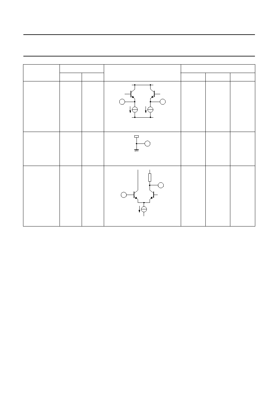
2005 Mar 25
36
Philips Semiconductors
Product specification
3-band mixer/oscillator and PLL for
terrestrial tuners
TDA6508; TDA6508A;
TDA6509; TDA6509A
Note
1. The pin numbers in parenthesis apply to the TDA6508TT.
MID_OSCIN1
28, 29
5, 4
2.3
1.3
2.3
OSC_GND
30
3
0
0
0
LOW_OSCOUT,
LOW_OSCIN
31, 32
2, 1
1.7, 2.9
1.4, 3.5
1.4, 3.5
SYMBOL
PIN
DESCRIPTION
(1)
AVERAGE DC VOLTAGE (V)
TDA6508 TDA6509
LOW
MID
HIGH
MDB240
28
(5)
29
(4)
MDB234
30
(3)
MDB235
32
31
(1)
(2)

2005 Mar 25
37
Philips Semiconductors
Product specification
3-band mixer/oscillator and PLL for
terrestrial tuners
TDA6508; TDA6508A;
TDA6509; TDA6509A
15 PACKAGE OUTLINES
UNIT
A1
A2
A3
bp
c
D
(1)
E
(2)
e
HE
L
Lp
Z
y
w
v
REFERENCES
OUTLINE
VERSION
EUROPEAN
PROJECTION
ISSUE DATE
IEC
JEDEC
JEITA
mm
0.15
0.05
0.95
0.85
0.30
0.19
0.20
0.09
11.1
10.9
6.2
6.0
0.65
8.3
7.9
0.78
0.48
8
0
o
o
0.1
0.1
0.2
1
DIMENSIONS (mm are the original dimensions)
Notes
1. Plastic or metal protrusions of 0.15 mm maximum per side are not included.
2. Plastic interlead protrusions of 0.25 mm maximum per side are not included.
0.75
0.50
SOT487-1
MO-153
99-12-27
03-02-18
w
M
bp
D
Z
e
0.25
1
16
32
17
A
A
1
A
2
Lp
detail X
L
(A )
3
H
E
E
c
v
M
A
X
A
y
0
2.5
5 mm
scale
TSSOP32: plastic thin shrink small outline package; 32 leads; body width 6.1 mm;
lead pitch 0.65 mm
SOT487-1
A
max.
1.1
pin 1 index

2005 Mar 25
38
Philips Semiconductors
Product specification
3-band mixer/oscillator and PLL for
terrestrial tuners
TDA6508; TDA6508A;
TDA6509; TDA6509A
0.5
1
A1
Eh
b
UNIT
y
e
0.2
c
REFERENCES
OUTLINE
VERSION
EUROPEAN
PROJECTION
ISSUE DATE
IEC
JEDEC
JEITA
mm
5.1
4.9
Dh
3.25
2.95
y1
5.1
4.9
3.25
2.95
e1
3.5
e2
3.5
0.30
0.18
0.05
0.00
0.05
0.1
DIMENSIONS (mm are the original dimensions)
SOT617-1
MO-220
- - -
- - -
0.5
0.3
L
0.1
v
0.05
w
0
2.5
5 mm
scale
SOT617-1
HVQFN32: plastic thermal enhanced very thin quad flat package; no leads;
32 terminals; body 5 x 5 x 0.85 mm
A
(1)
max.
A
A1
c
detail X
y
y1 C
e
L
Eh
Dh
e
e1
b
9
16
32
25
24
17
8
1
X
D
E
C
B
A
e2
terminal 1
index area
terminal 1
index area
01-08-08
02-10-18
1/2
e
1/2
e
A
C
C
B
v
M
w
M
E
(1)
Note
1. Plastic or metal protrusions of 0.075 mm maximum per side are not included.
D
(1)

2005 Mar 25
39
Philips Semiconductors
Product specification
3-band mixer/oscillator and PLL for
terrestrial tuners
TDA6508; TDA6508A;
TDA6509; TDA6509A
16 SOLDERING
16.1
Introduction to soldering surface mount
packages
This text gives a very brief insight to a complex technology.
A more in-depth account of soldering ICs can be found in
our
"Data Handbook IC26; Integrated Circuit Packages"
(document order number 9398 652 90011).
There is no soldering method that is ideal for all surface
mount IC packages. Wave soldering can still be used for
certain surface mount ICs, but it is not suitable for fine pitch
SMDs. In these situations reflow soldering is
recommended.
16.2
Reflow soldering
Reflow soldering requires solder paste (a suspension of
fine solder particles, flux and binding agent) to be applied
to the printed-circuit board by screen printing, stencilling or
pressure-syringe dispensing before package placement.
Driven by legislation and environmental forces the
worldwide use of lead-free solder pastes is increasing.
Several methods exist for reflowing; for example,
convection or convection/infrared heating in a conveyor
type oven. Throughput times (preheating, soldering and
cooling) vary between 100 seconds and 200 seconds
depending on heating method.
Typical reflow peak temperatures range from
215
∞
C to 270
∞
C depending on solder paste material. The
top-surface temperature of the packages should
preferably be kept:
∑
below 225
∞
C (SnPb process) or below 245
∞
C (Pb-free
process)
≠ for all BGA, HTSSON..T and SSOP..T packages
≠ for packages with a thickness
2.5 mm
≠ for packages with a thickness < 2.5 mm and a
volume
350 mm
3
so called thick/large packages.
∑
below 240
∞
C (SnPb process) or below 260
∞
C (Pb-free
process) for packages with a thickness < 2.5 mm and a
volume < 350 mm
3
so called small/thin packages.
Moisture sensitivity precautions, as indicated on packing,
must be respected at all times.
16.3
Wave soldering
Conventional single wave soldering is not recommended
for surface mount devices (SMDs) or printed-circuit boards
with a high component density, as solder bridging and
non-wetting can present major problems.
To overcome these problems the double-wave soldering
method was specifically developed.
If wave soldering is used the following conditions must be
observed for optimal results:
∑
Use a double-wave soldering method comprising a
turbulent wave with high upward pressure followed by a
smooth laminar wave.
∑
For packages with leads on two sides and a pitch (e):
≠ larger than or equal to 1.27 mm, the footprint
longitudinal axis is preferred to be parallel to the
transport direction of the printed-circuit board;
≠ smaller than 1.27 mm, the footprint longitudinal axis
must be parallel to the transport direction of the
printed-circuit board.
The footprint must incorporate solder thieves at the
downstream end.
∑
For packages with leads on four sides, the footprint must
be placed at a 45
∞
angle to the transport direction of the
printed-circuit board. The footprint must incorporate
solder thieves downstream and at the side corners.
During placement and before soldering, the package must
be fixed with a droplet of adhesive. The adhesive can be
applied by screen printing, pin transfer or syringe
dispensing. The package can be soldered after the
adhesive is cured.
Typical dwell time of the leads in the wave ranges from
3 seconds to 4 seconds at 250
∞
C or 265
∞
C, depending
on solder material applied, SnPb or Pb-free respectively.
A mildly-activated flux will eliminate the need for removal
of corrosive residues in most applications.
16.4
Manual soldering
Fix the component by first soldering two
diagonally-opposite end leads. Use a low voltage (24 V or
less) soldering iron applied to the flat part of the lead.
Contact time must be limited to 10 seconds at up to
300
∞
C.
When using a dedicated tool, all other leads can be
soldered in one operation within 2 seconds to 5 seconds
between 270
∞
C and 320
∞
C.

2005 Mar 25
40
Philips Semiconductors
Product specification
3-band mixer/oscillator and PLL for
terrestrial tuners
TDA6508; TDA6508A;
TDA6509; TDA6509A
16.5
Suitability of surface mount IC packages for wave and reflow soldering methods
Notes
1. For more detailed information on the BGA packages refer to the
"(LF)BGA Application Note" (AN01026); order a copy
from your Philips Semiconductors sales office.
2. All surface mount (SMD) packages are moisture sensitive. Depending upon the moisture content, the maximum
temperature (with respect to time) and body size of the package, there is a risk that internal or external package
cracks may occur due to vaporization of the moisture in them (the so called popcorn effect). For details, refer to the
Drypack information in the
"Data Handbook IC26; Integrated Circuit Packages; Section: Packing Methods".
3. These transparent plastic packages are extremely sensitive to reflow soldering conditions and must on no account
be processed through more than one soldering cycle or subjected to infrared reflow soldering with peak temperature
exceeding 217
∞
C
±
10
∞
C measured in the atmosphere of the reflow oven. The package body peak temperature
must be kept as low as possible.
4. These packages are not suitable for wave soldering. On versions with the heatsink on the bottom side, the solder
cannot penetrate between the printed-circuit board and the heatsink. On versions with the heatsink on the top side,
the solder might be deposited on the heatsink surface.
5. If wave soldering is considered, then the package must be placed at a 45
∞
angle to the solder wave direction.
The package footprint must incorporate solder thieves downstream and at the side corners.
6. Wave soldering is suitable for LQFP, QFP and TQFP packages with a pitch (e) larger than 0.8 mm; it is definitely not
suitable for packages with a pitch (e) equal to or smaller than 0.65 mm.
7. Wave soldering is suitable for SSOP, TSSOP, VSO and VSSOP packages with a pitch (e) equal to or larger than
0.65 mm; it is definitely not suitable for packages with a pitch (e) equal to or smaller than 0.5 mm.
8. Image sensor packages in principle should not be soldered. They are mounted in sockets or delivered pre-mounted
on flex foil. However, the image sensor package can be mounted by the client on a flex foil by using a hot bar
soldering process. The appropriate soldering profile can be provided on request.
9. Hot bar soldering or manual soldering is suitable for PMFP packages.
PACKAGE
(1)
SOLDERING METHOD
WAVE
REFLOW
(2)
BGA, HTSSON..T
(3)
, LBGA, LFBGA, SQFP, SSOP..T
(3)
, TFBGA,
VFBGA, XSON
not suitable
suitable
DHVQFN, HBCC, HBGA, HLQFP, HSO, HSOP, HSQFP, HSSON,
HTQFP, HTSSOP, HVQFN, HVSON, SMS
not suitable
(4)
suitable
PLCC
(5)
, SO, SOJ
suitable
suitable
LQFP, QFP, TQFP
not recommended
(5)(6)
suitable
SSOP, TSSOP, VSO, VSSOP
not recommended
(7)
suitable
CWQCCN..L
(8)
, PMFP
(9)
, WQCCN..L
(8)
not suitable
not suitable

2005 Mar 25
41
Philips Semiconductors
Product specification
3-band mixer/oscillator and PLL for
terrestrial tuners
TDA6508; TDA6508A;
TDA6509; TDA6509A
17 DATA SHEET STATUS
Notes
1. Please consult the most recently issued data sheet before initiating or completing a design.
2. The product status of the device(s) described in this data sheet may have changed since this data sheet was
published. The latest information is available on the Internet at URL http://www.semiconductors.philips.com.
3. For data sheets describing multiple type numbers, the highest-level product status determines the data sheet status.
LEVEL
DATA SHEET
STATUS
(1)
PRODUCT
STATUS
(2)(3)
DEFINITION
I
Objective data
Development
This data sheet contains data from the objective specification for product
development. Philips Semiconductors reserves the right to change the
specification in any manner without notice.
II
Preliminary data Qualification
This data sheet contains data from the preliminary specification.
Supplementary data will be published at a later date. Philips
Semiconductors reserves the right to change the specification without
notice, in order to improve the design and supply the best possible
product.
III
Product data
Production
This data sheet contains data from the product specification. Philips
Semiconductors reserves the right to make changes at any time in order
to improve the design, manufacturing and supply. Relevant changes will
be communicated via a Customer Product/Process Change Notification
(CPCN).
18 DEFINITIONS
Short-form specification
The data in a short-form
specification is extracted from a full data sheet with the
same type number and title. For detailed information see
the relevant data sheet or data handbook.
Limiting values definition
Limiting values given are in
accordance with the Absolute Maximum Rating System
(IEC 60134). Stress above one or more of the limiting
values may cause permanent damage to the device.
These are stress ratings only and operation of the device
at these or at any other conditions above those given in the
Characteristics sections of the specification is not implied.
Exposure to limiting values for extended periods may
affect device reliability.
Application information
Applications that are
described herein for any of these products are for
illustrative purposes only. Philips Semiconductors make
no representation or warranty that such applications will be
suitable for the specified use without further testing or
modification.
19 DISCLAIMERS
Life support applications
These products are not
designed for use in life support appliances, devices, or
systems where malfunction of these products can
reasonably be expected to result in personal injury. Philips
Semiconductors customers using or selling these products
for use in such applications do so at their own risk and
agree to fully indemnify Philips Semiconductors for any
damages resulting from such application.
Right to make changes
Philips Semiconductors
reserves the right to make changes in the products -
including circuits, standard cells, and/or software -
described or contained herein in order to improve design
and/or performance. When the product is in full production
(status `Production'), relevant changes will be
communicated via a Customer Product/Process Change
Notification (CPCN). Philips Semiconductors assumes no
responsibility or liability for the use of any of these
products, conveys no licence or title under any patent,
copyright, or mask work right to these products, and
makes no representations or warranties that these
products are free from patent, copyright, or mask work
right infringement, unless otherwise specified.

© Koninklijke Philips Electronics N.V. 2005
SCA76
All rights are reserved. Reproduction in whole or in part is prohibited without the prior written consent of the copyright owner.
The information presented in this document does not form part of any quotation or contract, is believed to be accurate and reliable and may be changed
without notice. No liability will be accepted by the publisher for any consequence of its use. Publication thereof does not convey nor imply any license
under patent- or other industrial or intellectual property rights.
Philips Semiconductors ≠ a worldwide company
Contact information
For additional information please visit http://www.semiconductors.philips.com.
Fax: +31 40 27 24825
For sales offices addresses send e-mail to: sales.addresses@www.semiconductors.philips.com.
Printed in The Netherlands
R25/03/pp
42
Date of release:
2005 Mar 25
Document order number:
9397 750 14909