
1.
General description
The TDA6650ATT; TDA6651ATT is a programmable 3-band mixer / oscillator and low
phase noise PLL synthesizer intended for pure 3-band tuner concepts applied to hybrid
(digital and analog) terrestrial and cable TV reception.
The device includes three double balanced mixers for low, mid and high bands, three
oscillators for the corresponding bands, a switchable IF amplifier, a wideband AGC
detector and a low noise PLL synthesizer. The frequencies of the three bands are shown
in
Table 1
. Two pins are available between the mixer output and the IF amplifier input to
enable IF filtering for improved signal handling and to improve the adjacent channel
rejection.
[1]
RF input frequency is the frequency of the corresponding picture carrier for analog standard.
[2]
For bandwidth optimization please refer to
Application note CC0306V2.
The IF amplifier is switchable in order to drive both symmetrical and asymmetrical
outputs. When it is used as an asymmetrical amplifier, the IFOUTB pin needs to be
connected to the supply voltage V
CCA
.
Five open-drain PMOS ports are included on the IC. Two of them, BS1 and BS2, are also
dedicated to the selection of the low, mid and high bands. PMOS port BS5 pin is shared
with the ADC.
The AGC detector provides a control that can be used in a tuner to set the gain of the
RF stage. Six AGC take-over points are available by software. Two programmable AGC
time constants are available for search tuning and normal tuner operation.
The local oscillator signal is fed to the fractional-N divider. The divided frequency is
compared to the comparison frequency into the fast phase detector which drives the
charge pump. The loop amplifier is also on-chip, including the high-voltage transistor to
drive directly the 33 V tuning voltage without the need to add an external transistor.
The comparison frequency is obtained from an on-chip crystal oscillator. The crystal
frequency can be output to the XTOUT pin to drive the clock input of a digital
demodulation IC.
TDA6650ATT; TDA6651ATT
5 V mixer/oscillator and low noise PLL synthesizer for hybrid
terrestrial tuner (digital and analog)
Rev. 01 -- 14 December 2004
Product data sheet
Table 1:
Recommended band limits in MHz for ISDBT and NTSC Japan tuners
[1] [2]
Band
RF input
Oscillator
Min
Max
Min
Max
Low
91.25
217.25
150
276
Mid
217.25
463.25
276
522
High
463.25
765.25
522
824

9397 750 14179
� Koninklijke Philips Electronics N.V. 2004. All rights reserved.
Product data sheet
Rev. 01 -- 14 December 2004
2 of 53
Philips Semiconductors
TDA6650ATT; TDA6651ATT
5 V mixer/oscillator and low noise PLL synthesizer
Control data is entered via the I
2
C-bus; six serial bytes are required to address the device,
select the Local Oscillator (LO) frequency, select the step frequency, program the output
ports and set the charge pump current or enable or disable the crystal output buffer, select
the AGC take-over point and time constant and/or select a specific test mode. A status
byte concerning the AGC level detector and the ADC voltage can be read out on the SDA
line during a read operation. During a read operation, the loop `in-lock' flag, the power-on
reset flag and the automatic loop bandwidth control flag are read.
The device has 4 programmable addresses. Each address can be selected by applying a
specific voltage to pin AS, enabling the use of multiple devices in the same system.
The I
2
C-bus is fast mode compatible, except for the timing as described in the functional
description and is compatible with 5 V, 3.3 V and 2.5 V microcontrollers depending on the
voltage applied to pin BVS.
2.
Features
s
Single-chip 5 V mixer / oscillator and low phase noise PLL synthesizer for TV and VCR
tuners, dedicated to hybrid (digital and analog) and pure digital applications for
Japanese standards (NTSC and ISDB-T)
s
Five possible step frequencies to cope with different digital terrestrial TV and
analog TV standards
s
Eight charge pump currents between 40
�
A and 600
�
A to reach the optimum phase
noise performance over the bands
s
I
2
C-bus protocol compatible with 2.5 V, 3.3 V and 5 V microcontrollers:
x
Address + 5 data bytes transmission (I
2
C-bus write mode)
x
Address + 1 status byte (I
2
C-bus read mode)
x
Four independent I
2
C-bus addresses.
s
Five PMOS open-drain ports with 15 mA source capability for band switching and
general purpose; one of these ports is combined with a 5-step ADC
s
Wideband AGC detector for internal tuner AGC:
x
Six programmable take-over points
x
Two programmable time constants
x
AGC flag.
s
In-lock flag
s
Crystal frequency output buffer
s
33 V tuning voltage output
s
Fractional-N programmable divider
s
Balanced mixers with a common emitter input for the low band and for the mid band
(each single input)
s
Balanced mixer with a common base input for the high band (balanced input)
s
2-pin asymmetrical oscillator for the low band
s
2-pin symmetrical oscillator for the mid band
s
4-pin symmetrical oscillator for the high band
s
Switched concept IF amplifier with both asymmetrical and symmetrical outputs to drive
low impedance or SAW filters i.e. 500
/ 40 pF.
9397 750 14179
� Koninklijke Philips Electronics N.V. 2004. All rights reserved.
Product data sheet
Rev. 01 -- 14 December 2004
3 of 53
Philips Semiconductors
TDA6650ATT; TDA6651ATT
5 V mixer/oscillator and low noise PLL synthesizer
3.
Applications
For all applications, the recommendations given in the latest
Application note CC0419
must be used.
3.1 Application summary
s
Digital and analog terrestrial tuners (ISDBT and NTSC Japan)
s
Cable tuners (QAM)
s
Digital TV sets
s
Digital set-top boxes.
4.
Ordering information
Table 2:
Ordering information
Type number
Package
Name
Description
Version
TDA6650ATT
TSSOP38
plastic thin shrink small outline package; 38 leads; body width 4.4 mm; lead
pitch 0.5 mm
SOT510-1
TDA6651ATT

9397 750 14179
� Koninklijke Philips Electronics N.V. 2004. All rights reserved.
Product data sheet
Rev. 01 -- 14 December 2004
4 of 53
Philips Semiconductors
TDA6650ATT; TDA6651ATT
5 V mixer/oscillator and low noise PLL synthesizer
5.
Block diagram
The pin numbers in parenthesis represent the TDA6651ATT.
Fig 1.
Block diagram
FRACTIONAL
DIVIDER
CRYSTAL
OSCILLATOR
POR
SCL
SDA
AS
BVS
15 (24)
XTAL1
VT
HOSCIN2
HOSCOUT2
HOSCOUT1
HOSCIN1
19 (20)
5 (34)
(17) 22
CP
(16) 23
(6) 33
(3) 36
(7) 32
(8) 31
(9) 30
XTAL2
20 (19)
16 (23)
17 (22)
13 (26)
ADC
AGC
I
2
C-BUS
TRANSCEIVER
FRACTIONAL
CALCULATOR
PHASE
COMPARATOR
CHARGE
PUMP
OUTPUT
BUFFER
LOOP
AMP
T0, T1, T2
REFERENCE
DIVIDER
LOCK
DETECTOR
BAND SWITCH
OUTPUT PORTS
FRACTIONAL
SPURIOUS
COMPENSATION
HIGH
OSCILLATOR
HIGH
MIXER
HIGH
INPUT
BS1 . BS2
ADC/
BS5
14
(25)
N[14:0]
R0, R1,
R2
BS5-
BS1
V
CCD
24 (15)
HBIN1
1 (38)
HBIN2
2 (37)
MBIN
3 (36)
LBIN
4 (35)
MOSCIN2
MOSCIN1
(4) 35
(5) 34
XTOUT
(21) 18
BS3
10
(29)
BS1
coa033
12
(27)
BS4
8
(31)
BS2
11
(28)
AL0, AL1, AL2
ATC
AGC
flag
AGC
V
CCA
T0, T1,
T2
CP0, CP1,
CP2
BS1 . BS2
MID
OSCILLATOR
MID
MIXER
MID
INPUT
BS2
BS2
LOSCOUT
LOSCIN
(2) 37
(1) 38
IFGND
(10) 29
(30) 9
LOW
OSCILLATOR
AGC
DETECTOR
IFOUTA
IFFIL1
IFOUTB
IFFIL2
7 (32)
6 (33)
27 (12)
28 (11)
26 (13)
n.c.
21 (18)
IF
AMP
LOW
MIXER
TDA6650ATT
(TDA6651ATT)
LOW
INPUT
BS1
BS1
PLLGND
(14) 25
OSCGND
RFGND

9397 750 14179
� Koninklijke Philips Electronics N.V. 2004. All rights reserved.
Product data sheet
Rev. 01 -- 14 December 2004
5 of 53
Philips Semiconductors
TDA6650ATT; TDA6651ATT
5 V mixer/oscillator and low noise PLL synthesizer
6.
Pinning information
6.1 Pin description
Table 3:
Pin description
Symbol
Pin
Description
TDA6650ATT TDA6651ATT
HBIN1
1
38
high band RF input 1
HBIN2
2
37
high band RF input 2
MBIN
3
36
mid band RF input
LBIN
4
35
low band RF input
RFGND
5
34
RF ground
IFFIL1
6
33
IF filter output 1
IFFIL2
7
32
IF filter output 2
BS4
8
31
PMOS open-drain output port 4 for general
purpose
AGC
9
30
AGC output
BS3
10
29
PMOS open-drain output port 3 for general
purpose
BS2
11
28
PMOS open-drain output port 2 to select the mid
band
BS1
12
27
PMOS open-drain output port 1 to select the low
band
BVS
13
26
bus voltage selection input
ADC/BS5
14
25
ADC input or PMOS open-drain output port 5 for
general purpose
SCL
15
24
I
2
C-bus serial clock input
SDA
16
23
I
2
C-bus serial data input and output
AS
17
22
I
2
C-bus address selection input
XTOUT
18
21
crystal frequency buffer output
XTAL1
19
20
crystal oscillator input 1
XTAL2
20
19
crystal oscillator input 2
n.c.
21
18
not connected
VT
22
17
tuning voltage output
CP
23
16
charge pump output
V
CCD
24
15
supply voltage for the PLL part
PLLGND
25
14
PLL ground
V
CCA
26
13
supply voltage for the analog part
IFOUTB
27
12
IF output B for symmetrical amplifier and
asymmetrical IF amplifier switch input
IFOUTA
28
11
IF output A
IFGND
29
10
IF ground
HOSCIN1
30
9
high band oscillator input 1
HOSCOUT1
31
8
high band oscillator output 1
HOSCOUT2
32
7
high band oscillator output 2

9397 750 14179
� Koninklijke Philips Electronics N.V. 2004. All rights reserved.
Product data sheet
Rev. 01 -- 14 December 2004
6 of 53
Philips Semiconductors
TDA6650ATT; TDA6651ATT
5 V mixer/oscillator and low noise PLL synthesizer
6.2 Pinning
7.
Functional description
7.1 Mixer, oscillator and PLL (MOPLL) functions
Bit BS1 enables the BS1 port, the low band mixer and the low band oscillator. Bit BS2
enables the BS2 port, the mid band mixer and the mid band oscillator. When both BS1
and BS2 bits are logic 0, the high band mixer and the high band oscillator are enabled.
The oscillator signal is applied to the fractional-N programmable divider. The divided
signal f
div
is fed to the phase comparator where it is compared in both phase and
frequency with the comparison frequency f
comp
. This frequency is derived from the signal
present on the crystal oscillator f
xtal
and divided in the reference divider. There is a
fractional calculator on the chip that generates the data for the fractional divider as well as
HOSCIN2
33
6
high band oscillator input 2
MOSCIN1
34
5
mid band oscillator input 1
MOSCIN2
35
4
mid band oscillator input 2
OSCGND
36
3
oscillators ground
LOSCOUT
37
2
low band oscillator output
LOSCIN
38
1
low band oscillator input
Table 3:
Pin description
...continued
Symbol
Pin
Description
TDA6650ATT TDA6651ATT
Fig 2.
Pin configuration TDA6650ATT
Fig 3.
Pin configuration TDA6651ATT
TDA6650ATT
HBIN1
LOSCIN
HBIN2
LOSCOUT
MBIN
OSCGND
LBIN
MOSCIN2
RFGND
MOSCIN1
IFFIL1
HOSCIN2
IFFIL2
HOSCOUT2
BS4
HOSCOUT1
AGC
HOSCIN1
BS3
IFGND
BS2
IFOUTA
BS1
IFOUTB
BVS
V
CCA
ADC/BS5
PLLGND
SCL
V
CCD
SDA
CP
AS
VT
XTOUT
n.c.
XTAL1
XTAL2
001aac086
1
2
3
4
5
6
7
8
9
10
11
12
13
14
15
16
17
18
19
38
37
36
35
34
33
32
31
30
29
28
27
26
25
24
23
22
21
20
TDA6651ATT
LOSCIN
HBIN1
LOSCOUT
HBIN2
OSCGND
MBIN
MOSCIN2
LBIN
MOSCIN1
RFGND
HOSCIN2
IFFIL1
HOSCOUT2
IFFIL2
HOSCOUT1
BS4
HOSCIN1
AGC
IFGND
BS3
IFOUTA
BS2
IFOUTB
BS1
V
CCA
BVS
PLLGND
ADC/BS5
V
CCD
SCL
CP
SDA
VT
AS
n.c.
XTOUT
XTAL2
XTAL1
001aac087
1
2
3
4
5
6
7
8
9
10
11
12
13
14
15
16
17
18
19
38
37
36
35
34
33
32
31
30
29
28
27
26
25
24
23
22
21
20

9397 750 14179
� Koninklijke Philips Electronics N.V. 2004. All rights reserved.
Product data sheet
Rev. 01 -- 14 December 2004
7 of 53
Philips Semiconductors
TDA6650ATT; TDA6651ATT
5 V mixer/oscillator and low noise PLL synthesizer
the reference divider ratio, depending on the step frequency selected. The crystal
oscillator requires a 4 MHz crystal in series with an 18 pF capacitor between pins XTAL1
and XTAL2.
The output of the phase comparator drives the charge pump and the loop amplifier
section. This amplifier has an on-chip high voltage drive transistor. Pin CP is the output of
the charge pump, and pin VT is the pin to drive the tuning voltage to the varicap diodes of
the oscillators and the tracking filters. The loop filter has to be connected between pins CP
and VT. The spurious signals introduced by the fractional divider are automatically
compensated by the spurious compensation block.
It is possible to drive the clock input of a digital demodulation IC from pin XTOUT with the
4 MHz signal from the crystal oscillator. This output is also used to output
1
/
2
f
div
and f
comp
signals in a specific test mode (see
Table 8
). It is possible to switch off this output, which is
recommended when it is not used.
For test and alignment purposes, it is also possible to release the tuning voltage output by
selecting the sinking mode (see
Table 8
), and by applying an external voltage on pin VT.
In addition to the BS1 and BS2 output ports that are used for the band selection, there are
three general purpose ports BS3, BS4 and BS5. All five ports are PMOS open-drain type,
each with 15 mA drive capability. The connection for port BS5 and the ADC input is
combined on one pin. It is not possible to use the ADC if port BS5 is used.
The AGC detector compares the level at the IF amplifier output to a reference level which
is selected from 6 different levels via the I
2
C-bus. The time constant of the AGC can be
selected via the I
2
C-bus to cope with normal operation as well as with search operation.
When the output level on pin AGC is higher than the threshold V
RMH
, then bit AGC = 1.
When the output level on pin AGC is lower than the threshold V
RML
, then bit AGC = 0.
Between these two thresholds, bit AGC is not defined. The status of the AGC bit can be
read via the I
2
C-bus according to the read mode as described in
Table 12
.
7.2 I
2
C-bus voltage
The I
2
C-bus lines SCL and SDA can be connected to an I
2
C-bus system tied to 2.5 V,
3.3 V or 5 V. The choice of the bus input threshold voltages is made with pin BVS that can
be left open-circuit, connected to the supply voltage or to ground (see
Table 4
).
7.3 Phase noise, I
2
C-bus traffic and crosstalk
While the TDA6650ATT; TDA6651ATT is dedicated for hybrid terrestrial applications, the
low noise PLL will clean up the noise spectrum of the VCOs close to the carrier to reach
noise levels at 1 kHz offset from the carrier compatible with e.g. ISDB-T reception.
Table 4:
I
2
C-bus voltage selection
Pin BVS connection
Bus voltage
Logic level
LOW
HIGH
To ground
2.5 V
0 V to 0.75 V
1.75 V to 5.5 V
Open-circuit
3.3 V
0 V to 1.0 V
2.3 V to 5.5 V
To V
CC
5 V
0 V to 1.5 V
3.0 V to 5.5 V

9397 750 14179
� Koninklijke Philips Electronics N.V. 2004. All rights reserved.
Product data sheet
Rev. 01 -- 14 December 2004
8 of 53
Philips Semiconductors
TDA6650ATT; TDA6651ATT
5 V mixer/oscillator and low noise PLL synthesizer
Linked to this noise improvement, some disturbances may become visible while they were
not visible because they were hidden into the noise in analog dedicated applications and
circuits.
This is especially true for disturbances coming from the I
2
C-bus traffic, whatever this traffic
is intended for the MOPLL or for another slave on the bus.
To avoid this I
2
C-bus crosstalk and be able to have a clean noise spectrum, it is necessary
to use a bus gate that enables the signal on the bus to drive the MOPLL only when the
communication is intended for the tuner part (such a kind of I
2
C-bus gate is included into
the Philips terrestrial channel decoders), and to avoid unnecessary repeated sending of
the same information.
8.
I
2
C-bus protocol
The TDA6650ATT; TDA6651ATT is controlled via the two-wire I
2
C-bus. For programming,
there is one device address (7 bits) and the R/W bit for selecting read or write mode. To be
able to have more than one MOPLL in an I
2
C-bus system, one of four possible addresses
is selected depending on the voltage applied to address selection pin AS (see
Table 7
).
The TDA6650ATT; TDA6651ATT fulfils the fast mode I
2
C-bus, according to the Philips
I
2
C-bus specification (see
Section 21
), except for the timing as described in
Figure 4
. The
I
2
C-bus interface is designed in such a way that the pins SCL and SDA can be connected
to 5 V, 3.3 V or to 2.5 V pulled-up I
2
C-bus lines, depending on the voltage applied to
pin BVS (see
Table 4
).
8.1 Write mode; R/W = 0
After the address transmission (first byte), data bytes can be sent to the device (see
Table 5
). Five data bytes are needed to fully program the TDA6650ATT; TDA6651ATT.
The I
2
C-bus transceiver has an auto-increment facility that permits programming the
device within one single transmission (address + 5 data bytes).
The TDA6650ATT; TDA6651ATT can also be partly programmed on the condition that the
first data byte following the address is byte 2 (divider byte 1) or byte 4 (control byte 1). The
first bit of the first data byte transmitted indicates whether byte 2 (first bit = 0) or byte 4
(first bit = 1) will follow. Until an I
2
C-bus STOP condition is sent by the controller, additional
data bytes can be entered without the need to re-address the device. The fractional
calculator is updated only at the end of the transmission (STOP condition). Each control
byte is loaded after the 8th clock pulse of the corresponding control byte. Main divider
data are valid only if no new I
2
C-bus transmission is started (START condition) during the
computation period of 50
�
s.
Both DB1 and DB2 need to be sent to change the main divider ratio. If the value of the
ratio selection bits R2, R1 and R0 are changed, the bytes DB1 and DB2 have to be sent in
the same transmission.
9397 750 14179
� Koninklijke Philips Electronics N.V. 2004. All rights reserved.
Product data sheet
Rev. 01 -- 14 December 2004
9 of 53
Philips Semiconductors
TDA6650ATT; TDA6651ATT
5 V mixer/oscillator and low noise PLL synthesizer
[1]
MSB is transmitted first.
Fig 4.
Example of I
2
C-bus transmission frame
ADDRESS
BYTE
DIVIDER
BYTE 1
START
ADDRESS
BYTE
I
2
C-bus transmission
dedicated to
another IC
I
2
C-bus transmission dedicated to
the MOPLL
START
50
�
s
DIVIDER
BYTE 2
CONTROL
BYTE 1
CONTROL
BYTE 2
CONTROL
BYTE 1
CONTROL
BYTE 2
STOP
fce921
Table 5:
I
2
C-bus write data format
Name
Byte
Bit
Ack
MSB
[1]
LSB
Address byte
1
1
1
0
0
0
MA1
MA0
R/W = 0 A
Divider byte 1 (DB1)
2
0
N14
N13
N12
N11
N10
N9
N8
A
Divider byte 2 (DB2)
3
N7
N6
N5
N4
N3
N2
N1
N0
A
Control byte 1 (CB1);
see
Table 6
4
1
T/A = 1
T2
T1
T0
R2
R1
R0
A
1
T/A = 0
0
0
ATC
AL2
AL1
AL0
A
Control byte 2 (CB2)
5
CP2
CP1
CP0
BS5
BS4
BS3
BS2
BS1
A
Table 6:
Description of write data format bits
Bit
Description
A
acknowledge
MA1 and MA0
programmable address bits; see
Table 7
R/W
logic 0 for write mode
N14 to N0
programmable LO frequency;
N = N14
�
2
14
+ N13
�
2
13
+ N12
�
2
12
+ ... + N1
�
2
1
+ N0
T/A
test/AGC bit
T/A = 0: the next 6 bits sent are AGC settings
T/A = 1: the next 6 bits sent are test and reference divider ratio settings
T2, T1 and T0
test bits; see
Table 8
R2, R1, and R0
reference divider ratio and programmable frequency step; see
Table 9
ATC
AGC current setting and time constant; capacitor on pin AGC = 150 nF
ATC = 0: AGC current = 220 nA; AGC time constant = 2 s
ATC = 1: AGC current = 9
�
A; AGC time constant = 50 ms
AL2, AL1 and AL0
AGC take-over point bits; see
Table 10
CP2, CP1 and CP0
charge pump current; see
Table 11
BS5, BS4, BS3, BS2
and BS1
PMOS ports control bits
BSn = 0: corresponding port is off, high-impedance state (status at
power-on reset)
BSn = 1: corresponding port is on; V
O
= V
CC
-
V
DS(sat)

9397 750 14179
� Koninklijke Philips Electronics N.V. 2004. All rights reserved.
Product data sheet
Rev. 01 -- 14 December 2004
10 of 53
Philips Semiconductors
TDA6650ATT; TDA6651ATT
5 V mixer/oscillator and low noise PLL synthesizer
8.1.1 I
2
C-bus address selection
The device address contains programmable address bits MA1 and MA0, which offer the
possibility of having up to four MOPLL ICs in one system.
Table 7
gives the relationship
between the voltage applied to the AS input and the MA1 and MA0 bits.
8.1.2 XTOUT output buffer and mode setting
The crystal frequency can be sent to pin XTOUT and used in the application, for example
to drive the clock input of a digital demodulator, saving a quartz crystal in the bill of
material. To output f
xtal
, it is necessary to set T[2:0] to 001. If the output signal on this pin
is not used, it is recommended to disable it, by setting T[2:0] to 000. This pin is also used
to output
1
/
2
f
div
and f
comp
in a test mode. At power-on, the XTOUT output buffer is set to
on, supplying the f
xtal
signal. The relation between the signal on pin XTOUT and the
setting of theT[2:0] bits is given in
Table 8
.
[1]
This is an on-chip function that automatically sets internal values for the PLL. This function is not optimized
for ISDBT and NTSC-Japan and therefore must not be used.
[2]
This is the default mode at power-on reset. This mode disables the tuning voltage.
8.1.3 Step frequency setting
The step frequency is set by three bits, giving five steps to cope with different application
requirements.
The reference divider ratio is automatically set depending on bits R2, R1 and R0. The
phase detector works at either 4 MHz, 2 MHz or 1 MHz.
Table 9
shows the step frequencies and corresponding reference divider ratios. When the
value of bits R2, R1 and R0 are changed, it is necessary to re-send the data bytes DB1
and DB2.
Table 7:
Address selection
Voltage applied to pin AS
MA1
MA0
0 V to 0.1V
CC
0
0
0.2V
CC
to 0.3V
CC
or open-circuit
0
1
0.4V
CC
to 0.6V
CC
1
0
0.9V
CC
to V
CC
1
1
Table 8:
XTOUT buffer status and test modes
T2
T1
T0
Pin XTOUT
Mode
0
0
0
disabled
normal mode with XTOUT buffer off
0
0
1
f
xtal
(4 MHz)
normal mode with XTOUT buffer on
0
1
0
1
/
2
f
div
charge pump off
0
1
1
f
xtal
(4 MHz)
not used
[1]
1
0
0
f
comp
test mode
1
0
1
1
/
2
f
div
test mode
1
1
0
f
xtal
(4 MHz)
charge pump sinking current
[2]
1
1
1
disabled
charge pump sourcing current

9397 750 14179
� Koninklijke Philips Electronics N.V. 2004. All rights reserved.
Product data sheet
Rev. 01 -- 14 December 2004
11 of 53
Philips Semiconductors
TDA6650ATT; TDA6651ATT
5 V mixer/oscillator and low noise PLL synthesizer
8.1.4 AGC detector setting
The AGC take-over point can be selected out of 6 levels according to
Table 10
.
[1]
This take-over point is available for both symmetrical and asymmetrical modes.
[2]
This take-over point is available for asymmetrical mode only.
[3]
The AGC current sources are disabled. The AGC output goes into a high-impedance state and an external
AGC source can be connected in parallel and will not be influenced.
[4]
The AGC detector is disabled and I
AGC
= 9
�
A.
8.1.5 Charge pump current setting
The charge pump current can be chosen from 8 values depending on the value of bits
CP2, CP1 and CP0 bits; see
Table 11
.
Table 9:
Reference divider ratio select bits
R2
R1
R0
Reference divider
ratio
Frequency
comparison
Frequency step
0
0
0
2
2 MHz
62.5 kHz
0
0
1
1
4 MHz
142.86 kHz
0
1
0
1
4 MHz
166.67 kHz
0
1
1
4
1 MHz
50 kHz
1
0
0
1
4 MHz
125 kHz
1
0
1
-
-
reserved
1
1
0
-
-
reserved
1
1
1
-
-
reserved
Table 10:
AGC programming
AL2
AL1
AL0
Typical take-over point level
0
0
0
[1]
124 dB
�
V (p-p)
0
0
1
[1]
121 dB
�
V (p-p)
0
1
0
[1]
118 dB
�
V (p-p)
0
1
1
[2]
115 dB
�
V (p-p)
1
0
0
[2]
112 dB
�
V (p-p)
1
0
1
[2]
109 dB
�
V (p-p)
1
1
0
[3]
I
AGC
= 0 A
1
1
1
[4]
V
AGC
= 3.5 V
Table 11:
Charge pump current
CP2
CP1
CP0
Charge pump current
number
Typical current (absolute
value in
�
A)
0
0
0
1
38
0
0
1
2
54
0
1
0
3
83
0
1
1
4
122
1
0
0
5
163

9397 750 14179
� Koninklijke Philips Electronics N.V. 2004. All rights reserved.
Product data sheet
Rev. 01 -- 14 December 2004
12 of 53
Philips Semiconductors
TDA6650ATT; TDA6651ATT
5 V mixer/oscillator and low noise PLL synthesizer
8.2 Read mode; R/W = 1
Data can be read from the device by setting the R/W bit to 1 (see
Table 12
). After the
device address has been recognized, the device generates an acknowledge pulse and the
first data byte (status byte) is transferred on the SDA line (MSB first). Data is valid on the
SDA line during a HIGH level of the SCL clock signal.
A second data byte can be read from the device if the microcontroller generates an
acknowledge on the SDA line (master acknowledge). End of transmission will occur if no
master acknowledge occurs. The device will then release the data line to allow the
microcontroller to generate a STOP condition.
[1]
MSB is transmitted first.
1
0
1
6
254
1
1
0
7
400
1
1
1
8
580
Table 11:
Charge pump current
...continued
CP2
CP1
CP0
Charge pump current
number
Typical current (absolute
value in
�
A)
Table 12:
I
2
C-bus read data format
Name
Byte
Bit
Ack
MSB
[1]
LSB
Address byte 1
1
1
0
0
0
MA1
MA0
R/W = 1 A
Status byte
2
POR
FL
0
1
AGC
A2
A1
A0
-
Table 13:
Description of read data format bits
Bit
Description
A
acknowledge
POR
power-on reset flag
POR = 0, normal operation
POR = 1, power-on reset
FL
in-lock flag
FL = 0, not locked
FL = 1, the PLL is locked
AGC
internal AGC flag
AGC = 0 when internal AGC is active (V
AGC
< V
RML
)
AGC = 1 when internal AGC is not active (V
AGC
> V
RMH
)
A2, A1, A0
digital outputs of the 5-level ADC; see
Table 14
Table 14:
ADC levels
Voltage applied to pin ADC
[1]
A2
A1
A0
0.6V
CC
to V
CC
1
0
0
0.45V
CC
to 0.6V
CC
0
1
1

9397 750 14179
� Koninklijke Philips Electronics N.V. 2004. All rights reserved.
Product data sheet
Rev. 01 -- 14 December 2004
13 of 53
Philips Semiconductors
TDA6650ATT; TDA6651ATT
5 V mixer/oscillator and low noise PLL synthesizer
[1]
Accuracy is
�
0.03V
CC
. Bit BS5 must be set to logic 0 to disable the BS5 output port. The BS5 output port
uses the same pin as the ADC and can not be used when the ADC is in use.
8.3 Status at power-on reset
At power on or when the supply voltage drops below approximately 2.85 V (at
T
amb
= 25
�
C), internal registers are set according to
Table 15
.
At power on, the charge pump current is set to 580
�
A, the test bits T[2:0] are set to 110
which means that the charge pump is sinking current, the tuning voltage output is
disabled. The XTOUT buffer is on, driving the 4 MHz signal from the crystal oscillator and
all the ports are off. As a consequence, the high band is selected by default.
[1]
X means that this bit is not set or reset at power-on reset.
[2]
The next six bits are written, when bit T/A = 1 in a write sequence.
[3]
The next six bits are written, when bit T/A = 0 in a write sequence.
0.3V
CC
to 0.45V
CC
0
1
0
0.15V
CC
to 0.3V
CC
0
0
1
0 V to 0.15V
CC
0
0
0
Table 14:
ADC levels
...continued
Voltage applied to pin ADC
[1]
A2
A1
A0
Table 15:
Default setting at power-on reset
Name
Byte
Bit
[1]
MSB
LSB
Address byte
1
1
1
0
0
0
MA1
MA0
X
Divider byte 1 (DB1)
2
0
N14 = X
N13 = X
N12 = X
N11 = X
N10 = X
N9 = X
N8 = X
Divider byte 2 (DB2)
3
N7 = X
N6 = X
N5 = X
N4 = X
N3 = X
N2 = X
N1 = X
N0 = X
Control byte 1 (CB1)
4
1
T/A = X
[2]
T2 = 1
T1 = 1
T0 = 0
R2 = X
R1 = X
R0 = X
1
T/A = X
[3]
0
0
ATC = 0
AL2 = 0
AL1 = 1
AL0 = 0
Control byte 2 (CB2)
5
CP2 = 1
CP1 = 1
CP0 = 1
BS5 = 0
BS4 = 0
BS3 = 0
BS2 = 0
BS1 = 0
9397 750 14179
� Koninklijke Philips Electronics N.V. 2004. All rights reserved.
Product data sheet
Rev. 01 -- 14 December 2004
14 of 53
Philips Semiconductors
TDA6650ATT; TDA6651ATT
5 V mixer/oscillator and low noise PLL synthesizer
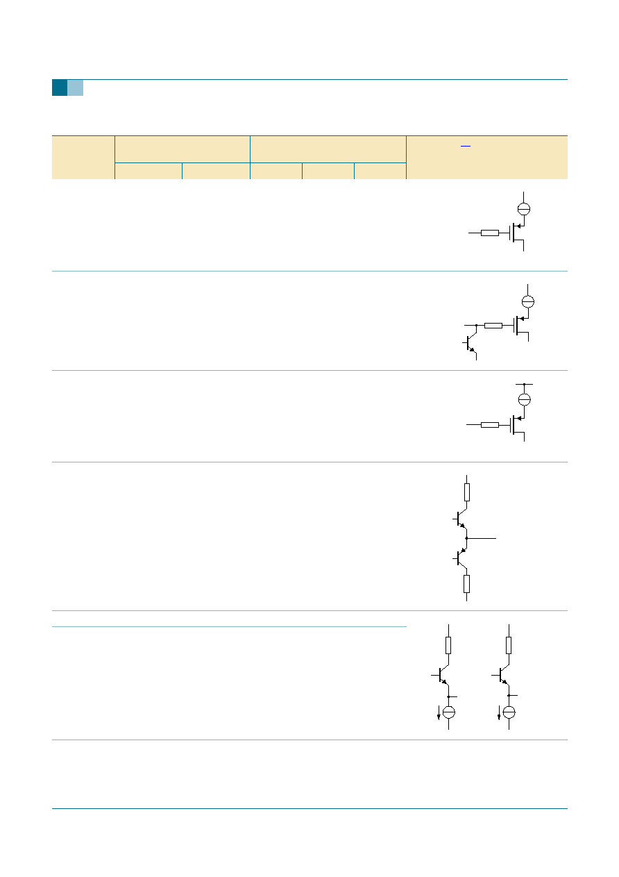
9.
Internal circuitry
Table 16:
Internal pin configuration
Symbol
Pin
Average DC voltage versus band
selection
Description
[1]
TDA6650ATT
TDA6651ATT
Low
Mid
High
HBIN1
1
38
n.a.
n.a
1.0 V
HBIN2
2
37
n.a.
n.a
1.0 V
MBIN
3
36
n.a.
1.8 V
n.a.
LBIN
4
35
1.8 V
n.a.
n.a
RFGND
5
34
-
-
-
IFFIL1
6
33
3.7 V
3.7 V
3.7 V
IFFIL2
7
32
3.7 V
3.7 V
3.7 V
BS4
8
31
high-Z or
V
CC
-
V
DS
high-Z or
V
CC
-
V
DS
high-Z or
V
CC
-
V
DS
fce899
(38) 1
2 (37)
fce901
(36) 3
fce898
(35) 4
fce897
5 (34)
fce896
7 (32)
(33) 6
fce895
8 (31)
9397 750 14179
� Koninklijke Philips Electronics N.V. 2004. All rights reserved.
Product data sheet
Rev. 01 -- 14 December 2004
15 of 53
Philips Semiconductors
TDA6650ATT; TDA6651ATT
5 V mixer/oscillator and low noise PLL synthesizer
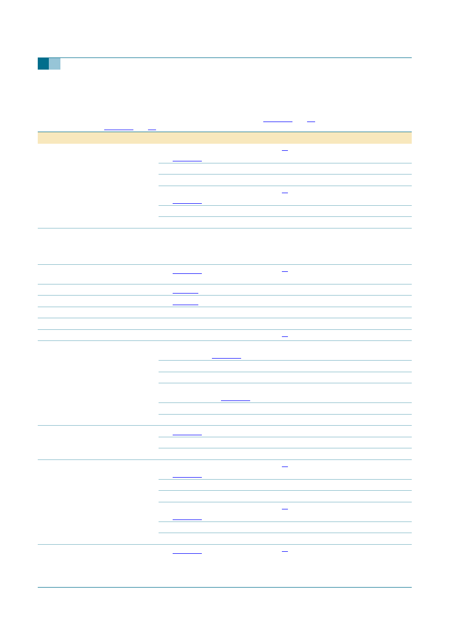
AGC
9
30
0 V or
3.5 V
0 V or
3.5 V
0 V or
3.5 V
BS3
10
29
high-Z or
V
CC
-
V
DS
high-Z or
V
CC
-
V
DS
high-Z or
V
CC
-
V
DS
BS2
11
28
high-Z
V
CC
-
V
DS
high-Z
BS1
12
27
V
CC
-
V
DS
high-Z
high-Z
BVS
13
26
2.5 V
2.5 V
2.5 V
ADC/BS5
14
25
V
CEsat
or
high-Z
V
CEsat
or
high-Z
V
CEsat
or
high-Z
Table 16:
Internal pin configuration
...continued
Symbol
Pin
Average DC voltage versus band
selection
Description
[1]
TDA6650ATT
TDA6651ATT
Low
Mid
High
fce907
9 (30)
fce893
10 (29)
fce892
11 (28)
fce891
12 (27)
mce163
(26) 13
fce887
(25) 14
9397 750 14179
� Koninklijke Philips Electronics N.V. 2004. All rights reserved.
Product data sheet
Rev. 01 -- 14 December 2004
16 of 53
Philips Semiconductors
TDA6650ATT; TDA6651ATT
5 V mixer/oscillator and low noise PLL synthesizer
SCL
15
24
high-Z
high-Z
high-Z
SDA
16
23
high-Z
high-Z
high-Z
AS
17
22
1.25 V
1.25 V
1.25 V
XTOUT
18
21
3.45 V
3.45 V
3.45 V
XTAL1
19
20
2.2 V
2.2 V
2.2 V
XTAL2
20
19
2.2 V
2.2 V
2.2 V
n.c.
21
18
n.a.
n.a.
n.a.
not connected
Table 16:
Internal pin configuration
...continued
Symbol
Pin
Average DC voltage versus band
selection
Description
[1]
TDA6650ATT
TDA6651ATT
Low
Mid
High
fce889
(24) 15
fce888
(23) 16
001aac102
(22) 17
mce164
18 (21)
19 (20)
20 (19)
fce883

9397 750 14179
� Koninklijke Philips Electronics N.V. 2004. All rights reserved.
Product data sheet
Rev. 01 -- 14 December 2004
17 of 53
Philips Semiconductors
TDA6650ATT; TDA6651ATT
5 V mixer/oscillator and low noise PLL synthesizer
VT
22
17
V
VT
V
VT
V
VT
CP
23
16
1.8 V
1.8 V
1.8 V
V
CCD
24
15
5 V
5 V
5 V
PLLGND
25
14
-
-
-
V
CCA
26
13
5 V
5 V
5 V
IFOUTB
27
12
2.1 V
2.1 V
2.1 V
IFOUTA
28
11
2.1 V
2.1 V
2.1 V
IFGND
29
10
-
-
-
HOSCIN1
30
9
2.2 V
2.2 V
1.8 V
HOSCOUT1
31
8
5 V
5 V
2.5 V
HOSCOUT2
32
7
5 V
5 V
2.5 V
HOSCIN2
33
6
2.2 V
2.2 V
1.8 V
Table 16:
Internal pin configuration
...continued
Symbol
Pin
Average DC voltage versus band
selection
Description
[1]
TDA6650ATT
TDA6651ATT
Low
Mid
High
fce884
22 (17)
fce885
23 (16)
fce882
25 (14)
fce886
28 (11)
fce880
29 (10)
fce879
(6) 33
32 (7)
30 (9)
(8) 31

9397 750 14179
� Koninklijke Philips Electronics N.V. 2004. All rights reserved.
Product data sheet
Rev. 01 -- 14 December 2004
18 of 53
Philips Semiconductors
TDA6650ATT; TDA6651ATT
5 V mixer/oscillator and low noise PLL synthesizer
[1]
The pin numbers in parenthesis refer to the TDA6651ATT.
10. Limiting values
MOSCIN1
34
5
2.3 V
1.3 V
2.3 V
MOSCIN2
35
4
2.3 V
1.3 V
2.3 V
OSCGND
36
3
-
-
-
LOSCOUT
37
2
1.7 V
1.4 V
1.4 V
LOSCIN
38
1
2.9 V
3.5 V
3.5 V
Table 16:
Internal pin configuration
...continued
Symbol
Pin
Average DC voltage versus band
selection
Description
[1]
TDA6650ATT
TDA6651ATT
Low
Mid
High
34 (5)
35 (4)
fce878
fce908
36 (3)
fce877
(1) 38
37 (2)
Table 17:
Limiting values
In accordance with the Absolute Maximum Rating System (IEC 60134). Positive currents are
entering the IC and negative currents are going out of the IC; all voltages are referenced to ground
(GND)
[1]
.
Symbol
Parameter
Conditions
Min
Max
Unit
V
CCA
,
V
CCD
supply voltage
-
0.3
+6
V
V
VT
tuning voltage output
-
0.3
+35
V
V
SDA
serial data input and output
voltage
-
0.3
+6
V
I
SDA
serial data output current
during
acknowledge
0
10
mA
V
SCL
serial clock input voltage
-
0.3
+6
V
V
AS
address selection input
voltage
-
0.3
+6
V

9397 750 14179
� Koninklijke Philips Electronics N.V. 2004. All rights reserved.
Product data sheet
Rev. 01 -- 14 December 2004
19 of 53
Philips Semiconductors
TDA6650ATT; TDA6651ATT
5 V mixer/oscillator and low noise PLL synthesizer
[1]
Maximum ratings cannot be exceeded, not even momentarily without causing irreversible IC damage.
Maximum ratings cannot be accumulated.
[2]
V
CC
refers to the operating supply voltage.
[3]
The maximum allowed ambient temperature T
amb(max)
depends on the assembly conditions of the package
and especially on the design of the printed-circuit board. The application mounting must be done in such a
way that the maximum junction temperature is never exceeded. An estimation of the junction temperature
can be obtained through measurement of the temperature of the top center of the package (T
package
). The
temperature difference junction to case (
T
j-c
) is estimated at about 13
�
C on the demo board (PCB 827-3).
The junction temperature T
j
= T
package
+
T
j-c
.
11. Thermal characteristics
[1]
Measured in free air as defined by JEDEC standard JESD51-2.
[2]
These values are given for information only. The thermal resistance depends strongly on the nature and
design of the printed-circuit board used in the application. The thermal resistance given corresponds to the
value that can be measured on a multilayer printed-circuit board (4 layers) as defined by JEDEC standard.
[3]
The junction temperature influences strongly the reliability of an IC. The printed-circuit board used in the
application contributes in a large part to the overall thermal characteristic. It must therefore be insured that
the junction temperature of the IC never exceeds T
j(max)
= 150
�
C at the maximum ambient temperature.
V
n
voltage on all other inputs,
outputs and combined
inputs and outputs, except
GNDs
4.5 V < V
CC
< 5.5 V
[2]
-
0.3
V
CC
+ 0.3
V
I
BSn
PMOS port output current
corresponding port
on; open-drain
-
20
0
mA
I
BS(tot)
sum of all PMOS port output
currents
open-drain
-
50
0
mA
t
sc(max)
maximum short-circuit time
each pin to V
CC
or
to GND
-
10
s
T
stg
storage temperature
-
40
+150
�
C
T
amb
ambient temperature
[3]
-
20
T
amb(max)
�
C
T
j
junction temperature
-
150
�
C
Table 17:
Limiting values
...continued
In accordance with the Absolute Maximum Rating System (IEC 60134). Positive currents are
entering the IC and negative currents are going out of the IC; all voltages are referenced to ground
(GND)
[1]
.
Symbol
Parameter
Conditions
Min
Max
Unit
Table 18:
Thermal characteristics
Symbol
Parameter
Conditions
Typ
Unit
R
th(j-a)
thermal resistance from
junction to ambient
[1] [2] [3]
TDA6650ATT
82
K/W
TDA6651ATT
74
K/W

9397 750 14179
� Koninklijke Philips Electronics N.V. 2004. All rights reserved.
Product data sheet
Rev. 01 -- 14 December 2004
20 of 53
Philips Semiconductors
TDA6650ATT; TDA6651ATT
5 V mixer/oscillator and low noise PLL synthesizer
12. Characteristics
Table 19:
Characteristics
V
CCA
= V
CCD
= 5 V; T
amb
= 25
�
C; values are given for an asymmetrical IF output loaded with a 75
load or with a
symmetrical IF output loaded with 1.25 k
; positive currents are entering the IC and negative currents are going out of the IC;
the performances of the circuits are measured in the measurement circuits
Figure 27
and
28
for digital application or in the
measurement circuits
Figure 29
and
30
for hybrid application; unless otherwise specified.
Symbol
Parameter
Conditions
Min
Typ
Max
Unit
Supply
V
CC
supply voltage
4.5
5.0
5.5
V
I
CC
supply current
PMOS ports off
80
96
115
mA
one PMOS port on: sourcing 15 mA
96
112
131
mA
two PMOS ports on: one port
sourcing 15 mA and one other port
sourcing 5 mA
101
117
136
mA
General functions
V
POR
power-on reset supply
voltage
power-on reset active if V
CC
< V
POR
-
2.85
3.5
V
f
lock
frequency range the PLL
is able to synthesize
64
-
1024
MHz
Crystal oscillator
[1]
f
xtal
crystal frequency
-
4.0
-
MHz
Z
xtal
input impedance
(absolute value)
f
xtal
= 4 MHz; V
CC
= 4.5 V to 5.5 V
T
amb
=
-
20
�
C to T
amb(max)
,
see
Section 10
350
430
-
P
xtal
crystal drive level
f
xtal
= 4 MHz
[2]
-
70
-
�
W
PMOS ports: pins BS1, BS2, BS3, BS4 and BS5
I
LO(off)
output leakage current in
off state
V
CC
= 5.5 V; V
BS
= 0 V
-
10
-
-
�
A
V
DS(sat)
output saturation voltage only corresponding buffer is on,
sourcing 15 mA;
V
DS(sat)
= V
CC
-
V
BS
-
0.2
0.4
V
ADC input: pin ADC
V
i
ADC input voltage
see
Table 14
0
-
5.5
V
I
IH
HIGH-level input current
V
ADC
= V
CC
-
-
10
�
A
I
IL
LOW-level input current
V
ADC
= 0 V
-
10
-
-
�
A
Address selection input: pin AS
I
IH
HIGH-level input current
V
AS
= 5.5 V
-
-
10
�
A
I
IL
LOW-level input current
V
AS
= 0 V
-
10
-
-
�
A
Bus voltage selection input: pin BVS
I
IH
HIGH-level input current
V
BVS
= 5.5 V
-
-
100
�
A
I
IL
LOW-level input current
V
BVS
= 0 V
-
100
-
-
�
A
Buffered output: pin XTOUT
V
o(p-p)
square wave AC output
voltage (peak-to-peak
value)
[3]
-
400
-
mV
Z
o
output impedance
-
175
-

9397 750 14179
� Koninklijke Philips Electronics N.V. 2004. All rights reserved.
Product data sheet
Rev. 01 -- 14 December 2004
21 of 53
Philips Semiconductors
TDA6650ATT; TDA6651ATT
5 V mixer/oscillator and low noise PLL synthesizer
I
2
C-bus
Inputs: pins SCL and SDA
f
clk
clock frequency
frequency on SCL
-
-
400
kHz
V
IL
LOW-level input voltage
V
BVS
= 0 V
0
-
0.75
V
V
BVS
= 2.5 V or open-circuit
0
-
1.0
V
V
BVS
= 5 V
0
-
1.5
V
V
IH
HIGH-level input voltage V
BVS
= 0 V
1.75
-
5.5
V
V
BVS
= 2.5 V or open-circuit
2.3
-
5.5
V
V
BVS
= 5 V
3.0
-
5.5
V
I
IH
HIGH-level input current
V
CC
= 0 V; V
BUS
= 5.5 V
-
-
10
�
A
V
CC
= 5.5 V; V
BUS
= 5.5 V
-
-
10
�
A
I
IL
LOW-level input current
V
CC
= 0 V; V
BUS
= 1.5 V
-
-
10
�
A
V
CC
= 5.5 V; V
BUS
= 0 V
-
10
-
-
�
A
Output: pin SDA
I
LH
leakage current
V
SDA
= 5.5 V
-
-
10
�
A
V
O(ack)
output voltage during
acknowledge
I
SDA
= 3 mA
-
-
0.4
V
Charge pump output: pin CP
I
o
output current (absolute
value)
see
Table 11
-
-
-
�
A
I
L(off)
off-state leakage current charge pump off (T[2:0] = 010)
-
15
0
+15
nA
Tuning voltage output: pin VT
I
L(off)
leakage current when
switched-off
tuning supply voltage = 33 V
-
-
10
�
A
V
o(cl)
output voltage when the
loop is closed
tuning supply voltage = 33 V;
R
L
= 15 k
0.3
-
32.7
V
Noise performance
J
(rms)
phase jitter (RMS value)
integrated between 1 kHz and
1 MHz offset from the carrier
digital application
-
0.5
-
deg
hybrid application
-
0.6
-
deg
Low band mixer, including IF amplifier
f
RF
RF frequency
picture carrier
[4]
91.25
-
219.143 MHz
Table 19:
Characteristics
...continued
V
CCA
= V
CCD
= 5 V; T
amb
= 25
�
C; values are given for an asymmetrical IF output loaded with a 75
load or with a
symmetrical IF output loaded with 1.25 k
; positive currents are entering the IC and negative currents are going out of the IC;
the performances of the circuits are measured in the measurement circuits
Figure 27
and
28
for digital application or in the
measurement circuits
Figure 29
and
30
for hybrid application; unless otherwise specified.
Symbol
Parameter
Conditions
Min
Typ
Max
Unit

9397 750 14179
� Koninklijke Philips Electronics N.V. 2004. All rights reserved.
Product data sheet
Rev. 01 -- 14 December 2004
22 of 53
Philips Semiconductors
TDA6650ATT; TDA6651ATT
5 V mixer/oscillator and low noise PLL synthesizer
G
v
voltage gain
asymmetrical IF output; R
L
= 75
;
see
Figure 14
f
RF
= 91.25 MHz
20
23.5
26
dB
f
RF
= 219.143 MHz
20
24.0
26
dB
symmetrical IF output;
R
L
= 1.25 k
; see
Figure 15
f
RF
= 91.25 MHz
25
27.5
31
dB
f
RF
= 219.143 MHz
25
27.5
31
dB
NF
noise figure
f
RF
= 150 MHz
-
7
10
dB
V
o
output voltage causing
1 % cross modulation in
channel
asymmetrical application;
see
Figure 18
[5]
f
RF
= 91.25 MHz
107
110
-
dB
�
V
f
RF
= 219.143 MHz
107
110
-
dB
�
V
symmetrical application;
see
Figure 19
[5]
f
RF
= 91.25 MHz
117
120
-
dB
�
V
f
RF
= 219.143 MHz
117
120
-
dB
�
V
V
i
input voltage causing
750 Hz frequency
deviation pulling in
channel
asymmetrical IF output
-
85
-
dB
�
V
V
i(lock)
input level without
lock-out
see
Figure 25
[7]
-
-
120
dB
�
V
G
i
input conductance
f
RF
= 91.25 MHz; see
Figure 5
-
0.15
-
mS
f
RF
= 219.43 MHz; see
Figure 5
-
0.20
-
mS
C
i
input capacitance
f
RF
= 91.25 MHz to 219.43 MHz;
see
Figure 5
-
1.60
-
pF
Mid band mixer, including IF amplifier
f
oper
operating frequency
163.25
-
465.143 MHz
f
RF
RF frequency
picture carrier
[4]
223.25
-
465.143 MHz
G
v
voltage gain
asymmetrical IF output;
load = 75
; see
Figure 14
f
RF
= 223.25 MHz
20
23.5
26
dB
f
RF
= 465.143 MHz
20
24
26
dB
symmetrical IF output;
load = 1.25 k
; see
Figure 15
f
RF
= 223.25 MHz
25
27
31
dB
f
RF
= 465.143 MHz
25
27.5
31
dB
NF
noise figure
f
RF
= 300 MHz; see
Figure 17
-
8
11
dB
Table 19:
Characteristics
...continued
V
CCA
= V
CCD
= 5 V; T
amb
= 25
�
C; values are given for an asymmetrical IF output loaded with a 75
load or with a
symmetrical IF output loaded with 1.25 k
; positive currents are entering the IC and negative currents are going out of the IC;
the performances of the circuits are measured in the measurement circuits
Figure 27
and
28
for digital application or in the
measurement circuits
Figure 29
and
30
for hybrid application; unless otherwise specified.
Symbol
Parameter
Conditions
Min
Typ
Max
Unit
9397 750 14179
� Koninklijke Philips Electronics N.V. 2004. All rights reserved.
Product data sheet
Rev. 01 -- 14 December 2004
23 of 53
Philips Semiconductors
TDA6650ATT; TDA6651ATT
5 V mixer/oscillator and low noise PLL synthesizer
V
o
output voltage causing
1 % cross modulation in
channel
asymmetrical application;
see
Figure 18
[5]
f
RF
= 223.25 MHz
107
110
-
dB
�
V
f
RF
= 465.143 MHz
107
110
-
dB
�
V
symmetrical application;
see
Figure 19
[5]
f
RF
= 223.25 MHz
117
120
-
dB
�
V
f
RF
= 465.143 MHz
117
120
-
dB
�
V
V
i
input voltage causing
750 Hz frequency
deviation pulling in
channel
asymmetrical IF output
-
87
-
dB
�
V
V
i(lock)
input level without
lock-out
see
Figure 25
[7]
-
-
120
dB
�
V
G
i
input conductance
see
Figure 6
-
0.3
-
mS
C
i
input capacitance
see
Figure 6
-
1.1
-
pF
High band mixer, including IF amplifier
f
oper
operating frequency
355.25
-
767.143 MHz
f
RF
RF frequency
picture carrier
[4]
471.25
-
767.143 MHz
G
v
voltage gain
asymmetrical IF output;
load = 75
; see
Figure 20
f
RF
= 471.25 MHz
31.5
35
37.5
dB
f
RF
= 767.143 MHz
31.5
33.5
37.5
dB
symmetrical IF output;
load = 1.25 k
; see
Figure 21
f
RF
= 471.25 MHz
35.5
38.5
41.5
dB
f
RF
= 767.143 MHz
35.5
37
41.5
dB
NF
noise figure, not
corrected for image
see
Figure 22
f
RF
= 471.25 MHz
-
6
8
dB
f
RF
= 767.143 MHz
-
7
9
dB
V
o
output voltage causing
1 % cross modulation in
channel
asymmetrical application;
see
Figure 23
[5]
f
RF
= 471.25 MHz
107
110
-
dB
�
V
f
RF
= 767.143 MHz
107
110
-
dB
�
V
symmetrical application;
see
Figure 24
[5]
f
RF
= 471.25 MHz
117
120
-
dB
�
V
f
RF
= 767.143 MHz
117
120
-
dB
�
V
V
i(lock)
input level without
lock-out
see
Figure 26
[7]
-
-
120
dB
�
V
Table 19:
Characteristics
...continued
V
CCA
= V
CCD
= 5 V; T
amb
= 25
�
C; values are given for an asymmetrical IF output loaded with a 75
load or with a
symmetrical IF output loaded with 1.25 k
; positive currents are entering the IC and negative currents are going out of the IC;
the performances of the circuits are measured in the measurement circuits
Figure 27
and
28
for digital application or in the
measurement circuits
Figure 29
and
30
for hybrid application; unless otherwise specified.
Symbol
Parameter
Conditions
Min
Typ
Max
Unit

9397 750 14179
� Koninklijke Philips Electronics N.V. 2004. All rights reserved.
Product data sheet
Rev. 01 -- 14 December 2004
24 of 53
Philips Semiconductors
TDA6650ATT; TDA6651ATT
5 V mixer/oscillator and low noise PLL synthesizer
V
i
input voltage causing
750 Hz frequency
deviation pulling in
channel
asymmetrical IF output
-
75
-
dB
�
V
Z
i
input impedance
(R
S
+ jL
S
)
f
RF
= 471.25 MHz; see
Figure 7
R
S
-
35
-
L
S
-
8
-
nH
f
RF
= 767.143 MHz; see
Figure 7
R
S
-
36
-
L
S
-
8
-
nH
Low band oscillator
f
osc
oscillator frequency
[7]
150
-
276.143 MHz
f
osc(V)
oscillator frequency shift
with supply voltage
[8]
-
110
300
kHz
f
osc(T)
oscillator frequency drift
with temperature
T = 25
�
C; V
CC
= 5 V with
compensation
[9]
-
900
-
kHz
osc(dig)
phase noise, carrier to
sideband noise in digital
application
�
1 kHz frequency offset;
f
comp
= 4 MHz; see
Figure 8
,
27
and
28
82
90
-
dBc/Hz
�
10 kHz frequency offset; worst
case in the frequency range; see
Figure 9
,
27
and
28
87
94
-
dBc/Hz
�
100 kHz frequency offset; worst
case in the frequency range; see
Figure 10
,
27
and
28
104
115
-
dBc/Hz
�
1.4 MHz frequency offset; worst
case in the frequency range; see
Figure 27
and
28
-
117
-
dBc/Hz
osc(hyb)
phase noise, carrier to
sideband noise in hybrid
application
�
1 kHz frequency offset;
f
comp
= 4 MHz; see
Figure 11
,
29
and
30
75
81
-
dBc/Hz
�
10 kHz frequency offset; worst
case in the frequency range; see
Figure 12
,
29
and
30
85
92
-
dBc/Hz
�
100 kHz frequency offset; worst
case in the frequency range; see
Figure 13
,
29
and
30
104
115
-
dBc/Hz
�
1.4 MHz frequency offset; worst
case in the frequency range; see
Figure 29
and
30
-
117
-
dBc/Hz
RSC
p-p
ripple susceptibility of
V
CC
(peak-to-peak
value)
V
CC
= 5 V
�
5 %; worst case in the
frequency range; ripple frequency
500 kHz
[10]
15
200
-
mV
Table 19:
Characteristics
...continued
V
CCA
= V
CCD
= 5 V; T
amb
= 25
�
C; values are given for an asymmetrical IF output loaded with a 75
load or with a
symmetrical IF output loaded with 1.25 k
; positive currents are entering the IC and negative currents are going out of the IC;
the performances of the circuits are measured in the measurement circuits
Figure 27
and
28
for digital application or in the
measurement circuits
Figure 29
and
30
for hybrid application; unless otherwise specified.
Symbol
Parameter
Conditions
Min
Typ
Max
Unit

9397 750 14179
� Koninklijke Philips Electronics N.V. 2004. All rights reserved.
Product data sheet
Rev. 01 -- 14 December 2004
25 of 53
Philips Semiconductors
TDA6650ATT; TDA6651ATT
5 V mixer/oscillator and low noise PLL synthesizer
Mid band oscillator
f
osc
oscillator operating
frequency
222
-
522.143 MHz
oscillator frequency
[7]
276
-
522.143 MHz
f
osc(V)
oscillator frequency shift
with supply voltage
[8]
-
300
-
kHz
f
osc(T)
oscillator frequency drift
with temperature
T = 25
�
C; V
CC
= 5 V with
compensation
[9]
-
1500
-
kHz
osc(dig)
phase noise, carrier to
sideband noise in digital
application
�
1 kHz frequency offset;
f
comp
= 4 MHz; see
Figure 8
,
27
and
28
85
90
-
dBc/Hz
�
10 kHz frequency offset; worst
case in the frequency range; see
Figure 9
,
27
and
28
87
94
-
dBc/Hz
�
100 kHz frequency offset; worst
case in the frequency range; see
Figure 10
,
27
and
28
104
112
-
dBc/Hz
�
1.4 MHz frequency offset; worst
case in the frequency range; see
Figure 27
and
28
-
116
-
dBc/Hz
osc(hyb)
phase noise, carrier to
sideband noise in hybrid
application
�
1 kHz frequency offset;
f
comp
= 4 MHz; see
Figure 11
,
29
and
30
80
86
-
dBc/Hz
�
10 kHz frequency offset; worst
case in the frequency range; see
Figure 12
,
29
and
30
85
92
-
dBc/Hz
�
100 kHz frequency offset; worst
case in the frequency range; see
Figure 13
,
29
and
30
104
115
-
dBc/Hz
�
1.4 MHz frequency offset; worst
case in the frequency range; see
Figure 29
and
30
-
115
-
dBc/Hz
RSC
p-p
ripple susceptibility of
V
CC
(peak-to-peak
value)
V
CC
= 5 V
�
5%; worst case in the
frequency range; ripple frequency
500 kHz
[10]
15
140
-
mV
High band oscillator
f
osc
oscillator operating
frequency
414
-
824.143 MHz
oscillator frequency
[7]
522
-
824.143 MHz
f
osc(V)
oscillator frequency shift
with supply voltage
[8]
-
300
-
kHz
f
osc(T)
oscillator frequency drift
with temperature
T = 25
�
C; V
CC
= 5 V; with
compensation
[9]
-
1100
-
kHz
Table 19:
Characteristics
...continued
V
CCA
= V
CCD
= 5 V; T
amb
= 25
�
C; values are given for an asymmetrical IF output loaded with a 75
load or with a
symmetrical IF output loaded with 1.25 k
; positive currents are entering the IC and negative currents are going out of the IC;
the performances of the circuits are measured in the measurement circuits
Figure 27
and
28
for digital application or in the
measurement circuits
Figure 29
and
30
for hybrid application; unless otherwise specified.
Symbol
Parameter
Conditions
Min
Typ
Max
Unit

9397 750 14179
� Koninklijke Philips Electronics N.V. 2004. All rights reserved.
Product data sheet
Rev. 01 -- 14 December 2004
26 of 53
Philips Semiconductors
TDA6650ATT; TDA6651ATT
5 V mixer/oscillator and low noise PLL synthesizer
osc(dig)
phase noise, carrier to
sideband noise in digital
application
�
1 kHz frequency offset;
f
comp
= 4 MHz; see
Figure 8
,
27
and
28
80
85
-
dBc/Hz
�
10 kHz frequency offset; worst
case in the frequency range; see
Figure 9
,
27
and
28
85
91
-
dBc/Hz
�
100 kHz frequency offset; worst
case in the frequency range; see
Figure 11
,
27
and
28
104
112
-
dBc/Hz
�
1.4 MHz frequency offset; worst
case in the frequency range; see
Figure 27
and
28
-
117
-
dBc/Hz
osc(hyb)
phase noise, carrier to
sideband noise in hybrid
application
�
1 kHz frequency offset;
f
comp
= 4 MHz; see
Figure 11
,
29
and
30
80
86
-
dBc/Hz
�
10 kHz frequency offset; worst
case in the frequency range; see
Figure 12
,
29
and
30
82
88
-
dBc/Hz
�
100 kHz frequency offset; worst
case in the frequency range; see
Figure 13
,
29
and
30
104
112
-
dBc/Hz
�
1.4 MHz frequency offset; worst
case in the frequency range; see
Figure 29
and
30
-
117
-
dBc/Hz
RSC
p-p
ripple susceptibility of
V
CC
(peak-to-peak
value)
V
CC
= 5 V
�
5 %; worst case in the
frequency range; ripple frequency
500 kHz
[10]
15
40
-
mV
IF amplifier
Z
o
output impedance
asymmetrical IF output
R
S
at 57 MHz
-
50
-
L
S
at 57 MHz
-
4.7
-
nH
symmetrical IF output
R
S
at 57 MHz
-
100
-
L
S
at 57 MHz
-
10
-
nH
Rejection at the IF output (IF amplifier in asymmetrical mode)
INT
div
divider interferences in
IF level
worst case
[11]
-
-
20
dB
�
V
INT
xtal
crystal oscillator
interferences rejection
V
IF
= 100 dB
�
V; worst case in the
frequency range
[12]
-
-
-
50
dBc
INT
f(step)
step frequency rejection
V
IF
= 100 dB
�
V; worst case in the
frequency range
[13]
digital application
-
-
-
50
dBc
hybrid application
-
-
-
57
dBc
Table 19:
Characteristics
...continued
V
CCA
= V
CCD
= 5 V; T
amb
= 25
�
C; values are given for an asymmetrical IF output loaded with a 75
load or with a
symmetrical IF output loaded with 1.25 k
; positive currents are entering the IC and negative currents are going out of the IC;
the performances of the circuits are measured in the measurement circuits
Figure 27
and
28
for digital application or in the
measurement circuits
Figure 29
and
30
for hybrid application; unless otherwise specified.
Symbol
Parameter
Conditions
Min
Typ
Max
Unit

9397 750 14179
� Koninklijke Philips Electronics N.V. 2004. All rights reserved.
Product data sheet
Rev. 01 -- 14 December 2004
27 of 53
Philips Semiconductors
TDA6650ATT; TDA6651ATT
5 V mixer/oscillator and low noise PLL synthesizer
[1]
Important recommendation: to obtain the performances mentioned in this specification, the serial resistance of the crystal used with this
oscillator must never exceed 120
. The crystal oscillator is guaranteed to operate at any supply voltage between 4.5 V and 5.5 V and
at any temperature between
-
20
�
C and + T
amb(max)
, as defined in
Section 10
.
[2]
The drive level is expected with a 50
series resistance of the crystal at series resonance. The drive level will be different with other
series resistance values.
[3]
The V
XTOUT
level is measured when the pin XTOUT is loaded with 5 k
in parallel with 10 pF.
[4]
The RF frequency range is defined by the oscillator frequency range and the intermediate frequency (IF).
[5]
The 1 % cross modulation performance is measured with AGC detector turned off (AGC bits set to 110).
[6]
The IF output signal stays stable within the range of the step frequency for any RF input level up to 120 dB
�
V.
[7]
Limits are related to the tank circuits used in
Figure 27
and
28
for digital application or
Figure 29
and
30
for hybrid application.
Frequency bands may be adjusted by the choice of external components.
[8]
The frequency shift is defined as a change in oscillator frequency when the supply voltage varies from V
CC
= 5 V to 4.5 V or from
V
CC
= 5 V to 5.25 V. The oscillator is free running during this measurement.
[9]
The frequency drift is defined as a change in oscillator frequency when the ambient temperature varies from T
amb
= 25
�
C to 50
�
C or
from T
amb
= 25
�
C to 0
�
C. The oscillator is free running during this measurement.
[10] The supply ripple susceptibility is measured in the measurement circuit according to
Figure 27
to
Figure 30
using a spectrum analyzer
connected to the IF output. An unmodulated RF signal is applied to the test board RF input. A sinewave signal with a frequency of
500 kHz is superimposed onto the supply voltage. The amplitude of this ripple signal is adjusted to bring the 500 kHz sidebands around
the IF carrier to a level of
-
53.5 dB with respect to the carrier.
[11] This is the level of divider interferences close to the IF frequency. The low and mid band inputs must be left open (i.e. not connected to
any load or cable); the high band inputs are connected to an hybrid.
[12] Crystal oscillator interference means the 4 MHz sidebands caused by the crystal oscillator.
[13] The step frequency rejection is the level of step frequency sidebands related to the carrier. The measurement is done for
V
IF
= 100 dB
�
V. This specification point corresponds to the worst case observed in the frequency range. This parameter is specified for
f
step
= 142.86 kHz in digital applications and f
step
= 62.5 kHz, 50 kHz or 142.86 kHz in hybrid application.
INT
XTH
crystal oscillator
harmonics in the
IF frequency
[14]
-
-
50
dB
�
V
AGC output (IF amplifier in asymmetrical mode): pin AGC
AGC
TOP(p-p)
AGC take-over point
(peak-to-peak level)
bits AL[2:0] = 000
122.5
124
125.5
dB
�
V
I
source(fast)
source current fast
7.5
9.0
11.6
�
A
I
source(slow)
source current slow
185
220
280
nA
V
o
output voltage
maximum level
3.45
3.55
3.8
V
minimum level
0
-
0.1
V
V
o(dis)
output voltage with AGC
disabled
bits AL[2:0] = 111
3.45
3.55
3.8
V
V
RF(slip)
RF voltage range to
switch the AGC from
active to not active mode
-
-
0.5
dB
V
RML
low threshold AGC
output voltage
AGC bit = 0 or AGC not active
0
-
2.8
V
V
RMH
high threshold AGC
output voltage
AGC bit = 1 or AGC active
3.2
3.55
3.8
V
I
LO
leakage current
bits AL[2:0] = 110; 0 < V
AGC
< V
CC
-
50
-
+50
nA
Table 19:
Characteristics
...continued
V
CCA
= V
CCD
= 5 V; T
amb
= 25
�
C; values are given for an asymmetrical IF output loaded with a 75
load or with a
symmetrical IF output loaded with 1.25 k
; positive currents are entering the IC and negative currents are going out of the IC;
the performances of the circuits are measured in the measurement circuits
Figure 27
and
28
for digital application or in the
measurement circuits
Figure 29
and
30
for hybrid application; unless otherwise specified.
Symbol
Parameter
Conditions
Min
Typ
Max
Unit

9397 750 14179
� Koninklijke Philips Electronics N.V. 2004. All rights reserved.
Product data sheet
Rev. 01 -- 14 December 2004
28 of 53
Philips Semiconductors
TDA6650ATT; TDA6651ATT
5 V mixer/oscillator and low noise PLL synthesizer
[14] This is the level of the 13rd and 15th harmonics of the 4 MHz crystal oscillator into the IF output.
Fig 5.
Input admittance (s
11
) of the low band mixer (40 MHz to 200 MHz); Y
o
= 20 mS
Fig 6.
Input admittance (s
11
) of the mid band mixer (100 MHz to 500 MHz); Y
o
= 20 mS
mce160
0.2
2
1
0.5
10
5
0.2
2
1
0.5
10
5
0
+
j
-
j
0.2
0.5
1
2
5
10
40 MHz
200 MHz
mce161
0.2
2
1
0.5
10
5
0.2
2
1
0.5
10
5
0
+
j
-
j
0.2
0.5
1
2
5
10
100 MHz
500 MHz

9397 750 14179
� Koninklijke Philips Electronics N.V. 2004. All rights reserved.
Product data sheet
Rev. 01 -- 14 December 2004
29 of 53
Philips Semiconductors
TDA6650ATT; TDA6651ATT
5 V mixer/oscillator and low noise PLL synthesizer
Fig 7.
Input impedance (s
11
) of the high band mixer (350 MHz to 800 MHz); Z
o
= 100
0.2
0.5
1
2
5
10
0.2
0.5
1
2
5
10
0
+
j
-
j
001aac088
0.5
1
0.2
10
5
2
800 MHz
350 MHz
Fig 8.
1 kHz phase noise typical performance in digital application (
Figure 27
and
28
)
001aac089
-
90
-
95
-
85
-
80
-
100
150
250
350
450
550
650
750
850
f
RF
(MHz)
osc
(dBc/Hz)

9397 750 14179
� Koninklijke Philips Electronics N.V. 2004. All rights reserved.
Product data sheet
Rev. 01 -- 14 December 2004
30 of 53
Philips Semiconductors
TDA6650ATT; TDA6651ATT
5 V mixer/oscillator and low noise PLL synthesizer
Fig 9.
10 kHz phase noise typical performance in digital application (
Figure 27
and
28
)
001aac090
-
95
-
100
-
90
-
85
-
105
150
250
350
450
550
650
750
850
f
RF
(MHz)
osc
(dBc/Hz)
Fig 10. 100 kHz phase noise typical performance in digital application (
Figure 27
and
28
)
001aac091
-
115
-
110
-
105
-
120
150
250
350
450
550
650
750
850
f
RF
(MHz)
osc
(dBc/Hz)

9397 750 14179
� Koninklijke Philips Electronics N.V. 2004. All rights reserved.
Product data sheet
Rev. 01 -- 14 December 2004
31 of 53
Philips Semiconductors
TDA6650ATT; TDA6651ATT
5 V mixer/oscillator and low noise PLL synthesizer
Fig 11. 1 kHz phase noise typical performance in hybrid application (
Figure 29
and
30
)
001aac092
-
90
-
95
-
85
-
80
-
75
-
100
150
250
350
450
550
650
750
850
f
RF
(MHz)
osc
(dBc/Hz)
Fig 12. 10 kHz phase noise typical performance in hybrid application (
Figure 29
and
30
)
001aac093
-
95
-
90
-
85
-
100
150
250
350
450
550
650
750
850
f
RF
(MHz)
osc
(dBc/Hz)
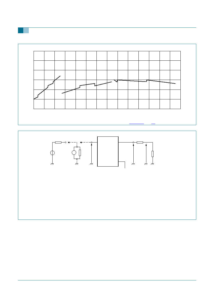
9397 750 14179
� Koninklijke Philips Electronics N.V. 2004. All rights reserved.
Product data sheet
Rev. 01 -- 14 December 2004
32 of 53
Philips Semiconductors
TDA6650ATT; TDA6651ATT
5 V mixer/oscillator and low noise PLL synthesizer
Fig 13. 100 kHz phase noise typical performance in hybrid application (
Figure 29
and
30
)
001aac094
-
115
-
110
-
105
-
120
150
250
350
450
550
650
750
850
f
RF
(MHz)
osc
(dBc/Hz)
Z
i
>> 50
V
i
= 2
�
V
meas
= 70 dB
�
V.
V
i
= V
meas
+ 6 dB = 70 dB
�
V.
V
o
= V'
meas
+ 3.75 dB.
.
ISDBT and NTSC-Japan.
IF = 57 MHz.
Fig 14. Gain (G
V
) measurement in low and mid band with asymmetrical IF output
fce747
V
LBIN
or
MBIN
IFOUTA
e
DUT
IFOUTB
V
CCA
50
signal
source
V'
meas
V
meas
RMS
voltmeter
50
50
spectrum
analyzer
27
Vo
V
i
G
v
20
V
o
V
i
------
log
=

9397 750 14179
� Koninklijke Philips Electronics N.V. 2004. All rights reserved.
Product data sheet
Rev. 01 -- 14 December 2004
33 of 53
Philips Semiconductors
TDA6650ATT; TDA6651ATT
5 V mixer/oscillator and low noise PLL synthesizer
Z
i
>> 50
V
i
= 2
�
V
meas
= 70 dB
�
V.
V
i
= V
meas
+ 6 dB = 70 dB
�
V.
V
o
= V'
meas
+ 15 dB (transformer ratio N1/N2 = 5 and transformer loss).
.
ISDBT and NTSC-Japan.
IF = 57 MHz.
N1 = 10 turns.
N2 = 2 turns.
N1/N2 = 5.
Fig 15. Gain (G
V
) measurement in low and mid band with symmetrical IF output
NF = NF
meas
-
loss of input circuit (dB).
Fig 16. Noise figure (NF) measurement in low and mid band with asymmetrical IF output
fce748
V
IFOUTA
e
DUT
IFOUTB
C
N1
N2
transformer
50
signal
source
LBIN
or
MBIN
V
meas
V'
meas
RMS
voltmeter
50
50
spectrum
analyzer
V
o
V
i
G
v
20
V
o
V
i
------
log
=
fce750
LBIN
or
MBIN
IFOUTA
DUT
NOISE
SOURCE
NOISE
FIGURE
METER
BNC
RIM
INPUT
CIRCUIT
IFOUTB
V
CCA
27

9397 750 14179
� Koninklijke Philips Electronics N.V. 2004. All rights reserved.
Product data sheet
Rev. 01 -- 14 December 2004
34 of 53
Philips Semiconductors
TDA6650ATT; TDA6651ATT
5 V mixer/oscillator and low noise PLL synthesizer
a. Schematic 1
b. Schematic 2
For f
RF
= 150 MHz
Loss = 0 dB.
Cs = 0.8 pF to 8 pF trimmer.
Cp = 0.4 pF to 2.5 pF trimmer.
Lp = 4 turns, 4.5 mm, 0.4 mm wire air coil.
Cc = 4.7 nF.
TL: 50
semi rigid cable length = 75 mm.
For f
RF
= 300 MHz.
Loss = 0.5 dB.
Ls = 2 turns, 1.5 mm, 0.4 mm wire air coil.
Cp = 8.2 pF in parallel with a 0.8 pF to 8 pF trimmer.
Lp = 2 turns, 1.5 mm, 0.4 mm wire air coi.
Cc = 4.7 nF.
TL: 50
semi rigid cable length = 75 mm.
Fig 17. Input circuit for optimum noise figure measurement
mce452
Lp
Cp
Cs
Cc
TL
to the IC
mixer input
Lp
Cp
Ls
Cc
TL
to the IC
mixer input
BNC
connector
BNC
connector
V
o
= V
meas
+ 3.75 dB.
V'
meas
= V
o
-
(transformer ratio N1/N2 = 5 and loss).
Wanted signal source at f
RFpix
is 80 dB
�
V.
Unwanted output signal at f
snd
.
The level of unwanted signal is measured by causing 0.3 % AM modulation in the wanted signal.
N1 = 10 turns.
N2 = 2 turns.
N1/N2 = 5.
Fig 18. Cross modulation measurement in low and mid band with asymmetrical IF output
57 MHz
V
A
B
C
D
HYBRID
FILTER
LBIN
or
MBIN
IFOUTA
DUT
IFOUTB
V
CCA
001aac095
50
wanted
signal
source
unwanted
signal
source
AM = 30%
1 kHz
10 dB
attenuator
V
meas
RMS
voltmeter
50
50
e
u
e
w
50
modulation
analyzer
27
V
o

9397 750 14179
� Koninklijke Philips Electronics N.V. 2004. All rights reserved.
Product data sheet
Rev. 01 -- 14 December 2004
35 of 53
Philips Semiconductors
TDA6650ATT; TDA6651ATT
5 V mixer/oscillator and low noise PLL synthesizer
V'
meas
= V
o
-
(transformer ratio N1/N2 = 5 and loss).
Wanted signal source at f
RFpix
is 80 dB
�
V.
The level of unwanted signal V
o
at f
snd
is measured by causing 0.3 % AM modulation in the wanted output signal.
N1 = 10 turns.
N2 = 2 turns.
N1/N2 = 5.
Fig 19. Cross modulation measurement in low and mid band with symmetrical IF output
A
B
C
D
HYBRID
IFOUTA
IFOUTB
001aac096
C
N1
N2
transformer
V
FILTER
57 MHz
50
wanted
signal
source
unwanted
signal
source
AM = 30%
1 kHz
LBIN
or
MBIN
6 dB
attenuator
V'
meas
RMS
voltmeter
DUT
50
50
e
u
e
w
50
modulation
analyzer
V
o
Loss in hybrid = 1 dB.
V
i
= V
meas
-
loss = 70 dB
�
V.
V
o
= V'
meas
+ 3.75 dB.
.
ISDBT and NTSC-Japan.
IF = 57 MHz.
Fig 20. Gain (G
V
) measurement in high band with asymmetrical IF output
fce751
V
IFOUTA
DUT
A
B
C
D
HYBRID
IFOUTB
V
CCA
e
50
50
signal
source
HBIN1
HBIN2
V
meas
RMS
voltmeter
50
50
spectrum
analyzer
27
V
'
meas
V
i
V
o
G
v
20
V
o
V
i
------
log
=

9397 750 14179
� Koninklijke Philips Electronics N.V. 2004. All rights reserved.
Product data sheet
Rev. 01 -- 14 December 2004
36 of 53
Philips Semiconductors
TDA6650ATT; TDA6651ATT
5 V mixer/oscillator and low noise PLL synthesizer
Loss in hybrid = 1 dB.
V
i
= V
meas
-
loss = 70 dB
�
V.
V
o
= V'
meas
+ 15 dB (transformer ratio N1/N2 = 5 and transformer loss).
.
ISDBT and NTSC-Japan.
IF = 57 MHz.
Fig 21. Gain (G
V
) measurement in high band with symmetrical IF output
Loss in hybrid = 1 dB.
NF = NF
meas
-
loss.
Fig 22. Noise figure (NF) measurement in high band with asymmetrical IF output
fce752
V
IFOUTA
DUT
A
B
C
D
HYBRID
IFOUTB
e
C
N1
N2
transformer
50
50
signal
source
HBIN1
HBIN2
V
meas
V'
meas
RMS
voltmeter
50
50
spectrum
analyzer
V
o
V
i
G
v
20
V
o
V
i
------
log
=
fce753
DUT
NOISE
SOURCE
NOISE
FIGURE
METER
A
B
C
D
HYBRID
IFOUTA
IFOUTB
V
CCA
50
HBIN1
HBIN2
27
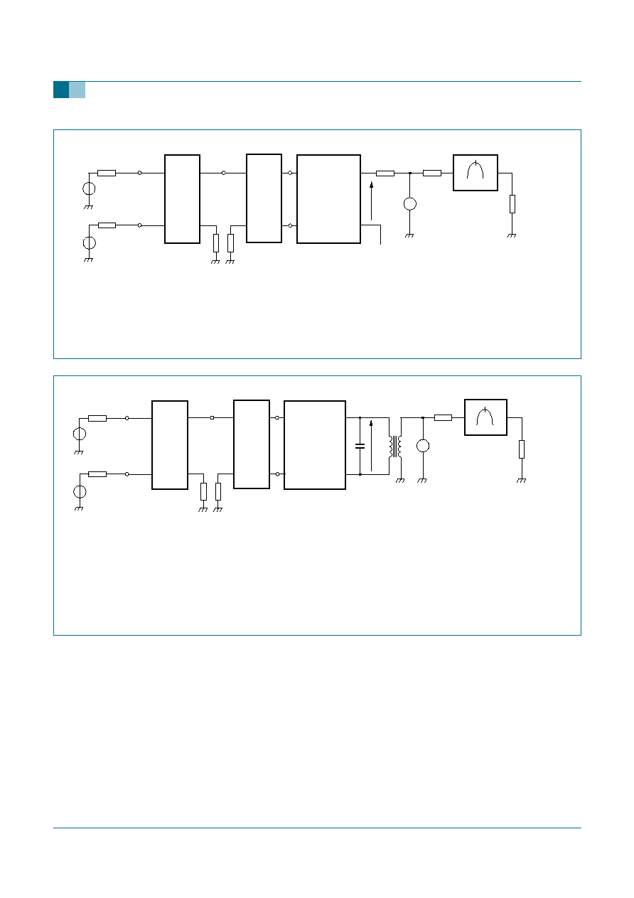
9397 750 14179
� Koninklijke Philips Electronics N.V. 2004. All rights reserved.
Product data sheet
Rev. 01 -- 14 December 2004
37 of 53
Philips Semiconductors
TDA6650ATT; TDA6651ATT
5 V mixer/oscillator and low noise PLL synthesizer
V
o
= V
meas
+ 3.75 dB.
Wanted signal source at f
RFpix
is 70 dB
�
V.
Unwanted output signal at f
snd
.
The level of unwanted signal is measured by causing 0.3 % AM modulation in the wanted signal.
Fig 23. Cross modulation measurement in high band with asymmetrical IF output
50
50
wanted
signal
source
unwanted
signal
source
AM = 30%
1 kHz
V
HBIN1
HBIN2
A
B
C
D
HYBRID
A
B
C
D
HYBRID
10 dB
attenuator
Vmeas
RMS
voltmeter
FILTER
DUT
57 MHz
50
50
e
u
e
w
IFOUTA
IFOUTB
V
CCA
001aac097
50
modulation
analyzer
27
V
o
V'
meas
= V
o
-
(transformer ratio N1/N2 = 5 and loss).
Wanted signal source at f
RFpix
is 70 dB
�
V.
The level of unwanted signal V
o
at f
snd
is measured by causing 0.3 % AM modulation in the wanted output signal.
N1 = 10 turns.
N2 = 2 turns.
N1/N2 = 5.
Fig 24. Cross modulation measurement in high band with symmetrical IF output
A
B
C
D
HYBRID
A
B
C
D
HYBRID
DUT
IFOUTA
IFOUTB
001aac098
C
N1
N2
transformer
V
FILTER
57 MHz
50
50
wanted
signal
source
unwanted
signal
source
AM = 30%
1 kHz
HBIN1
HBIN2
6 dB
attenuator
V'
meas
RMS
voltmeter
50
50
e
u
e
w
50
modulation
analyzer
V
o

9397 750 14179
� Koninklijke Philips Electronics N.V. 2004. All rights reserved.
Product data sheet
Rev. 01 -- 14 December 2004
38 of 53
Philips Semiconductors
TDA6650ATT; TDA6651ATT
5 V mixer/oscillator and low noise PLL synthesizer
The TDA6650ATT; TDA6651ATT PLL loop stability is guaranteed in the configuration of
the
Figure 27
to
Figure 30
. In this configuration, the external supply source is 30 V
minimum, the pull-up resistor, R19 is 15 k
and all of the local oscillators are aligned to
operate at a maximum tuning voltage of 26 V. If the configuration is changed, there might
be an impact on the loop stability.
For any other configurations, a stability analysis must be performed. The conventional PLL
AC model (cf. SIMPATA Philips software) used for the stability analysis, is valid provided
the external source (DC supply source or DC-to-DC converter) is able to deliver a
minimum current that is equal to the charge pump current in use.
Z
i
>> 50
V
i
= 2
�
V
meas
.
V
i
= V
meas
+ 6 dB.
Fig 25. Maximum RF input level without lock-out in low and mid band with asymmetrical
IF output
Loss in hybrid = 1 dB.
V
i
= V
meas
-
loss.
Fig 26. Maximum RF input level without lock-out in high band with asymmetrical IF output
fce755
50
50
50
V
e
V
meas
RMS
voltmeter
spectrum
analyzer
DUT
signal
source
LBIN
or
MBIN
IFOUTA
IFOUTB
V
CCA
27
fce756
V
DUT
A
B
e
C
D
HYBRID
HBIN1
HBIN2
IFOUTA
IFOUTB
V
CCA
50
50
50
50
V
meas
RMS
voltmeter
spectrum
analyzer
signal
source
27
V
i

9397 750 14179
� Koninklijke Philips Electronics N.V. 2004. All rights reserved.
Product data sheet
Rev. 01 -- 14 December 2004
39 of 53
Philips Semiconductors
TDA6650ATT; TDA6651ATT
5 V mixer/oscillator and low noise PLL synthesizer
The delivered current can be simply calculated with the following formula:
where:
I
delivered
is the delivered current.
V
DC
is the supply source voltage or DC-to-DC converter output voltage.
V
T
is the tuning voltage.
R
pu
is the pull-up resistor between the DC supply source (or the DC-to-DC converter
output) and the tuning line (R19 in
Figure 27
to
Figure 30
).
I
CP
is the charge pump current in use.
I
delivered
V
DC
V
T
�
R
pu
------------------------
I
CP
>
=

xxxxxxxxxxxxxxxxxxxxx xxxxxxxxxxxxxxxxxxxxxxxxxx xxxxxxx x x x xxxxxxxxxxxxxxxxxxxxxxxxxxxxxx xxxxxxxxxxxxxxxxxxx xx xx
xxxxx xxxxxxxxxxxxxxxxxxxxxxxxxxx xxxxxxxxxxxxxxxxxxx xxxxxx xxxxxxxxxxxxxxxxxxxxxxxxxxxxxxxxxxx xxxxxxxxxxxx x x
xxxxxxxxxxxxxxxxxxxxx xxxxxxxxxxxxxxxxxxxxxxxxxxxxxx xxxxx xxxxxxxxxxxxxxxxxxxxxxxxxxxxxxxxxxxxxxxxxxxxxxxxxx xxxxxxxx
xxxxxxxxxxxxxxxxxxxxxxxxx xxxxxxxxxxxxxxxxxxxx xxx
9397 750 14179
� K
oninklijk
e Philips Electronics N.V
. 2004. All r
ights reser
v
ed.
Pr
oduct data sheet
Re
v
.
01 -- 14 December 2004
40 of 53
Philips Semiconductor
s
TD
A6650A
TT
; TD
A6651A
TT
5 V mix
er/oscillator and lo
w noise PLL synthesiz
er
The pin numbers in parenthesis represent the TDA6651ATT.
Fig 27. Measurement circuit for digital application, with asymmetrical IF output and ISDB-T compliant loop filter
1 (38)
J4
LOW
C4
4.7
nF
HBIN1
1
L4
TOKO
500 nH
6
4
2
*
4t
3
2
2 (37)
HBIN2
3 (36)
MBIN
4 (35)
LBIN
5 (34)
RFGND
6 (33)
IFFIL1
7 (32)
IFFIL2
8 (31)
BS4
9 (30)
AGC
10 (29)
TDA6650ATT
(TDA6651ATT)
BS3
11 (28)
BS2
12 (27)
BS1
13 (26)
BVS
14 (25)
ADC/BS5
15 (24)
SCL
16 (23)
SDA
17 (22)
AS
18 (21)
1 2 3 4
5 V bus
J8
J7
SCL
SDA
AS
5 6
XTOUT
19 (20)
C19
C30
10
�
F
18 pF
Y1
4 MHz
XTAL1
(1) 38
LOSCIN
(2) 37
LOSCOUT
(3) 36
OSCGND
(4) 35
MOSCIN2
(5) 34
MOSCIN1
(6) 33
HOSCIN2
(7) 32
HOSCOUT2
(8) 31
HOSCOUT1
(9) 30
HOSCIN1
(10) 29
IFGND
(11) 28
IFOUTA
(12) 27
IFOUTB
(13) 26
(14) 25
PLLGND
(15) 24
V
CCD
V
CCA
(16) 23
CP
(17) 22
VT
(18) 21
n.c.
(19) 20
XTAL2
R20
C27
C28
150 nF
TP1
AGC
12 pF
D4
1 k
R21
D5
1 k
R22
D6
1 k
R23
D7
1 k
R24
ST2
ADC
VCC
D8
1 k
R14
R9
330
R10
330
R11
330
C29
4.7 nF
test
R27
3.3
k
R28
3.3
k
1 k
C26
12 pF
J3
MID
C3
4.7
nF
J1
HIGH1
C1
4.7
nF
J2
HIGH2
C2
4.7
nF
ST1
1 2 3 4
J5
5 V bus
30 V
V
CC
V
CC
5 V bus
V
CC
V
CC
30 V
J6
IF out
001aac099
C32
10
�
F
C31
10
�
F
L3
C7
1.5 pF
N750
C34
33 pF
N750
C33
33 pF
N750
8.2 pF
N470
3.9 nF
C11 1 pF
N750
C12 1 pF
N750
C13 1 pF
N750
C14 1 pF
N750
C6
1 pF
N750
C5
D1
L1
25 nH
L2
16 nH
R02255
D2
BB178
D3
BB179
BB182
15 pF
N750
R1
12
R3
5.6 k
R8
R7
1 k
R26
27
R19
15 k
5.6 k
R5
5.6 k
R2
5.6 k
R13
6.8 k
R4
5.6 k
R6
27
88 nH
R07254
C18
C17
C23
4.7 nF
C21
47 nF
C20
470 pF
C16
4.7 nF
C15
4.7 nF

xxxxxxxxxxxxxxxxxxxxx xxxxxxxxxxxxxxxxxxxxxxxxxx xxxxxxx x x x xxxxxxxxxxxxxxxxxxxxxxxxxxxxxx xxxxxxxxxxxxxxxxxxx xx xx
xxxxx xxxxxxxxxxxxxxxxxxxxxxxxxxx xxxxxxxxxxxxxxxxxxx xxxxxx xxxxxxxxxxxxxxxxxxxxxxxxxxxxxxxxxxx xxxxxxxxxxxx x x
xxxxxxxxxxxxxxxxxxxxx xxxxxxxxxxxxxxxxxxxxxxxxxxxxxx xxxxx xxxxxxxxxxxxxxxxxxxxxxxxxxxxxxxxxxxxxxxxxxxxxxxxxx xxxxxxxx
xxxxxxxxxxxxxxxxxxxxxxxxx xxxxxxxxxxxxxxxxxxxx xxx
9397 750 14179
� K
oninklijk
e Philips Electronics N.V
. 2004. All r
ights reser
v
ed.
Pr
oduct data sheet
Re
v
.
01 -- 14 December 2004
41 of 53
Philips Semiconductor
s
TD
A6650A
TT
; TD
A6651A
TT
5 V mix
er/oscillator and lo
w noise PLL synthesiz
er
The pin numbers in parenthesis represent the TDA6651ATT.
Fig 28. Measurement circuit for digital application, with symmetrical IF output and ISDB-T compliant loop filter
1 (38)
J4
LOW
C4
4.7
nF
HBIN1
1
L4
TOKO
500 nH
6
4
2
*
4t
3
2
2 (37)
HBIN2
3 (36)
MBIN
4 (35)
LBIN
5 (34)
RFGND
6 (33)
IFFIL1
7 (32)
IFFIL2
8 (31)
BS4
9 (30)
AGC
10 (29)
TDA6651ATT
BS3
11 (28)
BS2
12 (27)
BS1
13 (26)
BVS
14 (25)
ADC/BS5
15 (24)
SCL
16 (23)
SDA
17 (22)
AS
18 (21)
1 2 3 4
5 V bus
J8
J7
SCL
SDA
AS
5 6
XTOUT
19 (20)
C19
C30
10
�
F
18 pF
Y1
4 MHz
XTAL1
(1) 38
LOSCIN
(2) 37
LOSCOUT
(3) 36
OSCGND
(4) 35
MOSCIN2
(5) 34
MOSCIN1
(6) 33
HOSCIN2
(7) 32
HOSCOUT2
(8) 31
HOSCOUT1
(9) 30
HOSCIN1
(10) 29
IFGND
(11) 28
IFOUTA
(12) 27
IFOUTB
(13) 26
(14) 25
PLLGND
(15) 24
V
CCD
V
CCA
(16) 23
CP
(17) 22
VT
(18) 21
n.c.
(19) 20
XTAL2
R20
C27
C28
150 nF
TP1
AGC
12 pF
D4
1 k
R21
D5
1 k
R22
D6
1 k
R23
D7
1 k
R24
ST2
ADC
VCC
D8
1 k
R14
R9
330
R10
330
R11
330
C29
4.7 nF
test
R27
3.3
k
R28
3.3
k
1 k
C26
12 pF
J3
MID
C3
4.7
nF
J1
HIGH1
C1
4.7
nF
J2
HIGH2
C2
4.7
nF
ST1
1 2 3 4
J5
5 V bus
30 V
V
CC
V
CC
5 V bus
V
CC
30 V
J6
IF out
001aac100
C32
10
�
F
C31
10
�
F
L3
C7
1.5 pF
N750
C34
33 pF
N750
C33
33 pF
N750
8.2 pF
N470
3.9 nF
C11 1 pF
N750
C12 1 pF
N750
C13 1 pF
N750
C14 1 pF
N750
C6
1 pF
N750
C5
D1
L1
25 nH
L2
16 nH
R02255
D2
BB178
D3
BB179
BB182
15 pF
N750
R1
12
R3
5.6 k
R8
R7
1 k
R19
15 k
5.6 k
R5
5.6 k
R2
5.6 k
R13
6.8 k
R4
5.6 k
R6
27
88 nH
R07254
C18
C17
12 pF
C25
C24
4.7
nF
C23
4.7
nF
C21
47 nF
C20
470 pF
C16
4.7 nF
C15
4.7 nF
1
TR1
TOKO
7451
6
4
3
2

xxxxxxxxxxxxxxxxxxxxx xxxxxxxxxxxxxxxxxxxxxxxxxx xxxxxxx x x x xxxxxxxxxxxxxxxxxxxxxxxxxxxxxx xxxxxxxxxxxxxxxxxxx xx xx
xxxxx xxxxxxxxxxxxxxxxxxxxxxxxxxx xxxxxxxxxxxxxxxxxxx xxxxxx xxxxxxxxxxxxxxxxxxxxxxxxxxxxxxxxxxx xxxxxxxxxxxx x x
xxxxxxxxxxxxxxxxxxxxx xxxxxxxxxxxxxxxxxxxxxxxxxxxxxx xxxxx xxxxxxxxxxxxxxxxxxxxxxxxxxxxxxxxxxxxxxxxxxxxxxxxxx xxxxxxxx
xxxxxxxxxxxxxxxxxxxxxxxxx xxxxxxxxxxxxxxxxxxxx xxx
9397 750 14179
� K
oninklijk
e Philips Electronics N.V
. 2004. All r
ights reser
v
ed.
Pr
oduct data sheet
Re
v
.
01 -- 14 December 2004
42 of 53
Philips Semiconductor
s
TD
A6650A
TT
; TD
A6651A
TT
5 V mix
er/oscillator and lo
w noise PLL synthesiz
er
The pin numbers in parenthesis represent the TDA6651ATT.
Fig 29. Measurement circuit for hybrid application, with asymmetrical IF output and loop filter for NTSC-Japan and ISDB-T standards
1 (38)
J4
LOW
C4
4.7
nF
HBIN1
1
L4
TOKO
500 nH
6
4
2
*
4t
3
2
2 (37)
HBIN2
3 (36)
MBIN
4 (35)
LBIN
5 (34)
RFGND
6 (33)
IFFIL1
7 (32)
IFFIL2
8 (31)
BS4
9 (30)
AGC
10 (29)
TDA6650ATT
(TDA6651ATT)
BS3
11 (28)
BS2
12 (27)
BS1
13 (26)
BVS
14 (25)
ADC/BS5
15 (24)
SCL
16 (23)
SDA
17 (22)
AS
18 (21)
1 2 3 4
5 V bus
J8
J7
SCL
SDA
AS
5 6
XTOUT
19 (20)
C19
C30
10
�
F
18 pF
Y1
4 MHz
XTAL1
(1) 38
LOSCIN
(2) 37
LOSCOUT
(3) 36
OSCGND
(4) 35
MOSCIN2
(5) 34
MOSCIN1
(6) 33
HOSCIN2
(7) 32
HOSCOUT2
(8) 31
HOSCOUT1
(9) 30
HOSCIN1
(10) 29
IFGND
(11) 28
IFOUTA
(12) 27
IFOUTB
(13) 26
(14) 25
PLLGND
(15) 24
V
CCD
V
CCA
(16) 23
CP
(17) 22
VT
(18) 21
n.c.
(19) 20
XTAL2
R20
C27
C28
150 nF
TP1
AGC
12 pF
D4
1 k
R21
D5
1 k
R22
D6
1 k
R23
D7
1 k
R24
ST2
ADC
VCC
D8
1 k
R14
R9
330
R10
330
R11
330
C29
4.7 nF
test
R27
3.3
k
R28
3.3
k
1 k
C26
12 pF
J3
MID
C3
4.7
nF
J1
HIGH1
C1
4.7
nF
J2
HIGH2
C2
4.7
nF
ST1
1 2 3 4
J5
5 V bus
30 V
V
CC
V
CC
5 V bus
V
CC
V
CC
30 V
J6
IF out
001aac044
C32
10
�
F
C31
10
�
F
L3
C7
1.5 pF
N750
C34
33 pF
N750
C33
33 pF
N750
8.2 pF
N470
4.7 nF
C11 1 pF
N750
C12 1 pF
N750
C13 1 pF
N750
C14 1 pF
N750
C6
1 pF
N750
C5
D1
L1
25 nH
L2
16 nH
R02255
D2
BB178
D3
BB179
BB182
15 pF
N750
R1
12
R3
5.6 k
R8
R7
1 k
R26
27
R19
15 k
5.6 k
R5
5.6 k
R2
5.6 k
R13
1.8 k
R4
5.6 k
R6
27
88 nH
R07254
C18
C17
C23
4.7 nF
C21
100 nF
C20
2.7 nF
C16
4.7 nF
C15
4.7 nF

xxxxxxxxxxxxxxxxxxxxx xxxxxxxxxxxxxxxxxxxxxxxxxx xxxxxxx x x x xxxxxxxxxxxxxxxxxxxxxxxxxxxxxx xxxxxxxxxxxxxxxxxxx xx xx
xxxxx xxxxxxxxxxxxxxxxxxxxxxxxxxx xxxxxxxxxxxxxxxxxxx xxxxxx xxxxxxxxxxxxxxxxxxxxxxxxxxxxxxxxxxx xxxxxxxxxxxx x x
xxxxxxxxxxxxxxxxxxxxx xxxxxxxxxxxxxxxxxxxxxxxxxxxxxx xxxxx xxxxxxxxxxxxxxxxxxxxxxxxxxxxxxxxxxxxxxxxxxxxxxxxxx xxxxxxxx
xxxxxxxxxxxxxxxxxxxxxxxxx xxxxxxxxxxxxxxxxxxxx xxx
9397 750 14179
� K
oninklijk
e Philips Electronics N.V
. 2004. All r
ights reser
v
ed.
Pr
oduct data sheet
Re
v
.
01 -- 14 December 2004
43 of 53
Philips Semiconductor
s
TD
A6650A
TT
; TD
A6651A
TT
5 V mix
er/oscillator and lo
w noise PLL synthesiz
er
The pin numbers in parenthesis represent the TDA6651ATT.
Fig 30. Measurement circuit for hybrid application, with symmetrical IF output and loop filter for NTSC-Japan and ISDB-T standards
1 (38)
J4
LOW
C4
4.7
nF
HBIN1
1
L4
TOKO
500 nH
6
4
2
*
4t
3
2
2 (37)
HBIN2
3 (36)
MBIN
4 (35)
LBIN
5 (34)
RFGND
6 (33)
IFFIL1
7 (32)
IFFIL2
8 (31)
BS4
9 (30)
AGC
10 (29)
TDA6651ATT
BS3
11 (28)
BS2
12 (27)
BS1
13 (26)
BVS
14 (25)
ADC/BS5
15 (24)
SCL
16 (23)
SDA
17 (22)
AS
18 (21)
1 2 3 4
5 V bus
J8
J7
SCL
SDA
AS
5 6
XTOUT
19 (20)
C19
C30
10
�
F
18 pF
Y1
4 MHz
XTAL1
(1) 38
LOSCIN
(2) 37
LOSCOUT
(3) 36
OSCGND
(4) 35
MOSCIN2
(5) 34
MOSCIN1
(6) 33
HOSCIN2
(7) 32
HOSCOUT2
(8) 31
HOSCOUT1
(9) 30
HOSCIN1
(10) 29
IFGND
(11) 28
IFOUTA
(12) 27
IFOUTB
(13) 26
(14) 25
PLLGND
(15) 24
V
CCD
V
CCA
(16) 23
CP
(17) 22
VT
(18) 21
n.c.
(19) 20
XTAL2
R20
C27
C28
150 nF
TP1
AGC
12 pF
D4
1 k
R21
D5
1 k
R22
D6
1 k
R23
D7
1 k
R24
ST2
ADC
VCC
D8
1 k
R14
R9
330
R10
330
R11
330
C29
4.7 nF
test
R27
3.3
k
R28
3.3
k
1 k
C26
12 pF
J3
MID
C3
4.7
nF
J1
HIGH1
C1
4.7
nF
J2
HIGH2
C2
4.7
nF
ST1
1 2 3 4
J5
5 V bus
30 V
V
CC
V
CC
5 V bus
V
CC
30 V
J6
IF out
001aac101
C32
10
�
F
C31
10
�
F
L3
C7
1.5 pF
N750
C34
33 pF
N750
C33
33 pF
N750
8.2 pF
N470
4.7 nF
C11 1 pF
N750
C12 1 pF
N750
C13 1 pF
N750
C14 1 pF
N750
C6
1 pF
N750
C5
D1
L1
25 nH
L2
16 nH
R02255
D2
BB178
D3
BB179
BB182
15 pF
N750
R1
12
R3
5.6 k
R8
R7
1 k
R19
15 k
5.6 k
R5
5.6 k
R2
5.6 k
R13
1.8 k
R4
5.6 k
R6
27
88 nH
R07254
C18
C17
12 pF
C25
C24
4.7
nF
C23
4.7
nF
C21
100 nF
C20
2.7 nF
C16
4.7 nF
C15
4.7 nF
1
TR1
TOKO
7451
6
4
3
2

9397 750 14179
� Koninklijke Philips Electronics N.V. 2004. All rights reserved.
Product data sheet
Rev. 01 -- 14 December 2004
44 of 53
Philips Semiconductors
TDA6650ATT; TDA6651ATT
5 V mixer/oscillator and low noise PLL synthesizer
13. Application information
13.1 Tuning amplifier
The tuning amplifier is capable of driving the varicap voltage without an external transistor.
The tuning voltage output must be connected to an external load of 15 k
which is
connected to the tuning voltage supply rail. The loop filter design depends on the oscillator
characteristics and the selected reference frequency as well as the required PLL loop
bandwidth.
Applications with the TDA6650ATT; TDA6651ATT have a large loop bandwidth, in the
order of a few tens of kHz. The calculation of the loop filter elements has to be done for
each application, it depends on the reference frequency and charge pump current. A
simulation of the loop can easily be done using the SIMPATA software from Philips.
13.2 Crystal oscillator
The TDA6650ATT; TDA6651ATT needs to be used with a 4 MHz crystal in series with a
capacitor with a typical value of 18 pF, connected between pin XTAL1 and pin XTAL2.
Philips crystal 4322 143 04093 is recommended. When choosing a crystal, take care to
select a crystal able to withstand the drive level of the TDA6650ATT; TDA6651ATT without
suffering from accelerated ageing. For optimum performances, it is highly recommended
to connect the 4 MHz crystal without any serial resistance.
The crystal oscillator of the TDA6650ATT; TDA6651ATT should not be driven (forced)
from an external signal. Do not use the signal on pins XTAL1 or XTAL2, or the signal
present on the crystal, to drive an external IC or for any other use as this may dramatically
degrade the phase noise performance of the TDA6650ATT; TDA6651ATT.
13.3 Examples of I
2
C-bus program sequences
Table 20
to
Table 25
show various sequences where:
S = START
A = acknowledge
P = STOP.
The following conditions apply:
LO frequency is 800 MHz
f
comp
= 142.86 kHz
N = 5600
BS3 output port is on and all other ports are off: thus the high band is selected
Charge pump current I
CP
= 600
�
A
Normal mode, with XTOUT buffer on
I
AGC
= 220 nA
AGC take-over point is set to 112 dB
�
V (p-p)
Address selection is adjusted to make address C2 valid.

9397 750 14179
� Koninklijke Philips Electronics N.V. 2004. All rights reserved.
Product data sheet
Rev. 01 -- 14 December 2004
45 of 53
Philips Semiconductors
TDA6650ATT; TDA6651ATT
5 V mixer/oscillator and low noise PLL synthesizer
To fully program the device, either sequence of
Table 20
or
Table 21
can be used, while
other arrangements of the bytes are also possible.
[1]
Control byte 1 with bit T/A = 1, to program test bits T2, T1 and T0 and reference divider ratio bits R2, R1
and R0.
[2]
Control byte 1 with bit T/A = 0, to program AGC time constant bit ATC and AGC take-over point bits
AL2, AL1 and AL0.
[1]
Control byte 1 with bit T/A = 1, to program test bits T2, T1 and T0 and reference divider ratio bits R2, R1
and R0.
[2]
Control byte 1 with bit T/A = 0, to program AGC time constant bit ATC and AGC take-over point bits
AL2, AL1 and AL0.
[1]
Control byte 1 with bit T/A = 1, to program test bits T2, T1 and T0 and reference divider ratio bits R2, R1
and R0.
[1]
Control byte 1 with bit T/A = 1, to program test bits T2, T1 and T0 and reference divider ratio bits R2, R1
and R0.
[1]
Control byte 1 with bit T/A = 0, to program AGC time constant bit ATC and AGC take-over point bits
AL2, AL1 and AL0.
Table 20:
Complete sequence 1
Start
Address
byte
Divider
byte 1
Divider
byte 2
Control
byte 1
[1]
Control
byte 2
Control
byte 1
[2]
Stop
S
C2
A
15
A
E0
A
C9
A
E4
A
84
A
P
Table 21:
Complete sequence 2
Start
Address
byte
Control
byte 1
[1]
Control
byte 2
Divider
byte 1
Divider
byte 2
Control
byte 1
[2]
Stop
S
C2
A
C9
A
E4
A
15
A
E0
A
84
A
P
Table 22:
Sequence to program only the main divider ratio
Start
Address byte
Divider byte 1
Divider byte 2
Stop
S
C2
A
15
A
E0
A
P
Table 23:
Sequence to change the charge pump current, the ports and the test mode. If the
reference divider ratio is changed, it is necessary to send the DB1 and DB2 bytes
Start
Address byte
Control byte 1
[1]
Control byte 2
Stop
S
C2
A
C9
A
E4
A
P
Table 24:
Sequence to change the test mode. If the reference divider ratio is changed, it is
necessary to send the DB1 and DB2 bytes
Start
Address byte
Control byte 1
[1]
Stop
S
C2
A
C9
A
P
Table 25:
Sequence to change the charge pump current, the ports and the AGC data
Start
Address byte
Control byte 1
[1]
Control byte 2
Stop
S
C2
A
82
A
E4
A
P

9397 750 14179
� Koninklijke Philips Electronics N.V. 2004. All rights reserved.
Product data sheet
Rev. 01 -- 14 December 2004
46 of 53
Philips Semiconductors
TDA6650ATT; TDA6651ATT
5 V mixer/oscillator and low noise PLL synthesizer
[1]
Control byte 1 with bit T/A = 0, to program AGC time constant bit ATC and AGC take-over point bits
AL2, AL1 and AL0.
Table 26:
Sequence to change only the AGC data
Start
Address byte
Control byte 1
[1]
Stop
S
C2
A
84
A
P

9397 750 14179
� Koninklijke Philips Electronics N.V. 2004. All rights reserved.
Product data sheet
Rev. 01 -- 14 December 2004
47 of 53
Philips Semiconductors
TDA6650ATT; TDA6651ATT
5 V mixer/oscillator and low noise PLL synthesizer
14. Package outline
Fig 31. Package outline SOT510-1 (TSSOP38)
UNIT
A
1
A
2
A
3
b
p
c
D
(1)
E
(2)
e
H
E
L
L
p
Z
(1)
y
w
v
REFERENCES
OUTLINE
VERSION
EUROPEAN
PROJECTION
ISSUE DATE
IEC
JEDEC
JEITA
mm
0.15
0.05
8
0
o
o
0.08
DIMENSIONS (mm are the original dimensions).
Notes
1. Plastic or metal protrusions of 0.15 mm maximum per side are not included.
2. Plastic interlead protrusions of 0.25 mm maximum per side are not included.
SOT510-1
98-09-16
03-02-18
w
M
A
A
1
A
2
D
L
p
detail X
E
Z
e
c
L
X
(A )
3
0.25
1
19
38
20
y
b
H
0.95
0.85
0.27
0.17
0.20
0.09
9.8
9.6
4.5
4.3
0.5
1
0.2
6.4
0.49
0.21
0.08
0.7
0.5
p
E
v
M
A
A
TSSOP38: plastic thin shrink small outline package; 38 leads; body width 4.4 mm;
lead pitch 0.5 mm
SOT510-1
A
max.
1.1
0
2.5
5 mm
scale
pin 1 index

9397 750 14179
� Koninklijke Philips Electronics N.V. 2004. All rights reserved.
Product data sheet
Rev. 01 -- 14 December 2004
48 of 53
Philips Semiconductors
TDA6650ATT; TDA6651ATT
5 V mixer/oscillator and low noise PLL synthesizer
15. Handling information
Inputs and outputs are protected against electrostatic discharge in normal handling.
However, to be completely safe, it is desirable to take normal precautions appropriate to
handling integrated circuits.
16. Soldering
16.1 Introduction to soldering surface mount packages
This text gives a very brief insight to a complex technology. A more in-depth account of
soldering ICs can be found in our
Data Handbook IC26; Integrated Circuit Packages
(document order number 9398 652 90011).
There is no soldering method that is ideal for all surface mount IC packages. Wave
soldering can still be used for certain surface mount ICs, but it is not suitable for fine pitch
SMDs. In these situations reflow soldering is recommended.
16.2 Reflow soldering
Reflow soldering requires solder paste (a suspension of fine solder particles, flux and
binding agent) to be applied to the printed-circuit board by screen printing, stencilling or
pressure-syringe dispensing before package placement. Driven by legislation and
environmental forces the worldwide use of lead-free solder pastes is increasing.
Several methods exist for reflowing; for example, convection or convection/infrared
heating in a conveyor type oven. Throughput times (preheating, soldering and cooling)
vary between 100 seconds and 200 seconds depending on heating method.
Typical reflow peak temperatures range from 215
�
C to 270
�
C depending on solder paste
material. The top-surface temperature of the packages should preferably be kept:
�
below 225
�
C (SnPb process) or below 245
�
C (Pb-free process)
� for all BGA, HTSSON..T and SSOP..T packages
� for packages with a thickness
2.5 mm
� for packages with a thickness < 2.5 mm and a volume
350 mm
3
so called
thick/large packages.
�
below 240
�
C (SnPb process) or below 260
�
C (Pb-free process) for packages with a
thickness < 2.5 mm and a volume < 350 mm
3
so called small/thin packages.
Moisture sensitivity precautions, as indicated on packing, must be respected at all times.
16.3 Wave soldering
Conventional single wave soldering is not recommended for surface mount devices
(SMDs) or printed-circuit boards with a high component density, as solder bridging and
non-wetting can present major problems.
To overcome these problems the double-wave soldering method was specifically
developed.
If wave soldering is used the following conditions must be observed for optimal results:
9397 750 14179
� Koninklijke Philips Electronics N.V. 2004. All rights reserved.
Product data sheet
Rev. 01 -- 14 December 2004
49 of 53
Philips Semiconductors
TDA6650ATT; TDA6651ATT
5 V mixer/oscillator and low noise PLL synthesizer
�
Use a double-wave soldering method comprising a turbulent wave with high upward
pressure followed by a smooth laminar wave.
�
For packages with leads on two sides and a pitch (e):
� larger than or equal to 1.27 mm, the footprint longitudinal axis is preferred to be
parallel to the transport direction of the printed-circuit board;
� smaller than 1.27 mm, the footprint longitudinal axis must be parallel to the
transport direction of the printed-circuit board.
The footprint must incorporate solder thieves at the downstream end.
�
For packages with leads on four sides, the footprint must be placed at a 45
�
angle to
the transport direction of the printed-circuit board. The footprint must incorporate
solder thieves downstream and at the side corners.
During placement and before soldering, the package must be fixed with a droplet of
adhesive. The adhesive can be applied by screen printing, pin transfer or syringe
dispensing. The package can be soldered after the adhesive is cured.
Typical dwell time of the leads in the wave ranges from 3 seconds to 4 seconds at 250
�
C
or 265
�
C, depending on solder material applied, SnPb or Pb-free respectively.
A mildly-activated flux will eliminate the need for removal of corrosive residues in most
applications.
16.4 Manual soldering
Fix the component by first soldering two diagonally-opposite end leads. Use a low voltage
(24 V or less) soldering iron applied to the flat part of the lead. Contact time must be
limited to 10 seconds at up to 300
�
C.
When using a dedicated tool, all other leads can be soldered in one operation within
2 seconds to 5 seconds between 270
�
C and 320
�
C.
16.5 Package related soldering information
[1]
For more detailed information on the BGA packages refer to the
(LF)BGA Application Note (AN01026);
order a copy from your Philips Semiconductors sales office.
Table 27:
Suitability of surface mount IC packages for wave and reflow soldering methods
Package
[1]
Soldering method
Wave
Reflow
[2]
BGA, HTSSON..T
[3]
, LBGA, LFBGA, SQFP,
SSOP..T
[3]
, TFBGA, VFBGA, XSON
not suitable
suitable
DHVQFN, HBCC, HBGA, HLQFP, HSO, HSOP,
HSQFP, HSSON, HTQFP, HTSSOP, HVQFN,
HVSON, SMS
not suitable
[4]
suitable
PLCC
[5]
, SO, SOJ
suitable
suitable
LQFP, QFP, TQFP
not recommended
[5] [6]
suitable
SSOP, TSSOP, VSO, VSSOP
not recommended
[7]
suitable
CWQCCN..L
[8]
, PMFP
[9]
, WQCCN..L
[8]
not suitable
not suitable

9397 750 14179
� Koninklijke Philips Electronics N.V. 2004. All rights reserved.
Product data sheet
Rev. 01 -- 14 December 2004
50 of 53
Philips Semiconductors
TDA6650ATT; TDA6651ATT
5 V mixer/oscillator and low noise PLL synthesizer
[2]
All surface mount (SMD) packages are moisture sensitive. Depending upon the moisture content, the
maximum temperature (with respect to time) and body size of the package, there is a risk that internal or
external package cracks may occur due to vaporization of the moisture in them (the so called popcorn
effect). For details, refer to the Drypack information in the
Data Handbook IC26; Integrated Circuit
Packages; Section: Packing Methods.
[3]
These transparent plastic packages are extremely sensitive to reflow soldering conditions and must on no
account be processed through more than one soldering cycle or subjected to infrared reflow soldering with
peak temperature exceeding 217
�
C
�
10
�
C measured in the atmosphere of the reflow oven. The package
body peak temperature must be kept as low as possible.
[4]
These packages are not suitable for wave soldering. On versions with the heatsink on the bottom side, the
solder cannot penetrate between the printed-circuit board and the heatsink. On versions with the heatsink
on the top side, the solder might be deposited on the heatsink surface.
[5]
If wave soldering is considered, then the package must be placed at a 45
�
angle to the solder wave
direction. The package footprint must incorporate solder thieves downstream and at the side corners.
[6]
Wave soldering is suitable for LQFP, QFP and TQFP packages with a pitch (e) larger than 0.8 mm; it is
definitely not suitable for packages with a pitch (e) equal to or smaller than 0.65 mm.
[7]
Wave soldering is suitable for SSOP, TSSOP, VSO and VSSOP packages with a pitch (e) equal to or larger
than 0.65 mm; it is definitely not suitable for packages with a pitch (e) equal to or smaller than 0.5 mm.
[8]
Image sensor packages in principle should not be soldered. They are mounted in sockets or delivered
pre-mounted on flex foil. However, the image sensor package can be mounted by the client on a flex foil by
using a hot bar soldering process. The appropriate soldering profile can be provided on request.
[9]
Hot bar soldering or manual soldering is suitable for PMFP packages.

9397 750 14179
� Koninklijke Philips Electronics N.V. 2004. All rights reserved.
Product data sheet
Rev. 01 -- 14 December 2004
51 of 53
Philips Semiconductors
TDA6650ATT; TDA6651ATT
5 V mixer/oscillator and low noise PLL synthesizer
17. Revision history
Table 28:
Revision history
Document ID
Release
date
Data sheet status
Change
notice
Doc. number
Supersedes
TDA6650ATT_6651ATT_1
20041214
Product data sheet
-
9397 750 14179
-

Philips Semiconductors
TDA6650ATT; TDA6651ATT
5 V mixer/oscillator and low noise PLL synthesizer
9397 750 14179
� Koninklijke Philips Electronics N.V. 2004. All rights reserved.
Product data sheet
Rev. 01 -- 14 December 2004
52 of 53
18. Data sheet status
[1]
Please consult the most recently issued data sheet before initiating or completing a design.
[2]
The product status of the device(s) described in this data sheet may have changed since this data sheet was published. The latest information is available on the Internet at
URL http://www.semiconductors.philips.com.
[3]
For data sheets describing multiple type numbers, the highest-level product status determines the data sheet status.
19. Definitions
Short-form specification -- The data in a short-form specification is
extracted from a full data sheet with the same type number and title. For
detailed information see the relevant data sheet or data handbook.
Limiting values definition -- Limiting values given are in accordance with
the Absolute Maximum Rating System (IEC 60134). Stress above one or
more of the limiting values may cause permanent damage to the device.
These are stress ratings only and operation of the device at these or at any
other conditions above those given in the Characteristics sections of the
specification is not implied. Exposure to limiting values for extended periods
may affect device reliability.
Application information -- Applications that are described herein for any
of these products are for illustrative purposes only. Philips Semiconductors
make no representation or warranty that such applications will be suitable for
the specified use without further testing or modification.
20. Disclaimers
Life support -- These products are not designed for use in life support
appliances, devices, or systems where malfunction of these products can
reasonably be expected to result in personal injury. Philips Semiconductors
customers using or selling these products for use in such applications do so
at their own risk and agree to fully indemnify Philips Semiconductors for any
damages resulting from such application.
Right to make changes -- Philips Semiconductors reserves the right to
make changes in the products - including circuits, standard cells, and/or
software - described or contained herein in order to improve design and/or
performance. When the product is in full production (status `Production'),
relevant changes will be communicated via a Customer Product/Process
Change Notification (CPCN). Philips Semiconductors assumes no
responsibility or liability for the use of any of these products, conveys no
license or title under any patent, copyright, or mask work right to these
products, and makes no representations or warranties that these products are
free from patent, copyright, or mask work right infringement, unless otherwise
specified.
21. Licenses
22. Contact information
For additional information, please visit: http://www.semiconductors.philips.com
For sales office addresses, send an email to: sales.addresses@www.semiconductors.philips.com
Level
Data sheet status
[1]
Product status
[2] [3]
Definition
I
Objective data
Development
This data sheet contains data from the objective specification for product development. Philips
Semiconductors reserves the right to change the specification in any manner without notice.
II
Preliminary data
Qualification
This data sheet contains data from the preliminary specification. Supplementary data will be published
at a later date. Philips Semiconductors reserves the right to change the specification without notice, in
order to improve the design and supply the best possible product.
III
Product data
Production
This data sheet contains data from the product specification. Philips Semiconductors reserves the
right to make changes at any time in order to improve the design, manufacturing and supply. Relevant
changes will be communicated via a Customer Product/Process Change Notification (CPCN).
Purchase of Philips I
2
C-bus components
Purchase of Philips I
2
C-bus components conveys a
license under the Philips' I
2
C-bus patent to use the
components in the I
2
C-bus system provided the system
conforms to the I
2
C-bus specification defined by
Koninklijke Philips Electronics N.V. This specification
can be ordered using the code 9398 393 40011.

� Koninklijke Philips Electronics N.V. 2004
All rights are reserved. Reproduction in whole or in part is prohibited without the prior
written consent of the copyright owner. The information presented in this document does
not form part of any quotation or contract, is believed to be accurate and reliable and may
be changed without notice. No liability will be accepted by the publisher for any
consequence of its use. Publication thereof does not convey nor imply any license under
patent- or other industrial or intellectual property rights.
Date of release: 14 December 2004
Document number: 9397 750 14179
Published in The Netherlands
Philips Semiconductors
TDA6650ATT; TDA6651ATT
5 V mixer/oscillator and low noise PLL synthesizer
23. Contents
1
General description . . . . . . . . . . . . . . . . . . . . . . 1
2
Features . . . . . . . . . . . . . . . . . . . . . . . . . . . . . . . 2
3
Applications . . . . . . . . . . . . . . . . . . . . . . . . . . . . 3
3.1
Application summary . . . . . . . . . . . . . . . . . . . . 3
4
Ordering information . . . . . . . . . . . . . . . . . . . . . 3
5
Block diagram . . . . . . . . . . . . . . . . . . . . . . . . . . 4
6
Pinning information . . . . . . . . . . . . . . . . . . . . . . 5
6.1
Pin description . . . . . . . . . . . . . . . . . . . . . . . . . 5
6.2
Pinning . . . . . . . . . . . . . . . . . . . . . . . . . . . . . . . 6
7
Functional description . . . . . . . . . . . . . . . . . . . 6
7.1
Mixer, oscillator and PLL (MOPLL) functions . . 6
7.2
I
2
C-bus voltage . . . . . . . . . . . . . . . . . . . . . . . . . 7
7.3
Phase noise, I
2
C-bus traffic and crosstalk . . . . 7
8
I
2
C-bus protocol . . . . . . . . . . . . . . . . . . . . . . . . . 8
8.1
Write mode; R/W = 0 . . . . . . . . . . . . . . . . . . . . 8
8.1.1
I
2
C-bus address selection. . . . . . . . . . . . . . . . 10
8.1.2
XTOUT output buffer and mode setting . . . . . 10
8.1.3
Step frequency setting . . . . . . . . . . . . . . . . . . 10
8.1.4
AGC detector setting . . . . . . . . . . . . . . . . . . . 11
8.1.5
Charge pump current setting . . . . . . . . . . . . . 11
8.2
Read mode; R/W = 1 . . . . . . . . . . . . . . . . . . . 12
8.3
Status at power-on reset. . . . . . . . . . . . . . . . . 13
9
Internal circuitry. . . . . . . . . . . . . . . . . . . . . . . . 14
10
Limiting values. . . . . . . . . . . . . . . . . . . . . . . . . 18
11
Thermal characteristics. . . . . . . . . . . . . . . . . . 19
12
Characteristics . . . . . . . . . . . . . . . . . . . . . . . . . 20
13
Application information. . . . . . . . . . . . . . . . . . 44
13.1
Tuning amplifier. . . . . . . . . . . . . . . . . . . . . . . . 44
13.2
Crystal oscillator . . . . . . . . . . . . . . . . . . . . . . . 44
13.3
Examples of I
2
C-bus program sequences . . . 44
14
Package outline . . . . . . . . . . . . . . . . . . . . . . . . 47
15
Handling information. . . . . . . . . . . . . . . . . . . . 48
16
Soldering . . . . . . . . . . . . . . . . . . . . . . . . . . . . . 48
16.1
Introduction to soldering surface mount
packages . . . . . . . . . . . . . . . . . . . . . . . . . . . . 48
16.2
Reflow soldering . . . . . . . . . . . . . . . . . . . . . . . 48
16.3
Wave soldering . . . . . . . . . . . . . . . . . . . . . . . . 48
16.4
Manual soldering . . . . . . . . . . . . . . . . . . . . . . 49
16.5
Package related soldering information . . . . . . 49
17
Revision history . . . . . . . . . . . . . . . . . . . . . . . . 51
18
Data sheet status . . . . . . . . . . . . . . . . . . . . . . . 52
19
Definitions . . . . . . . . . . . . . . . . . . . . . . . . . . . . 52
20
Disclaimers . . . . . . . . . . . . . . . . . . . . . . . . . . . . 52
21
Licenses . . . . . . . . . . . . . . . . . . . . . . . . . . . . . . 52
22
Contact information . . . . . . . . . . . . . . . . . . . . 52