Document Outline
- FEATURES
- APPLICATIONS
- GENERAL DESCRIPTION
- ORDERING INFORMATION
- QUICK REFERENCE DATA
- BLOCK DIAGRAM
- PINNING
- FUNCTIONAL DESCRIPTION
- Power supply
- Voltage supervisor
- State diagram
- LIMITING VALUES
- HANDLING
- THERMAL CHARACTERISTICS
- CHARACTERISTICS
- INTERNAL PIN CONFIGURATION
- APPLICATION INFORMATION
- PACKAGE OUTLINES
- SOLDERING
- DEFINITIONS
- LIFE SUPPORT APPLICATIONS
DATA SHEET
Product specification
Supersedes data of 1995 Feb 01
File under Integrated Circuits, IC02
1996 Dec 12
INTEGRATED CIRCUITS
TDA8001
Smart card interface

1996 Dec 12
2
Philips Semiconductors
Product specification
Smart card interface
TDA8001
FEATURES
∑
Protected I/O line
∑
V
CC
regulation (5 V
±
5%, 100 mA max. with controlled
rise and fall times)
∑
V
PP
generation (12.5, 15 or 21 V
±
2.5%, 50 mA max.,
with controlled rise and fall times) (only at TDA8001 and
TDA8001T)
∑
Clock generation (up to 10 MHz), with synchronous
frequency doubling
∑
Overload, thermal and card extraction protections
∑
Current limitation in case of short-circuit
∑
Idle mode and special circuitry for spikes killing during
powering on and off
∑
Two voltage supervisors (digital and analog supplies)
∑
Automatic activation and deactivation sequences
through an independent internal clock
∑
Enhanced ESD protections on card side (4 kV min.)
∑
Easy chaining for multiple card readers
∑
ISO 7816 compatibility.
APPLICATIONS
∑
Pay TV (multistandards conditional access system,
videoguard, newscript)
∑
Multi-application smart card readers (banking, vending
machine, electronic payment identification).
GENERAL DESCRIPTION
The TDA8001 is a complete, low-cost analog interface
which can be positioned between an asynchronous smart
card (ISO 7816) and a microcontroller. It is directly
compatible with the new Datacom chip verifier.
The complete supply, protection and control functions are
realized with only a few external components, making this
product very attractive for consumer applications
(see Chapter "Application information").
ORDERING INFORMATION
TYPE
NUMBER
PACKAGE
NAME
DESCRIPTION
VERSION
TDA8001;
TDA8001A
DIP28
plastic dual in-line package; 28 leads (600 mil)
SOT117-1
TDA8001T;
TDA8001AT
SO28
plastic small outline package; 28 leads; body width 7.5 mm
SOT136-1
1996 Dec 12
3
Philips Semiconductors
Product specification
Smart card interface
TDA8001
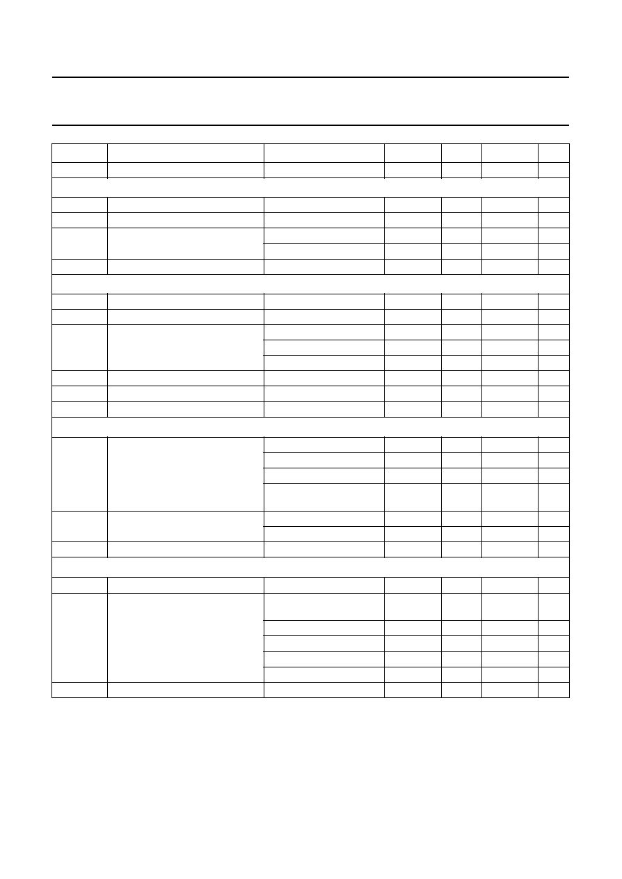
QUICK REFERENCE DATA
SYMBOL
PARAMETER
CONDITIONS
MIN.
TYP.
MAX.
UNIT
V
DD
supply voltage
6.7
-
18
V
I
DD
supply current
idle mode; V
DD
= 12 V
-
32
-
mA
active modes; unloaded
-
45
-
mA
V
th2
threshold voltage on V
SUP
4.5
-
4.72
V
V
th4
threshold voltage on V
DD
6
-
6.5
V
V
CC
card supply voltage
including static and dynamic
loads on 100 nF capacitor
4.75
5.0
5.25
V
I
CC
card supply current
operating
-
-
-
100
mA
detection
-
-
150
-
mA
limitation
-
-
-
200
mA
V
H
high voltage supply for
V
PP
-
-
30
V
V
PP
card programming
voltage (only at TDA8001
and TDA8001T)
(P = 5, 12.5, 15 and 21 V)
including static and dynamic
loads on 100 nF capacitor
P
-
2.5%
-
P + 2.5% V
I
PP
programming current
(read or write mode)
operating
-
-
-
50
mA
detection
-
-
75
-
mA
limitation
-
-
-
100
mA
SR
slew rate on V
CC
and V
PP
(rise and fall)
maximum load capacitor 150 nF
-
0.38
-
V/
µ
s
t
de
deactivation cycle duration
75
100
125
µ
s
f
clk
clock frequency
0
-
8
MHz
P
tot
continuous total power
dissipation
TDA8001; T
amb
= +70
∞
C;
see Fig.10
-
-
0.92
W
TDA8001T; T
amb
= +70
∞
C;
see Fig.11
-
-
2
W
T
amb
operating ambient
temperature
0
-
+70
∞
C
1996 Dec 12
4
Philips Semiconductors
Product specification
Smart card interface
TDA8001
BLOCK DIAGRAM
Fig.1 Block diagram.
handbook, full pagewidth
MBH813
PROTECTIONS
AND
ENABLE
MAIN
SUPPLY
VOLTAGE
SUPERVISOR
INTERNAL
CLOCK
LOGIC
VCC
GENERATOR
CLOCK
ENABLE
CLOCK
CIRCUITRY
23
24
2
20
19
26
28
18
17
15
16
13
12
6
7
1
11
14
8
9
4
22
3
VPP
GENERATOR
10
5
OSCILLATOR
PROTECTIONS
XTAL
I/O
RST
CLK
VPP12.5
VPP15
21
VPP21
PRES
PRES
VPP
VDD
VCC
VH
GND1
I/O(
µ
C)
RSTIN
CMD3.5
GND2
CVNC
27
25
CMDVCC
CLKOUT2
CMD7
DETECT
OFF
ALARM
ALARM
DELAY
VSUP
TDA8001

1996 Dec 12
5
Philips Semiconductors
Product specification
Smart card interface
TDA8001
PINNING
SYMBOL
PIN
DESCRIPTION
TDA8001
TDA8001T
TDA8001A
TDA8001AT
XTAL
1
1
crystal connection
DETECT
2
2
card extraction open collector output (active LOW)
I/O
3
3
data line to/from the card
RST
4
4
card reset output
CLK
5
5
clock output to the card
VPP12.5
6
-
control input for applying the 12.5 V programming voltage (active LOW)
n.c.
-
6
not connected
VPP15
7
-
control input for applying the 15 V programming voltage (active LOW)
n.c.
-
7
not connected
PRES
8
8
card presence contact input (active LOW)
PRES
9
9
card presence contact input (active HIGH)
V
PP
10
-
card programming voltage output
n.c.
-
10
not connected
V
H
11
11
HIGH voltage supply for V
PP
generation
GND1
12
12
ground 1
V
DD
13
13
positive supply voltage
V
CC
14
14
card supply output voltage
V
SUP
15
15
voltage supervisor input
DELAY
16
16
external capacitor connection for delayed reset timing
ALARM
17
17
open-collector reset output for the microcontroller (active HIGH)
ALARM
18
18
open-collector reset output for the microcontroller (active LOW)
OFF
19
19
open-collector interrupt output to the microcontroller (active LOW)
CMDVCC
20
20
control input for applying supply voltage to the card (active LOW)
VPP21
21
-
control input for applying the 21 V programming voltage (active LOW)
n.c.
-
21
not connected
CVNC
22
22
internally generated 5 V reference, present when V
DD
is on; to be
decoupled externally (100 nF)
CMD3.5
or CDMTC
23
23
control input for having the crystal frequency divided-by-4 at pin CLK
CLKOUT2
24
24
clock output to the microcontroller, or any other R4590
(crystal frequency divided by two)
GND2
25
25
ground 2
RSTIN
26
26
card reset input from the microcontroller (active HIGH)
CMD7
or CDMS
27
27
control input for having the crystal frequency divided by 2 at pin CLK
I/O(
µ
C)
28
28
data line to/from the microcontroller
1996 Dec 12
6
Philips Semiconductors
Product specification
Smart card interface
TDA8001
Fig.2 Pin configuration.
handbook, halfpage
TDA8001
TDA8001T
MBH811
1
2
3
4
5
6
7
8
9
10
11
12
13
14
28
27
26
25
24
23
22
21
20
19
18
17
16
15
XTAL
DETECT
I/O
RST
CLK
VPP12.5
VPP15
PRES
PRES
VPP
VDD
VCC
VH
GND1
I/O(
µ
C)
CMD7 or CDMS
RSTIN
GND2
CLKOUT2
CMD3.5 or CDMTC
CVNC
VPP21
CMDVCC
OFF
ALARM
ALARM
DELAY
VSUP
Fig.3 Pin configuration.
handbook, halfpage
TDA8001A
TDA8001AT
MBH812
1
2
3
4
5
6
7
8
9
10
11
12
13
14
28
27
26
25
24
23
22
21
20
19
18
17
16
15
XTAL
DETECT
I/O
RST
CLK
n.c.
n.c.
PRES
PRES
n.c.
VDD
VCC
VH
GND1
I/O(
µ
C)
CMD7 or CDMS
RSTIN
GND2
CLKOUT2
CMD3.5 or CDMTC
CVNC
n.c.
CMDVCC
OFF
ALARM
ALARM
DELAY
VSUP

1996 Dec 12
7
Philips Semiconductors
Product specification
Smart card interface
TDA8001
FUNCTIONAL DESCRIPTION
Power supply
The circuit operates within a supply voltage range of
6.7 to 18 V. V
DD
and GND are the supply pins. All card
contacts remain inactive during power up or down.
P
OWER UP
The logic part is powered first and is in the reset condition
until V
DD
reaches V
th1
. The sequencer is blocked until V
DD
reaches V
th4
+ V
hys4
.
P
OWER DOWN
When V
DD
falls below V
th4
, an automatic deactivation of
the contacts is performed.
Voltage supervisor
This block surveys the 5 V supply of the microcontroller
(V
SUP
) in order to deliver a defined reset pulse and to avoid
any transients on card contacts during power up or down
of V
SUP
. The voltage supervisor remains active even if V
DD
is powered-down.
P
OWER ON
As long as V
SUP
is below V
th2
+ V
hys2
the capacitor C
DEL
,
connected to pin DELAY, will be discharged. When V
SUP
rises to the threshold level, C
DEL
will be recharged.
ALARM and ALARM remain active, and the sequencer is
blocked until the voltage on the DELAY line reaches V
th3
.
P
OWER DOWN
(see Fig.4)
If V
SUP
falls below V
th2
, C
DEL
will be discharged, ALARM
and ALARM become active, and an automatic deactivation
of the contacts is performed.
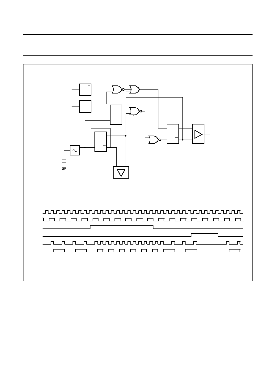
Clock circuitry (see Fig.5)
The clock signal (CLK) can be applied to the card in two
different methods:
1. Generation by a crystal oscillator: the crystal, or the
ceramic resonator (4 to 16 MHz) is connected to the
XTAL pin.
2. Use of a signal frequency (up to 20 MHz), already
present in the system and connected to the XTAL pin
via a 10 nF capacitor (see Fig.14). In both cases the
frequency is first divided-by-two.
If CMD7 (respectively CMD3.5) is LOW, the clock signal
(its frequency again divided by two) is enabled and
buffered before being fed to the CLK pin.
CMD3.5 and internal ENRST are sampled in order to give
the first clock pulse the correct width, and to avoid false
pulses during frequency change.
The CLKOUT2 pins may be used to clock a
microcontroller or an other TDA8001. The signal
1
/
2
f
xtal
is
available when the circuit is powered up.
State diagram
Once activated, the circuit has six possible modes of
operation:
∑
Idle
∑
Activation
∑
Read
∑
Write
∑
Deactivation
∑
Fault.
Figure 6 shows the way these modes are accessible.
I
DLE MODE
After reset, the circuit enters the IDLE state. A minimum
number of circuits are active while waiting for the
microcontroller to start a session.
∑
All card contacts are inactive
∑
I/O(
µ
C) is high impedance
∑
Voltage generators are stopped
∑
Oscillator or XTAL input is running, delivering CLKOUT2
∑
Voltage supervisors are active.
The DETECT line is HIGH if a card is present (PRES and
PRES active) and LOW if a card is not present. The OFF
line is HIGH if no hardware problem is detected.
A
CTIVATION SEQUENCE
From the IDLE mode, the circuit enters the ACTIVATION
mode when the microcontroller sets the CMDVCC line
(active LOW). The I/O(
µ
C) signal must not be LOW.
The internal circuitry is activated, the internal clock starts
and the sequence according to ISO7816 is performed:
∑
V
CC
rises from 0 to 5 V
∑
V
PP
rises from 0 to 5 V and I/O is enabled
∑
CLK and RST are enabled.
The time interval between steps 1 and 2 is 16
µ
s, and
64
µ
s between steps 2 and 3 (see Fig.7).
1996 Dec 12
8
Philips Semiconductors
Product specification
Smart card interface
TDA8001
R
EAD MODE
When the activation sequence is completed and, after the
card has replied its Answer-to-Reset, the TDA8001 will be
in the READ mode. Data is exchanged between the card
and the microcontroller via the I/O line.
W
RITE MODE
Cards with EPROM memory need a programming voltage
(V
PP
). When it is required to write to the internal memory
of the card, the microcontroller sets one of the VPP12.5,
VPP15 and VPP21 lines LOW, according to the
programming value given in the Answer-to-Reset.
V
PP
rises from 5 V to the selected value with a typical slew
rate of 0.38 V/
µ
s. In order to respect the ISO 7816 slopes,
the circuit generates V
PP
by charging and discharging an
internal capacitor. The voltage on this capacitor is then
amplified by a power stage gain of 5, powered via an
external supply pin V
H
(30 V max).
D
EACTIVATION SEQUENCE
(see Fig.8)
When the session is completed, the microcontroller sets
the CMDVCC line to its HIGH state. The circuit then
executes an automatic deactivation sequence by counting
the sequencer back:
∑
RST falls to LOW and CLK is stopped
∑
I/O(
µ
C) becomes high impedance and V
PP
falls to 0 V
∑
V
CC
falls to 0 V.
The circuit returns to the IDLE mode on the next rising
edge of the clock.
P
ROTECTIONS
Main fault conditions are monitored by the circuit:
∑
Short-circuit or overcurrent on V
CC
∑
Short-circuit or overcurrent on V
PP
∑
Card extraction during transaction
∑
Overheating problem
∑
V
SUP
drop-out
∑
V
DD
drop-out.
When one of these fault conditions is detected, the circuit
pulls the interrupt line OFF to its active LOW state and
returns to the FAULT mode. The current on I/O is internally
limited to 5 mA.
F
AULT MODE
(see Fig.9)
When a fault condition is written to the microcontroller via
the OFF line, the circuit initiates a deactivation sequence.
After the deactivation sequence has been completed, the
OFF line is reset to its HIGH state after the microcontroller
has reset the CMDVCC line HIGH.
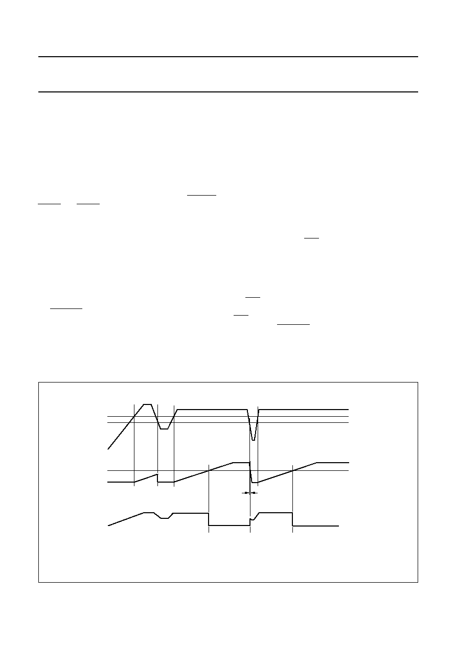
Fig.4 Alarm and delay as a function of V
SUP
(C
DEL
fixes the pulse width).
handbook, full pagewidth
MGG818
VSUP
Vth2
+
Vhys2
Vth2
Vth3
td
VDELAY
ALARM
1996 Dec 12
9
Philips Semiconductors
Product specification
Smart card interface
TDA8001
handbook, full pagewidth
MGG827
QB
QC
QD
ENCLK
QF
CLK
D
CK
CMD7 or CDMS = Z Z 1 1 0 0
CMD3.5 or CDMTC = 1 0 1 0 1 0
CLK = 2 4 0 4 2 4
Q
Q
CLK
D
CK
Q
Q
D
QI
QH
QD
QG
QA
QAA
QF
QB
QBA
QCA
QC
QE
ENCLK
1/2 CLKOUT
XTAL
CK
Q
Q
S
CDMTC
S
S
CDMS
S
Fig.5 Clock circuitry.

1996 Dec 12
10
Philips Semiconductors
Product specification
Smart card interface
TDA8001
Fig.6 State diagram.
handbook, full pagewidth
MGG820
FAULT
READ
WRITE
PDOWN
IDLE
ACTIVATION
DEACTIVATION
Fig.7 Activation sequence.
handbook, full pagewidth
MGG828
t2
tact
OFF
0
1
3
2
PRES
DETECT
CMDVCC
VEILLE
(INTERNAL)
INTERNAL
CLOCK
VCC
I/O
VPP
CMD3.5
CLK
ENRST
(INTERNAL)
RSTIN
RST
1996 Dec 12
11
Philips Semiconductors
Product specification
Smart card interface
TDA8001
Fig.8 Deactivation sequence.
handbook, full pagewidth
MGG829
tde
CMDVCC
3
0
1
2
VEILLE
(INTERNAL)
VCC
I/O
VPP
CMD3.5
CLK
ENRST
(INTERNAL)
RSTIN
RST
INTERNAL
CLOCK
Fig.9 Deactivation after a card extraction during write mode.
handbook, full pagewidth
MGG830
tde
PRES
3
0
1
2
DETECT
VCC
VPP
I/O
VEILLE
(INTERNAL)
ENRST
(INTERNAL)
CLK
RSTIN
RST
CMD3.5
CMDVCC
INTERNAL
CLOCK

1996 Dec 12
12
Philips Semiconductors
Product specification
Smart card interface
TDA8001
LIMITING VALUES
In accordance with the Absolute Maximum Rating System (IEC 134).
Note
1. P
tot
= V
DD
◊
(I
DD(unloaded)
+
I
signals
) + I
CC
◊
(V
DD
-
V
CC
) + max.{(V
H
-
V
PP
)
◊
I
PP(read)
+ (V
H
-
V
PP
)
◊
I
PP(write)
}
+ V
H
◊
I
H(unloaded)
+ V
SUP
◊
I
SUP
+ (V
DD
-
CVNC)
◊
I
CVNC
, where `signals' means all signal pins, except supply pins.
SYMBOL
PARAMETER
CONDITIONS
MIN.
MAX.
UNIT
V
DD
supply voltage
-
0.3
18
V
V
x1
voltage on pins VPP21, VPP15, VPP12.5, PRES,
PRES, CMDVCC, OFF, ALARM, DETECT and RSTIN
0
V
DD
V
V
H
voltage on pin V
H
0
30
V
V
PP
voltage on pin V
PP
0
V
H
V
V
SUP
voltage on pin V
SUP
0
12
V
V
x2
voltage on pins ALARM and DELAY
0
V
SUP
V
V
x3
voltage on pins XTAL, I/O(
µ
C), CLKOUT2, CMD7,
CMD3.5 and CVNC
0
6.0
V
V
x4
voltage on pins I/O, RST, CLK and V
CC
duration
<
1 ms
0
7.0
V
P
tot
continuous total power dissipation
TDA8001;
T
amb
= +70
∞
C; note 1;
see Fig.10
-
2
W
TDA8001T;
T
amb
= +70
∞
C; note 1;
see Fig.11
-
0.92
W
T
stg
storage temperature
-
55
+150
∞
C
V
es
electrostatic voltage on pins I/O, V
CC
, V
PP
, RST, CLK,
PRES and PRES
-
6
+6
kV
electrostatic voltage on other pins
-
2
+2
kV
1996 Dec 12
13
Philips Semiconductors
Product specification
Smart card interface
TDA8001
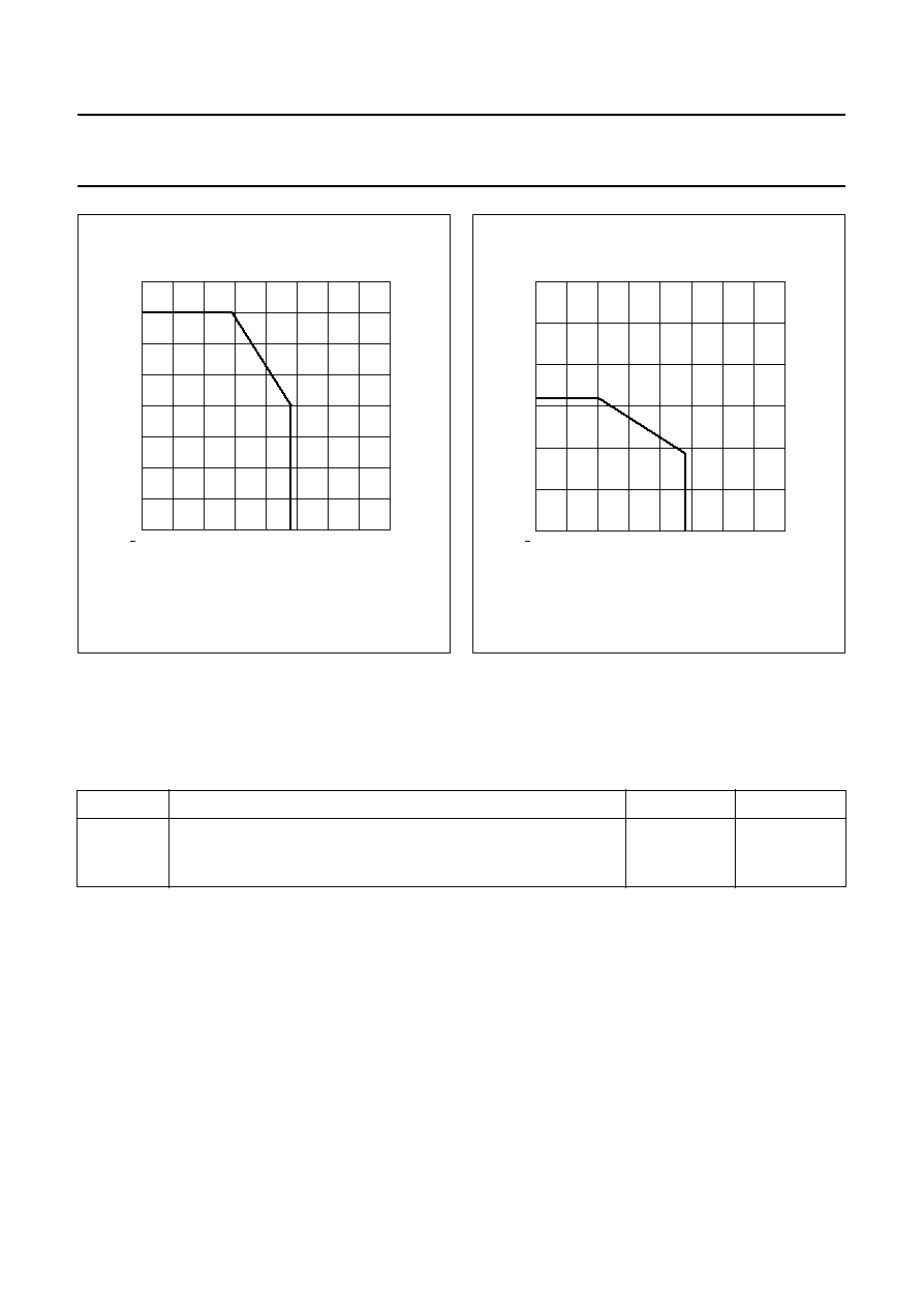
Fig.10 Power derating curve (DIP28).
handbook, halfpage
4
3
1
0
2
MBE256
50
0
50
100
150
Ptot
(W)
T ( C)
amb
o
Fig.11 Power derating curve (SO28).
handbook, halfpage
50
3
2
1
0
0
MBE255
50
100
150
Ptot
(W)
T ( C)
amb
o
HANDLING
Every pin withstands the ESD test according to MIL-STD-883C class 3 for card contacts, class 2 for the remaining.
Method 3015 (HBM 1500
, 100 pF) 3 pulses positive and 3 pulse negative on each pin referenced to ground.
THERMAL CHARACTERISTICS
SYMBOL
PARAMETER
VALUE
UNIT
R
th j-a
thermal resistance from junction to ambient in free air
SOT117-1
30
K/W
SOT136-1
70
K/W

1996 Dec 12
14
Philips Semiconductors
Product specification
Smart card interface
TDA8001
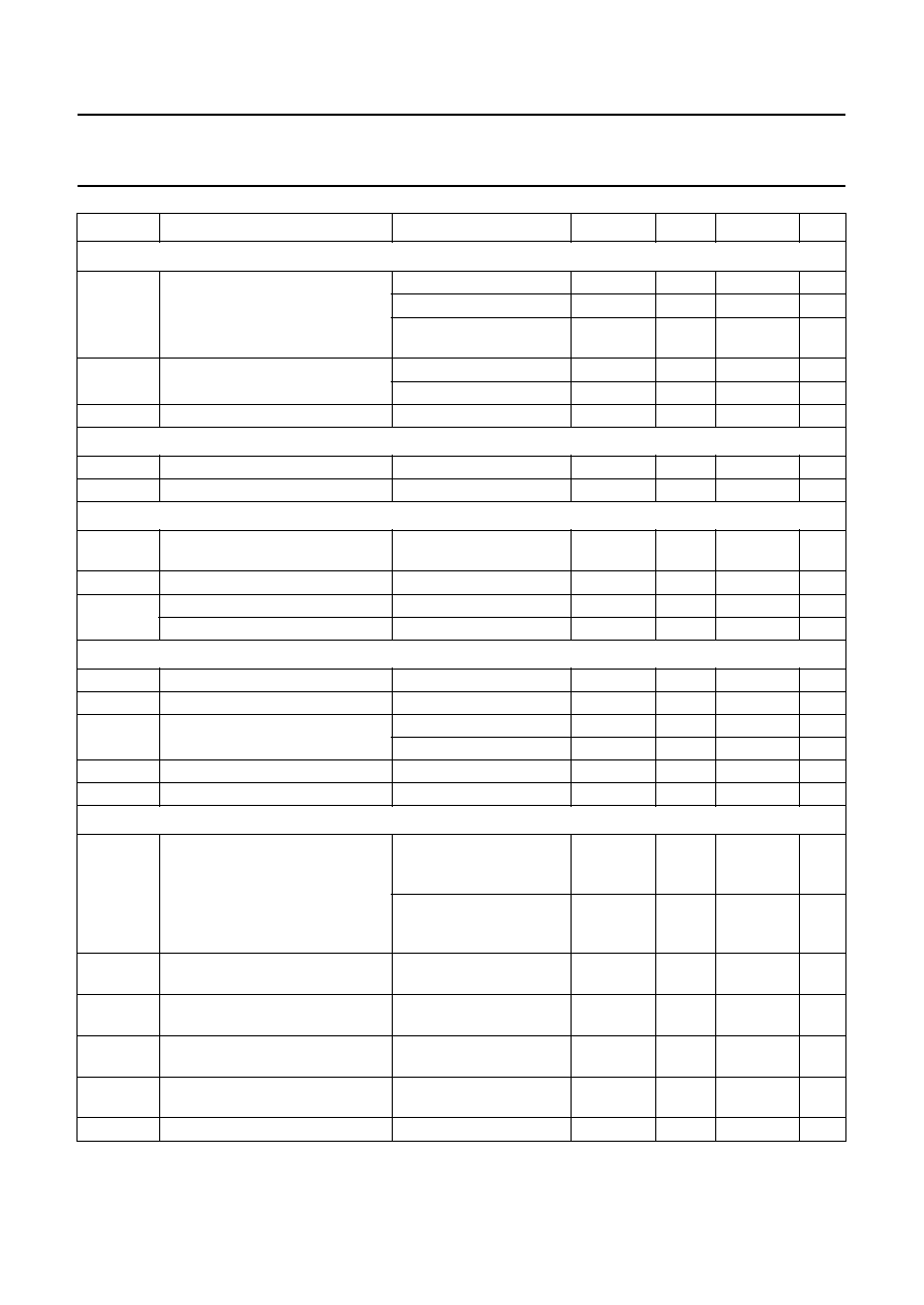
CHARACTERISTICS
V
DD
= 12 V; V
H
= 25 V; V
SUP
= 5 V; T
amb
= 25
∞
C; unless otherwise specified.
SYMBOL
PARAMETER
CONDITIONS
MIN.
TYP.
MAX.
UNIT
Supply
V
DD
supply voltage
6.7
-
18
V
I
DD
supply current
idle mode; V
DD
=
8 V
20
30
38
mA
idle mode; V
DD
=
18 V
22
34
42
mA
active mode; unloaded
35
45
55
mA
V
th1
threshold voltage for power-on
reset
-
3.0
4.0
V
V
th4
threshold voltage on V
DD
(falling)
6.0
-
6.5
V
V
hys4
hysteresis on V
th4
50
-
200
mV
Voltage supervisor
V
SUP
voltage supply for the supervisor
-
5.0
-
V
I
SUP
input current at V
SUP
-
1.8
2.4
mA
V
th2
threshold voltage on V
SUP
(falling)
4.5
-
4.72
V
V
hys2
hysteresis on V
th2
10
-
80
mV
V
th3
threshold voltage on DELAY
2.35
-
2.65
V
I
DEL
output current at DELAY
pin grounded (charge)
-
5
-
-
2
µ
A
V
DEL
=
4 V (discharge)
6
-
-
mA
V
DEL
voltage on pin DELAY
-
-
3.5
V
ALARM, ALARM (open-collector outputs)
I
OH
HIGH level output current on
pin ALARM
V
OH
=
5 V
-
-
25
µ
A
V
OL
LOW level output voltage on
pin ALARM
I
OL
=
2 mA
-
-
0.4
V
I
OL
LOW level output current on
pin ALARM
V
OL
=
0 V
-
-
-
25
µ
A
V
OH
HIGH level output voltage on
pin ALARM
I
OH
= -
2 mA
V
SUP
-
1
-
-
V
t
d
delay between V
SUP
and ALARM
C
DEL
=
47 nF; see Fig.4
-
-
10
µ
s
t
pulse
ALARM pulse width
C
DEL
=
47 nF
15
-
50
ms
Interrupt lines OFF and DETECT (open-collector)
I
OH
HIGH level output current
V
OH
=
5 V
-
-
25
µ
A
V
OL
LOW level output voltage
I
OL
=
1 mA
-
-
0.4
V
Logic inputs (CMDVCC, VPP21, VPP15, VPP12.5, CMD7, CMD3.5, PRES, PRES and RSTIN); note 1
V
IL
LOW level input voltage
-
-
0.8
V
V
IH
HIGH level input voltage
1.5
-
-
V
I
IL
LOW level input current
V
IL
=
0 V
-
-
-
10
µ
A
1996 Dec 12
15
Philips Semiconductors
Product specification
Smart card interface
TDA8001
I
IH
HIGH level input current
V
IH
=
5 V
-
-
10
µ
A
Reset output to the card (RST)
V
IDLE
output voltage in IDLE
-
-
0.4
V
V
OL
LOW level output voltage
I
OL
=
200
µ
A
-
-
0.45
V
V
OH
HIGH level output voltage
I
OH
= -
200
µ
A
4.3
-
V
CC
V
I
OH
= -
10
µ
A
V
CC
-
0.7
-
V
CC
V
t
RST
delay between RSTIN and RST
RST enabled; see Fig.7
-
-
2
µ
s
Clock output to the card (CLK)
V
IDLE
output voltage in IDLE
-
-
0.4
V
V
OL
LOW level output voltage
I
OL
=
200
µ
A
-
-
0.4
V
V
OH
HIGH level output voltage
I
OH
= -
200
µ
A
2.4
-
V
CC
V
I
OH
= -
20
µ
A
0.7V
CC
-
V
CC
V
I
OH
= -
10
µ
A
V
CC
-
0.7
-
V
CC
V
t
r
rise time
C
L
=
30 pF; note 2
-
-
14
ns
t
f
fall time
C
L
=
30 pF; note 2
-
-
14
ns
duty factor
C
L
=
30 pF; note 2
45
-
55
%
Card programming voltage (V
PP
)
V
PP
output voltage
idle mode
-
-
0.4
V
read mode
V
CC
-
4%
-
V
CC
+
4%
V
write mode; I
PP
< 50 mA
P
-
2.5%
(3)
-
P
+
2.5%
(3)
V
I
PP
/
t < 40 mA/100 ns;
note 4
P
-
2.5%
(3)
-
P
+
2.5%
(3)
V
I
PP
output current
active; from 0 to P
(3)
-
-
-
50
mA
V
PP
shorted to GND
-
-
-
100
mA
SR
slew rate
up or down
0.3
0.4
0.5
V/
µ
s
High voltage input (V
H
)
V
H
input voltage
-
-
30
V
I
H
input current at V
H
idle mode; active mode;
unloaded
4
-
6
mA
P = 5 V
5
-
9
mA
P = 12.5 V
6.5
-
10.5
mA
P = 15 V
7
-
11
mA
P = 21 V
8
-
12
mA
V
H
-
V
PP
voltage drop
-
-
2.2
V
SYMBOL
PARAMETER
CONDITIONS
MIN.
TYP.
MAX.
UNIT
1996 Dec 12
16
Philips Semiconductors
Product specification
Smart card interface
TDA8001
Card supply voltage (V
CC
)
V
CC
output voltage
idle mode; active mode
-
-
0.4
V
I
CC
< 100 mA
4.75
-
5.25
V
I
PP
/
t < 100 mA/100 ns
;
note 4
4.75
-
5.25
V
I
CC
output current
V
CC
from 0 to 5 V
-
-
-
100
mA
V
CC
shorted to GND
-
-
-
200
mA
SR
slew rate
up or down
0.3
0.4
0.5
V/
µ
s
5 V reference output voltage (CVNC)
V
CVNC
output voltage at pin CVNC
4.5
5.0
5.5
V
I
CVNC
output current at pin CVNC
-
-
-
50
mA
Crystal connection (XTAL)
R
xtal(neg)
negative resistance at pin XTAL
2 MHz < f
i
< 16 MHz;
note 5
-
-
300
V
xtal
DC voltage at pin XTAL
3.0
-
4.0
V
f
xtal
resonant frequency
4
-
16
MHz
external frequency
0
-
20
MHz
Clock output (CLKOUT2)
f
CLKOUT2
frequency on CLKOUT2
1
-
8
MHz
V
OL
LOW level output voltage
I
OL
=
2 mA
-
-
0.4
V
V
OH
HIGH level output voltage
I
OH
= -
200
µ
A
3.0
-
-
V
I
OH
= -
10
µ
A
4.0
-
-
V
t
r
, t
f
rise and fall times
C
L
=
15 pF; note 2
-
-
25
ns
duty factor
C
L
=
15 pF; note 2
40
-
60
%
Data line [I/O, I/O(
µ
C)]
V
OH
HIGH level output voltage on
pin I/O
4.5 V < V
SUP
< 5.5 V;
4.5 V < V
I/O(
µ
C)
< 5.5 V;
I
OH
= -
20
µ
A
4.0
-
V
CC
+ 0.1
V
4.5 V < V
SUP
< 5.5 V;
4.5 V < V
I/O(
µ
C)
< 5.5 V;
I
OH
=
-
200
µ
A
2.4
-
-
V
V
OL
LOW level output voltage on
pin I/O
I
I/O
= 1 mA;
I/O(
µ
C) grounded
-
-
100
mV
I
IL
LOW level input current on
pin I/O(
µ
C)
I/O(
µ
C) grounded
-
-
-
500
µ
A
V
OH
HIGH level output voltage on
pin I/O(
µ
C)
4.5 V < V
I/O
< 5.5 V
4.0
-
V
SUP
+ 0.2
V
V
OL
LOW level output voltage on
pin I/O(
µ
C)
I
I/O(
µ
C)
= 1 mA;
I/O grounded
-
-
70
mV
I
IL
LOW level input current on pin I/O I/O grounded
-
-
-
500
µ
A
SYMBOL
PARAMETER
CONDITIONS
MIN.
TYP.
MAX.
UNIT

1996 Dec 12
17
Philips Semiconductors
Product specification
Smart card interface
TDA8001
Notes
1. Pins CMDVCC, VPP21, VPP15, VPP12.5, CMD7, CMD3.5 and PRES are active LOW; pins RSTIN and PRES are
active HIGH.
2. The transition time and duty cycle definitions are shown in Fig.12;
.
3. P is the card programming voltage set by pin VPP12.5, VPP15 or VPP21.
4. The tests for dynamic response of both V
PP
and V
CC
are performed at 1 Hz, 10 kHz, 100 kHz and 1 MHz, with a
capacitive load of 100 nF.
5. This condition ensures proper starting of the oscillator with crystals having a series resistance up to 100
.
V
IDLE
voltage on pin I/O outside a
session
-
-
0.4
V
Z
IDLE
impedance on pin I/O(
µ
C)
outside a session
10
-
-
M
R
pu
internal pull-up resistance
between pin I/O and V
CC
8
10
12
k
t
r
, t
f
rise and fall times
C
i
= C
o
=
30 pF
-
-
0.5
µ
s
Protections
T
sd
shut-down local temperature
-
135
-
∞
C
I
CC(sd)
shut-down current at V
CC
-
-
150
-
mA
I
PP(sd)
shut-down current at V
PP
-
-
75
-
mA
I
I/O(lim)
current limitation on pin I/O
from I/O to I/O(
µ
C)
3
-
5
mA
Timing
t
act
activation sequence duration
see Fig.7
-
110
-
µ
s
t
de
deactivation sequence duration
see Fig.8
-
100
-
µ
s
t
3
start of the window for sending
CLK to the card
-
-
70
µ
s
t
5
end of the window for sending
CLK to the card
80
-
-
µ
s
t
st
maximum pulse width on
CMDVCC before V
CC
starts rising
-
-
30
µ
s
SYMBOL
PARAMETER
CONDITIONS
MIN.
TYP.
MAX.
UNIT
t
1
t
1
t
2
+
---------------
=
Fig.12 Definition of transition times.
handbook, full pagewidth
MBH856
10%
90%
10%
VOH
VOL
1.5 V
90%
tf
tr
t2
t1
1996 Dec 12
18
Philips Semiconductors
Product specification
Smart card interface
TDA8001
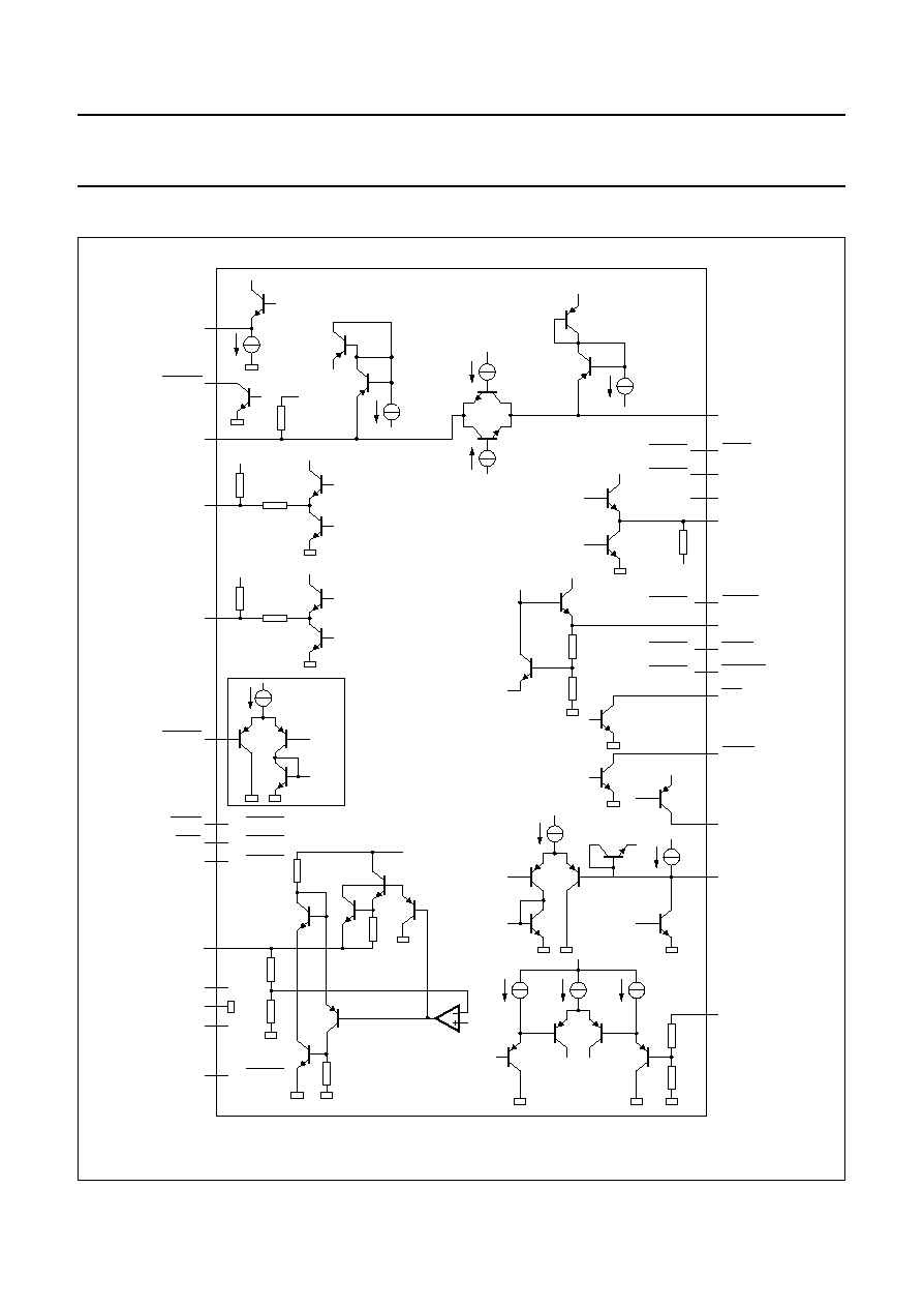
INTERNAL PIN CONFIGURATION
Fig.13 Internal pin configuration.
handbook, full pagewidth
MBE257
100
µ
A
20
µ
A
20
µ
A
5310
4690
VSUP
1.25 V
100
µ
A
2.5 V
VSUP
2.5
µ
A
DELAY
ALARM
VSUP
ALARM
OFF
CMDVCC
VPP21
650
1350
DD
V
CMD3.5
CVNC
CLKOUT2
RSTIN
CMD7
GND2
100
µ
A
100
µ
A
I/O(
µ
C)
VSUP
100
µ
A
VCC
100
µ
A
100
µ
A
VCC
VCC
5 k
100
VCC
RST
XTAL
I/O
DETECT
VCC
10 k
50
VCC
CLK
20
µ
A
1.25 V
VPP12.5
TDA8001
2.5 V
VH
VPP15
PRES
PRES
VPP
V H
GND1
VDD
VCC
5 V
as VPP12.5
as VPP12.5
as VPP12.5
as VPP12.5
as VPP12.5
as VPP12.5
as VPP12.5
as VPP12.5
as VPP12.5
1996 Dec 12
19
Philips Semiconductors
Product specification
Smart card interface
TDA8001
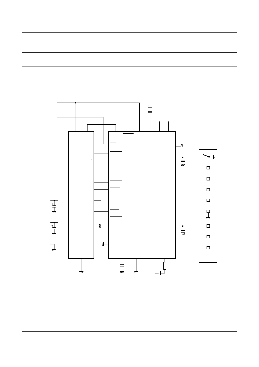
APPLICATION INFORMATION
Fig.14 Application in a pay TV decoder.
(1) The capacitor should be placed as close as possible to the IC.
(2) If pin V
H
is not connected to 25 V, it should be connected to V
DD
.
handbook, full pagewidth
MGG831
10
µ
F
10
µ
F
C1
C2
C3
DETECT
RSTIN
I/O(
µ
C)
CMD7
CLKOUT2
GND2
OFF
VDD
VDD
VSUP
VH
RST
CVNC
12 V 25 V
ALARM
TDA8001
ALARM
DELAY
GND
GND1
XTAL
47 nF
14 MHz
C5
C6
C8
CARD
SOCKET
80C52
MICRO-
CONTROLLER
to 8805
micro-
controller
PORT
1
PORT
2
INT0
100 nF
(1)
XTAL1
I/O
CLK
RST
VCC
PRES
PRES
VPP
XTAL2
25 V
GND
12 V
+
5 V
C7
C4
100 nF
100 nF
47 nF
CMD3.5
CMDVCC
VPP15
VPP21
VPP12.5
1 k
(2)
1996 Dec 12
20
Philips Semiconductors
Product specification
Smart card interface
TDA8001
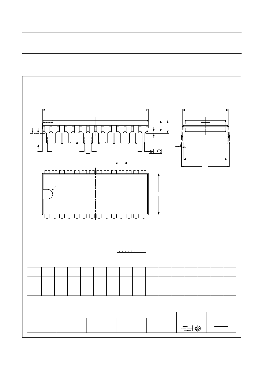
PACKAGE OUTLINES
UNIT
A
max.
1
2
b
1
(1)
(1)
(1)
c
D
E
w
e
M
H
L
REFERENCES
OUTLINE
VERSION
EUROPEAN
PROJECTION
ISSUE DATE
IEC
JEDEC
EIAJ
mm
inches
DIMENSIONS (inch dimensions are derived from the original mm dimensions)
SOT117-1
92-11-17
95-01-14
A
min.
A
max.
b
Z
max.
M
E
e
1
1.7
1.3
0.53
0.38
0.32
0.23
36.0
35.0
14.1
13.7
3.9
3.4
0.25
2.54
15.24
15.80
15.24
17.15
15.90
1.7
5.1
0.51
4.0
0.066
0.051
0.020
0.014
0.013
0.009
1.41
1.34
0.56
0.54
0.15
0.13
0.01
0.10
0.60
0.62
0.60
0.68
0.63
0.067
0.20
0.020
0.16
051G05
MO-015AH
M
H
c
(e )
1
M
E
A
L
seating plane
A
1
w
M
b
1
e
D
A
2
Z
28
1
15
14
b
E
pin 1 index
0
5
10 mm
scale
Note
1. Plastic or metal protrusions of 0.25 mm maximum per side are not included.
handbook, full pagewidth
DIP28: plastic dual in-line package; 28 leads (600 mil)
SOT117-1

1996 Dec 12
21
Philips Semiconductors
Product specification
Smart card interface
TDA8001
UNIT
A
max.
A
1
A
2
A
3
b
p
c
D
(1)
E
(1)
(1)
e
H
E
L
L
p
Q
Z
y
w
v
REFERENCES
OUTLINE
VERSION
EUROPEAN
PROJECTION
ISSUE DATE
IEC
JEDEC
EIAJ
mm
inches
2.65
0.30
0.10
2.45
2.25
0.49
0.36
0.32
0.23
18.1
17.7
7.6
7.4
1.27
10.65
10.00
1.1
1.0
0.9
0.4
8
0
o
o
0.25
0.1
DIMENSIONS (inch dimensions are derived from the original mm dimensions)
Note
1. Plastic or metal protrusions of 0.15 mm maximum per side are not included.
1.1
0.4
SOT136-1
91-08-13
95-01-24
X
14
28
w
M
A
A
1
A
2
b
p
D
H
E
L
p
Q
detail X
E
Z
c
L
v
M
A
e
15
1
(A )
3
A
y
0.25
075E06
MS-013AE
pin 1 index
0.10
0.012
0.004
0.096
0.089
0.019
0.014
0.013
0.009
0.71
0.69
0.30
0.29
0.050
1.4
0.055
0.42
0.39
0.043
0.039
0.035
0.016
0.01
0.25
0.01
0.004
0.043
0.016
0.01
0
5
10 mm
scale
SO28: plastic small outline package; 28 leads; body width 7.5 mm
SOT136-1

1996 Dec 12
22
Philips Semiconductors
Product specification
Smart card interface
TDA8001
SOLDERING
Introduction
There is no soldering method that is ideal for all IC
packages. Wave soldering is often preferred when
through-hole and surface mounted components are mixed
on one printed-circuit board. However, wave soldering is
not always suitable for surface mounted ICs, or for
printed-circuits with high population densities. In these
situations reflow soldering is often used.
This text gives a very brief insight to a complex technology.
A more in-depth account of soldering ICs can be found in
our
"IC Package Databook" (order code 9398 652 90011).
DIP
S
OLDERING BY DIPPING OR BY WAVE
The maximum permissible temperature of the solder is
260
∞
C; solder at this temperature must not be in contact
with the joint for more than 5 seconds. The total contact
time of successive solder waves must not exceed
5 seconds.
The device may be mounted up to the seating plane, but
the temperature of the plastic body must not exceed the
specified maximum storage temperature (T
stg max
). If the
printed-circuit board has been pre-heated, forced cooling
may be necessary immediately after soldering to keep the
temperature within the permissible limit.
R
EPAIRING SOLDERED JOINTS
Apply a low voltage soldering iron (less than 24 V) to the
lead(s) of the package, below the seating plane or not
more than 2 mm above it. If the temperature of the
soldering iron bit is less than 300
∞
C it may remain in
contact for up to 10 seconds. If the bit temperature is
between 300 and 400
∞
C, contact may be up to 5 seconds.
SO
R
EFLOW SOLDERING
Reflow soldering techniques are suitable for all SO
packages.
Reflow soldering requires solder paste (a suspension of
fine solder particles, flux and binding agent) to be applied
to the printed-circuit board by screen printing, stencilling or
pressure-syringe dispensing before package placement.
Several techniques exist for reflowing; for example,
thermal conduction by heated belt. Dwell times vary
between 50 and 300 seconds depending on heating
method. Typical reflow temperatures range from
215 to 250
∞
C.
Preheating is necessary to dry the paste and evaporate
the binding agent. Preheating duration: 45 minutes at
45
∞
C.
W
AVE SOLDERING
Wave soldering techniques can be used for all SO
packages if the following conditions are observed:
∑
A double-wave (a turbulent wave with high upward
pressure followed by a smooth laminar wave) soldering
technique should be used.
∑
The longitudinal axis of the package footprint must be
parallel to the solder flow.
∑
The package footprint must incorporate solder thieves at
the downstream end.
During placement and before soldering, the package must
be fixed with a droplet of adhesive. The adhesive can be
applied by screen printing, pin transfer or syringe
dispensing. The package can be soldered after the
adhesive is cured.
Maximum permissible solder temperature is 260
∞
C, and
maximum duration of package immersion in solder is
10 seconds, if cooled to less than 150
∞
C within
6 seconds. Typical dwell time is 4 seconds at 250
∞
C.
A mildly-activated flux will eliminate the need for removal
of corrosive residues in most applications.
R
EPAIRING SOLDERED JOINTS
Fix the component by first soldering two diagonally-
opposite end leads. Use only a low voltage soldering iron
(less than 24 V) applied to the flat part of the lead. Contact
time must be limited to 10 seconds at up to 300
∞
C.
When using a dedicated tool, all other leads can be
soldered in one operation within 2 to 5 seconds between
270 and 320
∞
C.

1996 Dec 12
23
Philips Semiconductors
Product specification
Smart card interface
TDA8001
DEFINITIONS
LIFE SUPPORT APPLICATIONS
These products are not designed for use in life support appliances, devices, or systems where malfunction of these
products can reasonably be expected to result in personal injury. Philips customers using or selling these products for
use in such applications do so at their own risk and agree to fully indemnify Philips for any damages resulting from such
improper use or sale.
Data sheet status
Objective specification
This data sheet contains target or goal specifications for product development.
Preliminary specification
This data sheet contains preliminary data; supplementary data may be published later.
Product specification
This data sheet contains final product specifications.
Limiting values
Limiting values given are in accordance with the Absolute Maximum Rating System (IEC 134). Stress above one or
more of the limiting values may cause permanent damage to the device. These are stress ratings only and operation
of the device at these or at any other conditions above those given in the Characteristics sections of the specification
is not implied. Exposure to limiting values for extended periods may affect device reliability.
Application information
Where application information is given, it is advisory and does not form part of the specification.

Internet: http://www.semiconductors.philips.com
Philips Semiconductors ≠ a worldwide company
© Philips Electronics N.V. 1996
SCA52
All rights are reserved. Reproduction in whole or in part is prohibited without the prior written consent of the copyright owner.
The information presented in this document does not form part of any quotation or contract, is believed to be accurate and reliable and may be changed
without notice. No liability will be accepted by the publisher for any consequence of its use. Publication thereof does not convey nor imply any license
under patent- or other industrial or intellectual property rights.
Netherlands: Postbus 90050, 5600 PB EINDHOVEN, Bldg. VB,
Tel. +31 40 27 82785, Fax. +31 40 27 88399
New Zealand: 2 Wagener Place, C.P.O. Box 1041, AUCKLAND,
Tel. +64 9 849 4160, Fax. +64 9 849 7811
Norway: Box 1, Manglerud 0612, OSLO,
Tel. +47 22 74 8000, Fax. +47 22 74 8341
Philippines: Philips Semiconductors Philippines Inc.,
106 Valero St. Salcedo Village, P.O. Box 2108 MCC, MAKATI,
Metro MANILA, Tel. +63 2 816 6380, Fax. +63 2 817 3474
Poland: Ul. Lukiska 10, PL 04-123 WARSZAWA,
Tel. +48 22 612 2831, Fax. +48 22 612 2327
Portugal: see Spain
Romania: see Italy
Russia: Philips Russia, Ul. Usatcheva 35A, 119048 MOSCOW,
Tel. +7 095 247 9145, Fax. +7 095 247 9144
Singapore: Lorong 1, Toa Payoh, SINGAPORE 1231,
Tel. +65 350 2538, Fax. +65 251 6500
Slovakia: see Austria
Slovenia: see Italy
South Africa: S.A. PHILIPS Pty Ltd., 195-215 Main Road Martindale,
2092 JOHANNESBURG, P.O. Box 7430 Johannesburg 2000,
Tel. +27 11 470 5911, Fax. +27 11 470 5494
South America: Rua do Rocio 220, 5th floor, Suite 51,
04552-903 S„o Paulo, S√O PAULO - SP, Brazil,
Tel. +55 11 821 2333, Fax. +55 11 829 1849
Spain: Balmes 22, 08007 BARCELONA,
Tel. +34 3 301 6312, Fax. +34 3 301 4107
Sweden: Kottbygatan 7, Akalla, S-16485 STOCKHOLM,
Tel. +46 8 632 2000, Fax. +46 8 632 2745
Switzerland: Allmendstrasse 140, CH-8027 ZÐRICH,
Tel. +41 1 488 2686, Fax. +41 1 481 7730
Taiwan: PHILIPS TAIWAN Ltd., 23-30F, 66,
Chung Hsiao West Road, Sec. 1, P.O. Box 22978,
TAIPEI 100, Tel. +886 2 382 4443, Fax. +886 2 382 4444
Thailand: PHILIPS ELECTRONICS (THAILAND) Ltd.,
209/2 Sanpavuth-Bangna Road Prakanong, BANGKOK 10260,
Tel. +66 2 745 4090, Fax. +66 2 398 0793
Turkey: Talatpasa Cad. No. 5, 80640 GÐLTEPE/ISTANBUL,
Tel. +90 212 279 2770, Fax. +90 212 282 6707
Ukraine: PHILIPS UKRAINE, 4 Patrice Lumumba str., Building B, Floor 7,
252042 KIEV, Tel. +380 44 264 2776, Fax. +380 44 268 0461
United Kingdom: Philips Semiconductors Ltd., 276 Bath Road, Hayes,
MIDDLESEX UB3 5BX, Tel. +44 181 730 5000, Fax. +44 181 754 8421
United States: 811 East Arques Avenue, SUNNYVALE, CA 94088-3409,
Tel. +1 800 234 7381
Uruguay: see South America
Vietnam: see Singapore
Yugoslavia: PHILIPS, Trg N. Pasica 5/v, 11000 BEOGRAD,
Tel. +381 11 625 344, Fax.+381 11 635 777
For all other countries apply to: Philips Semiconductors, Marketing & Sales Communications,
Building BE-p, P.O. Box 218, 5600 MD EINDHOVEN, The Netherlands, Fax. +31 40 27 24825
Argentina: see South America
Australia: 34 Waterloo Road, NORTH RYDE, NSW 2113,
Tel. +61 2 9805 4455, Fax. +61 2 9805 4466
Austria: Computerstr. 6, A-1101 WIEN, P.O. Box 213,
Tel. +43 1 60 101, Fax. +43 1 60 101 1210
Belarus: Hotel Minsk Business Center, Bld. 3, r. 1211, Volodarski Str. 6,
220050 MINSK, Tel. +375 172 200 733, Fax. +375 172 200 773
Belgium: see The Netherlands
Brazil: see South America
Bulgaria: Philips Bulgaria Ltd., Energoproject, 15th floor,
51 James Bourchier Blvd., 1407 SOFIA,
Tel. +359 2 689 211, Fax. +359 2 689 102
Canada: PHILIPS SEMICONDUCTORS/COMPONENTS,
Tel. +1 800 234 7381
China/Hong Kong: 501 Hong Kong Industrial Technology Centre,
72 Tat Chee Avenue, Kowloon Tong, HONG KONG,
Tel. +852 2319 7888, Fax. +852 2319 7700
Colombia: see South America
Czech Republic: see Austria
Denmark: Prags Boulevard 80, PB 1919, DK-2300 COPENHAGEN S,
Tel. +45 32 88 2636, Fax. +45 31 57 1949
Finland: Sinikalliontie 3, FIN-02630 ESPOO,
Tel. +358 9 615800, Fax. +358 9 61580/xxx
France: 4 Rue du Port-aux-Vins, BP317, 92156 SURESNES Cedex,
Tel. +33 1 40 99 6161, Fax. +33 1 40 99 6427
Germany: Hammerbrookstraþe 69, D-20097 HAMBURG,
Tel. +49 40 23 53 60, Fax. +49 40 23 536 300
Greece: No. 15, 25th March Street, GR 17778 TAVROS/ATHENS,
Tel. +30 1 4894 339/239, Fax. +30 1 4814 240
Hungary: see Austria
India: Philips INDIA Ltd, Shivsagar Estate, A Block, Dr. Annie Besant Rd.
Worli, MUMBAI 400 018, Tel. +91 22 4938 541, Fax. +91 22 4938 722
Indonesia: see Singapore
Ireland: Newstead, Clonskeagh, DUBLIN 14,
Tel. +353 1 7640 000, Fax. +353 1 7640 200
Israel: RAPAC Electronics, 7 Kehilat Saloniki St, TEL AVIV 61180,
Tel. +972 3 645 0444, Fax. +972 3 649 1007
Italy: PHILIPS SEMICONDUCTORS, Piazza IV Novembre 3,
20124 MILANO, Tel. +39 2 6752 2531, Fax. +39 2 6752 2557
Japan: Philips Bldg 13-37, Kohnan 2-chome, Minato-ku, TOKYO 108,
Tel. +81 3 3740 5130, Fax. +81 3 3740 5077
Korea: Philips House, 260-199 Itaewon-dong, Yongsan-ku, SEOUL,
Tel. +82 2 709 1412, Fax. +82 2 709 1415
Malaysia: No. 76 Jalan Universiti, 46200 PETALING JAYA, SELANGOR,
Tel. +60 3 750 5214, Fax. +60 3 757 4880
Mexico: 5900 Gateway East, Suite 200, EL PASO, TEXAS 79905,
Tel. +9-5 800 234 7381
Middle East: see Italy
Printed in The Netherlands
537021/1200/02/pp24
Date of release: 1996 Dec 12
Document order number:
9397 750 01384