 | –≠–ª–µ–∫—Ç—Ä–æ–Ω–Ω—ã–π –∫–æ–º–ø–æ–Ω–µ–Ω—Ç: TDA8004 | –°–∫–∞—á–∞—Ç—å:  PDF PDF  ZIP ZIP |
DATA SHEET
Product specification
Supersedes data of 2000 Feb 29
2004 May 10
INTEGRATED CIRCUITS
TDA8004AT
IC card interface

2004 May 10
2
Philips Semiconductors
Product specification
IC card interface
TDA8004AT
FEATURES
∑
3 or 5 V supply for the IC (GND and V
DD
)
∑
Step-up converter for V
CC
generation (separately
powered with a 5 V
±
10% supply, V
DDP
and PGND)
∑
3 specific protected half duplex bidirectional buffered I/O
lines (C4, C7 and C8)
∑
V
CC
regulation (5 or 3 V
±
5% on 2
◊
100 nF or
1
◊
100 nF and 1
◊
220 nF multilayer ceramic
capacitors with low ESR, I
CC
< 65 mA at
4.5 V < V
DDP
< 6.5 V, current spikes of 40 nAs up to
20 MHz, with controlled rise and fall times, filtered
overload detection approximately 90 mA)
∑
Thermal and short-circuit protections on all card
contacts
∑
Automatic activation and deactivation sequences
(initiated by software or by hardware in the event of a
short-circuit, card take-off, overheating or supply
drop-out)
∑
Enhanced ESD protection on card side (>6 kV)
∑
26 MHz integrated crystal oscillator
∑
Clock generation for the card up to 20 MHz (divided by
1, 2, 4 or 8 through CLKDIV1 and CLKDIV2 signals)
with synchronous frequency changes
∑
Non-inverted control of RST via pin RSTIN
∑
ISO 7816, GSM11.11 and EMV (payment systems)
compatibility
∑
Supply supervisor for spikes killing during power-on
and power-off
∑
One multiplexed status signal OFF.
APPLICATIONS
∑
IC card readers for banking
∑
Electronic payment
∑
Identification
∑
Pay TV.
GENERAL DESCRIPTION
The TDA8004AT is a complete low cost analog interface
for asynchronous 3 or 5 V smart cards. It can be placed
between the card and the microcontroller with very few
external components to perform all supply protection and
control functions.
ORDERING INFORMATION
TYPE
NUMBER
PACKAGE
NAME
DESCRIPTION
VERSION
TDA8004AT
SO28
plastic small outline package; 28 leads; body width 7.5 mm
SOT136-1

2004 May 10
3
Philips Semiconductors
Product specification
IC card interface
TDA8004AT
QUICK REFERENCE DATA
SYMBOL
PARAMETER
CONDITIONS
MIN.
TYP.
MAX.
UNIT
Supplies
V
DD
supply voltage
2.7
-
6.5
V
V
DDP
step-up supply voltage
4.5
5
6.5
V
I
DD
supply current
inactive mode; V
DD
= 3.3 V;
f
XTAL
= 10 MHz
-
-
1.2
mA
active mode; V
DD
= 3.3 V;
f
XTAL
= 10 MHz; no load
-
-
1.5
mA
I
DDP
supply current step-up converter
inactive mode; V
DDP
= 5 V;
f
XTAL
= 10 MHz
-
-
0.1
mA
active mode; V
DDP
= 5 V;
f
XTAL
= 10 MHz; no load
-
-
18
mA
Card supply
V
CC
output voltage including ripple
5 V card
DC
I
CC
< 65 mA
4.75
-
5.25
V
AC current spikes of 40 nAs
4.65
-
5.25
V
3 V card
DC
I
CC
< 65 mA
2.85
-
3.15
V
AC current spikes of 40 nAs
2.76
-
3.20
V
V
i(ripple)(p-p)
peak-to-peak ripple voltage on V
CC
from 20 kHz to 200 MHz
-
-
350
mV
I
CC
output current
V
CC
from 0 to 5 or to 3 V
-
-
65
mA
General
f
CLK
card clock frequency
0
-
20
MHz
t
de
deactivation cycle duration
60
80
100
µ
s
P
tot
continuous total power dissipation
T
amb
=
-
25 to +85
∞
C
-
-
0.56
W
T
amb
ambient temperature
-
25
-
+85
∞
C

2004 May 10
4
Philips Semiconductors
Product specification
IC card interface
TDA8004AT
BLOCK DIAGRAM
handbook, full pagewidth
FCE658
100 nF
100 nF
100 nF
100 nF
100
nF
100
nF
I/O
TRANSCEIVER
I/O
TRANSCEIVER
I/O
TRANSCEIVER
THERMAL
PROTECTION
VCC
GENERATOR
RST
BUFFER
CLOCK
BUFFER
SEQUENCER
CLOCK
CIRCUITRY
OSCILLATOR
HORSEQ
INTERNAL OSCILLATOR
2.5 MHz
STEP-UP CONVERTER
INTERNAL
REFERENCE
VOLTAGE SENSE
SUPPLY
EN2
PVCC
EN5
EN4
EN3
CLK
EN1
CLKUP
ALARM
Vref
21
VDD
6
VDDP
7
5
S1
S2
8 VUP
4 PGND
17
VCC
16
14
RST
CGND
PRES
10
9
PRES
15
CLK
13
12
11
AUX1
AUX2
I/O
22
18
n.c.
GND
26
28
27
I/OUC
AUX2UC
AUX1UC
25
24
2
1
3
19
20
23
XTAL2
XTAL1
CLKDIV2
CLKDIV1
5V/3V
CMDVCC
RSTIN
OFF
TDA8004AT
Fig.1 Block diagram.
All capacitors are mandatory.

2004 May 10
5
Philips Semiconductors
Product specification
IC card interface
TDA8004AT
PINNING
SYMBOL
PIN
I/O
DESCRIPTION
CLKDIV1
1
I
control with CLKDIV2 for choosing CLK frequency
CLKDIV2
2
I
control with CLKDIV1 for choosing CLK frequency
5V/3V
3
I
control signal for selecting V
CC
= 5 V (HIGH) or V
CC
= 3 V (LOW)
PGND
4
supply
power ground for step-up converter
S2
5
I/O
capacitance connection for step-up converter (a 100 nF capacitor with ESR < 100 m
must be connected between pins S1 and S2)
V
DDP
6
supply
power supply voltage for step-up converter
S1
7
I/O
capacitance connection for step-up converter (a 100 nF capacitor with ESR < 100 m
must be connected between pins S1 and S2)
VUP
8
O
output of step-up converter (a 100 nF capacitor with ESR < 100 m
must be connected
to PGND)
PRES
9
I
card presence contact input (active LOW); if PRES or PRES is true, then the card is
considered as present
PRES
10
I
card presence contact input (active HIGH); if PRES or PRES is true, then the card is
considered as present
I/O
11
I/O
data line to and from card (C7) (internal 10 k
pull-up resistor connected to V
CC
)
AUX2
12
I/O
auxiliary line to and from card (C8) (internal 10 k
pull-up resistor connected to V
CC
)
AUX1
13
I/O
auxiliary line to and from card (C4) (internal 10 k
pull-up resistor connected to V
CC
)
CGND
14
supply
ground for card signals
CLK
15
O
clock to card (C3)
RST
16
O
card reset (C2)
V
CC
17
O
supply for card (C1); decouple to CGND with 2
◊
100 nF or 1
◊
100nF and 1
◊
220 nF
capacitors with ESR < 100 m
(with 220 nF, the noise margin on V
CC
will be higher)
n.c.
18
-
not connected
CMDVCC
19
I
start activation sequence input from microcontroller (active LOW)
RSTIN
20
I
card reset input from microcontroller (active HIGH)
V
DD
21
supply
supply voltage
GND
22
supply
ground
OFF
23
O
NMOS interrupt to microcontroller (active LOW) with 20 k
internal pull-up resistor
connected to V
DD
(refer section "Fault detection")
XTAL1
24
I
crystal connection or input for external clock
XTAL2
25
O
crystal connection (leave open circuit if an external clock source is used)
I/OUC
26
I/O
microcontroller data I/O line (internal 10 k
pull-up resistor connected to V
DD
)
AUX1UC
27
I/O
auxiliary line to and from microcontroller (internal 10 k
pull-up resistor connected to
V
DD
)
AUX2UC
28
I/O
auxiliary line to and from microcontroller (internal 10 k
pull-up resistor connected to
V
DD
)
2004 May 10
6
Philips Semiconductors
Product specification
IC card interface
TDA8004AT
FUNCTIONAL DESCRIPTION
Throughout this document, it is assumed that the reader is
familiar with ISO7816 norm terminology.
Power supply
The supply pins for the IC are V
DD
and GND. V
DD
should
be in the range from 2.7 to 6.5 V. All interface signals with
the microcontroller are referenced to V
DD
; therefore be
sure the supply voltage of the microcontroller is also at
V
DD
. All card contacts remain inactive during powering up
or powering down. The sequencer is not activated until
V
DD
reaches V
th2
+ V
hys(th2)
(see Fig.3). When V
DD
falls
below V
th2
, an automatic deactivation of the contacts is
performed.
For generating a 5 V
±
5% V
CC
supply to the card, an
integrated voltage doubler is incorporated. This step-up
converter should be separately supplied by V
DDP
and
PGND (from 4.5 to 6.5 V). Due to large transient currents,
the 2
◊
100 nF capacitors of the step-up converter should
have an ESR of less than 100 m
, and be located as near
as possible to the IC.
The supply voltages V
DD
and V
DDP
may be applied to the
IC in any time sequence.
If a voltage between 7 and 9 V is available within the
application, this voltage may be tied to pin VUP, thus
blocking the step-up converter. In this case, V
DDP
must be
tied to V
DD
and the capacitor between pins S1 and S2 may
be omitted.
Voltage supervisor
This block surveys the V
DD
supply. A defined reset pulse
of approximately 10 ms (t
W
) is used internally for
maintaining the IC in the inactive mode during powering up
or powering down of V
DD
(see Fig.3)).
As long as V
DD
is less than V
th2
+ V
hys(th2)
, the IC will
remain inactive whatever the levels on the command lines.
This also lasts for the duration of t
W
after V
DD
has reached
a level higher than V
th2
+ V
hys(th2)
.
The system controller should not attempt to start an
activation sequence during this time.
When V
DD
falls below V
th2
, a deactivation sequence of the
contacts is performed.
CLKDIV1
CLKDIV2
5V/3V
PGND
S2
VDDP
S1
VUP
PRES
PRES
I/O
AUX2
AUX1
CGND
AUX2UC
AUX1UC
I/OUC
XTAL2
OFF
GND
XTAL1
VDD
RSTIN
CMDVCC
n.c.
VCC
RST
CLK
1
2
3
4
5
6
7
8
9
10
11
12
13
28
27
26
25
24
23
22
21
20
19
18
17
16
15
14
TDA8004AT
FCE659
Fig.2 Pin configuration.

2004 May 10
7
Philips Semiconductors
Product specification
IC card interface
TDA8004AT
FCE660
VDD
tW
tW
Vth2
+
Vhys(th2)
Vth2
ALARM
(internal signal)
Fig.3 Alarm as a function of V
DD
(t
W
= 10 ms).
Clock circuitry
The clock signal (CLK) to the card is either derived from a
clock signal input on pin XTAL1 or from a crystal up to
26 MHz connected between pins XTAL1 and XTAL2.
The frequency may be chosen at f
XTAL
,
1
/
2
f
XTAL
,
1
/
4
f
XTAL
or
1
/
8
f
XTAL
via pins CLKDIV1 and CLKDIV2.
The frequency change is synchronous, which means that
during transition, no pulse is shorter than 45% of the
smallest period and that the first and last clock pulse
around the change has the correct width.
In the case of f
XTAL
, the duty factors are dependent on the
signal at XTAL1.
In order to reach a 45% to 55% duty factor on pin CLK the
input signal on XTAL1 should have a duty factor of
48% to 52% and transition times of less than 5% of the
input signal period.
If a crystal is used with f
XTAL
, the duty factor on pin CLK
may be 45% to 55% depending on the layout and on the
crystal characteristics and frequency.
In the other cases, it is guaranteed between 45% and 55%
of the period.
The crystal oscillator runs as soon as the IC is
powered-up. If the crystal oscillator is used, or if the clock
pulse on XTAL1 is permanent, then the clock pulse will be
applied to the card according to the timing diagram of the
activation sequence (see Fig.5).
If the signal applied to XTAL1 is controlled by the
microcontroller, then the clock pulse will be applied to the
card by the microcontroller after completion of the
activation sequence.
Table 1
Clock circuitry definition
CLKDIV1
CLKDIV2
CLK
0
0
1
/
8
f
XTAL
0
1
1
/
4
f
XTAL
1
1
1
/
2
f
XTAL
1
0
f
XTAL
2004 May 10
8
Philips Semiconductors
Product specification
IC card interface
TDA8004AT
I/O circuitry
The three data lines I/O, AUX1 and AUX2 are identical.
The Idle state is realized by data lines I/O and I/OUC being
pulled HIGH via a 10 k
resistor (I/O to V
CC
and I/OUC to
V
DD
).
I/O is referenced to V
CC
, and I/OUC to V
DD
, thus allowing
operation with V
CC
V
DD
.
The first line on which a falling edge occurs becomes the
master. An anti-latch circuit disables the detection of falling
edges on the other line, which then becomes the slave.
After a time delay t
d(edge)
(approximately 200 ns), the
N transistor on the slave line is turned on, thus transmitting
the logic 0 present on the master line.
When the master line returns to logic 1, the P transistor on
the slave line is turned on during the time delay t
d(edge)
and
then both lines return to their Idle states.
This active pull-up feature ensures fast LOW-to-HIGH
transitions; it is able to deliver more than 1 mA up to an
output voltage of 0.9V
CC
on a 80 pF load. At the end of the
active pull-up pulse, the output voltage only depends on
the internal pull-up resistor, and on the load current (see
Fig.4).
The maximum frequency on these lines is 1 MHz.
Inactive state
After power-on reset, the circuit enters the inactive state.
A minimum number of circuits are active while waiting for
the microcontroller to start a session.
∑
All card contacts are inactive (approximately 200
to GND)
∑
I/OUC, AUX1UC and AUX2UC are high impedance
(10 k
pull-up resistor connected to V
DD
)
∑
Voltage generators are stopped
∑
XTAL oscillator is running
∑
Voltage supervisor is active.
Activation sequence
After power-on and, after the internal pulse width delay,
the microcontroller may check the presence of the card
with the signal OFF (OFF = HIGH while CMDVCC is HIGH
means that the card is present; OFF = LOW while
CMDVCC is HIGH means that no card is present).
If the card is in the reader (which is the case if PRES or
PRES is true), the microcontroller may start a card session
by pulling CMDVCC LOW.
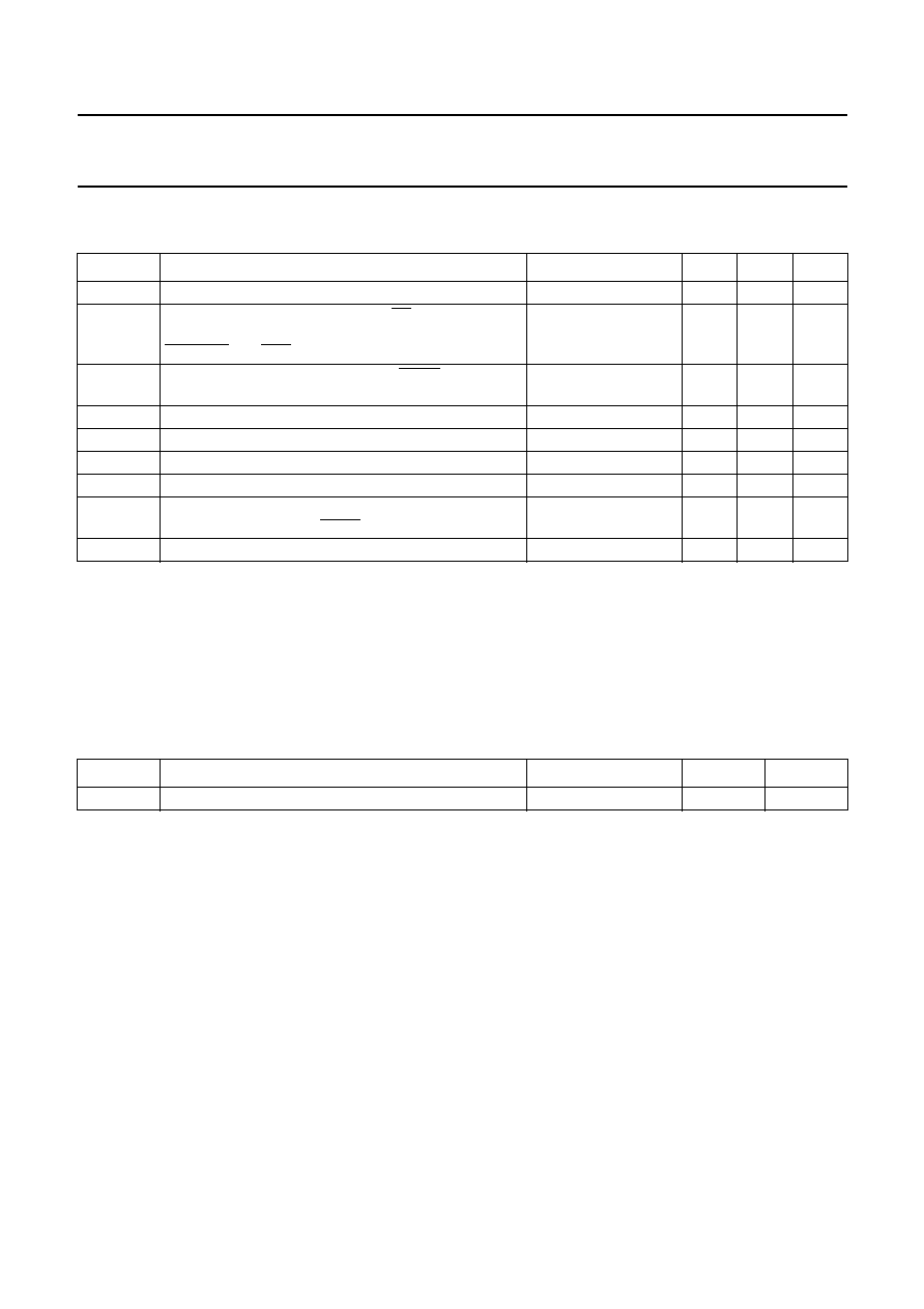
The following sequence then occurs (see Fig.5):
∑
CMDVCC is pulled LOW (t
0
)
∑
The voltage doubler is started (t
1
~ t
0
)
∑
V
CC
rises from 0 to 5 or 3V with a controlled slope
(t
2
= t
1
+
1
/
2
3T) (I/O, AUX1 and AUX2 follow V
CC
with a
slight delay); T is 64 times the period of the internal
oscillator, approximately 25
µ
s
∑
I/O, AUX1 and AUX2 are enabled (t
3
= t
1
+ 4T)
∑
CLK is applied to the C3 contact (t
4
)
∑
RST is enabled (t
5
= t
1
+ 7T).
The clock may be applied to the card in the following way:
Set RSTIN HIGH before setting CMDVCC LOW, and
reset it LOW between t
3
and t
5
; CLK will start at this
moment. RST will remain LOW until t
5
, where RST is
enabled to be the copy of RSTIN. After t
5
, RSTIN has no
further action on CLK. This is to allow a precise count of
CLK pulses before toggling RST.
If this feature is not needed, then CMDVCC may be set
LOW with RSTIN LOW. In this case, CLK will start at t
3
,
and after t
5
, RSTIN may be set HIGH in order to get the
Answer To Request (ATR) from the card.
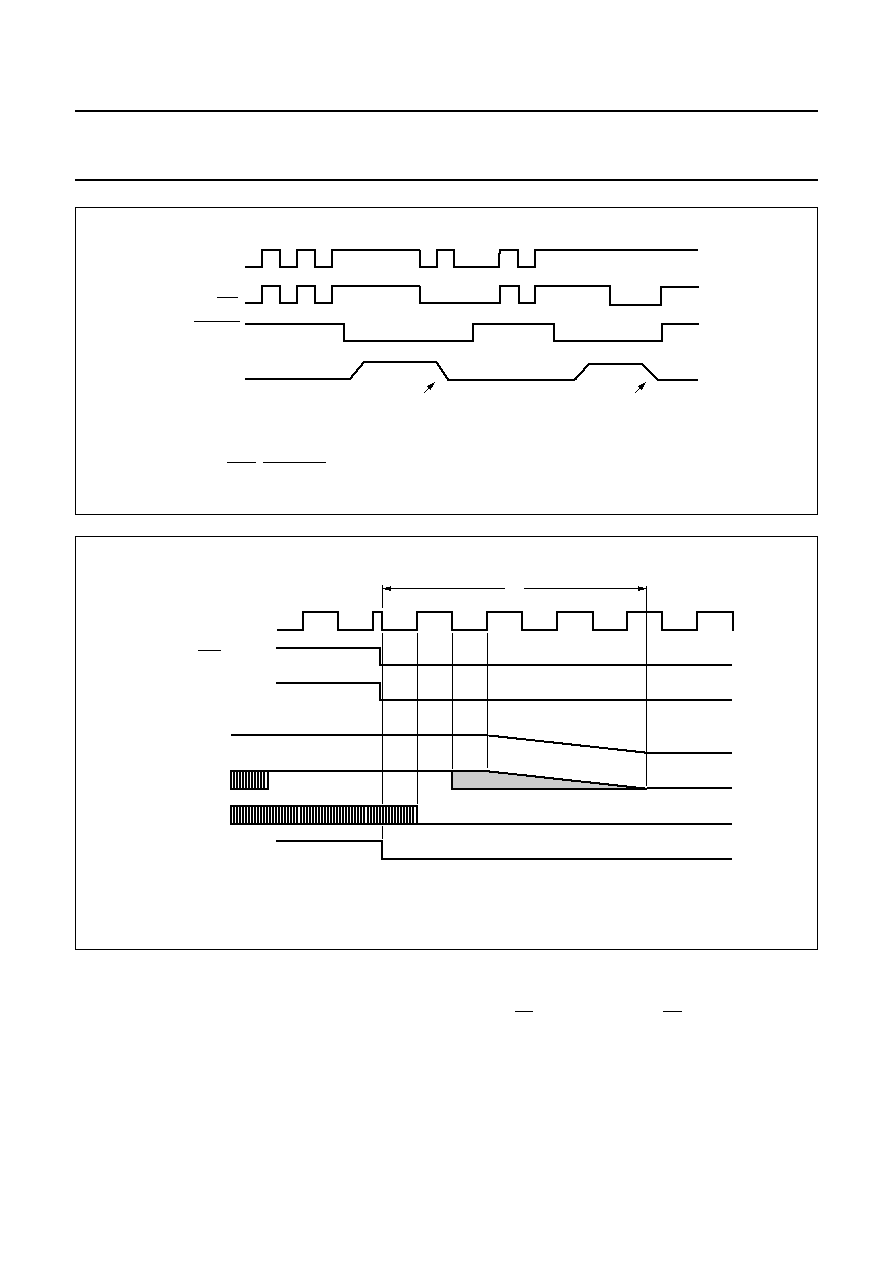
0
(2)
(1)
6
4
2
0
20
40
t (ns)
Vo
(V)
12
8
4
0
Io
(mA)
60
FCE661
Fig.4
I/O, AUX1 and AUX2 output voltage and
current as a function of time during a
LOW-to-HIGH transition.
(1) Current.
(2) Voltage.
2004 May 10
9
Philips Semiconductors
Product specification
IC card interface
TDA8004AT
FCE662
OSC_INT/64
CMDVCC
VUP
VCC
I/O
CLK
RSTIN
RST
high - Z
tact
t0
t1
t2
t3
t4
t5
ATR
Fig.5 Activation sequence.
Active state
When the activation sequence is completed, the
TDA8004AT will be in the active state. Data is exchanged
between the card and the microcontroller via the I/O lines.
The TDA8004AT is designed for cards without V
PP
(this is
the voltage required to program or erase the internal
non-volatile memory).
Depending on the layout and on the application test
conditions (for example with an additional 1 pF cross
capacitance between C2/C3 and C2/C7) it is possible that
C2 is polluted with high frequency noise from C3. In this
case, it will be necessary to connect a 220 pF capacitor
between C2 and CGND
.
It is recommended to:
1. Keep track C3 as far as possible from other tracks
2. Have straight connection between CGND and C5 (the
2 capacitors on C1 should be connected to this ground
track)
3. Avoid ground loops between CGND, PGND and GND
4. Decouple V
DDP
and V
DD
separately; if the 2 supplies
are the same in the application, then they should be
connected in star on the main track.
With all these layout precautions, noise should be at an
acceptable level, and jitter on C3 should be less than
100 ps. Refer to
Application Note AN97036 for specimen
layouts.
Deactivation sequence
When a session is completed, the microcontroller sets the
CMDVCC line to the HIGH state. The circuit then executes
an automatic deactivation sequence by counting the
sequencer back and ends in the inactive state (see Fig.6):
∑
RST goes LOW
(t
11
= t
10
)
∑
CLK is stopped LOW
(t
12
= t
11
+
1
/
2
T); where T is
approximately 25
µ
s
∑
I/O, AUX1 and AUX2 are output into high-impedance
state
(t
13
= t
11
+ T) (10 k
pull-up resistor connected
to V
CC
)
∑
V
CC
falls to zero
(t
14
= t
11
+
1
/
2
3T); the deactivation
sequence is completed when V
CC
reaches its inactive
state
∑
VUP falls to zero
(t
15
= t
11
+ 5T) and all card contacts
become low-impedance to GND; I/OUC, AUX1UC and
AUX2UC remain pulled up to V
DD
via a 10 k
resistor.

2004 May 10
10
Philips Semiconductors
Product specification
IC card interface
TDA8004AT
FCE663
CMDVCC
VUP
OSC_INT/64
VCC
I/O
CLK
RST
high - Z
tde
t10
t11
t12
t13
t14
t15
Fig.6 Deactivation sequence.
Fault detection
The following fault conditions are monitored by the circuit:
∑
Short-circuit or high current on V
CC
∑
Removing card during transaction
∑
V
DD
dropping
∑
Overheating.
There are two different cases (see Fig.7)
1. CMDVCC HIGH: (outside a card session) then, OFF is
LOW if the card is not in the reader, and HIGH if the
card is in the reader. A supply voltage drop on V
DD
is
detected by the supply supervisor which generates an
internal power-on reset pulse, but does not act upon
OFF. The card is not powered-up, so no short-circuit or
overheating is detected.
2. CMDVCC LOW: (within a card session) then, OFF falls
LOW if the card is extracted, or if a short-circuit has
occurred on V
CC
, or if the temperature on the IC has
become too high. As soon as the fault is detected, an
emergency deactivation is automatically performed
(see Fig.8).
When the system controller sets CMDVCC back to
HIGH, it may sense OFF again in order to distinguish
between a hardware problem or a card extraction. If a
supply voltage drop on V
DD
is detected whilst the card
is activated, then an emergency deactivation will be
performed, but OFF remains HIGH.
Depending on the type of card presence switch within the
connector (normally closed or normally open), and on the
mechanical characteristics of the switch, a bouncing may
occur on presence signals at card insertion or withdrawal.
There is no debounce feature in the device, so the
software has to take it into account; however, the detection
of card take off during active phase, which initiates an
automatic deactivation sequence is done on the first True/
False transition on PRES or PRES, and is memorized until
the system controller sets CMDVCC HIGH.
So, the software may take some time waiting for presence
switches to be stabilized without causing any delay on the
necessary fast and normalized deactivation sequence.
2004 May 10
11
Philips Semiconductors
Product specification
IC card interface
TDA8004AT
FCE665
OFF
CMDVCC
PRES
VCC
Deactivation caused by
cards withdrawal
Deactivation caused by
short circuit
Fig.7
Behaviour of OFF, CMDVCC, PRES and V
CC
(see also application note AN97036 for software decision
algorithm on OFF signal).
V
CC
regulator
The V
CC
buffer is able to deliver up to 65 mA continuously (at 5V if 5V/3V is HIGH or 3 V if 5V/3V is LOW). It has an
internal overload detection at approximately 90 mA.
This detection is internally filtered, allowing spurious current pulses up to 200 mA to be drawn by the card without causing
a deactivation (the average current value must stay below 65 mA).
For V
CC
accuracy reasons, a 100 nF capacitor with an ESR < 100 m
should be tied to CGND near pin 17, and a 100 nF
(or better 220 nF) with same ESR should be tied to CGND near to the C1 contact.
FCE664
I/O
CLK
RST
high - Z
tde
OSC_INT/64
OFF
PRES
VCC
t10
t11
t12
t13
t14
Fig.8 Emergency deactivation sequence.
2004 May 10
12
Philips Semiconductors
Product specification
IC card interface
TDA8004AT
LIMITING VALUES
In accordance with the Absolute Maximum Rating System (IEC 60134); note 1.
Note
1. All card contacts are protected against any short with any other card contact.
HANDLING
Every pin withstands the ESD test according to MIL-STD-883C class 3 for card contacts, class 2 for the remaining.
Method 3015 (HBM; 1500
; 100 pF) 3 pulses positive and 3 pulses negative on each pin referenced to ground.
THERMAL RESISTANCE
SYMBOL
PARAMETER
CONDITIONS
MIN.
MAX.
UNIT
V
DD
, V
DDP
supply voltage
-
0.3
+7
V
V
n1
voltage on pins XTAL1, XTAL2, 5V/3V, RSTIN,
AUX2UC, AUX1UC, I/OUC, CLKDIV1, CLKDIV2,
CMDVCC and OFF
-
0.3
+7
V
V
n2
voltage on card contact pins PRES, PRES, I/O, RST,
AUX1, AUX2 and CLK
-
0.3
+7
V
V
n3
voltage on pins VUP, S1 and S2
-
+9
V
T
stg
IC storage temperature
-
55
+125
∞
C
P
tot
continuous total power dissipation
T
amb
=
-
25 to +85
∞
C
-
0.56
W
T
j
junction temperature
-
150
∞
C
V
es1
electrostatic voltage on pins I/O, RST, V
CC
, AUX1,
CLK, AUX2, PRES and PRES
-
6
+6
kV
V
es2
electrostatic voltage on all other pins
-
2
+2
kV
SYMBOL
PARAMETER
CONDITIONS
VALUE
UNIT
R
th(j-a)
thermal resistance from junction to ambient
in free air
70
K/W
2004 May 10
13
Philips Semiconductors
Product specification
IC card interface
TDA8004AT
CHARACTERISTICS
V
DD
= 3.3 V; V
DDP
= 5 V; T
amb
= 25
∞
C; all parameters remain within limits but are only statistically tested for the
temperature range; f
XTAL
= 10 MHz; unless otherwise specified; all currents flowing into the IC are positive. When a
parameter is specified as a function of V
DD
or V
CC
it means their actual value at the moment of measurement.
SYMBOL
PARAMETER
CONDITIONS
MIN.
TYP.
MAX.
UNIT
Temperature
T
amb
ambient temperature
-
25
-
+85
∞
C
Supplies
V
DD
supply voltage
2.7
-
6.5
V
V
DDP
supply voltage for the voltage
doubler
4.5
5
6.5
V
V
o(VUP)
output voltage on pin VUP from
step-up converter
-
5.5
-
V
V
i(VUP)
input voltage to be applied on VUP
in order to block the step-up
converter
7
-
9
V
I
DD
supply current
inactive mode
-
-
1.2
mA
active mode; f
CLK
= f
XTAL
;
C
L
= 30 pF
-
-
1.5
mA
I
DDP
supply current step-up converter
inactive mode
-
-
0.1
mA
active mode; I
CC
= 0;
f
CLK
= f
XTAL
; C
L
= 30 pF
I
CC
= 0
-
-
18
mA
I
CC
= 65 mA
-
-
150
mA
V
th2
threshold voltage on V
DD
(falling)
2.2
-
2.4
V
V
hys(th2)
hysteresis on V
th2
50
-
150
mV
t
W
width of the internal ALARM pulse
6
-
20
ms
Card supply voltage; note 1
V
CC
output voltage including ripple
inactive mode
-
0.1
-
+0.1
V
inactive mode; I
CC
= 1 mA
-
0.1
-
+0.4
V
active mode;
I
CC
< 65 mA DC
5 V card
4.75
-
5.25
V
3 V card
2.85
-
3.15
V
active mode; single current
pulse of
-
100 mA; 2
µ
s
5 V card
4.65
-
5.25
V
3 V card
2.76
-
3.15
V
active mode; current pulses
of 40 nAs with
I
CC
< 200 mA; t < 400 ns
5 V card
4.65
-
5.25
V
3 V card
2.76
-
3.20
V
V
i(ripple)(p-p)
peak-to-peak ripple voltage on V
CC
from 20 kHz to 200 MHz
-
-
350
mV
2004 May 10
14
Philips Semiconductors
Product specification
IC card interface
TDA8004AT
I
CC
output current
from 0 to 5 or 3 V
-
-
65
mA
V
CC
short-circuit to ground
-
-
120
mA
SR
slew rate
up
0.09
0.18
0.27
V/
µ
s
down
0.09
0.21
0.27
V/
µ
s
Crystal connections (pins XTAL1 and XTAL2)
C
ext
external capacitors on pins
XTAL1 and XTAL2
depending on specification
of crystal or resonator used
-
-
15
pF
f
i(XTAL)
crystal input frequency
2
-
26
MHz
V
IH(XTAL)
HIGH-level input voltage on XTAL1
0.8V
DD
-
V
DD
+ 0.2 V
V
IL(XTAL)
LOW-level input voltage on XTAL1
-
0.3
-
+0.2V
DD
V
Data lines (pins I/O, I/OUC, AUX1, AUX2, AUX1UC and AUX2UC)
G
ENERAL
t
d(edge)
delay between falling edge on pins
I/OUC and I/O (or I/O and I/OUC)
and width of active pull-up pulse
-
200
-
ns
f
I/O(max)
maximum frequency on data lines
-
-
1
MHz
C
i
input capacitance on data lines
-
-
10
pF
D
ATA LINES
;
PINS
I/O, AUX1
AND
AUX2 (
WITH
10
K
PULL
-
UP RESISTOR CONNECTED TO
V
CC
)
V
OH
HIGH-level output voltage on data
lines
no DC load
0.9V
CC
-
V
CC
+ 0.1 V
I
OH
=
-
40
µ
A
0.75V
CC
-
V
CC
+ 0.1 V
V
OL
LOW-level output voltage on data
lines
I = 1 mA
-
-
300
mV
V
IH
HIGH-level input voltage on data
lines
1.8
-
V
CC
+ 0.3 V
V
IL
LOW-level input voltage on data
lines
-
0.3
-
+0.8
V
V
inactive
voltage on data lines outside a
session
no load
-
-
0.1
V
I
I/O
= 1 mA
-
-
0.3
V
I
edge
current from data lines when active
pull-up active
V
OH
= 0.9V
CC
; C
o
= 80 pF
-
1
-
-
mA
I
LIH
input leakage current HIGH on data
lines
V
IH
= V
CC
-
-
10
µ
A
I
IL
LOW-level input current on data
lines
V
IL
= 0 V
-
-
600
µ
A
t
t(DI)
input transition times on data lines
from V
IL
max to V
IH
min
-
-
1
µ
s
t
t(DO)
output transition times on data lines
C
o
= 80 pF, no DC load;
10% to 90% from 0 to V
CC
(see Fig.9)
-
-
0.1
µ
s
D
ATA LINES
;
PINS
I/OUC, AUX1UC
AND
AUX2UC (
WITH
10
K
PULL
-
UP RESISTOR CONNECTED TO
V
DD
)
V
OH
HIGH-level output voltage on data
lines
no DC load
0.9V
DD
-
V
DD
+ 0.2 V
I
OH
=
-
40
µ
A
0.75V
DD
-
V
DD
+ 0.2 V
SYMBOL
PARAMETER
CONDITIONS
MIN.
TYP.
MAX.
UNIT

2004 May 10
15
Philips Semiconductors
Product specification
IC card interface
TDA8004AT
V
OL
LOW-level output voltage on data
lines
I = 1 mA
-
-
300
mV
V
IH
HIGH-level input voltage on data
lines
0.7V
DD
-
V
DD
+ 0.3 V
V
IL
LOW-level input voltage on data
lines
0
-
0.3V
DD
V
I
LIH
input leakage current HIGH on data
lines
V
IH
= V
DD
-
-
10
µ
A
I
IL
LOW-level input on data lines
V
IL
= 0 V
-
-
600
µ
A
R
pu(int)
internal pull-up resistance between
data lines and V
DD
9
11
13
k
t
t(DI)
input transition times on data lines
from V
IL
max to V
IH
min
-
-
1
µ
s
t
t(DO)
output transition times on data lines
C
o
= 30 pF; 10% to 90%
from 0 to V
DD
(see Fig.9)
-
-
0.1
µ
s
Internal oscillator
f
osc(int)
frequency of internal oscillator
2.2
-
3.2
MHz
Reset output to the card (pin RST)
V
o(inactive)
output voltage in inactive mode
no load
0
-
0.1
V
I
o
= 1 mA
0
-
0.3
V
t
d(RSTIN-RST)
delay between pins RSTIN and RST RST enabled
-
-
2
µ
s
V
OL
LOW-level output voltage
I
OL
= 200
µ
A
0
-
0.3
V
V
OH
HIGH-level output voltage
I
OH
=
-
200
µ
A
0.9V
CC
-
V
CC
V
t
r
, t
f
rise and fall times
C
o
= 250 pF
-
-
0.1
µ
s
Clock output to the card (pin CLK)
V
o(inactive)
output voltage in inactive mode
no load
0
-
0.1
V
I
o
= 1 mA
0
-
0.3
V
V
OL
LOW-level output voltage
I
OL
= 200
µ
A
0
-
0.3
V
V
OH
HIGH-level output voltage
I
OH
=
-
200
µ
A
0.9V
CC
-
V
CC
V
f
CLK
card clock frequency
0
-
20
MHz
t
r
, t
f
rise and fall times
C
L
= 35 pF; note 2
-
-
8
ns
duty factor (except for f
XTAL
)
C
L
= 35 pF; note 2
45
-
55
%
SR
slew rate (rise and fall)
C
L
= 35 pF
0.2
-
-
V/ns
Logic inputs (pins CLKDIV, CLKDIV2,PRES, PRES, CMDVCC, RSTIN and 5V/3V); note 3
V
IL
LOW-level input voltage
-
-
0.3V
DD
V
V
IH
HIGH-level input voltage
0.7V
DD
-
-
V
I
LIL
input leakage current LOW
0 < V
IL
< V
DD
-
-
5
µ
A
I
LIH
input leakage current HIGH
0 < V
IH
< V
DD
-
-
5
µ
A
OFF output (pin OFF is an open-drain with an internal 20 k
pull-up resistor to V
DD
)
V
OL
LOW-level output voltage
I
OL
= 2 mA
-
-
0.4
V
SYMBOL
PARAMETER
CONDITIONS
MIN.
TYP.
MAX.
UNIT
2004 May 10
16
Philips Semiconductors
Product specification
IC card interface
TDA8004AT
Notes
1. To meet these specifications V
CC
should be decoupled to CGND using two ceramic multilayer capacitors of low ESR
with values of either 100 nF or one 100 nF and one 220 nF.
2. The transition times and duty factor definitions are shown in Fig.9;
3. PRES and CMDCC are active LOW; RSTIN and PRES are active HIGH; for CLKDIV1 and CLKDIV2 see Table 1.
V
OH
HIGH-level output voltage
I
OH
=
-
15
µ
A
0.75V
DD
-
-
V
Protections
T
sd
shut-down temperature
-
135
-
∞
C
I
CC(sd)
shut-down current at V
CC
-
-
110
mA
Timing
t
act
activation sequence duration
see Fig.5
-
180
220
µ
s
t
de
deactivation sequence duration
see Fig.6
60
80
100
µ
s
t
3
start of the window for sending CLK
to the card
see Fig.5
-
-
130
µ
s
t
5
end of the window for sending CLK
to the card
see Fig.5
140
-
-
µ
s
SYMBOL
PARAMETER
CONDITIONS
MIN.
TYP.
MAX.
UNIT
t
1
t
1
t
2
+
---------------
=
FCE666
10%
90%
90%
10%
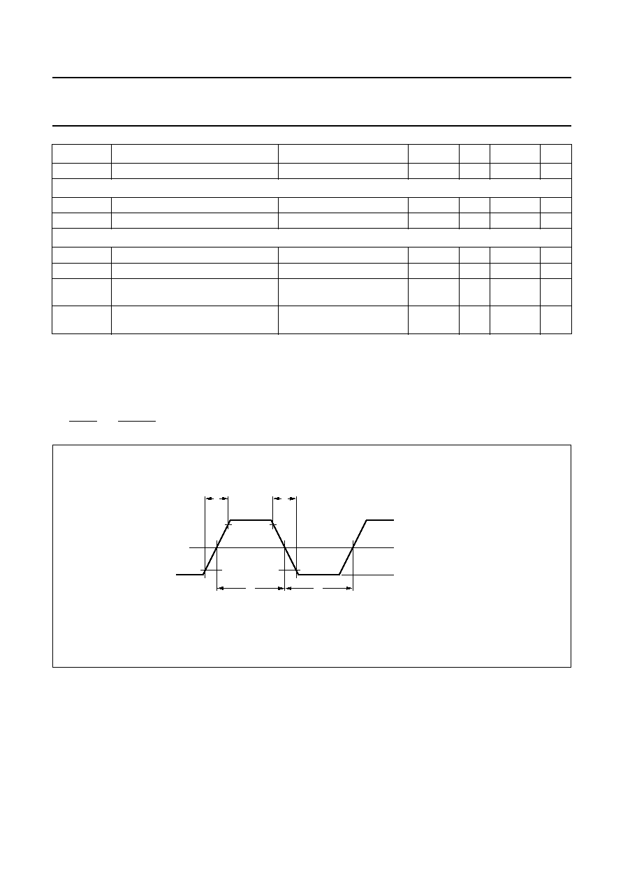
tr
tf
t1
t2
VOH
(VOH
+
VOL)/2
VOL
Fig.9 Definition of output transition times.

2004 May 10
17
Philips Semiconductors
Product specification
IC card interface
TDA8004AT
APPLICATION DIAGRAM
fce667
CLKDIV1
33 pF
TDA8004AT
AUX2UC
28
1
CLKDIV2
AUX1UC
27
2
5V/3V
XTAL2
26
3
GNDP
XTAL1
24
4
S2
OFF
23
5
V
DDP
GND
22
6
100 nF
+3.3 V
V
DD
21
RSTIN
20
CMDVCC
19
n.c.
18
V
CC
17
RST
16
CLK
15
3.3 V POWERED
MICROCONTROLLER
+3.3 V
S1
7
VUP
8
PRES
9
PRES
10
I/O
11
AUX2
12
AUX1
13
CGND
14
I/OUC
26
100
nF
10
µ
F
+5 V
100
nF
100
nF
V
DD
for the TDA8004 must be the same as controller
supply voltage, CLKDIV1, CLKDIV2, RSTIN, PRES,
PRES, AUXUC, I/OUC, AUX2UC, RFU1, CMDVCC,
OFF should be referenced to V
DD
and also XTAL1
if driven by external clock.
More application
information
on application report
AN97036
These capacitors
must be placed
near the IC and
have low ESR
(less than 1 cm).
CARD READ
(NORMALLY
CLOSED TYPE)
200 nF
C5
C1
C6
C2
C7
C3
C8
C4
K1
K2
100 nF
One 100 nF
with low ESR
near pin 17.
One 100 nF or 220 nF
with low ESR
near C1 contact
(less than 1 cm).
C3 should be routed
far from C2, C7, C4 and C8
and, better, surrounded
with ground tracks.
100 k
+3.3 V
Straight and short
connections between
CGND, C5 and
capacitors GND
(no loop).
Fig.10 Application diagram.

2004 May 10
18
Philips Semiconductors
Product specification
IC card interface
TDA8004AT
PACKAGE OUTLINE
UNIT
A
max.
A
1
A
2
A
3
b
p
c
D
(1)
E
(1)
(1)
e
H
E
L
L
p
Q
Z
y
w
v
REFERENCES
OUTLINE
VERSION
EUROPEAN
PROJECTION
ISSUE DATE
IEC
JEDEC
JEITA
mm
inches
2.65
0.3
0.1
2.45
2.25
0.49
0.36
0.32
0.23
18.1
17.7
7.6
7.4
1.27
10.65
10.00
1.1
1.0
0.9
0.4
8
0
o
o
0.25
0.1
DIMENSIONS (inch dimensions are derived from the original mm dimensions)
Note
1. Plastic or metal protrusions of 0.15 mm (0.006 inch) maximum per side are not included.
1.1
0.4
SOT136-1
X
14
28
w
M
A
A
1
A
2
b
p
D
H
E
L
p
Q
detail X
E
Z
c
L
v
M
A
e
15
1
(A )
3
A
y
0.25
075E06
MS-013
pin 1 index
0.1
0.012
0.004
0.096
0.089
0.019
0.014
0.013
0.009
0.71
0.69
0.30
0.29
0.05
1.4
0.055
0.419
0.394
0.043
0.039
0.035
0.016
0.01
0.25
0.01
0.004
0.043
0.016
0.01
0
5
10 mm
scale
SO28: plastic small outline package; 28 leads; body width 7.5 mm
SOT136-1
99-12-27
03-02-19

2004 May 10
19
Philips Semiconductors
Product specification
IC card interface
TDA8004AT
SOLDERING
Introduction to soldering surface mount packages
This text gives a very brief insight to a complex technology.
A more in-depth account of soldering ICs can be found in
our
"Data Handbook IC26; Integrated Circuit Packages"
(document order number 9398 652 90011).
There is no soldering method that is ideal for all surface
mount IC packages. Wave soldering can still be used for
certain surface mount ICs, but it is not suitable for fine pitch
SMDs. In these situations reflow soldering is
recommended.
Reflow soldering
Reflow soldering requires solder paste (a suspension of
fine solder particles, flux and binding agent) to be applied
to the printed-circuit board by screen printing, stencilling or
pressure-syringe dispensing before package placement.
Driven by legislation and environmental forces the
worldwide use of lead-free solder pastes is increasing.
Several methods exist for reflowing; for example,
convection or convection/infrared heating in a conveyor
type oven. Throughput times (preheating, soldering and
cooling) vary between 100 and 200 seconds depending
on heating method.
Typical reflow peak temperatures range from
215 to 270
∞
C depending on solder paste material. The
top-surface temperature of the packages should
preferably be kept:
∑
below 225
∞
C (SnPb process) or below 245
∞
C (Pb-free
process)
≠ for all BGA, HTSSON-T and SSOP-T packages
≠ for packages with a thickness
2.5 mm
≠ for packages with a thickness < 2.5 mm and a
volume
350 mm
3
so called thick/large packages.
∑
below 240
∞
C (SnPb process) or below 260
∞
C (Pb-free
process) for packages with a thickness < 2.5 mm and a
volume < 350 mm
3
so called small/thin packages.
Moisture sensitivity precautions, as indicated on packing,
must be respected at all times.
Wave soldering
Conventional single wave soldering is not recommended
for surface mount devices (SMDs) or printed-circuit boards
with a high component density, as solder bridging and
non-wetting can present major problems.
To overcome these problems the double-wave soldering
method was specifically developed.
If wave soldering is used the following conditions must be
observed for optimal results:
∑
Use a double-wave soldering method comprising a
turbulent wave with high upward pressure followed by a
smooth laminar wave.
∑
For packages with leads on two sides and a pitch (e):
≠ larger than or equal to 1.27 mm, the footprint
longitudinal axis is preferred to be parallel to the
transport direction of the printed-circuit board;
≠ smaller than 1.27 mm, the footprint longitudinal axis
must be parallel to the transport direction of the
printed-circuit board.
The footprint must incorporate solder thieves at the
downstream end.
∑
For packages with leads on four sides, the footprint must
be placed at a 45
∞
angle to the transport direction of the
printed-circuit board. The footprint must incorporate
solder thieves downstream and at the side corners.
During placement and before soldering, the package must
be fixed with a droplet of adhesive. The adhesive can be
applied by screen printing, pin transfer or syringe
dispensing. The package can be soldered after the
adhesive is cured.
Typical dwell time of the leads in the wave ranges from
3 to 4 seconds at 250
∞
C or 265
∞
C, depending on solder
material applied, SnPb or Pb-free respectively.
A mildly-activated flux will eliminate the need for removal
of corrosive residues in most applications.
Manual soldering
Fix the component by first soldering two
diagonally-opposite end leads. Use a low voltage (24 V or
less) soldering iron applied to the flat part of the lead.
Contact time must be limited to 10 seconds at up to
300
∞
C.
When using a dedicated tool, all other leads can be
soldered in one operation within 2 to 5 seconds between
270 and 320
∞
C.
2004 May 10
20
Philips Semiconductors
Product specification
IC card interface
TDA8004AT
Suitability of surface mount IC packages for wave and reflow soldering methods
Notes
1. For more detailed information on the BGA packages refer to the
"(LF)BGA Application Note" (AN01026); order a copy
from your Philips Semiconductors sales office.
2. All surface mount (SMD) packages are moisture sensitive. Depending upon the moisture content, the maximum
temperature (with respect to time) and body size of the package, there is a risk that internal or external package
cracks may occur due to vaporization of the moisture in them (the so called popcorn effect). For details, refer to the
Drypack information in the
"Data Handbook IC26; Integrated Circuit Packages; Section: Packing Methods".
3. These transparent plastic packages are extremely sensitive to reflow soldering conditions and must on no account
be processed through more than one soldering cycle or subjected to infrared reflow soldering with peak temperature
exceeding 217
∞
C
±
10
∞
C measured in the atmosphere of the reflow oven. The package body peak temperature
must be kept as low as possible.
4. These packages are not suitable for wave soldering. On versions with the heatsink on the bottom side, the solder
cannot penetrate between the printed-circuit board and the heatsink. On versions with the heatsink on the top side,
the solder might be deposited on the heatsink surface.
5. If wave soldering is considered, then the package must be placed at a 45
∞
angle to the solder wave direction.
The package footprint must incorporate solder thieves downstream and at the side corners.
6. Wave soldering is suitable for LQFP, TQFP and QFP packages with a pitch (e) larger than 0.8 mm; it is definitely not
suitable for packages with a pitch (e) equal to or smaller than 0.65 mm.
7. Wave soldering is suitable for SSOP, TSSOP, VSO and VSSOP packages with a pitch (e) equal to or larger than
0.65 mm; it is definitely not suitable for packages with a pitch (e) equal to or smaller than 0.5 mm.
8. Image sensor packages in principle should not be soldered. They are mounted in sockets or delivered pre-mounted
on flex foil. However, the image sensor package can be mounted by the client on a flex foil by using a hot bar
soldering process. The appropriate soldering profile can be provided on request.
9. Hot bar or manual soldering is suitable for PMFP packages.
PACKAGE
(1)
SOLDERING METHOD
WAVE
REFLOW
(2)
BGA, HTSSON..T
(3)
, LBGA, LFBGA, SQFP, SSOP..T
(3)
, TFBGA,
USON, VFBGA
not suitable
suitable
DHVQFN, HBCC, HBGA, HLQFP, HSO, HSOP, HSQFP, HSSON,
HTQFP, HTSSOP, HVQFN, HVSON, SMS
not suitable
(4)
suitable
PLCC
(5)
, SO, SOJ
suitable
suitable
LQFP, QFP, TQFP
not recommended
(5)(6)
suitable
SSOP, TSSOP, VSO, VSSOP
not recommended
(7)
suitable
CWQCCN..L
(8)
, PMFP
(9)
, WQCCN..L
(8)
not suitable
not suitable
2004 May 10
21
Philips Semiconductors
Product specification
IC card interface
TDA8004AT
DATA SHEET STATUS
Notes
1. Please consult the most recently issued data sheet before initiating or completing a design.
2. The product status of the device(s) described in this data sheet may have changed since this data sheet was
published. The latest information is available on the Internet at URL http://www.semiconductors.philips.com.
3. For data sheets describing multiple type numbers, the highest-level product status determines the data sheet status.
LEVEL
DATA SHEET
STATUS
(1)
PRODUCT
STATUS
(2)(3)
DEFINITION
I
Objective data
Development
This data sheet contains data from the objective specification for product
development. Philips Semiconductors reserves the right to change the
specification in any manner without notice.
II
Preliminary data Qualification
This data sheet contains data from the preliminary specification.
Supplementary data will be published at a later date. Philips
Semiconductors reserves the right to change the specification without
notice, in order to improve the design and supply the best possible
product.
III
Product data
Production
This data sheet contains data from the product specification. Philips
Semiconductors reserves the right to make changes at any time in order
to improve the design, manufacturing and supply. Relevant changes will
be communicated via a Customer Product/Process Change Notification
(CPCN).
DEFINITIONS
Short-form specification
The data in a short-form
specification is extracted from a full data sheet with the
same type number and title. For detailed information see
the relevant data sheet or data handbook.
Limiting values definition
Limiting values given are in
accordance with the Absolute Maximum Rating System
(IEC 60134). Stress above one or more of the limiting
values may cause permanent damage to the device.
These are stress ratings only and operation of the device
at these or at any other conditions above those given in the
Characteristics sections of the specification is not implied.
Exposure to limiting values for extended periods may
affect device reliability.
Application information
Applications that are
described herein for any of these products are for
illustrative purposes only. Philips Semiconductors make
no representation or warranty that such applications will be
suitable for the specified use without further testing or
modification.
DISCLAIMERS
Life support applications
These products are not
designed for use in life support appliances, devices, or
systems where malfunction of these products can
reasonably be expected to result in personal injury. Philips
Semiconductors customers using or selling these products
for use in such applications do so at their own risk and
agree to fully indemnify Philips Semiconductors for any
damages resulting from such application.
Right to make changes
Philips Semiconductors
reserves the right to make changes in the products -
including circuits, standard cells, and/or software -
described or contained herein in order to improve design
and/or performance. When the product is in full production
(status `Production'), relevant changes will be
communicated via a Customer Product/Process Change
Notification (CPCN). Philips Semiconductors assumes no
responsibility or liability for the use of any of these
products, conveys no licence or title under any patent,
copyright, or mask work right to these products, and
makes no representations or warranties that these
products are free from patent, copyright, or mask work
right infringement, unless otherwise specified.

© Koninklijke Philips Electronics N.V. 2004
SCA76
All rights are reserved. Reproduction in whole or in part is prohibited without the prior written consent of the copyright owner.
The information presented in this document does not form part of any quotation or contract, is believed to be accurate and reliable and may be changed
without notice. No liability will be accepted by the publisher for any consequence of its use. Publication thereof does not convey nor imply any license
under patent- or other industrial or intellectual property rights.
Philips Semiconductors ≠ a worldwide company
Contact information
For additional information please visit http://www.semiconductors.philips.com.
Fax: +31 40 27 24825
For sales offices addresses send e-mail to: sales.addresses@www.semiconductors.philips.com.
Printed in The Netherlands
R63/02/pp
22
Date of release:
2004 May 10
Document order number:
9397 750 13142