 | –≠–ª–µ–∫—Ç—Ä–æ–Ω–Ω—ã–π –∫–æ–º–ø–æ–Ω–µ–Ω—Ç: TDA8261 | –°–∫–∞—á–∞—Ç—å:  PDF PDF  ZIP ZIP |
Document Outline
- FEATURES
- APPLICATIONS
- GENERAL DESCRIPTION
- QUICK REFERENCE DATA
- ORDERING INFORMATION
- BLOCK DIAGRAM
- PINNING
- FUNCTIONAL DESCRIPTION
- PROGRAMMING
- LIMITING VALUES
- THERMAL CHARACTERISTICS
- HANDLING
- CHARACTERISTICS
- APPLICATION INFORMATION
- PACKAGE OUTLINE
- SOLDERING
- DATA SHEET STATUS
- DEFINITIONS
- DISCLAIMERS

DATA SHEET
Preliminary specification
2003 May 28
INTEGRATED CIRCUITS
TDA8261TW
Satellite Zero-IF QPSK/8PSK
downconverter with PLL
synthesizer

2003 May 28
2
Philips Semiconductors
Preliminary specification
Satellite Zero-IF QPSK/8PSK
downconverter with PLL synthesizer
TDA8261TW
FEATURES
∑
Direct conversion Quadrature Phase Shift Keying
(QPSK) and 8PSK demodulation (Zero-IF)
∑
950 to 2175 MHz frequency range
∑
High-level asymmetrical RF input
∑
0 to 50 dB variable gain on RF input
∑
Loop-controlled 0
∞
to 90
∞
phase shifter
∑
High AGC linearity (<1 dB per bit with an 8-bit DAC),
AGC between 0 and 3 V
∑
External baseband filters for In-phase (I) and
Quadrature (Q) signal paths
∑
I
2
C-bus controlled PLL frequency synthesizer
∑
Low phase noise
∑
Operation from a 4 MHz crystal (allowing the use of an
SMD crystal)
∑
Five frequency steps from 125 kHz to 2 MHz
∑
Crystal frequency output to drive demodulator IC
∑
Compatible with 5, 3.3 and 2.5 V I
2
C-bus
∑
Fully compatible and easy to interface with digital
satellite demodulators of the Philips Semiconductors
family
∑
5 V DC supply voltage
∑
32-pin high heat-dissipation package.
APPLICATIONS
∑
Direct Broadcasting Satellite (DBS) QPSK
demodulation
∑
Digital Video Broadcasting (DVB) QPSK demodulation
∑
BS digital 8PSK demodulation.
GENERAL DESCRIPTION
The direct conversion QPSK demodulator is the front-end
receiver dedicated to digital TV broadcasting, satisfying
both DVB and DBS TV standards. The wide range
oscillator (from 950 to 2175 MHz) covers the American,
European and Asian satellite bands, as well as the
Satellite Master Antennae (SMA) TV US standard.
The Zero-IF concept discards traditional IF filtering and
intermediate conversion techniques. It also simplifies the
signal path.
Optimum signal level is guaranteed by gain controlled
amplifiers in the RF path. The 0 to 50 dB variable gain is
controlled by the signal returned from the Satellite
Demodulator and Decoder (SDD) and applied to
pin AGCIN.
The PLL synthesizer is built on a dual-loop concept. The
first loop controls a fully integrated L-band oscillator, using
the LC VCO as a reference which runs at a quarter of the
synthesized frequency.
The second loop controls the tuning voltage of the VCO
and improves the phase noise of the carrier within the loop
bandwidth. The step size is equal to the comparison
frequency. The input of the main divider of the PLL
synthesizer is connected internally to the VCO output.
The comparison frequency of the second loop is obtained
from an oscillator driven by an external 4 MHz crystal. The
4 MHz output available at pin XTOUT may be used to drive
the crystal inputs of the SDD, saving an additional crystal
in the application.
Both the divided and the comparison frequencies of the
second loop are compared in a fast phase detector which
drives the charge pump. The TDA8261TW includes a loop
amplifier with an internal high-voltage transistor to drive an
external 33 V tuning voltage.
Control data is entered via the I
2
C-bus. The I
2
C-bus
voltage can be 5, 3.3 or 2.5 V, allowing compatibility with
most of the existing microcontrollers.
A 5-byte frame is required to address the device and to
program the main divider ratio, the reference divider ratio,
the charge pump current and the operating mode.
A flag is set when the loop is `in-lock'. This flag can be read
during read operations, as well as the Power-On Reset
(POR) flag.
The device has four selectable I
2
C-bus addresses. The
selection is done by applying a specific voltage to pin AS.
This feature gives the possibility to use up to four
TDA8261TW ICs in the same system.
2003 May 28
3
Philips Semiconductors
Preliminary specification
Satellite Zero-IF QPSK/8PSK
downconverter with PLL synthesizer
TDA8261TW
Performance summary
TDA8261TW performance:
∑
Noise figure at maximum gain = +18 dB
∑
High linearity; IP2 = +19 dBm and IP3 = +14 dBm
∑
Low phase noise on baseband outputs:
-
78 dBc/Hz
(f
offset
= 1 and 10 kHz; f
COMP
= 1 MHz)
∑
0 to 50 dB variable gain with AGC control
∑
AGC linearity <1 dB/bit with an 8-bit DAC
∑
Maximum I-to-Q amplitude mismatch = 1 dB
∑
Maximum I-to-Q phase mismatch = 3
∞
∑
Signal rates from 1 to 45 Msymbol/s (depending on the
external filter).
System performance, for example, in a tuner application
with the TDA8261TW placed after a low-cost discrete
LNA:
∑
Noise figure at maximum gain = 8 dB
∑
High linearity; IP2 = 15 dBm and IP3 = 5 dBm
∑
0 to 50 dB variable gain with AGC control.
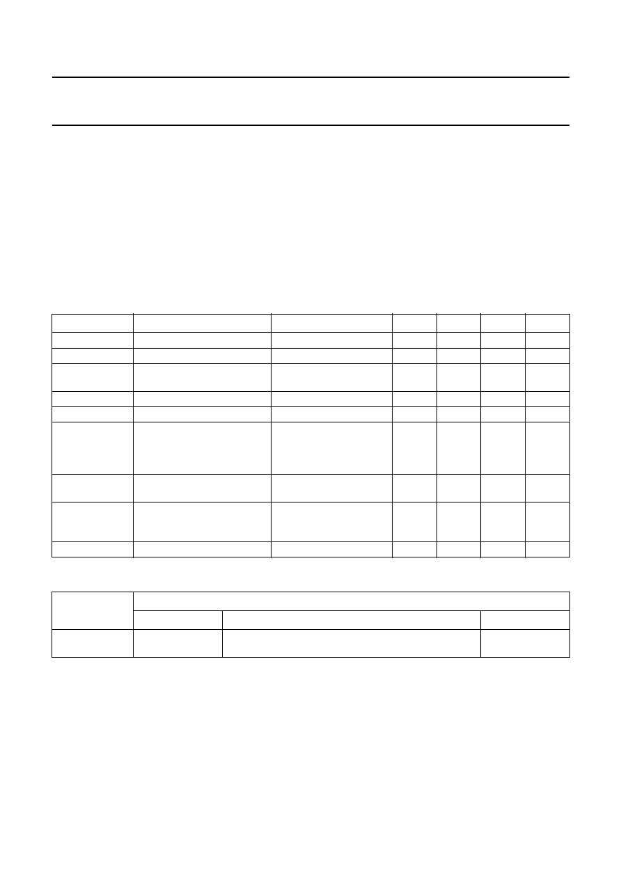
QUICK REFERENCE DATA
ORDERING INFORMATION
SYMBOL
PARAMETER
CONDITIONS
MIN.
TYP.
MAX.
UNIT
V
CC
supply voltage
4.75
5.0
5.25
V
I
CC
supply current
-
130
-
mA
V
o(p-p)
output voltage
(peak-to-peak value)
-
750
-
mV
quadrature error
-
-
3
deg
f
osc
oscillator frequency
950
-
2175
MHz
n
phase noise on baseband
outputs
f
offset
= 1 and 10 kHz;
f
COMP
= 1 MHz with
appropriate loop filter and
charge pump
-
-
-
78
dBc/Hz
G
v
dynamic range of voltage gain from pins RFA or RFB to
pins IBBOUT or QBBOUT
48
50
-
dB
V
XTOUT(p-p)
crystal oscillator output
voltage on pin XTOUT
(peak-to-peak value)
T2 = 1; T1 = 0; T0 = 0;
driving a load of
C
L
= 10 pF; R
L
= 1 M
400
500
-
mV
T
amb
ambient temperature
-
20
-
+85
∞
C
TYPE NUMBER
PACKAGE
NAME
DESCRIPTION
VERSION
TDA8261TW
HTSSOP32
plastic, heatsink thin shrink small outline package;
32 leads; body width 6.1 mm; lead pitch 0.65 mm
SOT549-1

2003 May 28
4
Philips Semiconductors
Preliminary specification
Satellite Zero-IF QPSK/8PSK
downconverter with PLL synthesizer
TDA8261TW
BLOCK DIAGRAM
handbook, full pagewidth
21
15
6
18
13
20
11
10
7
8
25
22
3
4
9
AGC
CONTROL
VCO
fDIV
fXTAL
fCOMP
FAST PHASE/
FREQUENCY
COMPARATOR
DIGITAL PHASE
COMPARATOR
REFERENCE
DIVIDER
POWER-ON
RESET
CONTROL LOGIC
AND LATCH
OSCILLATOR
CHARGE PUMP
DIVIDE-BY-4
15-BIT DIVIDER
33 V
AMP
12
14
19
17
16
32
27
28
5
I
Q
integrated
oscillator
23
24
2
1
I
2
C-BUS
30
31
26
29
TDA8261TW
MBL859
XTOUT
SDA
SCL
AS
CP
VT
BVS
VCC(VCO)
TKA
TKB
VCOGND
BIASN2
IOUT
BBGND2
IBBIN
IBBOUT
XT1
XT2
VCC(PLL)
PLLGND
AGCIN
BIASN1
RFGND1
VCC(RF)
RFA
RFB
RFGND2
QOUT
BBGND1
QBBIN
VCC(BB)
QBBOUT
Fig.1 Block diagram.

2003 May 28
5
Philips Semiconductors
Preliminary specification
Satellite Zero-IF QPSK/8PSK
downconverter with PLL synthesizer
TDA8261TW
PINNING
SYMBOL
PIN
DESCRIPTION
XT1
1
4 MHz crystal oscillator input 1
XT2
2
4 MHz crystal oscillator input 2
V
CC(PLL)
3
supply voltage for PLL circuit (5 V)
PLLGND
4
ground for PLL circuit
AGCIN
5
AGC input from satellite
demodulator and decoder
BIASN1
6
RF isolation input 1 (5 V)
RFGND1
7
ground 1 for RF circuit
V
CC(RF)
8
supply voltage for RF stage (5 V)
RFA
9
RF signal input A
RFB
10
RF signal input B
RFGND2
11
ground 2 for RF circuit
QOUT
12
quadrature output for external
filtering
BBGND1
13
ground 1 for baseband stage
QBBIN
14
quadrature baseband input after
external filtering
V
CC(BB)
15
supply voltage for baseband stage
(5 V)
QBBOUT
16
quadrature baseband output to
satellite demodulator and decoder
IBBOUT
17
in-phase baseband output to
satellite demodulator and decoder
BIASN2
18
RF isolation input 2 (5 V)
IBBIN
19
in-phase baseband input after
external filtering
BBGND2
20
ground 2 for baseband stage
IOUT
21
in-phase output for external filtering
VCOGND
22
ground for VCO circuit
TKB
23
VCO tank circuit input B
TKA
24
VCO tank circuit input A
V
CC(VCO)
25
supply voltage for VCO circuit (5 V)
BVS
26
bus voltage select input
VT
27
tuning voltage output for VCO
CP
28
charge pump output
AS
29
address selection input
SCL
30
I
2
C-bus clock input
SDA
31
I
2
C-bus data input and output
XTOUT
32
4 MHz crystal oscillator output to
satellite demodulator and decoder
handbook, halfpage
TDA8261TW
MBL855
1
2
3
4
5
6
7
8
9
10
11
12
13
14
15
16
XT1
XT2
VCC(PLL)
PLLGND
AGCIN
BIASN1
RFGND1
VCC(RF)
RFA
RFB
RFGND2
QOUT
BBGND1
QBBIN
VCC(BB)
QBBOUT
XTOUT
SDA
SCL
AS
CP
VT
BVS
VCC(VCO)
TKA
TKB
VCOGND
IOUT
BBGND2
IBBIN
BIASN2
IBBOUT
32
31
30
29
28
27
26
25
24
23
22
21
20
19
18
17
Fig.2 Pin configuration.