Document Outline
- FEATURES
- GENERAL DESCRIPTION
- QUICK REFERENCE DATA
- ORDERING INFORMATION
- BLOCK DIAGRAM
- PINNING
- FUNCTIONAL DESCRIPTION
- I 2 C-bus interface
- Vmax
- DACs
- LIMITING VALUES
- QUALITY SPECIFICATION
- THERMAL CHARACTERISTICS
- CHARACTERISTICS
- TEST AND APPLICATION INFORMATION
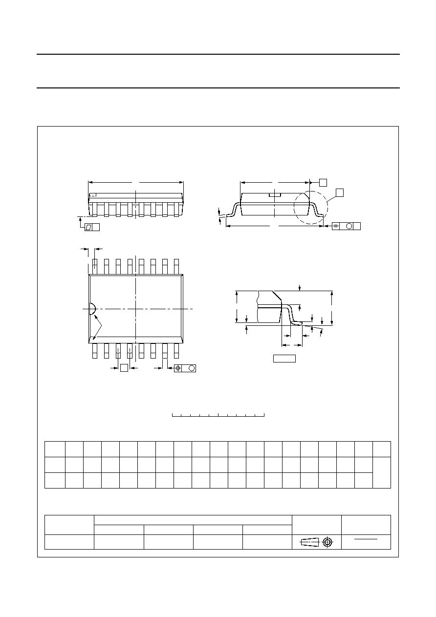
- PACKAGE OUTLINES
- SOT38-1
- SOT162-1
- SOT163-1
- SOLDERING
- DEFINITIONS
- LIFE SUPPORT APPLICATIONS
- PURCHASE OF PHILIPS I C COMPONENTS
DATA SHEET
Product specification
Supersedes data of March 1991
File under Integrated Circuits, IC01
1999 Apr 29
INTEGRATED CIRCUITS
TDA8444; TDA8444T;
TDA8444AT
Octuple 6-bit DACs with I
2
C-bus
1999 Apr 29
2
Philips Semiconductors
Product specification
Octuple 6-bit DACs with I
2
C-bus
TDA8444; TDA8444T;
TDA8444AT
FEATURES
∑
Eight DACs with 6-bit resolution
∑
Adjustable common output swing
∑
Push-pull outputs
∑
Outputs short-circuit protected
∑
Three programmable slave address bits
∑
Large supply voltage range
∑
Low temperature coefficient.
GENERAL DESCRIPTION
The interface circuit is a bipolar IC in a DIP16, SO16, or
SO20 package made in an I2L-compatible 18 V process.
The TDA8444 contains eight programmable 6-bit DAC
outputs, an I
2
C-bus slave receiver with three (two for
SO16) programmable address bits and one input (V
MAX
) to
set the maximum output voltage. Each DAC can be
programmed separately by a 6-bit word to 64 values, but
V
MAX
determines the maximum output voltage for all
DACs. The resolution will be approximately
1
/
64
V
MAX
.
At power-on all DACs are set to their lowest value.
QUICK REFERENCE DATA
ORDERING INFORMATION
SYMBOL
PARAMETER
CONDITIONS
MIN.
TYP.
MAX.
UNIT
V
CC
supply voltage
4.5
12
13.2
V
I
CC
supply current
V
CC
= 12 V
-
14
-
mA
P
power dissipation
-
170
-
mW
V
VMAX
input effective voltage
1
-
V
CC
-
2.0
V
V
o(DACn)
DAC output voltage
V
MAX
= V
CC
0.1
-
V
CC
-
0.5
V
V
o(DACn)(max)
maximum DAC output voltage
1 < V
MAX
< V
CC
-
2.0
-
V
MAX
+ 0.3
-
V
I
source(min)
minimum DAC source current
data = 1FH
2
-
-
mA
I
sink(min)
minimum DAC sink current
data = 1FH
2
-
-
mA
TYPE
NUMBER
PACKAGE
NAME
DESCRIPTION
VERSION
TDA8444
DIP16
plastic dual in-line package; 16 leads (300 mil); long body
SOT38-1
TDA8444T
SO16
plastic small outline package; 16 leads; body width 7.5 mm
SOT162-1
TDA8444AT
SO20
plastic small outline package; 20 leads; body width 7.5 mm
SOT163-1
1999 Apr 29
3
Philips Semiconductors
Product specification
Octuple 6-bit DACs with I
2
C-bus
TDA8444; TDA8444T;
TDA8444AT
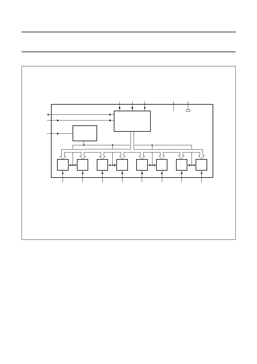
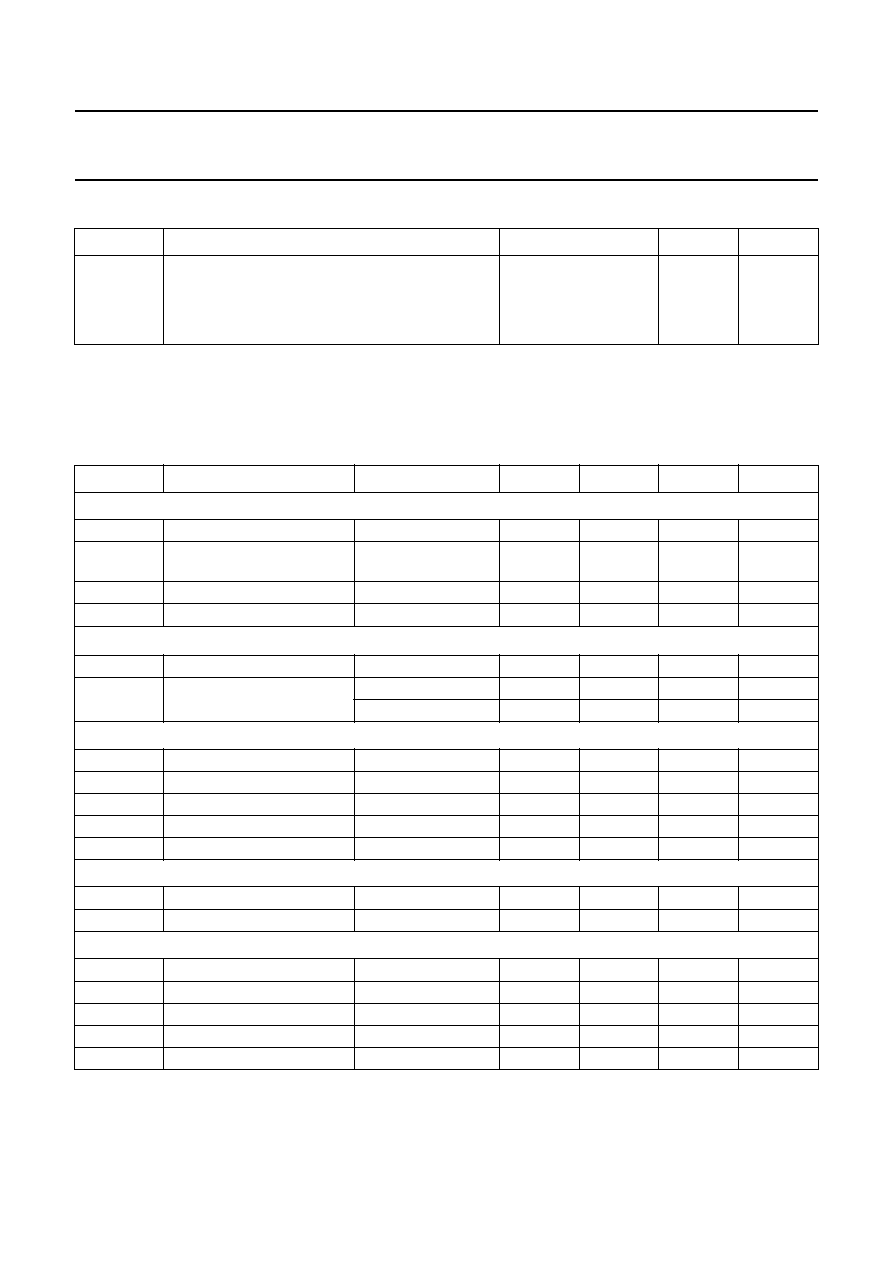
BLOCK DIAGRAM
Fig.1 Block diagram.
handbook, full pagewidth
MGH513
REFERENCE
VOLTAGE
GENERATOR
DAC0
DAC0
9
DAC1
DAC1
10
DAC2
DAC2
11
DAC3
DAC3
12
DAC4
DAC4
13
DAC5
DAC5
14
DAC6
DAC6
15
DAC7
DAC7
16
A0
A1
A2
5
6
7
1
8
SDA
SCL
3
4
VMAX
2
VCC
VEE
TDA8444
I
2
C BUS
SLAVE RECEIVER
1999 Apr 29
4
Philips Semiconductors
Product specification
Octuple 6-bit DACs with I
2
C-bus
TDA8444; TDA8444T;
TDA8444AT
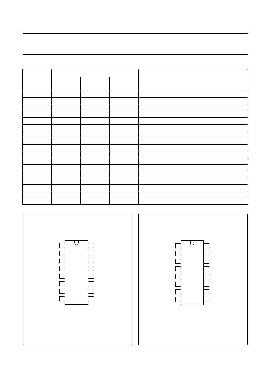
PINNING
SYMBOL
PIN
DESCRIPTION
TDA8444
(DIP16)
TDA8444T
(SO16)
TDA8444AT
(SO20)
V
CC
1
1
1
supply voltage
V
MAX
2
2
2
control input for DAC maximum output voltage
SDA
3
3
3
I
2
C-bus serial data input/output
SCL
4
4
4
I
2
C-bus serial clock
A0
5
6
7
programmable address bit 0 for I
2
C-bus slave receiver
A1
6
7
8
programmable address bit 1 for I
2
C-bus slave receiver
A2
7
-
9
programmable address bit 2 for I
2
C-bus slave receiver
V
EE
8
8
10
ground
DAC0
9
9
11
analog voltage output 0
DAC1
10
10
13
analog voltage output 1
DAC2
11
11
14
analog voltage output 2
DAC3
12
12
15
analog voltage output 3
DAC4
13
13
16
analog voltage output 4
DAC5
14
14
17
analog voltage output 5
DAC6
15
15
18
analog voltage output 6
DAC7
16
16
20
analog voltage output 7
n.c.
-
5
5, 6, 12, 19
not connected
Fig.2 Pin configuration (TDA8444; DIP16).
handbook, halfpage
TDA8444
MGH512
1
2
3
4
5
6
7
8
16
15
14
13
12
11
10
9
VEE
DAC0
A2
DAC1
A1
DAC2
DAC3
DAC4
DAC5
DAC6
DAC7
A0
SCL
SDA
VMAX
VCC
Fig.3 Pin configuration (TDA8444T; SO16).
handbook, halfpage
TDA8444T
MGL531
1
2
3
4
5
6
7
8
16
15
14
13
12
11
10
9
VEE
DAC0
A1
DAC1
A0
DAC2
DAC3
DAC4
DAC5
DAC6
DAC7
n.c.
SCL
SDA
VMAX
VCC
1999 Apr 29
5
Philips Semiconductors
Product specification
Octuple 6-bit DACs with I
2
C-bus
TDA8444; TDA8444T;
TDA8444AT
Fig.4 Pin configuration (TDA8444AT; SO20).
handbook, halfpage
TDA8444AT
MGL532
1
2
3
4
5
6
7
8
9
10
VCC
VMAX
SDA
SCL
n.c.
n.c.
A0
A1
A2
VEE
DAC7
n.c.
DAC6
DAC5
DAC4
DAC3
DAC2
DAC1
n.c.
DAC0
20
19
18
17
16
15
14
13
12
11
FUNCTIONAL DESCRIPTION
I
2
C-bus interface
The I
2
C-bus interface is a receive-only slave, which accepts data according the format shown in Table 1.
Table 1
I
2
C-bus format (see note 1)
Note
1. S = START condition; A2 to A0 = programmable address bits; A = Acknowledge; I3 to I0 = Instruction bits;
SD to SA = subaddress bits; X = don't care; D5 to D0 = data bits; P = STOP condition.
Valid addresses are:
TDA8444 and TDA8444AT: 40H, 42H, 44H, 46H, 48H, 4AH, 4CH and 4EH
TDA8444T: 48H, 4AH, 4CH and 4EH (A2 is always logic 1).
All other addresses cannot be acknowledged by the circuit. The actual slave address depends on the programmable
address bits A2, A1 and A0. This way up to eight circuits can be used on one I
2
C-bus.
Valid instructions are: 00H to 0FH; F0H to FFH.
S
0 1 0 0 A2 A1 A0 0
A
I3 I2 I1 I0 SD SC SB SA
A
X X D5 D4 D3 D2 D1 D0
A
P

1999 Apr 29
6
Philips Semiconductors
Product specification
Octuple 6-bit DACs with I
2
C-bus
TDA8444; TDA8444T;
TDA8444AT
The circuit will not react to other combinations of the
4 instruction bits I3 to I0 than 0 or F, but will still generate
an acknowledge. The difference between
instruction 0 and F is only important when more than one
data byte is sent within one transmission. Instruction 0
causes the data bytes to be written into the DAC-latches
with consecutive subaddresses starting with the
subaddress given in the instruction byte (auto-increment of
subaddress), while instruction F will cause a consecutive
writing of the data bytes into the same DAC-latch whose
subaddress was given in the instruction byte. In case of
only one data byte the DAC-latch with the subaddress
equal to the subaddress in the instruction byte will receive
the data.
Valid subaddresses are: 0H to 7H.
The subaddresses correspond to DAC0 to DAC7.
The Auto-Increment (AI) function of instruction 0,
however, works on all possible subaddresses 0 to F in
such a way that next to subaddress F, subaddress 0 will
follow, and so on.
The data will be latched into the DAC-latch on the
positive-going edge of the acknowledge related clock
pulse.
The specification of the SCL and SDA I/O meets the
I
2
C-bus specification. For protection against positive
voltage pulses on pins 3 and 4, zener diodes are
connected between these pins and V
EE
. This means that
normal bus line voltage should not exceed 5.5 V.
The address inputs A0, A1 and A2 can be easily
programmed by either a connection to V
EE
(An = 0) or V
CC
(An = 1). If the inputs are left floating the result will be
An = 1.
V
MAX
The V
MAX
input gives a means of compressing the DAC
output voltage swing. The maximum DAC output voltage
will be equal to V
MAX
+ V
DAC(min)
, while the 6-bit resolution
is maintained. This enables a higher voltage resolution for
smaller output swings.
DACs
The DACs consist of a 6-bit data-latch, current switches
and an opamp. The current sources connected to the
switches have values with weights 2
0
to 2
5
. The sum of the
switched on currents is converted by the opamp into a
voltage between approximately 0.5 and 10.5 V if
V
MAX
= V
CC
= 12 V. The DAC outputs are short-circuit
protected against V
CC
and V
EE
. Capacitive load on the
DAC outputs should not exceed 2 nF in order to prevent
possible oscillations at certain levels. The temperature
coefficient for each of the outputs remains in all possible
conditions well below 0.1 LSB per Kelvin.
LIMITING VALUES
In accordance with the Absolute Maximum Rating System (IEC 134).
QUALITY SPECIFICATION
In accordance with
"SNW-FQ-611-E".
SYMBOL
PARAMETER
MIN.
MAX.
UNIT
V
CC
supply voltage
-
0.5
+18
V
I
CC
supply current
-
10
+40
mA
P
(max)
maximum power dissipation
-
500
mW
V
i(n)
input voltage
-
0.5
+5.9
V
pins SDA and SCL
-
0.5
+5.9
V
pins V
MAX
, A0 to A2 and DAC0 to DAC7
-
0.5
V
CC
+ 0.5
V
I
n
current in all pins except V
CC
and V
EE
-
±
10
mA
T
stg
storage temperature
-
65
+150
∞
C
T
amb
operating ambient temperature
-
20
+70
∞
C
1999 Apr 29
7
Philips Semiconductors
Product specification
Octuple 6-bit DACs with I
2
C-bus
TDA8444; TDA8444T;
TDA8444AT
THERMAL CHARACTERISTICS
Note
1. When mounted on a Printed-Circuit Board (PCB).
CHARACTERISTICS
V
CC
= 12 V; T
amb
= 25
∞
C; unless otherwise specified.
SYMBOL
PARAMETER
CONDITIONS
VALUE
UNIT
R
th(j-a)
thermal resistance from junction to ambient
in free air
TDA8444
75
K/W
TDA8444T
note 1
100
K/W
TDA8444AT
note 1
85
K/W
SYMBOL
PARAMETER
CONDITIONS
MIN.
TYP.
MAX.
UNIT
Supply
V
CC
supply voltage
4.5
12
13.2
V
I
CC
supply current
V
MAX
= V
CC
= 12 V;
data = 00H
12
14
19
mA
P
power dissipation
-
170
250
mW
V
rst
power reset voltage
1
-
4
V
Pin V
MAX
V
i(VMAX)
input effective voltage
1
-
V
CC
-
2.0
V
I
i
input current
V
MAX
= V
CC
-
-
10
µ
A
V
MAX
= 1 V
-
-
10
µ
A
Pins SDA and SCL
V
I
input voltage
0
-
5.5
V
V
IL
LOW-level input voltage
-
-
1.0
V
V
IH
HIGH-level input voltage
3.0
-
-
V
I
IL
LOW-level input current
V
SDA
= V
SCL
=
-
0.3 V
-
-
-
10
µ
A
I
IH
HIGH-level input current
V
SDA
= V
SCL
= 6 V
-
-
±
10
µ
A
P
IN
SDA
V
OL
LOW-level output voltage
I
L
= 3 mA
-
-
0.4
V
I
o(sink)
output sink current
3
8
-
mA
Address bits (A0 to A2)
V
I
input voltage
0
-
V
CC
V
V
IL
LOW-level input voltage
-
-
1.0
V
V
IH
HIGH-level input voltage
2.2
-
-
V
I
IL
LOW-level input current
V
An
= V
EE
-
10
-
15
-
µ
A
I
IH
HIGH-level input current
V
An
= V
CC
-
-
1
µ
A
1999 Apr 29
8
Philips Semiconductors
Product specification
Octuple 6-bit DACs with I
2
C-bus
TDA8444; TDA8444T;
TDA8444AT
Note
1. The output voltage is typically:
with V
swing
= V
o(3FH)
-
V
o(00H)
for V
MAX
= V
CC
.
DACs (DAC0 to DAC7)
V
o
DAC output voltage
V
MAX
= V
CC
0.1
-
V
CC
-
0.5
V
V
o(min)
minimum output voltage
data = 00H;
I
L
=
-
2 mA
0.1
0.28
0.5
V
V
o(max)
maximum output voltage
data = 3FH;
I
L
=
-
2 mA
V
MAX
= V
CC
10.0
10.5
11.5
V
1 < V
MAX
< 10 V
-
note 1
-
V
I
o(sink)
output sink current
V
DAC
= V
CC
;
data = 1FH
2
8
15
mA
I
o(source)
output source current
V
DAC
= V
EE
;
data = 1FH
-
2
-
-
6
mA
Z
o
output impedance
-
2
I
L
+2 mA;
data = 1FH
-
4
50
DNL
differential non-linearity
V
MAX
= V
CC
;
I
L
=
-
2 mA
-
-
±
0.5
LSB
INL
integral non-linearity
V
MAX
= V
CC
;
I
L
=
-
2 mA
-
-
±
0.5
LSB
G
FS
DC gain match at full-scale
data = 3FH;
I
L
=
-
2 mA
-
-
5
%
G/
data
DC gain versus other DAC
data change
data = 3FH;
I
L
=
-
2 mA
-
<
±
0.5
-
LSB
TC
temperature coefficient
data = 3FH;
I
L
=
-
2 mA
-
<
±
0.1
-
LSB/K
SYMBOL
PARAMETER
CONDITIONS
MIN.
TYP.
MAX.
UNIT
V
swing
V
CC
2.0
≠
(
)
--------------------------------
V
MAX
V
o 00H
(
)
+
◊
1999 Apr 29
9
Philips Semiconductors
Product specification
Octuple 6-bit DACs with I
2
C-bus
TDA8444; TDA8444T;
TDA8444AT
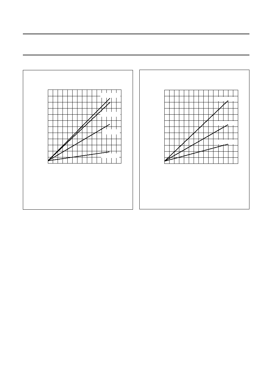
TEST AND APPLICATION INFORMATION
Fig.5
DAC output voltage as a function of
programmed value.
V
CC
= 12 V.
handbook, halfpage
0
00 05
0F
0A
MGH514
4
8
12
14 19 1E 23 28 2D 32 37 3C 3F
data (hex)
VO(DAC)
(V)
VMAX = 12 V
VMAX = 10 V
VMAX = 6 V
VMAX = 1 V
Fig.6
DAC output voltage as a function of
programmed value.
V
MAX
= V
CC
.
handbook, halfpage
0
00 05
0F
0A
MGL533
4
8
12
14 19 1E 23 28 2D 32 37 3C 3F
data (hex)
VO(DAC)
(V)
VCC = 12 V
VCC = 8 V
VCC = 5 V

1999 Apr 29
10
Philips Semiconductors
Product specification
Octuple 6-bit DACs with I
2
C-bus
TDA8444; TDA8444T;
TDA8444AT
PACKAGE OUTLINES
UNIT
A
max.
1
2
b
1
c
E
e
M
H
L
REFERENCES
OUTLINE
VERSION
EUROPEAN
PROJECTION
ISSUE DATE
IEC
JEDEC
EIAJ
mm
inches
DIMENSIONS (inch dimensions are derived from the original mm dimensions)
SOT38-1
92-10-02
95-01-19
A
min.
A
max.
b
max.
w
M
E
e
1
1.40
1.14
0.055
0.045
0.53
0.38
0.32
0.23
21.8
21.4
0.86
0.84
6.48
6.20
0.26
0.24
3.9
3.4
0.15
0.13
0.254
2.54
7.62
0.30
8.25
7.80
0.32
0.31
9.5
8.3
0.37
0.33
2.2
0.087
4.7
0.51
3.7
0.15
0.021
0.015
0.013
0.009
0.01
0.10
0.020
0.19
050G09
MO-001AE
M
H
c
(e )
1
M
E
A
L
seating plane
A
1
w
M
b
1
e
D
A
2
Z
16
1
9
8
b
E
pin 1 index
0
5
10 mm
scale
Note
1. Plastic or metal protrusions of 0.25 mm maximum per side are not included.
(1)
(1)
D
(1)
Z
DIP16: plastic dual in-line package; 16 leads (300 mil); long body
SOT38-1
1999 Apr 29
11
Philips Semiconductors
Product specification
Octuple 6-bit DACs with I
2
C-bus
TDA8444; TDA8444T;
TDA8444AT
UNIT
A
max.
A
1
A
2
A
3
b
p
c
D
(1)
E
(1)
(1)
e
H
E
L
L
p
Q
Z
y
w
v
REFERENCES
OUTLINE
VERSION
EUROPEAN
PROJECTION
ISSUE DATE
IEC
JEDEC
EIAJ
mm
inches
2.65
0.30
0.10
2.45
2.25
0.49
0.36
0.32
0.23
10.5
10.1
7.6
7.4
1.27
10.65
10.00
1.1
1.0
0.9
0.4
8
0
o
o
0.25
0.1
DIMENSIONS (inch dimensions are derived from the original mm dimensions)
Note
1. Plastic or metal protrusions of 0.15 mm maximum per side are not included.
1.1
0.4
SOT162-1
8
16
w
M
b
p
D
detail X
Z
e
9
1
y
0.25
075E03
MS-013AA
pin 1 index
0.10
0.012
0.004
0.096
0.089
0.019
0.014
0.013
0.009
0.41
0.40
0.30
0.29
0.050
1.4
0.055
0.419
0.394
0.043
0.039
0.035
0.016
0.01
0.25
0.01
0.004
0.043
0.016
0.01
X
A
A
1
A
2
H
E
L
p
Q
E
c
L
v
M
A
(A )
3
A
0
5
10 mm
scale
SO16: plastic small outline package; 16 leads; body width 7.5 mm
SOT162-1
95-01-24
97-05-22

1999 Apr 29
12
Philips Semiconductors
Product specification
Octuple 6-bit DACs with I
2
C-bus
TDA8444; TDA8444T;
TDA8444AT
UNIT
A
max.
A
1
A
2
A
3
b
p
c
D
(1)
E
(1)
(1)
e
H
E
L
L
p
Q
Z
y
w
v
REFERENCES
OUTLINE
VERSION
EUROPEAN
PROJECTION
ISSUE DATE
IEC
JEDEC
EIAJ
mm
inches
2.65
0.30
0.10
2.45
2.25
0.49
0.36
0.32
0.23
13.0
12.6
7.6
7.4
1.27
10.65
10.00
1.1
1.0
0.9
0.4
8
0
o
o
0.25
0.1
DIMENSIONS (inch dimensions are derived from the original mm dimensions)
Note
1. Plastic or metal protrusions of 0.15 mm maximum per side are not included.
1.1
0.4
SOT163-1
10
20
w
M
b
p
detail X
Z
e
11
1
D
y
0.25
075E04
MS-013AC
pin 1 index
0.10
0.012
0.004
0.096
0.089
0.019
0.014
0.013
0.009
0.51
0.49
0.30
0.29
0.050
1.4
0.055
0.419
0.394
0.043
0.039
0.035
0.016
0.01
0.25
0.01
0.004
0.043
0.016
0.01
0
5
10 mm
scale
X
A
A
1
A
2
H
E
L
p
Q
E
c
L
v
M
A
(A )
3
A
SO20: plastic small outline package; 20 leads; body width 7.5 mm
SOT163-1
95-01-24
97-05-22

1999 Apr 29
13
Philips Semiconductors
Product specification
Octuple 6-bit DACs with I
2
C-bus
TDA8444; TDA8444T;
TDA8444AT
SOLDERING
Introduction
There is no soldering method that is ideal for all IC
packages. Wave soldering is often preferred when
through-hole and surface mounted components are mixed
on one printed-circuit board. However, wave soldering is
not always suitable for surface mounted ICs, or for
printed-circuits with high population densities. In these
situations reflow soldering is often used.
This text gives a very brief insight to a complex technology.
A more in-depth account of soldering ICs can be found in
our
"Data Handbook IC26; Integrated Circuit Packages"
(order code 9398 652 90011).
DIP
S
OLDERING BY DIPPING OR BY WAVE
The maximum permissible temperature of the solder is
260
∞
C; solder at this temperature must not be in contact
with the joint for more than 5 seconds. The total contact
time of successive solder waves must not exceed
5 seconds.
The device may be mounted up to the seating plane, but
the temperature of the plastic body must not exceed the
specified maximum storage temperature (T
stg max
). If the
printed-circuit board has been pre-heated, forced cooling
may be necessary immediately after soldering to keep the
temperature within the permissible limit.
R
EPAIRING SOLDERED JOINTS
Apply a low voltage soldering iron (less than 24 V) to the
lead(s) of the package, below the seating plane or not
more than 2 mm above it. If the temperature of the
soldering iron bit is less than 300
∞
C it may remain in
contact for up to 10 seconds. If the bit temperature is
between 300 and 400
∞
C, contact may be up to 5 seconds.
SO
R
EFLOW SOLDERING
Reflow soldering techniques are suitable for all SO
packages.
Reflow soldering requires solder paste (a suspension of
fine solder particles, flux and binding agent) to be applied
to the printed-circuit board by screen printing, stencilling or
pressure-syringe dispensing before package placement.
Several techniques exist for reflowing; for example,
thermal conduction by heated belt. Dwell times vary
between 50 and 300 seconds depending on heating
method. Typical reflow temperatures range from
215 to 250
∞
C.
Preheating is necessary to dry the paste and evaporate
the binding agent. Preheating duration: 45 minutes at
45
∞
C.
W
AVE SOLDERING
Wave soldering techniques can be used for all SO
packages if the following conditions are observed:
∑
A double-wave (a turbulent wave with high upward
pressure followed by a smooth laminar wave) soldering
technique should be used.
∑
The longitudinal axis of the package footprint must be
parallel to the solder flow.
∑
The package footprint must incorporate solder thieves at
the downstream end.
During placement and before soldering, the package must
be fixed with a droplet of adhesive. The adhesive can be
applied by screen printing, pin transfer or syringe
dispensing. The package can be soldered after the
adhesive is cured.
Maximum permissible solder temperature is 260
∞
C, and
maximum duration of package immersion in solder is
10 seconds, if cooled to less than 150
∞
C within
6 seconds. Typical dwell time is 4 seconds at 250
∞
C.
A mildly-activated flux will eliminate the need for removal
of corrosive residues in most applications.
R
EPAIRING SOLDERED JOINTS
Fix the component by first soldering two diagonally-
opposite end leads. Use only a low voltage soldering iron
(less than 24 V) applied to the flat part of the lead. Contact
time must be limited to 10 seconds at up to 300
∞
C. When
using a dedicated tool, all other leads can be soldered in
one operation within 2 to 5 seconds between
270 and 320
∞
C.
1999 Apr 29
14
Philips Semiconductors
Product specification
Octuple 6-bit DACs with I
2
C-bus
TDA8444; TDA8444T;
TDA8444AT
DEFINITIONS
LIFE SUPPORT APPLICATIONS
These products are not designed for use in life support appliances, devices, or systems where malfunction of these
products can reasonably be expected to result in personal injury. Philips customers using or selling these products for
use in such applications do so at their own risk and agree to fully indemnify Philips for any damages resulting from such
improper use or sale.
PURCHASE OF PHILIPS I
2
C COMPONENTS
Data sheet status
Objective specification
This data sheet contains target or goal specifications for product development.
Preliminary specification
This data sheet contains preliminary data; supplementary data may be published later.
Product specification
This data sheet contains final product specifications.
Limiting values
Limiting values given are in accordance with the Absolute Maximum Rating System (IEC 134). Stress above one or
more of the limiting values may cause permanent damage to the device. These are stress ratings only and operation
of the device at these or at any other conditions above those given in the Characteristics sections of the specification
is not implied. Exposure to limiting values for extended periods may affect device reliability.
Application information
Where application information is given, it is advisory and does not form part of the specification.
Purchase of Philips I
2
C components conveys a license under the Philips' I
2
C patent to use the
components in the I
2
C system provided the system conforms to the I
2
C specification defined by
Philips. This specification can be ordered using the code 9398 393 40011.

1999 Apr 29
15
Philips Semiconductors
Product specification
Octuple 6-bit DACs with I
2
C-bus
TDA8444; TDA8444T;
TDA8444AT
NOTES

Internet: http://www.semiconductors.philips.com
Philips Semiconductors ≠ a worldwide company
© Philips Electronics N.V. 1999
SCA63
All rights are reserved. Reproduction in whole or in part is prohibited without the prior written consent of the copyright owner.
The information presented in this document does not form part of any quotation or contract, is believed to be accurate and reliable and may be changed
without notice. No liability will be accepted by the publisher for any consequence of its use. Publication thereof does not convey nor imply any license
under patent- or other industrial or intellectual property rights.
Netherlands: Postbus 90050, 5600 PB EINDHOVEN, Bldg. VB,
Tel. +31 40 27 82785, Fax. +31 40 27 88399
New Zealand: 2 Wagener Place, C.P.O. Box 1041, AUCKLAND,
Tel. +64 9 849 4160, Fax. +64 9 849 7811
Norway: Box 1, Manglerud 0612, OSLO,
Tel. +47 22 74 8000, Fax. +47 22 74 8341
Pakistan: see Singapore
Philippines: Philips Semiconductors Philippines Inc.,
106 Valero St. Salcedo Village, P.O. Box 2108 MCC, MAKATI,
Metro MANILA, Tel. +63 2 816 6380, Fax. +63 2 817 3474
Poland: Ul. Lukiska 10, PL 04-123 WARSZAWA,
Tel. +48 22 612 2831, Fax. +48 22 612 2327
Portugal: see Spain
Romania: see Italy
Russia: Philips Russia, Ul. Usatcheva 35A, 119048 MOSCOW,
Tel. +7 095 755 6918, Fax. +7 095 755 6919
Singapore: Lorong 1, Toa Payoh, SINGAPORE 319762,
Tel. +65 350 2538, Fax. +65 251 6500
Slovakia: see Austria
Slovenia: see Italy
South Africa: S.A. PHILIPS Pty Ltd., 195-215 Main Road Martindale,
2092 JOHANNESBURG, P.O. Box 7430 Johannesburg 2000,
Tel. +27 11 470 5911, Fax. +27 11 470 5494
South America: Al. Vicente Pinzon, 173, 6th floor,
04547-130 S√O PAULO, SP, Brazil,
Tel. +55 11 821 2333, Fax. +55 11 821 2382
Spain: Balmes 22, 08007 BARCELONA,
Tel. +34 93 301 6312, Fax. +34 93 301 4107
Sweden: Kottbygatan 7, Akalla, S-16485 STOCKHOLM,
Tel. +46 8 5985 2000, Fax. +46 8 5985 2745
Switzerland: Allmendstrasse 140, CH-8027 ZÐRICH,
Tel. +41 1 488 2741 Fax. +41 1 488 3263
Taiwan: Philips Semiconductors, 6F, No. 96, Chien Kuo N. Rd., Sec. 1,
TAIPEI, Taiwan Tel. +886 2 2134 2886, Fax. +886 2 2134 2874
Thailand: PHILIPS ELECTRONICS (THAILAND) Ltd.,
209/2 Sanpavuth-Bangna Road Prakanong, BANGKOK 10260,
Tel. +66 2 745 4090, Fax. +66 2 398 0793
Turkey: Talatpasa Cad. No. 5, 80640 GÐLTEPE/ISTANBUL,
Tel. +90 212 279 2770, Fax. +90 212 282 6707
Ukraine: PHILIPS UKRAINE, 4 Patrice Lumumba str., Building B, Floor 7,
252042 KIEV, Tel. +380 44 264 2776, Fax. +380 44 268 0461
United Kingdom: Philips Semiconductors Ltd., 276 Bath Road, Hayes,
MIDDLESEX UB3 5BX, Tel. +44 181 730 5000, Fax. +44 181 754 8421
United States: 811 East Arques Avenue, SUNNYVALE, CA 94088-3409,
Tel. +1 800 234 7381, Fax. +1 800 943 0087
Uruguay: see South America
Vietnam: see Singapore
Yugoslavia: PHILIPS, Trg N. Pasica 5/v, 11000 BEOGRAD,
Tel. +381 11 62 5344, Fax.+381 11 63 5777
For all other countries apply to: Philips Semiconductors,
International Marketing & Sales Communications, Building BE-p, P.O. Box 218,
5600 MD EINDHOVEN, The Netherlands, Fax. +31 40 27 24825
Argentina: see South America
Australia: 34 Waterloo Road, NORTH RYDE, NSW 2113,
Tel. +61 2 9805 4455, Fax. +61 2 9805 4466
Austria: Computerstr. 6, A-1101 WIEN, P.O. Box 213,
Tel. +43 1 60 101 1248, Fax. +43 1 60 101 1210
Belarus: Hotel Minsk Business Center, Bld. 3, r. 1211, Volodarski Str. 6,
220050 MINSK, Tel. +375 172 20 0733, Fax. +375 172 20 0773
Belgium: see The Netherlands
Brazil: see South America
Bulgaria: Philips Bulgaria Ltd., Energoproject, 15th floor,
51 James Bourchier Blvd., 1407 SOFIA,
Tel. +359 2 68 9211, Fax. +359 2 68 9102
Canada: PHILIPS SEMICONDUCTORS/COMPONENTS,
Tel. +1 800 234 7381, Fax. +1 800 943 0087
China/Hong Kong: 501 Hong Kong Industrial Technology Centre,
72 Tat Chee Avenue, Kowloon Tong, HONG KONG,
Tel. +852 2319 7888, Fax. +852 2319 7700
Colombia: see South America
Czech Republic: see Austria
Denmark: Sydhavnsgade 23, 1780 COPENHAGEN V,
Tel. +45 33 29 3333, Fax. +45 33 29 3905
Finland: Sinikalliontie 3, FIN-02630 ESPOO,
Tel. +358 9 615 800, Fax. +358 9 6158 0920
France: 51 Rue Carnot, BP317, 92156 SURESNES Cedex,
Tel. +33 1 4099 6161, Fax. +33 1 4099 6427
Germany: Hammerbrookstraþe 69, D-20097 HAMBURG,
Tel. +49 40 2353 60, Fax. +49 40 2353 6300
Hungary: see Austria
India: Philips INDIA Ltd, Band Box Building, 2nd floor,
254-D, Dr. Annie Besant Road, Worli, MUMBAI 400 025,
Tel. +91 22 493 8541, Fax. +91 22 493 0966
Indonesia: PT Philips Development Corporation, Semiconductors Division,
Gedung Philips, Jl. Buncit Raya Kav.99-100, JAKARTA 12510,
Tel. +62 21 794 0040 ext. 2501, Fax. +62 21 794 0080
Ireland: Newstead, Clonskeagh, DUBLIN 14,
Tel. +353 1 7640 000, Fax. +353 1 7640 200
Israel: RAPAC Electronics, 7 Kehilat Saloniki St, PO Box 18053,
TEL AVIV 61180, Tel. +972 3 645 0444, Fax. +972 3 649 1007
Italy: PHILIPS SEMICONDUCTORS, Piazza IV Novembre 3,
20124 MILANO, Tel. +39 2 6752 2531, Fax. +39 2 6752 2557
Japan: Philips Bldg 13-37, Kohnan 2-chome, Minato-ku,
TOKYO 108-8507, Tel. +81 3 3740 5130, Fax. +81 3 3740 5077
Korea: Philips House, 260-199 Itaewon-dong, Yongsan-ku, SEOUL,
Tel. +82 2 709 1412, Fax. +82 2 709 1415
Malaysia: No. 76 Jalan Universiti, 46200 PETALING JAYA, SELANGOR,
Tel. +60 3 750 5214, Fax. +60 3 757 4880
Mexico: 5900 Gateway East, Suite 200, EL PASO, TEXAS 79905,
Tel. +9-5 800 234 7381, Fax +9-5 800 943 0087
Middle East: see Italy
Printed in The Netherlands
545002/750/03/pp16
Date of release: 1999 Apr 29
Document order number:
9397 750 04699