 | –≠–ª–µ–∫—Ç—Ä–æ–Ω–Ω—ã–π –∫–æ–º–ø–æ–Ω–µ–Ω—Ç: TDA8542TS | –°–∫–∞—á–∞—Ç—å:  PDF PDF  ZIP ZIP |

DATA SHEET
Product specification
Supersedes data of 1997 Nov 17
File under Integrated Circuits, IC01
1998 Mar 25
INTEGRATED CIRCUITS
TDA8542TS
2
◊
0.7 W BTL audio amplifier

1998 Mar 25
2
Philips Semiconductors
Product specification
2
◊
0.7 W BTL audio amplifier
TDA8542TS
FEATURES
∑
Flexibility in use
∑
Few external components
∑
Low saturation voltage of output stage
∑
Gain can be fixed with external resistors
∑
Standby mode controlled by CMOS compatible levels
∑
Low standby current
∑
No switch-on/switch-off plops
∑
High supply voltage ripple rejection
∑
Protected against electrostatic discharge
∑
Outputs short-circuit safe to ground, V
CC
and across the
load
∑
Thermally protected.
GENERAL DESCRIPTION
The TDA8542TS is a two channel audio power amplifier
for an output power of 2
◊
0.7 W with a 16
load at a 5 V
supply. At a low supply voltage of 3.3 V an output power of
0.6 W with an 8
load can be obtained. The circuit
contains two Bridge-Tied Load (BTL) amplifiers with a
complementary PNP-NPN output stage and standby/mute
logic. The TDA8542TS is available in a SSOP20 package.
APPLICATIONS
∑
Portable consumer products
∑
Personal computers
∑
Motor-driver (servo).
QUICK REFERENCE DATA
ORDERING INFORMATION
SYMBOL
PARAMETER
CONDITIONS
MIN.
TYP.
MAX.
UNIT
V
CC
supply voltage
2.2
5
18
V
I
q
quiescent current
V
CC
= 5 V
-
15
22
mA
I
stb
standby current
-
-
10
µ
A
P
o
output power
THD = 10%; R
L
= 8
; V
CC
= 3.3 V 0.45
0.55
-
W
THD = 10%; R
L
= 16
; V
CC
= 5 V
0.6
0.7
-
W
THD
total harmonic distortion
P
o
= 0.4 W
-
0.15
-
%
SVRR
supply voltage ripple rejection
50
-
-
dB
TYPE
NUMBER
PACKAGE
NAME
DESCRIPTION
VERSION
TDA8542TS
SSOP20
plastic shrink small outline package; 20 leads; body width 4.4 mm
SOT266-1

1998 Mar 25
3
Philips Semiconductors
Product specification
2
◊
0.7 W BTL audio amplifier
TDA8542TS
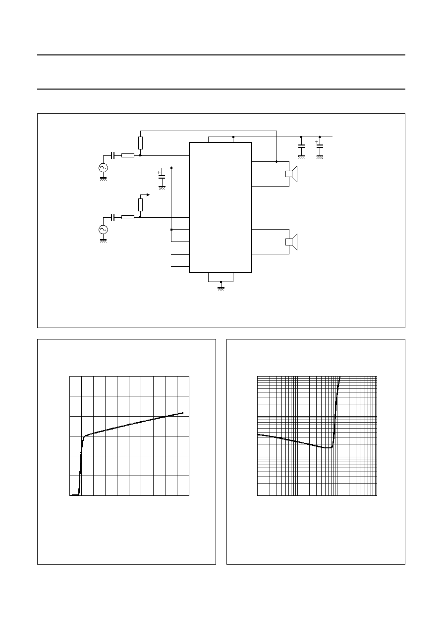
BLOCK DIAGRAM
Fig.1 Block diagram.
handbook, full pagewidth
MBK445
STANDBY/MUTE LOGIC
R
R
20 k
20 k
INL
-
INL
+
VCCL
OUTL
-
OUTL
+
-
-
+
-
-
+
STANDBY/MUTE LOGIC
R
R
20 k
20 k
INR
-
INR
+
VCCR
SVR
MODE
OUTR
-
OUTR
+
-
-
+
-
-
+
BTL/SE
LGND
RGND
VCCL VCCR
20
11
18
3
13
8
1
10
17
16
14
n.c.
2
n.c.
7
n.c.
9
n.c.
12
n.c.
19
15
5
4
6
TDA8542TS

1998 Mar 25
4
Philips Semiconductors
Product specification
2
◊
0.7 W BTL audio amplifier
TDA8542TS
PINNING
SYMBOL
PIN
DESCRIPTION
LGND
1
ground, left channel
n.c.
2
not connected
OUTL+
3
positive loudspeaker terminal,
left channel
MODE
4
operating mode select (standby,
mute, operating)
SVR
5
half supply voltage, decoupling
ripple rejection
BTL/SE
6
BTL loudspeaker or SE
headphone operation
n.c.
7
not connected
OUTR+
8
positive loudspeaker terminal,
right channel
n.c.
9
not connected
RGND
10
ground, right channel
V
CCR
11
supply voltage, right channel
n.c.
12
not connected
OUTR
-
13
negative loudspeaker terminal,
right channel
INR
-
14
negative input, right channel
INR+
15
positive input, right channel
INL+
16
positive input, left channel
INL
-
17
negative input, left channel
OUTL
-
18
negative loudspeaker terminal,
left channel
n.c.
19
not connected
V
CCL
20
supply voltage, left channel
Fig.2 Pin configuration.
handbook, halfpage
TDA8542TS
MBK453
1
2
3
4
5
6
7
8
9
10
20
19
18
17
16
15
14
13
12
11
LGND
n.c.
OUTL
+
MODE
SVR
BTL/SE
n.c.
OUTR
+
n.c.
RGND
VCCL
n.c.
OUTL
-
INL
-
INL
+
INR
+
INR
-
OUTR
-
n.c.
VCCR
FUNCTIONAL DESCRIPTION
The TDA8542TS is a 2
◊
0.7 W BTL audio power amplifier
capable of delivering 2
◊
0.7 W output power to a 16
load at THD = 10% using a 5 V power supply. Using the
MODE pin the device can be switched to standby and
mute condition. The device is protected by an internal
thermal shutdown protection mechanism. The gain can be
set within a range from 6 to 30 dB by external feedback
resistors.
Power amplifier
The power amplifier is a Bridge-Tied Load (BTL) amplifier
with a complementary PNP-NPN output stage.
The voltage loss on the positive supply line is the
saturation voltage of a PNP power transistor, on the
negative side the saturation voltage of a NPN power
transistor. The total voltage loss is <1 V and with a 5 V
supply voltage and with a 16
loudspeaker an output
power of 0.7 W can be delivered.
Mode select pin
The device is in the standby mode (with a very low current
consumption) if the voltage at the MODE pin is
>(V
CC
-
0.5 V), or if this pin is floating. At a MODE voltage
level of less than 0.5 V the amplifier is fully operational.
In the range between 1.5 V and V
CC
-
1.5 V the amplifier
is in mute condition. The mute condition is useful to
suppress plop noise at the output caused by charging of
the input capacitor.

1998 Mar 25
5
Philips Semiconductors
Product specification
2
◊
0.7 W BTL audio amplifier
TDA8542TS
Headphone connection
A headphone can be connected to the amplifier using two
coupling capacitors for each channel. The common
GND pin of the headphone is connected to the ground of
the amplifier (see Fig.13). In this case the BTL/SE pin must
be either at a logic HIGH level or not connected at all.
The two coupling capacitors can be omitted if it is allowed
to connect the common GND pin of the headphone jack
not to ground, but to a voltage level of
1
/
2
V
CC
. See Fig.4 for
the application diagram. In this case the BTL/SE pin must
be either at a logic LOW level or connected to ground.
If the BTL/SE pin is at a LOW level, the power amplifier for
the positive loudspeaker terminal is always in mute
condition.
LIMITING VALUES
In accordance with the Absolute Maximum Rating System (IEC 134).
QUALITY SPECIFICATION
In accordance with
"SNW-FQ-611-E".
THERMAL CHARACTERISTICS
Note
1. See Section "Thermal design considerations".
Table 1
Maximum ambient temperature at different conditions
Note
1. See Section "Thermal design considerations".
SYMBOL
PARAMETER
CONDITIONS
MIN.
MAX.
UNIT
V
CC
supply voltage
operating
-
0.3
+18
V
V
I
input voltage
-
0.3
V
CC
+ 0.3
V
I
ORM
repetitive peak output current
-
1
A
T
stg
storage temperature
non-operating
-
55
+150
∞
C
T
amb
operating ambient temperature
-
40
+85
∞
C
V
sc
AC and DC short-circuit safe voltage
-
10
V
P
tot
total power dissipation
-
1.12
W
SYMBOL
PARAMETER
CONDITIONS
VALUE
UNIT
R
th(j-a)
thermal resistance from junction to ambient
in free air
110
(1)
K/W
V
CC
(V)
R
L
(
)
P
o
(W)
CONTINUOUS SINE WAVE DRIVEN
P
max
(W)
T
amb(max)
(
∞
C)
3.3
4
2
◊
0.65
1.12
27
(1)
3.3
8
2
◊
0.55
0.60
84
5
8
2
◊
1.2
1.33
-
(1)
5
16
2
◊
0.70
0.80
62

1998 Mar 25
6
Philips Semiconductors
Product specification
2
◊
0.7 W BTL audio amplifier
TDA8542TS
DC CHARACTERISTICS
V
CC
= 5 V; T
amb
= 25
∞
C; R
L
= 8
; V
MODE
= 0 V; measured in test circuit Fig.3; unless otherwise specified.
Notes
1. With a load connected at the outputs the quiescent current will increase, the maximum of this increase being equal
to the DC output offset voltage divided by R
L
.
2. The DC output voltage with respect to ground is approximately
1
/
2
V
CC
.
SYMBOL
PARAMETER
CONDITIONS
MIN.
TYP.
MAX.
UNIT
V
CC
supply voltage
operating
2.2
5
18
V
I
q
quiescent current
R
L
=
; note 1
-
15
22
mA
I
stb
standby current
V
MODE
= V
CC
-
-
10
µ
A
V
O
DC output voltage
note 2
-
2.2
-
V
V
OUT+
-
V
OUT
-
differential output voltage offset
-
-
50
mV
I
IN+
, I
IN
-
input bias current
-
-
500
nA
V
MODE
input voltage mode select
operating
0
-
0.5
V
mute
1.5
-
V
CC
-
1.5 V
standby
V
CC
-
0.5
-
V
CC
V
I
MODE
input current mode select
0 < V
MODE
< V
CC
-
-
20
µ
A
V
BTL/SE
input voltage BTL/SE pin
single-ended
0
-
0.6
V
BTL
2
-
V
CC
V
I
BTL/SE
input current BTL/SE pin
V
BTL/SE
= 0
-
-
100
µ
A

1998 Mar 25
7
Philips Semiconductors
Product specification
2
◊
0.7 W BTL audio amplifier
TDA8542TS
AC CHARACTERISTICS
V
CC
= 5 V; T
amb
= 25
∞
C; R
L
= 8
; f = 1 kHz; V
MODE
= 0 V; measured in test circuit Fig.3; unless otherwise specified.
Notes
1. Gain of the amplifier is
in test circuit of Fig.3.
2. The noise output voltage is measured at the output in a frequency range from 20 Hz to 20 kHz (unweighted), with a
source impedance of R
S
= 0
at the input.
3. Supply voltage ripple rejection is measured at the output, with a source impedance of R
S
= 0
at the input.
The ripple voltage is a sine wave with a frequency of 1 kHz and an amplitude of 100 mV (RMS), which is applied to
the positive supply rail.
4. Supply voltage ripple rejection is measured at the output, with a source impedance of R
S
= 0
at the input.
The ripple voltage is a sine wave with a frequency between 100 Hz and 20 kHz and an amplitude of 100 mV (RMS),
which is applied to the positive supply rail.
5. Output voltage in mute position is measured with a 1 V (RMS) input voltage in a bandwidth of 20 kHz, so including
noise.
SYMBOL
PARAMETER
CONDITIONS
MIN.
TYP.
MAX.
UNIT
P
o
output power
at V
CC
= 5 V
THD = 10%; R
L
= 8
-
1.2
-
W
THD = 10%; R
L
= 16
-
0.70
-
W
THD = 0.5%; R
L
= 8
-
0.9
-
W
THD = 0.5%; R
L
= 16
-
0.5
-
W
at V
CC
= 3.3 V
THD = 10%; R
L
= 4
-
0.65
-
W
THD = 10%; R
L
= 8
-
0.55
-
W
THD = 0.5%; R
L
= 4
-
0.45
-
W
THD = 0.5%; R
L
= 8
-
0.38
-
W
THD
total harmonic distortion
P
o
= 0.4 W
-
0.15
0.3
%
G
v(cl)
closed-loop voltage gain
note 1
6
-
30
dB
Z
i(dif)
differential input impedance
-
100
-
k
V
n(o)
noise output voltage
note 2
-
-
100
µ
V
SVRR
supply voltage ripple rejection
note 3
50
-
-
dB
note 4
40
-
-
dB
V
o(mute)
output voltage in mute condition
note 5
-
-
200
µ
V
cs
channel separation
40
-
-
dB
2
R2
R1
-------
◊

1998 Mar 25
8
Philips Semiconductors
Product specification
2
◊
0.7 W BTL audio amplifier
TDA8542TS
TEST AND APPLICATION INFORMATION
Test conditions
Because the application can be either Bridge-Tied Load
(BTL) or Single-Ended (SE), the curves of each application
are shown separately.
The thermal resistance = 110 K/W for the SSOP20; the
maximum sine wave power dissipation for T
amb
= 25
∞
C is:
For T
amb
= 60
∞
C the maximum total power dissipation is:
Thermal design considerations
The `measured' thermal resistance of the IC package is
highly dependent on the configuration and size of the
application board. Data may not be comparable between
different semiconductor manufacturers because the
application boards and test methods are not (yet)
standardized. Also, the thermal performance of packages
for a specific application may be different than presented
here, because the configuration of the application boards
(copper area) may be different. Philips Semiconductors
uses FR-4 type application boards with 1 oz copper traces
with solder coating.
The SSOP package has improved thermal conductivity
which reduces the thermal resistance. Using a practical
PCB layout (see Fig.22) with wider copper tracks to the
corner pins and just under the IC, the thermal resistance
from junction to ambient can be reduced to approximately
80 K/W. For T
amb
= 60
∞
C the maximum total power
dissipation for this PCB layout is:
BTL application
T
amb
= 25
∞
C if not specially mentioned, V
CC
= 5 V,
f = 1 kHz, R
L
= 8
, G
v
= 20 dB, audio band-pass
22 Hz to 22 kHz.
The BTL application diagram is illustrated in Fig.3.
The quiescent current has been measured without any
load impedance. The total harmonic distortion as a
150
25
≠
110
----------------------
1.14 W
=
150
60
≠
110
----------------------
0.82 W
=
150
60
≠
80
----------------------
1.12 W
=
function of frequency was measured with a low-pass filter
of 80 kHz. The value of capacitor C3 influences the
behaviour of the SVRR at low frequencies, increasing the
value of C3 increases the performance of the SVRR.
The figure of the mode select voltage (V
ms
) as a function
of the supply voltage shows three areas; operating, mute
and standby. It shows, that the DC-switching levels of the
mute and standby respectively depends on the supply
voltage level.
SE application
T
amb
= 25
∞
C if not specially mentioned, V
CC
= 7.5 V,
f = 1 kHz, R
L
= 4
, G
v
= 20 dB, audio band-pass
22 Hz to 22 kHz.
The SE application diagram is illustrated in Fig.14.
If the BTL/SE pin (pin 6) is connected to ground, the
positive outputs (pins 3 and 8) will be in mute condition
with a DC level of
1
/
2
V
CC
. When a headphone is used
(R
L
25
) the SE headphone application can be used
without output coupling capacitors; load between negative
output and one of the positive outputs (e.g. pin 3) as
common pin. The channel separation will be less in
comparison with the application using a coupling capacitor
connected to ground.
Increasing the value of electrolytic capacitor C3 will result
in a better channel separation. Because the positive output
is not designed for high output current (2
◊
I
o
) at low load
impedance (
16
), the SE application with output
capacitors connected to ground is advised. The capacitor
value of C4/C5 in combination with the load impedance
determines the low frequency behaviour. The THD as a
function of frequency was measured using a low-pass filter
of 80 kHz. The value of capacitor C3 influences the
behaviour of the SVRR at low frequencies, increasing the
value of C3 increases the performance of the SVRR.
General remark
The frequency characteristic can be adapted by
connecting a small capacitor across the feedback resistor.
To improve the immunity of HF radiation in radio circuit
applications, a small capacitor can be connected in
parallel with the feedback resistor (56 k
); this creates a
low-pass filter.
1998 Mar 25
9
Philips Semiconductors
Product specification
2
◊
0.7 W BTL audio amplifier
TDA8542TS
BTL APPLICATION
handbook, full pagewidth
MBK443
17
VCC
ViL
OUTL
-
INL
-
INL
+
OUTL
+
18
100 nF
100
µ
F
20
11
1
10
TDA8542TS
16
OUTR
-
GND
RL
INR
-
14
INR
+
SVR
15
5
4
6
MODE
BTL/SE
3
OUTR
-
OUTR
+
13
RL
8
C3
47
µ
F
1
µ
F
1
µ
F
R1
R2
R4
10 k
10 k
50 k
50 k
R3
ViR
Fig.3 BTL application.
Pins 2, 7, 9, 12 and 19 are not connected.
Gain left
2
R2
R1
--------
◊
=
Gain right
2
R4
R3
--------
◊
=
Fig.4 I
q
as a function of V
CC
.
R
L
=
.
handbook, halfpage
0
Iq
(mA)
VCC (V)
20
30
10
0
4
20
8
12
16
MGD890
Fig.5 THD as a function of P
o
.
f = 1 kHz; G
v
= 20 dB; V
CC
= 5 V; R
L
= 8
.
handbook, halfpage
10
1
THD
(%)
10
-
2
10
-
1
MBK446
10
-
2
10
-
1
1
Po (W)
10
1998 Mar 25
10
Philips Semiconductors
Product specification
2
◊
0.7 W BTL audio amplifier
TDA8542TS
Fig.6 THD as a function of frequency.
P
o
= 0.5 W; G
v
= 20 dB; V
CC
= 5 V; R
L
= 8
.
handbook, halfpage
10
1
10
-
1
10
-
2
MBK447
10
10
2
10
3
10
4
THD
(%)
f (Hz)
10
5
Fig.7
Channel separation as a function of
frequency.
V
CC
= 5 V, V
o
= 2 V, R
L
= 8
.
(1) G
v
= 30 dB.
(2) G
v
= 20 dB.
(3) G
v
= 6 dB.
handbook, halfpage
-
100
-
90
-
80
-
70
-
60
MGD893
10
10
2
10
3
10
4
10
5
f (Hz)
cs
(dB)
(1)
(2)
(3)
Fig.8 SVRR as a function of frequency.
V
CC
= 5 V, R
s
= 0
, V
r
= 100 mV.
(1) G
v
= 30 dB.
(2) G
v
= 20 dB.
(3) G
v
= 6 dB.
handbook, halfpage
-
80
-
60
-
40
-
20
MGD894
10
2
10
10
3
SVRR
(dB)
f (Hz)
10
4
10
5
(1)
(2)
(3)
Fig.9 P
o
as a function of V
CC
.
THD = 10%.
(1) R
L
= 8
.
(2) R
L
= 16
.
handbook, halfpage
0
4
8
Po
(W)
VCC (V)
12
2.5
0
2
1.5
1
0.5
MBK448
(1)
(2)

1998 Mar 25
11
Philips Semiconductors
Product specification
2
◊
0.7 W BTL audio amplifier
TDA8542TS
Fig.10 Worst case power dissipation as a function
of V
CC
.
(1) R
L
= 8
.
(2) R
L
= 16
.
handbook, halfpage
0
3
(1)
(2)
2
VCC (V)
1
0
4
8
12
MBK449
P
(W)
Fig.11 P as a function of P
o
.
Sine wave of 1 kHz; V
CC
= 5 V; R
L
= 8
.
handbook, halfpage
0
3
2
1
0
0.5
2.5
1
1.5
2
Po (W)
MBK450
P
(W)
Fig.12 V
o
as a function of V
ms
.
Band-pass = 22 Hz to 22 kHz.
(1) V
CC
= 3 V.
(2) V
CC
= 5 V.
(3) V
CC
= 12 V.
handbook, halfpage
1
10
10
-
2
10
-
1
10
-
3
10
-
4
10
-
6
10
-
5
MGD898
10
-
1
1
Vo
(V)
Vms (V)
10
10
2
(1)
(2)
(3)
Fig.13 V
MODE
as a function of V
P
.
handbook, halfpage
0
4
8
VMODE
(V)
16
16
12
4
0
8
12
VP (V)
MGL210
operating
mute
standby

1998 Mar 25
12
Philips Semiconductors
Product specification
2
◊
0.7 W BTL audio amplifier
TDA8542TS
SE APPLICATION
handbook, full pagewidth
MBK444
17
VCC
ViL
OUTL
-
INL
-
INL
+
OUTL
+
18
100 nF
470
µ
F
C4
470
µ
F
C5
100
µ
F
20
11
1
10
TDA8542TS
16
OUTR
-
GND
RL = 8
RL = 8
INR
-
14
INR
+
SVR
15
5
4
6
MODE
BTL/SE
3
OUTR
-
OUTR
+
13
8
C3
47
µ
F
1
µ
F
1
µ
F
R1
R2
R4
10 k
10 k
100 k
100 k
R3
ViR
Fig.14 Single-ended application.
Pins 2, 7, 9, 12 and 19 are not connected.
Gain left
R2
R1
--------
=
Gain right
R4
R3
--------
=
Fig.15 THD as a function of P
o
.
f = 1 kHz, G
v
= 20 dB.
(1) V
CC
= 7.5 V, R
L
= 4
.
(2) V
CC
= 9 V, R
L
= 8
.
(3) V
CC
= 12 V, R
L
= 16
.
handbook, halfpage
10
1
Po (W)
THD
(%)
10
-
1
10
-
2
MGD899
10
-
2
10
-
1
1
(1)
(2)
10
(3)
Fig.16 THD as a function of frequency.
P
o
= 0.5 W, G
v
= 20 dB.
(1) V
CC
= 7.5 V, R
L
= 4
.
(2) V
CC
= 9 V, R
L
= 8
.
(3) V
CC
= 12 V, R
L
= 16
.
handbook, halfpage
10
1
THD
(%)
f (Hz)
10
-
1
10
-
2
MGD900
10
10
2
10
3
10
4
10
5
(1)
(2)
(3)
1998 Mar 25
13
Philips Semiconductors
Product specification
2
◊
0.7 W BTL audio amplifier
TDA8542TS
Fig.17 Channel separation as a function of
frequency.
V
o
= 1 V, G
v
= 20 dB.
(1) V
CC
= 5 V, R
L
= 32
, to buffer.
(2) V
CC
= 7.5 V, R
L
= 4
.
(3) V
CC
= 9 V, R
L
= 8
.
(4) V
CC
= 12 V, R
L
= 16
.
(5) V
CC
= 5 V, R
L
= 32
.
handbook, halfpage
-
100
-
80
-
60
-
40
-
20
MGD901
10
(2)
10
2
10
3
10
4
f (Hz)
10
5
(4)
(5)
(1)
(3)
cs
(dB)
Fig.18 SVRR as a function of frequency.
R
S
= 0
, V
ripple
= 100 mV.
(1) G
v
= 24 dB.
(2) G
v
= 20 dB.
(3) G
v
= 0 dB.
handbook, halfpage
-
80
-
60
-
40
-
20
MGD902
10
10
2
10
3
SVRR
(dB)
f (Hz)
10
4
10
5
(1)
(2)
(3)
Fig.19 P
o
as a function of V
CC
.
THD = 10%.
(1) R
L
= 4
.
(2) R
L
= 8
.
(3) R
L
= 16
.
handbook, halfpage
0
(1)
(2)
(3)
4
8
Po
(W)
VCC (V)
16
2
0
1.6
12
1.2
0.8
0.4
MBK451
Fig.20 Worst case power dissipation as a function
of V
CC
.
THD = 10%.
(1) R
L
= 4
.
(2) R
L
= 8
.
(3) R
L
= 16
.
handbook, halfpage
0
3
2
VCC (V)
1
0
4
8
(1)
(2)
(3)
16
12
MBK452
P
(W)

1998 Mar 25
14
Philips Semiconductors
Product specification
2
◊
0.7 W BTL audio amplifier
TDA8542TS
Fig.21 P as a function of P
o
.
f = 1 kHz.
(1) V
CC
= 12 V, R
L
= 16
.
(2) V
CC
= 7.5 V, R
L
= 4
.
(3) V
CC
= 9 V, R
L
= 8
.
handbook, halfpage
0
(1)
(2)
(3)
2.4
1.6
0.8
0
0.4
0.8
1.6
1.2
P
(W)
Po (W)
MGD905

1998 Mar 25
15
Philips Semiconductors
Product specification
2
◊
0.7 W BTL audio amplifier
TDA8542TS
Fig.22 Printed-circuit board layout (BTL).
handbook, full pagewidth
-
OUT1
+
OUT1
-
OUT2
+
OUT2
+
VCC
IN1
IN2
CIC
Nijmegen
MODE
1
20
11
10
GND
TDA
8542TS
8547TS
SELECT
11 k
10 k
10 k
11 k
56 k
56 k
1
µ
F
1
µ
F
47
µ
F
100
µ
F
100 nF
TDA
8542/47TS
MGK997
b. Top view components layout.
a. Top view copper layout.
1998 Mar 25
16
Philips Semiconductors
Product specification
2
◊
0.7 W BTL audio amplifier
TDA8542TS
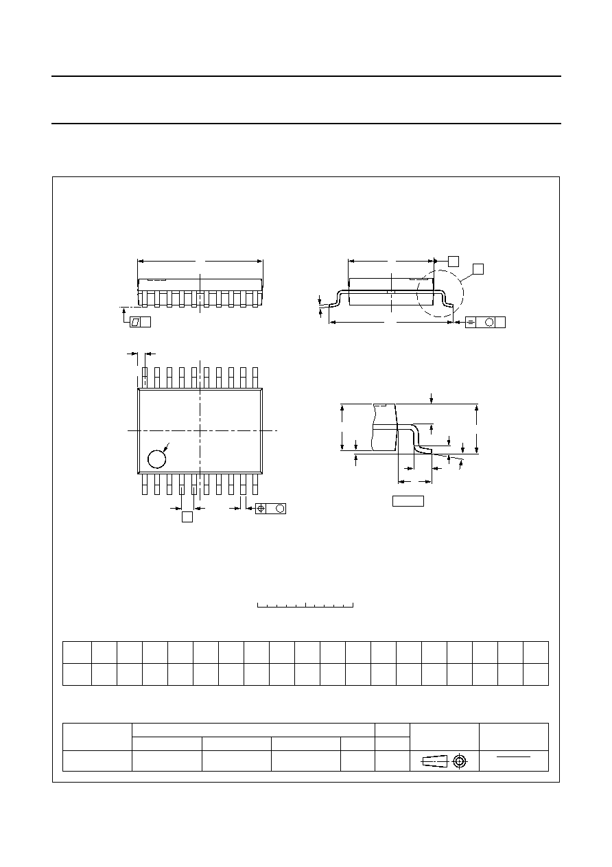
PACKAGE OUTLINE
UNIT
A
1
A
2
A
3
b
p
c
D
(1)
E
(1)
(1)
e
H
E
L
L
p
Q
Z
y
w
v
REFERENCES
OUTLINE
VERSION
EUROPEAN
PROJECTION
ISSUE DATE
IEC
JEDEC
EIAJ
mm
0.15
0
1.4
1.2
0.32
0.20
0.20
0.13
6.6
6.4
4.5
4.3
0.65
1.0
0.2
6.6
6.2
0.65
0.45
0.48
0.18
10
0
o
o
0.13
0.1
DIMENSIONS (mm are the original dimensions)
Note
1. Plastic or metal protrusions of 0.20 mm maximum per side are not included.
0.75
0.45
SOT266-1
90-04-05
95-02-25
w
M
A
A
1
A
2
b
p
D
H
E
L
p
Q
detail X
E
Z
e
c
L
v
M
A
X
(A )
3
A
y
0.25
1
10
20
11
pin 1 index
0
2.5
5 mm
scale
SSOP20: plastic shrink small outline package; 20 leads; body width 4.4 mm
SOT266-1
A
max.
1.5

1998 Mar 25
17
Philips Semiconductors
Product specification
2
◊
0.7 W BTL audio amplifier
TDA8542TS
SOLDERING
Introduction
There is no soldering method that is ideal for all IC
packages. Wave soldering is often preferred when
through-hole and surface mounted components are mixed
on one printed-circuit board. However, wave soldering is
not always suitable for surface mounted ICs, or for
printed-circuits with high population densities. In these
situations reflow soldering is often used.
This text gives a very brief insight to a complex technology.
A more in-depth account of soldering ICs can be found in
our
"IC Package Databook" (order code 9398 652 90011).
Reflow soldering
Reflow soldering techniques are suitable for all SSOP
packages.
Reflow soldering requires solder paste (a suspension of
fine solder particles, flux and binding agent) to be applied
to the printed-circuit board by screen printing, stencilling or
pressure-syringe dispensing before package placement.
Several techniques exist for reflowing; for example,
thermal conduction by heated belt. Dwell times vary
between 50 and 300 seconds depending on heating
method. Typical reflow temperatures range from
215 to 250
∞
C.
Preheating is necessary to dry the paste and evaporate
the binding agent. Preheating duration: 45 minutes at
45
∞
C.
Wave soldering
Wave soldering is not recommended for SSOP packages.
This is because of the likelihood of solder bridging due to
closely-spaced leads and the possibility of incomplete
solder penetration in multi-lead devices.
If wave soldering cannot be avoided, the following
conditions must be observed:
∑
A double-wave (a turbulent wave with high upward
pressure followed by a smooth laminar wave)
soldering technique should be used.
∑
The longitudinal axis of the package footprint must
be parallel to the solder flow and must incorporate
solder thieves at the downstream end.
Even with these conditions, only consider wave
soldering SSOP packages that have a body width of
4.4 mm, that is SSOP16 (SOT369-1) or
SSOP20 (SOT266-1).
During placement and before soldering, the package must
be fixed with a droplet of adhesive. The adhesive can be
applied by screen printing, pin transfer or syringe
dispensing. The package can be soldered after the
adhesive is cured.
Maximum permissible solder temperature is 260
∞
C, and
maximum duration of package immersion in solder is
10 seconds, if cooled to less than 150
∞
C within
6 seconds. Typical dwell time is 4 seconds at 250
∞
C.
A mildly-activated flux will eliminate the need for removal
of corrosive residues in most applications.
Repairing soldered joints
Fix the component by first soldering two diagonally-
opposite end leads. Use only a low voltage soldering iron
(less than 24 V) applied to the flat part of the lead. Contact
time must be limited to 10 seconds at up to 300
∞
C. When
using a dedicated tool, all other leads can be soldered in
one operation within 2 to 5 seconds between
270 and 320
∞
C.

1998 Mar 25
18
Philips Semiconductors
Product specification
2
◊
0.7 W BTL audio amplifier
TDA8542TS
DEFINITIONS
LIFE SUPPORT APPLICATIONS
These products are not designed for use in life support appliances, devices, or systems where malfunction of these
products can reasonably be expected to result in personal injury. Philips customers using or selling these products for
use in such applications do so at their own risk and agree to fully indemnify Philips for any damages resulting from such
improper use or sale.8
Data sheet status
Objective specification
This data sheet contains target or goal specifications for product development.
Preliminary specification
This data sheet contains preliminary data; supplementary data may be published later.
Product specification
This data sheet contains final product specifications.
Limiting values
Limiting values given are in accordance with the Absolute Maximum Rating System (IEC 134). Stress above one or
more of the limiting values may cause permanent damage to the device. These are stress ratings only and operation
of the device at these or at any other conditions above those given in the Characteristics sections of the specification
is not implied. Exposure to limiting values for extended periods may affect device reliability.
Application information
Where application information is given, it is advisory and does not form part of the specification.

1998 Mar 25
19
Philips Semiconductors
Product specification
2
◊
0.7 W BTL audio amplifier
TDA8542TS
NOTES

Internet: http://www.semiconductors.philips.com
Philips Semiconductors ≠ a worldwide company
© Philips Electronics N.V. 1997
SCA56
All rights are reserved. Reproduction in whole or in part is prohibited without the prior written consent of the copyright owner.
The information presented in this document does not form part of any quotation or contract, is believed to be accurate and reliable and may be changed
without notice. No liability will be accepted by the publisher for any consequence of its use. Publication thereof does not convey nor imply any license
under patent- or other industrial or intellectual property rights.
Netherlands: Postbus 90050, 5600 PB EINDHOVEN, Bldg. VB,
Tel. +31 40 27 82785, Fax. +31 40 27 88399
New Zealand: 2 Wagener Place, C.P.O. Box 1041, AUCKLAND,
Tel. +64 9 849 4160, Fax. +64 9 849 7811
Norway: Box 1, Manglerud 0612, OSLO,
Tel. +47 22 74 8000, Fax. +47 22 74 8341
Philippines: Philips Semiconductors Philippines Inc.,
106 Valero St. Salcedo Village, P.O. Box 2108 MCC, MAKATI,
Metro MANILA, Tel. +63 2 816 6380, Fax. +63 2 817 3474
Poland: Ul. Lukiska 10, PL 04-123 WARSZAWA,
Tel. +48 22 612 2831, Fax. +48 22 612 2327
Portugal: see Spain
Romania: see Italy
Russia: Philips Russia, Ul. Usatcheva 35A, 119048 MOSCOW,
Tel. +7 095 755 6918, Fax. +7 095 755 6919
Singapore: Lorong 1, Toa Payoh, SINGAPORE 1231,
Tel. +65 350 2538, Fax. +65 251 6500
Slovakia: see Austria
Slovenia: see Italy
South Africa: S.A. PHILIPS Pty Ltd., 195-215 Main Road Martindale,
2092 JOHANNESBURG, P.O. Box 7430 Johannesburg 2000,
Tel. +27 11 470 5911, Fax. +27 11 470 5494
South America: Al. Vicente Pinzon, 173, 6th floor,
04547-130 S√O PAULO, SP, Brazil,
Tel. +55 11 821 2333, Fax. +55 11 821 2382
Spain: Balmes 22, 08007 BARCELONA,
Tel. +34 3 301 6312, Fax. +34 3 301 4107
Sweden: Kottbygatan 7, Akalla, S-16485 STOCKHOLM,
Tel. +46 8 632 2000, Fax. +46 8 632 2745
Switzerland: Allmendstrasse 140, CH-8027 ZÐRICH,
Tel. +41 1 488 2686, Fax. +41 1 481 7730
Taiwan: Philips Semiconductors, 6F, No. 96, Chien Kuo N. Rd., Sec. 1,
TAIPEI, Taiwan Tel. +886 2 2134 2865, Fax. +886 2 2134 2874
Thailand: PHILIPS ELECTRONICS (THAILAND) Ltd.,
209/2 Sanpavuth-Bangna Road Prakanong, BANGKOK 10260,
Tel. +66 2 745 4090, Fax. +66 2 398 0793
Turkey: Talatpasa Cad. No. 5, 80640 GÐLTEPE/ISTANBUL,
Tel. +90 212 279 2770, Fax. +90 212 282 6707
Ukraine: PHILIPS UKRAINE, 4 Patrice Lumumba str., Building B, Floor 7,
252042 KIEV, Tel. +380 44 264 2776, Fax. +380 44 268 0461
United Kingdom: Philips Semiconductors Ltd., 276 Bath Road, Hayes,
MIDDLESEX UB3 5BX, Tel. +44 181 730 5000, Fax. +44 181 754 8421
United States: 811 East Arques Avenue, SUNNYVALE, CA 94088-3409,
Tel. +1 800 234 7381
Uruguay: see South America
Vietnam: see Singapore
Yugoslavia: PHILIPS, Trg N. Pasica 5/v, 11000 BEOGRAD,
Tel. +381 11 625 344, Fax.+381 11 635 777
For all other countries apply to: Philips Semiconductors,
International Marketing & Sales Communications, Building BE-p,
P.O. Box 218, 5600 MD EINDHOVEN, The Netherlands, Fax. +31 40 27 24825
Argentina: see South America
Australia: 34 Waterloo Road, NORTH RYDE, NSW 2113,
Tel. +61 2 9805 4455, Fax. +61 2 9805 4466
Austria: Computerstr. 6, A-1101 WIEN, P.O. Box 213, Tel. +43 160 1010,
Fax. +43 160 101 1210
Belarus: Hotel Minsk Business Center, Bld. 3, r. 1211, Volodarski Str. 6,
220050 MINSK, Tel. +375 172 200 733, Fax. +375 172 200 773
Belgium: see The Netherlands
Brazil: see South America
Bulgaria: Philips Bulgaria Ltd., Energoproject, 15th floor,
51 James Bourchier Blvd., 1407 SOFIA,
Tel. +359 2 689 211, Fax. +359 2 689 102
Canada: PHILIPS SEMICONDUCTORS/COMPONENTS,
Tel. +1 800 234 7381
China/Hong Kong: 501 Hong Kong Industrial Technology Centre,
72 Tat Chee Avenue, Kowloon Tong, HONG KONG,
Tel. +852 2319 7888, Fax. +852 2319 7700
Colombia: see South America
Czech Republic: see Austria
Denmark: Prags Boulevard 80, PB 1919, DK-2300 COPENHAGEN S,
Tel. +45 32 88 2636, Fax. +45 31 57 0044
Finland: Sinikalliontie 3, FIN-02630 ESPOO,
Tel. +358 9 615800, Fax. +358 9 61580920
France: 51 Rue Carnot, BP317, 92156 SURESNES Cedex,
Tel. +33 1 40 99 6161, Fax. +33 1 40 99 6427
Germany: Hammerbrookstraþe 69, D-20097 HAMBURG,
Tel. +49 40 23 53 60, Fax. +49 40 23 536 300
Greece: No. 15, 25th March Street, GR 17778 TAVROS/ATHENS,
Tel. +30 1 4894 339/239, Fax. +30 1 4814 240
Hungary: see Austria
India: Philips INDIA Ltd, Band Box Building, 2nd floor,
254-D, Dr. Annie Besant Road, Worli, MUMBAI 400 025,
Tel. +91 22 493 8541, Fax. +91 22 493 0966
Indonesia: see Singapore
Ireland: Newstead, Clonskeagh, DUBLIN 14,
Tel. +353 1 7640 000, Fax. +353 1 7640 200
Israel: RAPAC Electronics, 7 Kehilat Saloniki St, PO Box 18053,
TEL AVIV 61180, Tel. +972 3 645 0444, Fax. +972 3 649 1007
Italy: PHILIPS SEMICONDUCTORS, Piazza IV Novembre 3,
20124 MILANO, Tel. +39 2 6752 2531, Fax. +39 2 6752 2557
Japan: Philips Bldg 13-37, Kohnan 2-chome, Minato-ku, TOKYO 108,
Tel. +81 3 3740 5130, Fax. +81 3 3740 5077
Korea: Philips House, 260-199 Itaewon-dong, Yongsan-ku, SEOUL,
Tel. +82 2 709 1412, Fax. +82 2 709 1415
Malaysia: No. 76 Jalan Universiti, 46200 PETALING JAYA, SELANGOR,
Tel. +60 3 750 5214, Fax. +60 3 757 4880
Mexico: 5900 Gateway East, Suite 200, EL PASO, TEXAS 79905,
Tel. +9-5 800 234 7381
Middle East: see Italy
Printed in The Netherlands
545102/25/02/pp20
Date of release: 1998 Mar 25
Document order number:
9397 750 03351