 | –≠–ª–µ–∫—Ç—Ä–æ–Ω–Ω—ã–π –∫–æ–º–ø–æ–Ω–µ–Ω—Ç: TDA8552T | –°–∫–∞—á–∞—Ç—å:  PDF PDF  ZIP ZIP |

DATA SHEET
Preliminary specification
Supersedes data of 1998 Feb 26
File under Integrated Circuits, IC01
1998 Jun 02
INTEGRATED CIRCUITS
TDA8552T; TDA8552TS
2
◊
1.4 W BTL audio amplifiers with
digital volume control and
headphone sensing

1998 Jun 02
2
Philips Semiconductors
Preliminary specification
2
◊
1.4 W BTL audio amplifiers with digital
volume control and headphone sensing
TDA8552T; TDA8552TS
FEATURES
∑
One pin digital volume control (for each channel)
∑
Volume setting with up/down pulses
∑
Auto repeat function on volume setting
∑
Headphone sensing
∑
Maximum gain set by selection pin
∑
Low sensitivity for EMC radiation
∑
Internal feedback resistors
∑
Flexibility in use
∑
Few external components
∑
Low saturation voltage of output stage
∑
Standby mode controlled by CMOS compatible levels
∑
Low standby current
∑
No switch-on/switch-off plops
∑
High supply voltage ripple rejection
∑
Protected against electrostatic discharge
∑
Outputs short-circuit safe to ground, V
DD
and across the
load
∑
Thermally protected.
APPLICATIONS
∑
Portable consumer products
∑
Notebook computers
∑
Communication equipment.
GENERAL DESCRIPTION
The TDA8552T is a two channel audio power amplifier that
provides an output power of 2
◊
1.4 W into an 8
load
using a 5 V power supply. The circuit contains two BTL
power amplifiers, two digital volume controls and
standby/mute logic. Volume and balance of the amplifiers
are controlled using two digital input pins which can be
driven by simple push-buttons or by a microcontroller.
Using the selection pin (GAINSEL) the maximum gain can
be set at 20 or 30 dB. The headphone sense input (HPS)
can be used to detect if a headphone is plugged into the
jack connector. If a headphone is plugged into the jack
connector the amplifier switches from the BTL to the SE
mode and the BTL loudspeakers are switched off. This
also results in a reduction of quiescent current
consumption.
The TDA8552T is contained in a 20-pin small outline
package. For the TDA8552TS, which is contained in a
20-pin very small outline package, the maximum output
power is limited by the maximum allowed ambient
temperature. More information can be found in Section
"Thermal design considerations". The SO20 package has
the four corner leads connected to the die pad so that the
thermal behaviour can be improved by the PCB layout.
ORDERING INFORMATION
TYPE
NUMBER
PACKAGE
NAME
DESCRIPTION
VERSION
TDA8552T
SO20
plastic small outline package; 20 leads; body width 7.5 mm
SOT163-1
TDA8552TS
SSOP20
plastic shrink small outline package; 20 leads; body width 4.4 mm
SOT266-1

1998 Jun 02
3
Philips Semiconductors
Preliminary specification
2
◊
1.4 W BTL audio amplifiers with digital
volume control and headphone sensing
TDA8552T; TDA8552TS
QUICK REFERENCE DATA
SYMBOL
PARAMETER
CONDITIONS
MIN.
TYP.
MAX.
UNIT
V
DD
supply voltage
2.7
5
5.5
V
I
q
quiescent supply current
BTL mode; V
DD
= 5 V
-
14
20
mA
BTL mode; V
DD
= 3.3 V
-
10
15
mA
SE mode; V
DD
= 5 V
-
8.5
12
mA
SE mode; V
DD
= 3.3 V
-
5
8
mA
I
stb
standby current
-
1
10
µ
A
P
o
output power
THD = 10%; R
L
= 8
; V
DD
= 5 V
1
1.4
-
W
G
v
voltage gain
low gain; maximum volume
-
20
-
dB
low gain; minimum volume
-
-
60
-
dB
high gain; maximum volume
-
30
-
dB
high gain; minimum volume
-
-
50
-
dB
N
step
number of volume steps
-
64
-
THD
total harmonic distortion
P
o
= 0.5 W
-
0.1
-
%
SVRR
supply voltage ripple
rejection
50
-
-
dB
1998 Jun 02
4
Philips Semiconductors
Preliminary specification
2
◊
1.4 W BTL audio amplifiers with digital
volume control and headphone sensing
TDA8552T; TDA8552TS
BLOCK DIAGRAM
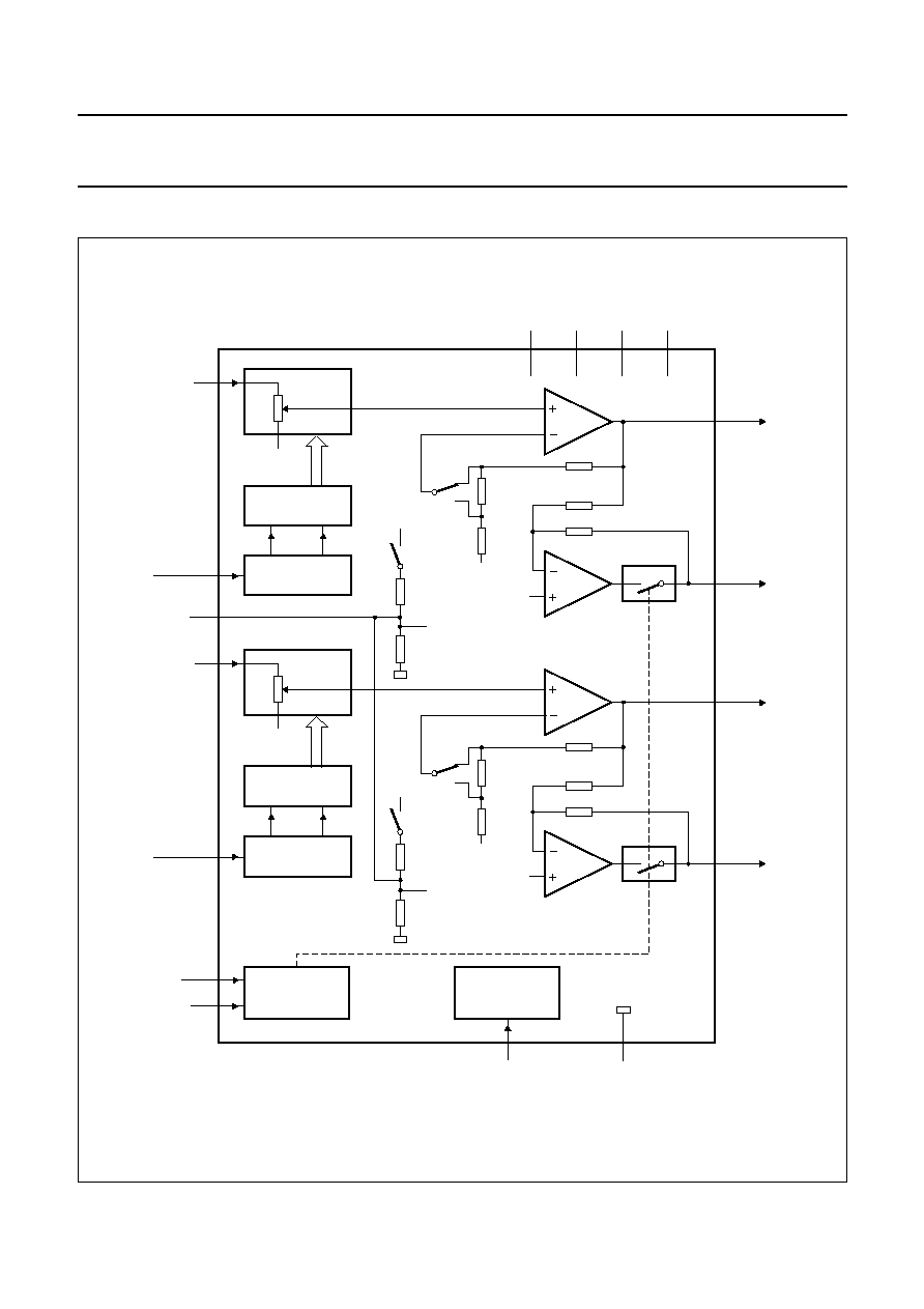
Fig.1 Block diagram.
handbook, full pagewidth
MGM608
20
k
15 k
20 k
20 k
3.4 k
1.6 k
20 dB
30 dB
20
k
15 k
20 k
20 k
3.4 k
1.6 k
15 k
15 k
15 k
15 k
20 dB
30 dB
0.5VDD
0.5VDD
0.5VDD
0.5VDD
0.5VDD
0.5VDD
VDD
VDD
0.5VDD
0.5VDD
VOLUME
CONTROL
VOLUME
CONTROL
MASTER
SLAVE
TDA8552T
MASTER
SLAVE
UP/DOWN
COUNTER
INTERFACE
UP/DOWN
COUNTER
INTERFACE
STANDBY/MUTE
AND OPERATING
GAIN
SELECTION
UP/DOWN1
UP/DOWN2
IN1
17
6
16
15
7
5
4
IN2
SVR
MODE
HPS
GAINSEL
GND1 to GND4
OUT2
-
OUT2
+
OUT1
-
OUT1
+
VDD1
VDD2
VDD3
VDD4
3
8
13
18
12
19
2
9
1, 10, 11, 20
14
up
down
up
down
1998 Jun 02
5
Philips Semiconductors
Preliminary specification
2
◊
1.4 W BTL audio amplifiers with digital
volume control and headphone sensing
TDA8552T; TDA8552TS
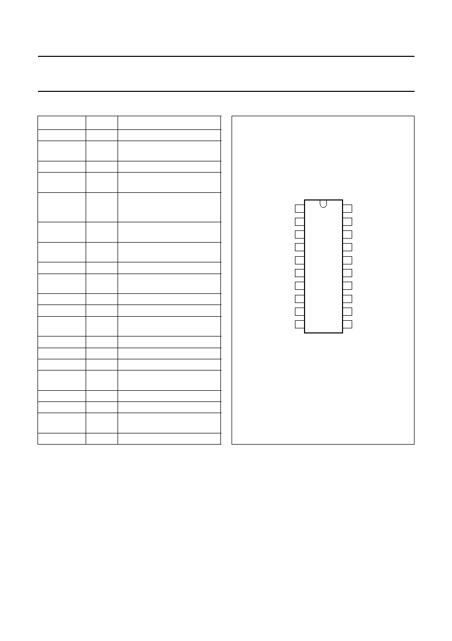
PINNING
Note
1. For the SO20 (SOT163-1) package only: the ground
pins 1, 10, 11 and 20 are mechanically connected to
the leadframe and electrically to the substrate of the
die. On the PCB the ground pins can be connected to
a copper area to decrease the thermal resistance.
SYMBOL
PIN
(1)
DESCRIPTION
GND1
1
ground 1, substrate/leadframe
OUT2+
2
positive loudspeaker terminal
output channel 2
V
DD1
3
supply voltage 1
HPS
4
digital input for headphone
sensing
MODE
5
digital trinary input for mode
selection (standby, mute and
operating)
UP/DOWN1
6
digital trinary input for volume
control channel 1
UP/DOWN2
7
digital trinary input for volume
control channel 2
V
DD2
8
supply voltage 2
OUT2
-
9
negative loudspeaker terminal
output channel 2
GND2
10
ground 2, substrate/leadframe
GND3
11
ground 3, substrate/leadframe
OUT1+
12
positive loudspeaker terminal
output channel 1
V
DD3
13
supply voltage 3
GAINSEL
14
digital input for gain selection
IN2
15
audio input channel 2
SVR
16
half supply voltage, decoupling
ripple rejection
IN1
17
audio input channel 1
V
DD4
18
supply voltage 4
OUT1
-
19
negative loudspeaker terminal
output channel 1
GND4
20
ground 4, substrate/leadframe
Fig.2 Pin configuration.
handbook, halfpage
GND1
OUT2
+
VDD1
HPS
MODE
UP/DOWN1
UP/DOWN2
VDD2
OUT2
-
GND2
GND4
OUT1
-
VDD4
IN1
IN2
GAINSEL
SVR
VDD3
OUT1
+
GND3
1
2
3
4
5
6
7
8
9
10
11
12
20
19
18
17
16
15
14
13
TDA8552T
MGM610