 | –≠–ª–µ–∫—Ç—Ä–æ–Ω–Ω—ã–π –∫–æ–º–ø–æ–Ω–µ–Ω—Ç: TDA8586TH | –°–∫–∞—á–∞—Ç—å:  PDF PDF  ZIP ZIP |
Document Outline
- FEATURES
- GENERAL DESCRIPTION
- ORDERING INFORMATION
- QUICK REFERENCE DATA
- BLOCK DIAGRAM
- PINNING
- FUNCTIONAL DESCRIPTION
- LIMITING VALUES
- THERMAL CHARACTERISTICS
- CHARACTERISTICS
- APPLICATION INFORMATION
- INTERNAL PIN CONFIGURATION
- PACKAGE OUTLINES
- SOLDERING
- DATA SHEET STATUS
- DEFINITIONS
- DISCLAIMERS

DATA SHEET
Preliminary specification
Supersedes data of 1999 Apr 08
File under Integrated Circuits, IC01
2001 Jul 23
INTEGRATED CIRCUITS
TDA8586
Power amplifier with load detection
and auto BTL/SE selection

2001 Jul 23
2
Philips Semiconductors
Preliminary specification
Power amplifier with load detection and
auto BTL/SE selection
TDA8586
FEATURES
General
∑
Operating voltage from 8 to 18 V
∑
Low distortion
∑
Few external components, fixed gain
∑
Automatic mode selection (SE or BTL) depending on
connected rear loads
∑
Can be used as a stereo amplifier in Bridge-Tied Load
(BTL) or quad Single-Ended (SE) amplifiers
∑
Single-ended mode without loudspeaker capacitor
∑
Soft clipping, to guarantee good clip behaviour with
inductive loads
∑
Mute and standby mode with one-pin operation
∑
Diagnostic information for Dynamic Distortion Detector
(DDD), high temperature (140
∞
C) operation mode and
short-circuit
∑
No switch-on/off plops when switching between standby
and mute and from mute to on
∑
Load detection on rear channels when switching from
standby to mute
∑
Fast mute on supply voltage drops (low V
P
mute).
Protection
∑
Short-circuit proof to ground, positive supply voltage on
all pins and across load
∑
ESD protected on all pins
∑
Thermal protection against temperatures exceeding
150
∞
C
∑
Load dump protection
∑
Overvoltage protection.
GENERAL DESCRIPTION
The device incorporates the following functions:
∑
4
◊
6 W SE amplifies without SE capacitor, because of
the availability of 2 half supply voltage power buffers
∑
2
◊
20 W BTL amplifiers
∑
Automatic switching between 2 and 4 speaker
operation. The mode of operation is determined during
start-up.
This amplifier is protected for all general short-circuit
conditions to battery or ground, overvoltage, 45 V load
dump and short-circuits on the speaker outputs.
The device is contained in a 20-pin power HSOP package,
but is also available in a 17-pin SIL power package. When
packaged in the 20-pin HSOP package additional
functions are available:
∑
DDD level selection between 2 and 10%
∑
Overrule pin for changing mode of operation
(from SE to BTL or from BTL to SE).
ORDERING INFORMATION
TYPE
NUMBER
PACKAGE
NAME
DESCRIPTION
VERSION
TDA8586Q
DBS17P
plastic DIL-bent-SIL power package; 17 leads (lead length 12 mm)
SOT243-1
TDA8586TH
HSOP20
heatsink small outline package; 20 leads; low stand-off
SOT418-2

2001 Jul 23
3
Philips Semiconductors
Preliminary specification
Power amplifier with load detection and
auto BTL/SE selection
TDA8586
QUICK REFERENCE DATA
SYMBOL
PARAMETER
CONDITIONS
MIN.
TYP.
MAX.
UNIT
V
P
operating supply voltage
8.0
-
18
V
I
q(tot)
total quiescent current
V
P
= 14.4 V, SE mode
-
140
170
mA
I
stb
standby supply current
V
P
= 14.4 V
-
1
100
µ
A
G
v
voltage gain
SE mode
25
26
27
dB
BTL mode
31
32
33
dB
Bridge-tied load application
P
o
output power
V
P
= 14.4 V; R
L
= 4
THD = 0.5%
14
15
-
W
THD = 10%
17
21
-
W
THD
total harmonic distortion
f
i
= 1 kHz; P
o
= 1 W;
V
P
= 14.4 V; R
L
= 4
-
0.05
0.15
%
V
OO
DC output offset voltage
V
P
= 14.4 V; R
L
= 4
;
mute condition
-
10
20
mV
V
P
= 14.4 V; on condition
-
0
100
mV
V
n(o)
noise output voltage
R
s
= 1 k
;
V
P
= 14.4 V
-
100
200
µ
V
Single-ended application
P
o
output power
V
P
= 14.4 V; R
L
= 4
THD = 0.5%
4
4.5
-
W
THD = 10%
5
6
-
W
THD
total harmonic distortion
f
i
= 1 kHz; P
o
= 1 W;
V
P
= 14.4 V; R
L
= 4
-
0.08
0.15
%
V
OO
DC output offset voltage
V
P
= 14.4 V; R
L
= 4
;
mute condition
-
10
20
mV
V
P
= 14.4 V; on condition
-
0
100
mV
V
n(o)
noise output voltage
R
s
= 1 k
;
V
P
= 14.4 V
-
80
150
µ
V

2001 Jul 23
4
Philips Semiconductors
Preliminary specification
Power amplifier with load detection and
auto BTL/SE selection
TDA8586
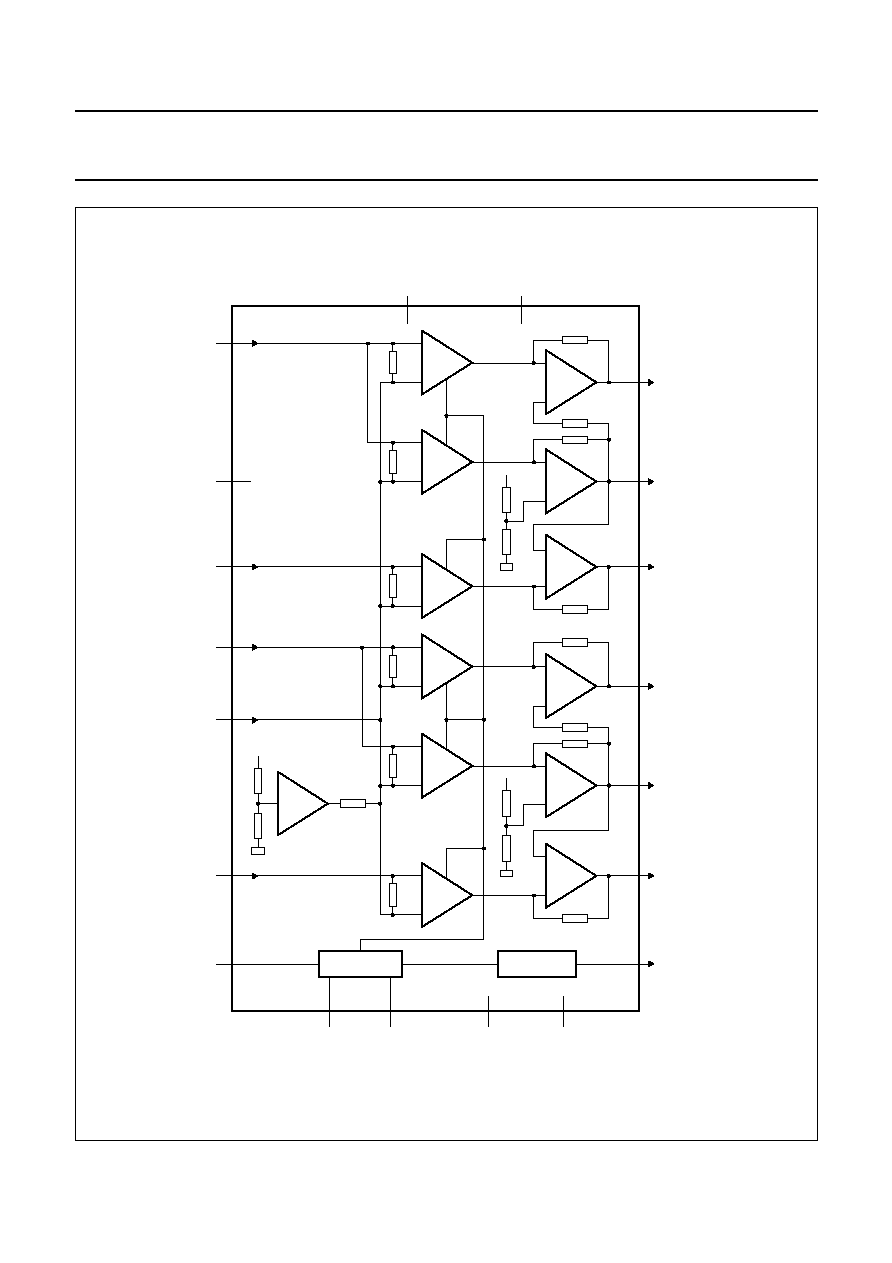
BLOCK DIAGRAM
Fig.1 Block diagram SOT243-1.
handbook, full pagewidth
MGR023
1
OUT1
ACREF
11
IN3
7
IN2
6
IN1
5
IN4
8
MSO
13
V/I
+
-
OA
+
-
4
OUT2
OA
+
-
OA
+
-
3
HVP1
VPn
VPn
60
k
V/I
+
-
60
k
V/I
+
-
60
k
17
OUT3
V/I
+
-
OA
+
-
14
OUT4
12
DIAG
OA
+
-
OA
+
-
15
HVP2
60
k
V/I
+
-
60
k
BUFFER
VPn
30 k
V/I
+
-
60
k
INTERFACE
DIAGNOSTIC
10
PGND2
VP1
2
VP2
16
9
PGND1
TDA8586Q
2001 Jul 23
5
Philips Semiconductors
Preliminary specification
Power amplifier with load detection and
auto BTL/SE selection
TDA8586
Fig.2 Block diagram SOT418-2 (HSOP20 heatsink up).
handbook, full pagewidth
MGR024
17
OUT1
ACREF
6
IN3
4
IN2
3
IN1
2
IN4
5
MSO
8
n.c.
1
V/I
+
-
OA
+
-
20
OUT2
OA
+
-
OA
+
-
19
HVP1
VPn
VPn
60
k
V/I
+
-
60
k
V/I
+
-
60
k
14
OUT3
V/I
+
-
OA
+
-
11
OUT4
7
DIAG
OA
+
-
OA
+
-
12
HVP2
60
k
V/I
+
-
60
k
BUFFER
VPn
30 k
V/I
+
-
60
k
INTERFACE
DIAGNOSTIC
10
DDDSEL
9
OVERRULE
15
PGND2
VP1
18
VP2
13
16
PGND1
TDA8586TH

2001 Jul 23
6
Philips Semiconductors
Preliminary specification
Power amplifier with load detection and
auto BTL/SE selection
TDA8586
PINNING
SYMBOL
PIN
DESCRIPTION
TDA8586Q
TDA8586TH
n.c.
-
1
not connected
IN1
5
2
non-inverting input 1
IN2
6
3
inverting input 2
IN3
7
4
non inverting input 3
IN4
8
5
inverting input 4
ACREF
11
6
common signal input
DIAG
12
7
diagnostic output/mode fix
MSO
13
8
mode select mute, standby or on
OVERRULE
-
9
mode selection overrule
DDDSEL
-
10
2 or 10% dynamic distortion detection
OUT4
14
11
SE output 4 (negative)
HVP2
15
12
buffer output/BTL output 2 (negative)
V
P2
16
13
supply voltage 2
OUT3
17
14
SE output 3/BTL output 2 (positive)
PGND2
10
15
power ground 2
PGND1
9
16
power ground 1
OUT1
1
17
SE output 1/BTL output 1 (positive)
V
P1
2
18
supply voltage 1
HVP1
3
19
buffer output/BTL output 1 (negative)
OUT2
4
20
SE output 2 (negative)
2001 Jul 23
7
Philips Semiconductors
Preliminary specification
Power amplifier with load detection and
auto BTL/SE selection
TDA8586
Fig.3 Pin configuration (SOT243-1).
handbook, halfpage
TDA8586Q
MGR025
OUT1
VP1
HVP1
OUT2
IN1
IN2
IN3
IN4
PGND1
PGND2
ACREF
DIAG
MSO
OUT4
HVP2
VP2
OUT3
1
2
3
4
5
6
7
8
9
10
11
12
13
14
15
16
17
Fig.4 Pin configuration (SOT418-2).
handbook, halfpage
n.c.
IN1
IN2
IN3
IN4
ACREF
DIAG
MSO
OVERRULE
DDDSEL
OUT2
HVP1
VP1
OUT1
PGND2
OUT3
PGND1
VP2
HVP2
OUT4
TDA8586TH
MGR026
1
2
3
4
5
6
7
8
9
10
20
19
18
17
16
15
14
13
12
11

2001 Jul 23
8
Philips Semiconductors
Preliminary specification
Power amplifier with load detection and
auto BTL/SE selection
TDA8586
FUNCTIONAL DESCRIPTION
The TDA8586 is a multi-purpose power amplifier with four
amplifiers and 2 buffer stages, which can be connected in
the following configurations with high output power and
low distortion:
∑
Dual Bridge-Tied Load (BTL) amplifiers
∑
Quad Single-Ended (SE) amplifiers.
In the BTL mode of operation, the 2 buffer amplifiers act as
inverting amplifiers to complete the bridge across the front
amplifiers (OUT1 and OUT3) and the rear outputs (OUT2
and OUT4) enter a high-impedance state.
In the SE mode of operation, the buffers act as an AC
ground path thereby eliminating the need for series
capacitors on the speaker outputs.
Diagnostics:
∑
While the IC is in the mute mode, the diagnostic output
will signal the mode of operation when the IC is not
overruled
∑
In the on mode the diagnostic output will signal any fault
in the IC or if the output of any amplifier is clipping with
a distortion of 10% (or 2% depending on selected
clip-mode).
Special attention is given to the dynamic behaviour as
follows:
∑
Noise suppression during engine start
∑
No plops when switching from standby to on
∑
Slow offset change between mute and on (controlled by
MSO pin)
∑
Low noise levels, which are independent of the supply
voltage.
Protections are included to avoid the IC being damaged at:
∑
Over temperature: T
j
> 150
∞
C
∑
Short-circuit of the output pin(s) to ground or supply rail.
When short-circuited, the power dissipation is limited
∑
ESD protection (Human Body Model 3000 V and
Machine Model 300 V).
The presence of the load is measured after the transition
between standby and mute. The IC will determine if there
is an acceptable load on both outputs (OUT2 and OUT4).
If both outputs are unloaded, the IC will switch to a
2 speaker mode of operation (BTL mode), unless it is
overruled.
There are two options to overrule:
1. Before transition from mute to on, after a load
detection, pulling the diagnostic output above 9.5 V
will force the IC into 4 speaker mode
2. TDA8586TH: pulling the OVERRULE pin according
pinning table.
Care should be taken with the OVERRULE function as it
works during the on mode. If there is a 2 or 4 speaker
mode change during the on mode a large plop can be
heard on the speakers.
The ACREF input (common signal input) acts with the four
signal inputs (IN1 to IN4) to provide quasi differential
inputs. A capacitor must be connected to this pin of which
the ground pin should be connected to the ground at the
signal source (usually the ground at the audio signal
processor). This capacitor has a dual function. During the
speaker detection, the signal ground capacitor is used to
set the time constant of the measurement (and thus
determines the minimum required switch-on time).
The capacitor on the MSO pin allows the integrate function
to provide immunity to outside noises during load
detection.

2001 Jul 23
9
Philips Semiconductors
Preliminary specification
Power amplifier with load detection and
auto BTL/SE selection
TDA8586
Fig.5 Timing diagram including diagnostics.
handbook, full pagewidth
MGR027
state
condition
This voltage must remain present.
Whatever the load detection has found the mode of operation will be inverted.
Toggling between the 2 modes is possible.
The mode is overruled only from
BTL to SE when the diagnostic pin
is excited with a pulse of 10 V.
standby
load detect
mute
no load detect
mute
no clipping/shorts
on
clipping
on
short-circuit
on
VP
VP
MSO
diagnostic
information
diagnostic
overrule
mode select
amplifier
output
buffer/amplifier
output
0
0
3 V
5 V
10 V
0
5 V
0
0.5VP
0
0.5VP
0
0
9 V
short-circuit to supply
short-circuit over load
short-circuit to ground
short-circuit to supply
short-circuit over load
short-circuit to ground
SE detected
BTL detected
SE detection
BTL detection
minimum 1 s

2001 Jul 23
10
Philips Semiconductors
Preliminary specification
Power amplifier with load detection and
auto BTL/SE selection
TDA8586
LIMITING VALUES
In accordance with the Absolute Maximum Rating System (IEC 60134).
Note
1. A large reverse current will flow, therefore external protection is needed (fuse and reverse diode).
SYMBOL
PARAMETER
CONDITIONS
MIN.
MAX.
UNIT
V
P
supply voltage
operating
8
18
V
load dump protected;
see Fig.6
-
45
V
V
DIAG
voltage on diagnostic pin
-
18
V
I
OSM
non-repetitive peak output current
-
6
A
I
ORM
repetitive peak output current
-
4
A
V
rp
reverse polarity voltage
note 1
-
6
V
V
sc
AC and DC short-circuit voltage of output pins
across loads and to ground or supply pins
-
18
V
P
tot
total power dissipation
-
75
W
T
j
junction temperature
-
150
∞
C
T
stg
storage temperature
-
55
+150
∞
C
T
amb
operating ambient temperature
-
40
+150
∞
C
Fig.6 Load dump voltage waveform.
handbook, halfpage
MGL404
tr
VP
tf
45 V
14.4 V
t (ms)
THERMAL CHARACTERISTICS
SYMBOL
PARAMETER
CONDITIONS
VALUE
UNIT
R
th(j-a)
thermal resistance from junction to ambient
in free air
40
K/W
R
th(j-c)
thermal resistance from junction to case
2
K/W

2001 Jul 23
11
Philips Semiconductors
Preliminary specification
Power amplifier with load detection and
auto BTL/SE selection
TDA8586
CHARACTERISTICS
V
P
= 14.4 V; T
amb
= 25
∞
C; f
i
= 1 kHz; R
L
=
; measured in test circuit of Fig.8; unless otherwise specified.
SYMBOL
PARAMETER
CONDITIONS
MIN.
TYP.
MAX.
UNIT
Supplies
V
P
operating supply voltage
8.0
14.4
18
V
I
q(tot)
total quiescent current
SE mode
-
140
170
mA
I
stb
standby current
-
1
100
µ
A
V
O
DC output voltage
V
P
= 14.4 V
-
7.0
-
V
V
P(mute)
low supply voltage mute
6.0
7.0
8.0
V
V
o
single-ended and bridge-tied
load output voltage
V
P
= 14.4 V; R
L
= 4
mute condition
-
-
20
mV
on condition
-
-
100
mV
V
I
DC input voltage
V
P
= 14.4 V
-
4.0
-
V
P
IN
MSO
V
MSO
voltage at pin MSO
standby condition
0
-
0.8
V
mute condition; note 1
2.0
3.0
4
V
on condition
8.0
-
10.5
V
I
MSO
input current
mute pin at standby condition;
V
MSO
< 0.8 V
-
5
40
µ
A
Diagnostic; output buffer (open-collector); see Figs 7 to 8
V
DIAG(L)
diagnostic output voltage LOW I
sink
= 1 mA
-
0.3
0.8
V
I
LI
leakage current
V
DIAG
= 14.4 V
-
-
1
µ
A
V
DIAG(or)
diagnostic override voltage
in mute mode after load
detection
10.5
-
18
V
V
DIAG(4ch)
diagnostic 4 channel indication
voltage
mute, after load detection with
4 speakers connected
-
0.3
0.8
V
CD2
clip detector LOW
THD mode; V
DIAG
> 3 V;
R = 10 k
0.5
2
3.5
%
CD10
clip detector HIGH
THD mode (default);
V
DIAG
> 3 V; R = 10 k
7
10
13
%
C
LIP DETECT CONTROL PIN
V
DDDSEL
voltage at DDD select pin to
obtain:
10% DDD
0
-
1
V
2% DDD
3
-
6
V
I
DDDSEL
Input current DDD select pin
V
DDDSEL
= 5 V
15
-
140
µ
A
Stereo BTL application (see Fig.7)
THD
total harmonic distortion
f
i
= 1 kHz; P
o
= 1 W; R
L
= 4
-
0.05
0.15
%
45 Hz < f
i
< 10 kHz; P
o
= 1 W;
R
L
= 4
; filter: f < 30 kHz
-
0.3
-
%
P
o
output power
V
P
= 14.4 V; R
L
= 4
; note 2
THD = 0.5%
14
15
-
W
THD = 10%
17
21
-
W

2001 Jul 23
12
Philips Semiconductors
Preliminary specification
Power amplifier with load detection and
auto BTL/SE selection
TDA8586
Notes
1. Tolerances on the mute level is tight because of the usage of this pin for integration during load detection.
2. The output power is measured directly on the pins of the IC.
3. The noise output is measured in a bandwidth of 20 Hz to 20 kHz.
G
v
voltage gain
V
i(rms)
= 15 mV
31
32
33
dB
G
v
channel unbalance
V
i(rms)
= 15 mV
-
0.7
0
+0.7
dB
cs
channel separation
P
o
= 2 W; f
i
= 1 kHz; R
L
= 4
45
55
-
dB
V
OO
DC output offset voltage
V
P
= 14.4 V; on condition
-
0
100
mV
V
P
= 14.4 V; R
L
= 4
;
mute condition
-
10
20
mV
V
n(o)
noise output voltage on
R
s
= 1 k
; V
P
= 14.4 V; note 3
-
100
150
µ
V
V
n(o)(mute)
noise output voltage mute
note 3
-
0
20
µ
V
V
o(mute)
output voltage mute
V
i(rms)
= 1 V
-
3
500
µ
V
SVRR
supply voltage ripple rejection: R
s
= 0
; f
i
= 1 kHz;
V
ripple
= 2 V (p-p)
on condition
45
55
-
dB
mute condition
55
70
-
dB
Z
i
input impedance
input referenced to ground
40
60
90
k
Quad SE application (see Fig.8)
THD
total harmonic distortion
f
i
= 1 kHz; P
o
= 1 W; R
L
= 4
-
0.05
0.15
%
45 Hz < f
i
< 10 kHz; P
o
= 1 W;
R
L
= 4
; filter: f < 30 kHz
-
0.5
-
%
P
o
output power
V
P
= 14.4 V; R
L
= 4
; note 2
THD = 0.5%
4
4.5
-
W
THD = 10%
5
6
-
W
G
v
voltage gain
V
i(rms)
= 15 mV
25
26
27
dB
G
v
channel unbalance
V
i(rms)
= 15 mV
-
0.7
0
+0.7
dB
cs
channel separation
P
o
= 2 W; f
i
= 1 kHz; R
L
= 4
40
50
-
dB
V
OO
DC output offset voltage
V
P
= 14.4 V; on condition
-
0
100
mV
V
P
= 14.4 V; R
L
= 4
;
mute condition
-
10
20
mV
V
n(o)
noise output voltage on
R
s
= 1 k
; V
P
= 14.4 V; note 3
-
80
150
µ
V
V
n(o)(mute)
noise output voltage mute
note 3
-
0
20
µ
V
V
o(mute)
output voltage mute
V
i(rms)
= 1 V
-
3
500
µ
V
SVRR
supply voltage ripple rejection
R
s
= 0
; f
i
= 1 kHz;
V
ripple
= 2 V (p-p)
on condition
43
47
-
dB
mute condition
55
70
-
dB
SYMBOL
PARAMETER
CONDITIONS
MIN.
TYP.
MAX.
UNIT
2001 Jul 23
13
Philips Semiconductors
Preliminary specification
Power amplifier with load detection and
auto BTL/SE selection
TDA8586
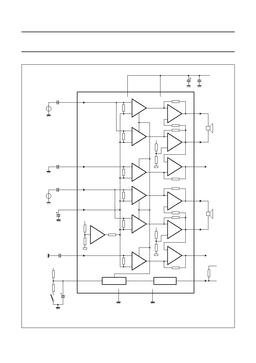
APPLICATION INFORMATION
Fig.7 Stereo bridge-tied load application (SOT243-1).
handbook, full pagewidth
MGR028
1 OUT1
11
IN3 7
IN2 6
IN1 5
IN4 8
13
V/I
+
-
OA
+
-
4 OUT2
OA
+
-
OA
+
-
3 HVP1
VPn
VPn
60
k
V/I
+
-
60
k
V/I
+
-
60
k
17 OUT3
V/I
+
-
OA
+
-
14 OUT4
12
OA
+
-
OA
+
-
15 HVP2
60
k
V/I
+
-
60
k
BUFFER
VPn
30 k
V/I
+
-
60
k
INTERFACE
DIAGNOSTIC
10
PGND2
VP1
2
VP2
16
9
PGND1
TDA8586Q
+
-
4 or 8
+
-
4 or 8
100
nF
(16/40 V)
1000
µ
F
VP
+
5 V
10 k
VINL front
220 nF
VINR front
220 nF
47
µ
F
(10 V)
15 k
30 k
4.7
µ
F
(10 V)
switch
switched
+
9 V
220 nF
220 nF
ACREF
MSO
DIAG

2001 Jul 23
14
Philips Semiconductors
Preliminary specification
Power amplifier with load detection and
auto BTL/SE selection
TDA8586
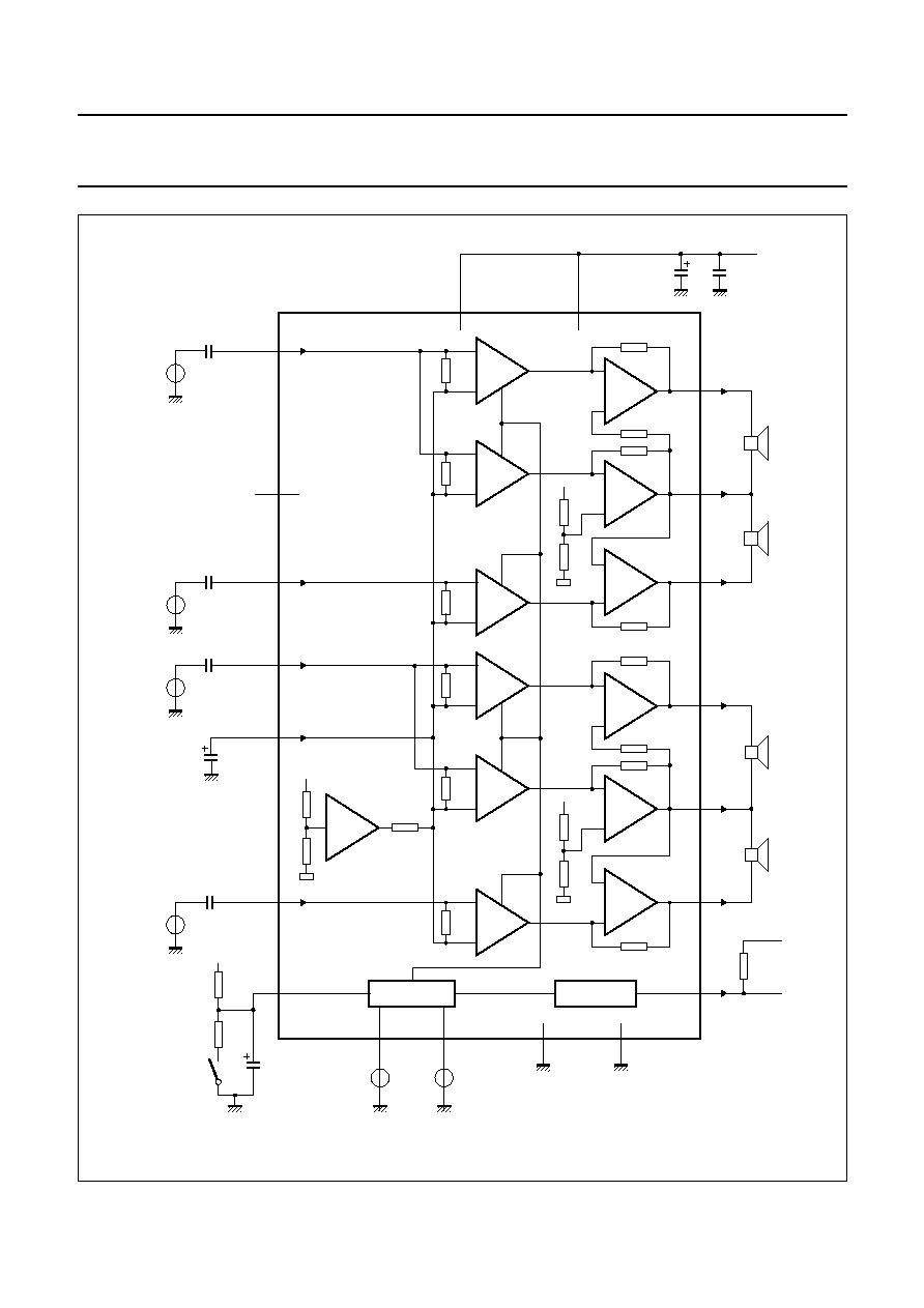
Fig.8 Quad single-ended application (SOT243-1).
handbook, full pagewidth
MGR029
1 OUT1
ACREF 11
IN3 7
IN2 6
IN1 5
IN4 8
MSO 13
V/I
+
-
OA
+
-
4 OUT2
OA
+
-
OA
+
-
3 HVP1
VPn
VPn
60
k
V/I
+
-
60
k
V/I
+
-
60
k
17 OUT3
V/I
+
-
OA
+
-
14 OUT4
12 DIAG
OA
+
-
OA
+
-
15 HVP2
60
k
V/I
+
-
60
k
BUFFER
VPn
30 k
V/I
+
-
60
k
INTERFACE
DIAGNOSTIC
PGND2
VP1
2
VP2
16
9
PGND1
TDA8586Q
+
-
+
-
4 or 8
4 or 8
+
-
+
-
4 or 8
4 or 8
100
nF
(16/40 V)
1000
µ
F
VP
+
5 V
10 k
VINL front
220 nF
VINL rear
220 nF
VINR front
220 nF
47
µ
F
(10 V)
VINR rear
220 nF
15 k
30 k
4.7
µ
F
(10 V)
switch
switched
+
9 V
10

2001 Jul 23
15
Philips Semiconductors
Preliminary specification
Power amplifier with load detection and
auto BTL/SE selection
TDA8586
Fig.9 Stereo bridge-tied load application (SOT418-2).
handbook, full pagewidth
MGR030
17 OUT1
ACREF 6
IN3 4
IN2 3
IN1 2
IN4 5
MSO 8
V/I
+
-
OA
+
-
20 OUT2
OA
+
-
OA
+
-
19 HVP1
VPn
VPn
60
k
V/I
+
-
60
k
V/I
+
-
60
k
14 OUT3
V/I
+
-
OA
+
-
11 OUT4
7 DIAG
OA
+
-
OA
+
-
12 HVP2
60
k
V/I
+
-
60
k
BUFFER
VPn
30 k
V/I
+
-
60
k
INTERFACE
DIAGNOSTIC
10
DDDSEL
9
OVERRULE
15
PGND2
VP1
18
VP2
13
16
PGND1
TDA8586TH
+
-
4 or 8
+
-
4 or 8
100
nF
(16/40 V)
1000
µ
F
VP
+
5 V
10 k
VINL front
220 nF
VINR front
220 nF
47
µ
F
(10 V)
15 k
30 k
4.7
µ
F
(10 V)
switch
switched
+
9 V
n.c. 1
220 nF
220 nF
2001 Jul 23
16
Philips Semiconductors
Preliminary specification
Power amplifier with load detection and
auto BTL/SE selection
TDA8586
Fig.10 Quad single-ended application (SOT418-2).
handbook, full pagewidth
MGR031
17 OUT1
ACREF 6
IN3 4
IN2 3
IN1 2
IN4 5
MSO 8
V/I
+
-
OA
+
-
20 OUT2
OA
+
-
OA
+
-
19 HVP1
VPn
VPn
60
k
V/I
+
-
60
k
V/I
+
-
60
k
14 OUT3
V/I
+
-
OA
+
-
11 OUT4
7 DIAG
OA
+
-
OA
+
-
12 HVP2
60
k
V/I
+
-
60
k
BUFFER
VPn
30 k
V/I
+
-
60
k
INTERFACE
DIAGNOSTIC
10
DDDSEL
9
OVERRULE
15
PGND2
VP1
18
VP2
13
16
PGND1
TDA8586TH
+
-
+
-
4 or 8
4 or 8
+
-
+
-
4 or 8
4 or 8
100
nF
(16/40 V)
1000
µ
F
VP
+
5 V
10 k
VINL front
220 nF
VINL rear
220 nF
VINR front
220 nF
47
µ
F
(10 V)
VINR rear
220 nF
15 k
30 k
4.7
µ
F
(10 V)
switch
switched
+
9 V
n.c.
1

2001 Jul 23
17
Philips Semiconductors
Preliminary specification
Power amplifier with load detection and
auto BTL/SE selection
TDA8586
INTERNAL PIN CONFIGURATION
PIN
TDA8586TH
NAME
EQUIVALENT CIRCUIT
2, 3, 4, 5 and 6
inputs
11, 12, 14, 17,
19 and 20
outputs
8
mode select
handbook, halfpage
MGE014
VP
IN
handbook, halfpage
MGE015
VP
OUT
0.5 VP
handbook, halfpage
MGE016
VP
2001 Jul 23
18
Philips Semiconductors
Preliminary specification
Power amplifier with load detection and
auto BTL/SE selection
TDA8586
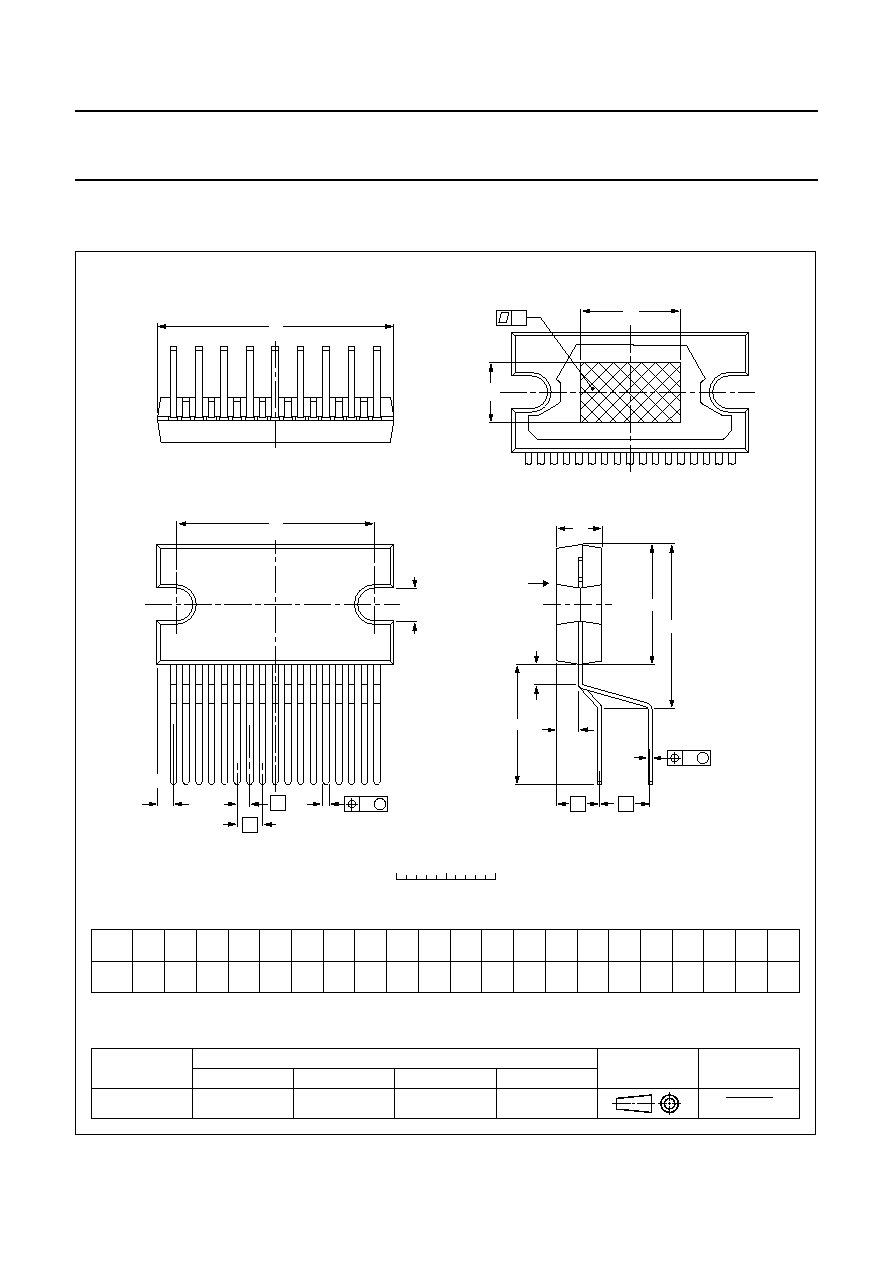
PACKAGE OUTLINES
REFERENCES
OUTLINE
VERSION
EUROPEAN
PROJECTION
ISSUE DATE
IEC
JEDEC
EIAJ
DIMENSIONS (mm are the original dimensions)
Note
1. Plastic or metal protrusions of 0.25 mm maximum per side are not included.
SOT243-1
0
5
10 mm
scale
D
L
E
A
c
A
2
L
3
Q
w
M
b
p
1
d
D
Z
e
e
x
h
1
17
j
Eh
non-concave
97-12-16
99-12-17
DBS17P: plastic DIL-bent-SIL power package; 17 leads (lead length 12 mm)
SOT243-1
view B: mounting base side
m
2
e
v
M
B
UNIT
A
e
1
A
2
b
p
c
D
(1)
E
(1)
Z
(1)
d
e
D
h
L
L
3
m
mm
17.0
15.5
4.6
4.4
0.75
0.60
0.48
0.38
24.0
23.6
20.0
19.6
10
2.54
v
0.8
12.2
11.8
1.27
e
2
5.08
2.4
1.6
E
h
6
2.00
1.45
2.1
1.8
3.4
3.1
4.3
12.4
11.0
Q
j
0.4
w
0.03
x

2001 Jul 23
19
Philips Semiconductors
Preliminary specification
Power amplifier with load detection and
auto BTL/SE selection
TDA8586
UNIT
A4
(1)
REFERENCES
OUTLINE
VERSION
EUROPEAN
PROJECTION
ISSUE DATE
98-02-25
99-11-12
IEC
JEDEC
EIAJ
mm
+
0.12
-
0.02
3.5
0.35
DIMENSIONS (mm are the original dimensions)
Notes
1. Limits per individual lead.
2. Plastic or metal protrusions of 0.25 mm maximum per side are not included.
SOT418-2
0
5
10 mm
scale
HSOP20: plastic, heatsink small outline package; 20 leads; low stand-off height
SOT418-2
A
max.
detail X
A2
3.5
3.2
D2
1.1
0.9
HE
14.5
13.9
Lp
1.1
0.8
Q
1.7
1.5
2.5
2.0
v
0.25
w
0.25
y
Z
8
∞
0
∞
0.07
x
0.03
D1
13.0
12.6
E1
6.2
5.8
E2
2.9
2.5
bp
c
0.32
0.23
e
1.27
D
(2)
16.0
15.8
E
(2)
11.1
10.9
0.53
0.40
A3
A4
A2
(A3)
Lp
A
Q
D
y
x
HE
E
c
v
M
A
X
A
bp
w
M
Z
D1
D2
E2
E1
e
20
11
1
10
pin 1 index

2001 Jul 23
20
Philips Semiconductors
Preliminary specification
Power amplifier with load detection and
auto BTL/SE selection
TDA8586
SOLDERING
Introduction
This text gives a very brief insight to a complex technology.
A more in-depth account of soldering ICs can be found in
our
"Data Handbook IC26; Integrated Circuit Packages"
(document order number 9398 652 90011).
There is no soldering method that is ideal for all IC
packages. Wave soldering is often preferred when
through-hole and surface mount components are mixed on
one printed-circuit board. Wave soldering can still be used
for certain surface mount ICs, but it is not suitable for fine
pitch SMDs. In these situations reflow soldering is
recommended.
Through-hole mount packages
S
OLDERING BY DIPPING OR BY SOLDER WAVE
The maximum permissible temperature of the solder is
260
∞
C; solder at this temperature must not be in contact
with the joints for more than 5 seconds. The total contact
time of successive solder waves must not exceed
5 seconds.
The device may be mounted up to the seating plane, but
the temperature of the plastic body must not exceed the
specified maximum storage temperature (T
stg(max)
). If the
printed-circuit board has been pre-heated, forced cooling
may be necessary immediately after soldering to keep the
temperature within the permissible limit.
M
ANUAL SOLDERING
Apply the soldering iron (24 V or less) to the lead(s) of the
package, either below the seating plane or not more than
2 mm above it. If the temperature of the soldering iron bit
is less than 300
∞
C it may remain in contact for up to
10 seconds. If the bit temperature is between
300 and 400
∞
C, contact may be up to 5 seconds.
Surface mount packages
R
EFLOW SOLDERING
Reflow soldering requires solder paste (a suspension of
fine solder particles, flux and binding agent) to be applied
to the printed-circuit board by screen printing, stencilling or
pressure-syringe dispensing before package placement.
Several methods exist for reflowing; for example,
convection or convection/infrared heating in a conveyor
type oven. Throughput times (preheating, soldering and
cooling) vary between 100 and 200 seconds depending
on heating method.
Typical reflow peak temperatures range from
215 to 250
∞
C. The top-surface temperature of the
packages should preferable be kept below 220
∞
C for
thick/large packages, and below 235
∞
C for small/thin
packages.
W
AVE SOLDERING
Conventional single wave soldering is not recommended
for surface mount devices (SMDs) or printed-circuit boards
with a high component density, as solder bridging and
non-wetting can present major problems.
To overcome these problems the double-wave soldering
method was specifically developed.
If wave soldering is used the following conditions must be
observed for optimal results:
∑
Use a double-wave soldering method comprising a
turbulent wave with high upward pressure followed by a
smooth laminar wave.
∑
For packages with leads on two sides and a pitch (e):
≠ larger than or equal to 1.27 mm, the footprint
longitudinal axis is preferred to be parallel to the
transport direction of the printed-circuit board;
≠ smaller than 1.27 mm, the footprint longitudinal axis
must be parallel to the transport direction of the
printed-circuit board.
The footprint must incorporate solder thieves at the
downstream end.
∑
For packages with leads on four sides, the footprint must
be placed at a 45
∞
angle to the transport direction of the
printed-circuit board. The footprint must incorporate
solder thieves downstream and at the side corners.
During placement and before soldering, the package must
be fixed with a droplet of adhesive. The adhesive can be
applied by screen printing, pin transfer or syringe
dispensing. The package can be soldered after the
adhesive is cured.
Typical dwell time is 4 seconds at 250
∞
C.
A mildly-activated flux will eliminate the need for removal
of corrosive residues in most applications.
M
ANUAL SOLDERING
Fix the component by first soldering two
diagonally-opposite end leads. Use a low voltage (24 V or
less) soldering iron applied to the flat part of the lead.
Contact time must be limited to 10 seconds at up to
300
∞
C. When using a dedicated tool, all other leads can
be soldered in one operation within 2 to 5 seconds
between 270 and 320
∞
C.

2001 Jul 23
21
Philips Semiconductors
Preliminary specification
Power amplifier with load detection and
auto BTL/SE selection
TDA8586
Suitability of IC packages for wave, reflow and dipping soldering methods
Notes
1. All surface mount (SMD) packages are moisture sensitive. Depending upon the moisture content, the maximum
temperature (with respect to time) and body size of the package, there is a risk that internal or external package
cracks may occur due to vaporization of the moisture in them (the so called popcorn effect). For details, refer to the
Drypack information in the
"Data Handbook IC26; Integrated Circuit Packages; Section: Packing Methods".
2. For SDIP packages, the longitudinal axis must be parallel to the transport direction of the printed-circuit board.
3. These packages are not suitable for wave soldering as a solder joint between the printed-circuit board and heatsink
(at bottom version) can not be achieved, and as solder may stick to the heatsink (on top version).
4. If wave soldering is considered, then the package must be placed at a 45
∞
angle to the solder wave direction.
The package footprint must incorporate solder thieves downstream and at the side corners.
5. Wave soldering is only suitable for LQFP, QFP and TQFP packages with a pitch (e) equal to or larger than 0.8 mm;
it is definitely not suitable for packages with a pitch (e) equal to or smaller than 0.65 mm.
6. Wave soldering is only suitable for SSOP and TSSOP packages with a pitch (e) equal to or larger than 0.65 mm; it is
definitely not suitable for packages with a pitch (e) equal to or smaller than 0.5 mm.
MOUNTING
PACKAGE
SOLDERING METHOD
WAVE
REFLOW
(1)
DIPPING
Through-hole mount DBS, DIP, HDIP, SDIP, SIL
suitable
(2)
-
suitable
Surface mount
BGA, HBGA, LFBGA, SQFP, TFBGA
not suitable
suitable
-
HBCC, HLQFP, HSQFP, HSOP, HTQFP,
HTSSOP, HVQFN, SMS
not suitable
(3)
suitable
-
PLCC
(4)
, SO, SOJ
suitable
suitable
-
LQFP, QFP, TQFP
not recommended
(4)(5)
suitable
-
SSOP, TSSOP, VSO
not recommended
(6)
suitable
-

2001 Jul 23
22
Philips Semiconductors
Preliminary specification
Power amplifier with load detection and
auto BTL/SE selection
TDA8586
DATA SHEET STATUS
Notes
1. Please consult the most recently issued data sheet before initiating or completing a design.
2. The product status of the device(s) described in this data sheet may have changed since this data sheet was
published. The latest information is available on the Internet at URL http://www.semiconductors.philips.com.
DATA SHEET STATUS
(1)
PRODUCT
STATUS
(2)
DEFINITIONS
Objective data
Development
This data sheet contains data from the objective specification for product
development. Philips Semiconductors reserves the right to change the
specification in any manner without notice.
Preliminary data
Qualification
This data sheet contains data from the preliminary specification.
Supplementary data will be published at a later date. Philips
Semiconductors reserves the right to change the specification without
notice, in order to improve the design and supply the best possible
product.
Product data
Production
This data sheet contains data from the product specification. Philips
Semiconductors reserves the right to make changes at any time in order
to improve the design, manufacturing and supply. Changes will be
communicated according to the Customer Product/Process Change
Notification (CPCN) procedure SNW-SQ-650A.
DEFINITIONS
Short-form specification
The data in a short-form
specification is extracted from a full data sheet with the
same type number and title. For detailed information see
the relevant data sheet or data handbook.
Limiting values definition
Limiting values given are in
accordance with the Absolute Maximum Rating System
(IEC 60134). Stress above one or more of the limiting
values may cause permanent damage to the device.
These are stress ratings only and operation of the device
at these or at any other conditions above those given in the
Characteristics sections of the specification is not implied.
Exposure to limiting values for extended periods may
affect device reliability.
Application information
Applications that are
described herein for any of these products are for
illustrative purposes only. Philips Semiconductors make
no representation or warranty that such applications will be
suitable for the specified use without further testing or
modification.
DISCLAIMERS
Life support applications
These products are not
designed for use in life support appliances, devices, or
systems where malfunction of these products can
reasonably be expected to result in personal injury. Philips
Semiconductors customers using or selling these products
for use in such applications do so at their own risk and
agree to fully indemnify Philips Semiconductors for any
damages resulting from such application.
Right to make changes
Philips Semiconductors
reserves the right to make changes, without notice, in the
products, including circuits, standard cells, and/or
software, described or contained herein in order to
improve design and/or performance. Philips
Semiconductors assumes no responsibility or liability for
the use of any of these products, conveys no licence or title
under any patent, copyright, or mask work right to these
products, and makes no representations or warranties that
these products are free from patent, copyright, or mask
work right infringement, unless otherwise specified.

2001 Jul 23
23
Philips Semiconductors
Preliminary specification
Power amplifier with load detection and
auto BTL/SE selection
TDA8586
NOTES

© Philips Electronics N.V.
SCA
All rights are reserved. Reproduction in whole or in part is prohibited without the prior written consent of the copyright owner.
The information presented in this document does not form part of any quotation or contract, is believed to be accurate and reliable and may be changed
without notice. No liability will be accepted by the publisher for any consequence of its use. Publication thereof does not convey nor imply any license
under patent- or other industrial or intellectual property rights.
Internet: http://www.semiconductors.philips.com
2001
72
Philips Semiconductors ≠ a worldwide company
For all other countries apply to: Philips Semiconductors,
Marketing Communications, Building BE-p, P.O. Box 218, 5600 MD EINDHOVEN,
The Netherlands, Fax. +31 40 27 24825
Argentina: see South America
Australia: 3 Figtree Drive, HOMEBUSH, NSW 2140,
Tel. +61 2 9704 8141, Fax. +61 2 9704 8139
Austria: Computerstr. 6, A-1101 WIEN, P.O. Box 213,
Tel. +43 1 60 101 1248, Fax. +43 1 60 101 1210
Belarus: Hotel Minsk Business Center, Bld. 3, r. 1211, Volodarski Str. 6,
220050 MINSK, Tel. +375 172 20 0733, Fax. +375 172 20 0773
Belgium: see The Netherlands
Brazil: see South America
Bulgaria: Philips Bulgaria Ltd., Energoproject, 15th floor,
51 James Bourchier Blvd., 1407 SOFIA,
Tel. +359 2 68 9211, Fax. +359 2 68 9102
Canada: PHILIPS SEMICONDUCTORS/COMPONENTS,
Tel. +1 800 234 7381, Fax. +1 800 943 0087
China/Hong Kong: 501 Hong Kong Industrial Technology Centre,
72 Tat Chee Avenue, Kowloon Tong, HONG KONG,
Tel. +852 2319 7888, Fax. +852 2319 7700
Colombia: see South America
Czech Republic: see Austria
Denmark: Sydhavnsgade 23, 1780 COPENHAGEN V,
Tel. +45 33 29 3333, Fax. +45 33 29 3905
Finland: Sinikalliontie 3, FIN-02630 ESPOO,
Tel. +358 9 615 800, Fax. +358 9 6158 0920
France: 7 - 9 Rue du Mont ValÈrien, BP317, 92156 SURESNES Cedex,
Tel. +33 1 4728 6600, Fax. +33 1 4728 6638
Germany: Hammerbrookstraþe 69, D-20097 HAMBURG,
Tel. +49 40 2353 60, Fax. +49 40 2353 6300
Hungary: Philips Hungary Ltd., H-1119 Budapest, Fehervari ut 84/A,
Tel: +36 1 382 1700, Fax: +36 1 382 1800
India: Philips INDIA Ltd, Band Box Building, 2nd floor,
254-D, Dr. Annie Besant Road, Worli, MUMBAI 400 025,
Tel. +91 22 493 8541, Fax. +91 22 493 0966
Indonesia: PT Philips Development Corporation, Semiconductors Division,
Gedung Philips, Jl. Buncit Raya Kav.99-100, JAKARTA 12510,
Tel. +62 21 794 0040 ext. 2501, Fax. +62 21 794 0080
Ireland: Newstead, Clonskeagh, DUBLIN 14,
Tel. +353 1 7640 000, Fax. +353 1 7640 200
Israel: RAPAC Electronics, 7 Kehilat Saloniki St, PO Box 18053,
TEL AVIV 61180, Tel. +972 3 645 0444, Fax. +972 3 649 1007
Italy: PHILIPS SEMICONDUCTORS, Via Casati, 23 - 20052 MONZA (MI),
Tel. +39 039 203 6838, Fax +39 039 203 6800
Japan: Philips Bldg 13-37, Kohnan 2-chome, Minato-ku,
TOKYO 108-8507, Tel. +81 3 3740 5130, Fax. +81 3 3740 5057
Korea: Philips House, 260-199 Itaewon-dong, Yongsan-ku, SEOUL,
Tel. +82 2 709 1412, Fax. +82 2 709 1415
Malaysia: No. 76 Jalan Universiti, 46200 PETALING JAYA, SELANGOR,
Tel. +60 3 750 5214, Fax. +60 3 757 4880
Mexico: 5900 Gateway East, Suite 200, EL PASO, TEXAS 79905,
Tel. +9-5 800 234 7381, Fax +9-5 800 943 0087
Middle East: see Italy
Netherlands: Postbus 90050, 5600 PB EINDHOVEN, Bldg. VB,
Tel. +31 40 27 82785, Fax. +31 40 27 88399
New Zealand: 2 Wagener Place, C.P.O. Box 1041, AUCKLAND,
Tel. +64 9 849 4160, Fax. +64 9 849 7811
Norway: Box 1, Manglerud 0612, OSLO,
Tel. +47 22 74 8000, Fax. +47 22 74 8341
Pakistan: see Singapore
Philippines: Philips Semiconductors Philippines Inc.,
106 Valero St. Salcedo Village, P.O. Box 2108 MCC, MAKATI,
Metro MANILA, Tel. +63 2 816 6380, Fax. +63 2 817 3474
Poland: Al.Jerozolimskie 195 B, 02-222 WARSAW,
Tel. +48 22 5710 000, Fax. +48 22 5710 001
Portugal: see Spain
Romania: see Italy
Russia: Philips Russia, Ul. Usatcheva 35A, 119048 MOSCOW,
Tel. +7 095 755 6918, Fax. +7 095 755 6919
Singapore: Lorong 1, Toa Payoh, SINGAPORE 319762,
Tel. +65 350 2538, Fax. +65 251 6500
Slovakia: see Austria
Slovenia: see Italy
South Africa: S.A. PHILIPS Pty Ltd., 195-215 Main Road Martindale,
2092 JOHANNESBURG, P.O. Box 58088 Newville 2114,
Tel. +27 11 471 5401, Fax. +27 11 471 5398
South America: Al. Vicente Pinzon, 173, 6th floor,
04547-130 S√O PAULO, SP, Brazil,
Tel. +55 11 821 2333, Fax. +55 11 821 2382
Spain: Balmes 22, 08007 BARCELONA,
Tel. +34 93 301 6312, Fax. +34 93 301 4107
Sweden: Kottbygatan 7, Akalla, S-16485 STOCKHOLM,
Tel. +46 8 5985 2000, Fax. +46 8 5985 2745
Switzerland: Allmendstrasse 140, CH-8027 ZÐRICH,
Tel. +41 1 488 2741 Fax. +41 1 488 3263
Taiwan: Philips Semiconductors, 5F, No. 96, Chien Kuo N. Rd., Sec. 1,
TAIPEI, Taiwan Tel. +886 2 2134 2451, Fax. +886 2 2134 2874
Thailand: PHILIPS ELECTRONICS (THAILAND) Ltd.,
60/14 MOO 11, Bangna Trad Road KM. 3, Bagna, BANGKOK 10260,
Tel. +66 2 361 7910, Fax. +66 2 398 3447
Turkey: Yukari Dudullu, Org. San. Blg., 2.Cad. Nr. 28 81260 Umraniye,
ISTANBUL, Tel. +90 216 522 1500, Fax. +90 216 522 1813
Ukraine: PHILIPS UKRAINE, 4 Patrice Lumumba str., Building B, Floor 7,
252042 KIEV, Tel. +380 44 264 2776, Fax. +380 44 268 0461
United Kingdom: Philips Semiconductors Ltd., 276 Bath Road, Hayes,
MIDDLESEX UB3 5BX, Tel. +44 208 730 5000, Fax. +44 208 754 8421
United States: 811 East Arques Avenue, SUNNYVALE, CA 94088-3409,
Tel. +1 800 234 7381, Fax. +1 800 943 0087
Uruguay: see South America
Vietnam: see Singapore
Yugoslavia: PHILIPS, Trg N. Pasica 5/v, 11000 BEOGRAD,
Tel. +381 11 3341 299, Fax.+381 11 3342 553
Printed in The Netherlands
753503/03/pp
24
Date of release:
2001 Jul 23
Document order number:
9397 750 08407