1.
General description
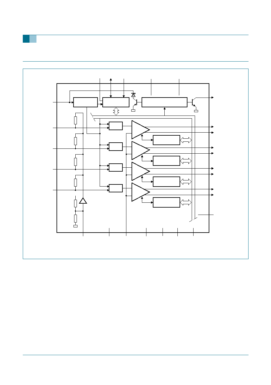
The TDA8595 is a complementary quad Bridge Tied Load (BTL) audio power amplifier
made in BCDMOS technology. It contains four independent amplifiers in BTL
configuration. Through the I
2
C-bus, diagnosis of temperature warning and clipping level is
fully programmable and the information available via two diagnostic pins is selectable. The
status of each amplifier (output offset, load or no load, short-circuit or speaker incorrectly
connected) can be read separately.
2.
Features
2.1 General
s
Operates in legacy mode (non I
2
C-bus) and I
2
C-bus mode (3.3 V and 5 V compliant)
s
Three hardware programmable I
2
C-bus addresses
s
Drive 4
or 2
loads
s
Speaker fault detection
s
Independent short-circuit protection per channel
s
Loss of ground and open V
P
safe (with 150 m
series impedance and a supply
decoupling capacitor of 2200
�
F maximum)
s
All outputs short-circuit proof to ground, supply voltage and across the load
s
All pins short-circuit proof to ground
s
Temperature-controlled gain reduction to prevent audio holes at high junction
temperatures
s
Low battery voltage detection
s
Offset detection
2.2 I
2
C-bus mode
s
DC load detection: open-circuit, short-circuit and load present
s
AC load (tweeter) detection
s
During start-up, can detect which load is connected so the appropriate gain can be
selected without audio plop
s
Independently selectable soft mute of front channels (channel 1 and channel 3) and
rear channels (channel 2 and channel 4)
s
Programmable gain (26 dB and 16 dB) of front channels and rear channels
s
Fully programmable diagnostic levels can be set:
x
Programmable clip detection: 2 %, 5 % or 10 %
x
Programmable thermal pre-warning
TDA8595
I
2
C-bus controlled 4
�
45 W power amplifier
Rev. 01 -- 20 April 2006
Product data sheet
9397 750 15067
� Koninklijke Philips Electronics N.V. 2006. All rights reserved.
Product data sheet
Rev. 01 -- 20 April 2006
2 of 49
Philips Semiconductors
TDA8595
I
2
C-bus controlled 4
�
45 W power amplifier
s
Selectable information on the DIAG and STB pins:
x
The STB pin can be programmed/multiplexed with second clip detection
x
Clip information of each channel can be directed separately to the DIAG pin or the
STB pin
x
Independent enabling of thermal, clip or load fault detection (short across or to V
P
or to ground) on DIAG pin
3.
Quick reference data
4.
Ordering information
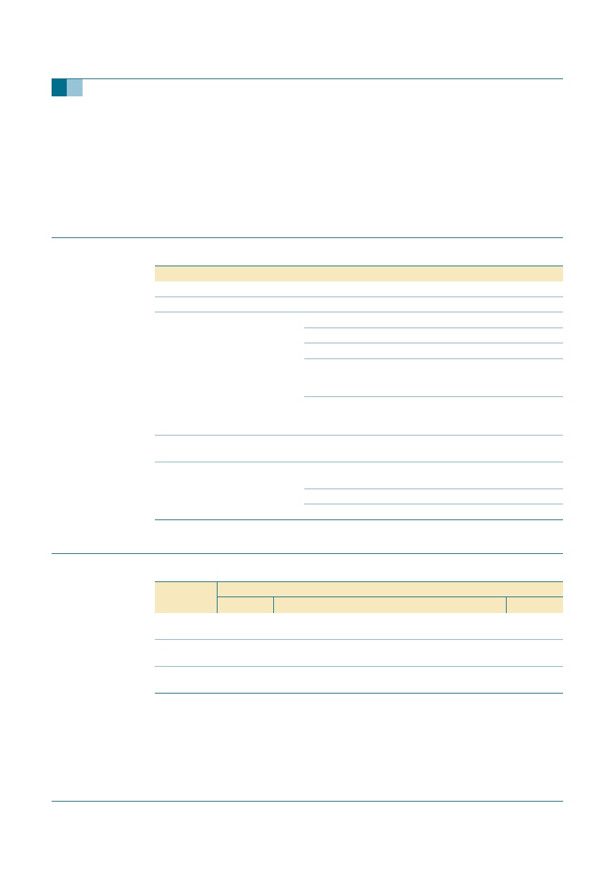
Table 1:
Quick reference data
Symbol
Parameter
Conditions
Min
Typ
Max
Unit
V
P
supply voltage
R
L
= 4
8
14.4
18
V
I
q
quiescent current
no load
-
270
400
mA
P
o
output power
V
P
= 14.4 V
R
L
= 4
; THD = 0.5 %
18
20
-
W
R
L
= 4
; THD = 10 %
23
25
-
W
R
L
= 4
; maximum
power; V
i
= 2 V (RMS)
square wave
37
40
-
W
R
L
= 2
; maximum
power; V
i
= 2 V (RMS)
square wave
58
64
-
W
THD
total harmonic
distortion
R
L
= 4
; f = 1 kHz;
P
o
= 1 W to 12 W
-
0.01
0.1
%
V
n(o)
noise output
voltage
filter 20 Hz to 22 kHz;
R
S
=1 k
normal mode
-
45
65
�
V
line driver mode
-
22
29
�
V
Table 2:
Ordering information
Type
number
Package
Name
Description
Version
TDA8595J
DBS27P
plastic DIL-bent-SIL (special bent) power package; 27
leads (lead length 6.8 mm)
SOT827-1
TDA8595TH
HSOP36
plastic, heatsink small outline package; 36 leads;
low stand-off height
SOT851-2
TDA8595SD
RDBS27P
plastic rectangular-DIL-bent-SIL (reverse bent) power
package; 27 leads (row spacing 2.54 mm)
SOT878-1
9397 750 15067
� Koninklijke Philips Electronics N.V. 2006. All rights reserved.
Product data sheet
Rev. 01 -- 20 April 2006
5 of 49
Philips Semiconductors
TDA8595
I
2
C-bus controlled 4
�
45 W power amplifier
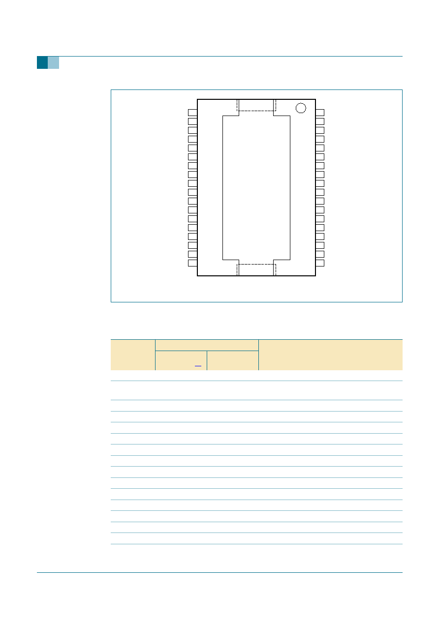
6.2 Pin description
Fig 3.
Pin configuration TDA8595TH
TDA8595TH
DIAG
n.c.
OUT2
-
OUT1
-
PGND2
PGND1
OUT2+
TAB
V
P2
V
P2
OUT1+
STB
SVR
ADSEL
IN1
n.c.
IN2
SDA
n.c.
OUT4+
SGND
n.c.
IN4
IN3
001aad138
36
35
34
33
32
31
30
29
28
27
26
25
11
12
9
10
7
8
ACGND
OUT3+
n.c.
V
P1
PGND3
24
23
22
21
15
16
13
14
V
P1
OUT3
-
n.c.
n.c.
20
19
17
18
5
6
3
4
1
2
PGND4
OUT4
-
SCL
Table 3:
Pin description
Symbol
Pin
Description
TDA8595J
TDA8595SD
[1]
TDA8595TH
ADSEL
1
28
I
2
C-bus address select
STB
2
29
standby (I
2
C-bus mode) or mode pin (legacy
mode); programmable second clip indicator
PGND2
3
31
power ground channel 2
OUT2
-
4
32
negative channel 2 output
DIAG
5
33
diagnostic/clip detection output
OUT2+
6
30
positive channel 2 output
V
P2
7
34 and 35
supply voltage 2
n.c.
-
1
not connected
OUT1
-
8
2
negative channel 1 output
PGND1
9
3
power ground channel 1
OUT1+
10
4
positive channel 1 output
SVR
11
5
half supply filter capacitor
IN1
12
6
channel 1 input
IN2
13
7
channel 2 input
n.c.
-
8
not connected
SGND
14
9
signal ground