 | –≠–ª–µ–∫—Ç—Ä–æ–Ω–Ω—ã–π –∫–æ–º–ø–æ–Ω–µ–Ω—Ç: TDA8708AT | –°–∫–∞—á–∞—Ç—å:  PDF PDF  ZIP ZIP |

DATA SHEET
Product specification
Supersedes data of April 1993
File under Integrated Circuits, IC02
June 1994
INTEGRATED CIRCUITS
Philips Semiconductors
TDA8708A
Video analog input interface

June 1994
2
Philips Semiconductors
Product specification
Video analog input interface
TDA8708A
FEATURES
∑
8-bit resolution
∑
Sampling rate up to 32 MHz
∑
Binary or two's complement 3-state TTL outputs
∑
TTL-compatible digital inputs and outputs
∑
Internal reference voltage regulator
∑
Power dissipation of 365 mW (typical)
∑
Input selector circuit (one out of three video inputs)
∑
Clamp and Automatic Gain Control (AGC) functions for
CVBS and Y signals
∑
No sample-and-hold circuit required.
∑
The TDA8708A has white peak control in modes 1 and
2 whereas the TDA8708B has control in mode 1 only.
APPLICATIONS
∑
Video signal decoding
∑
Scrambled TV (encoding and decoding)
∑
Digital picture processing
∑
Frame grabbing.
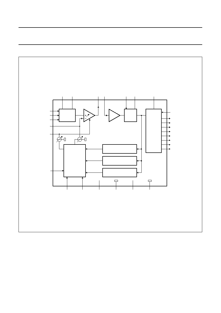
GENERAL DESCRIPTION
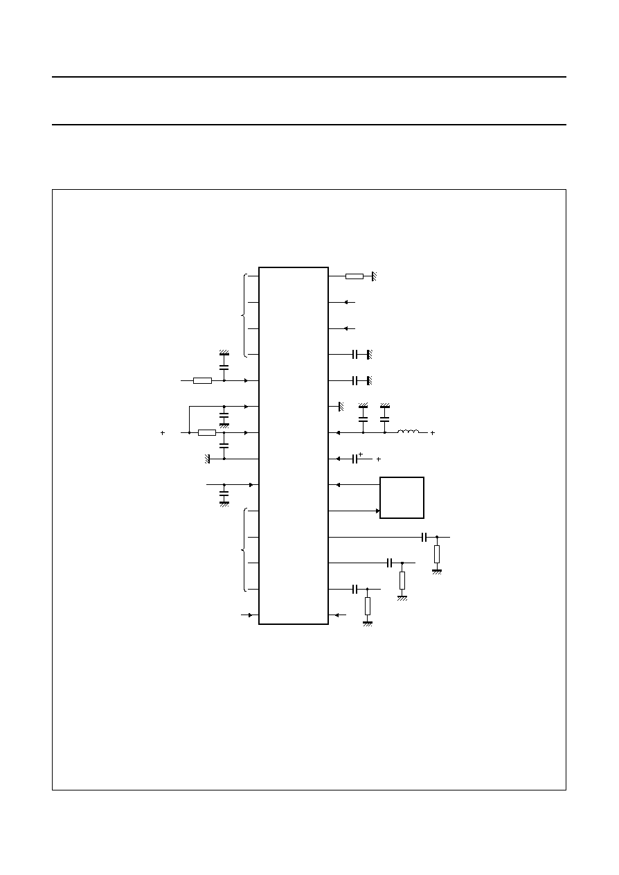
The TDA8708A is an analog input interface for video signal
processing. It includes a video amplifier with clamp and
gain control, an 8-bit analog-to-digital converter (ADC)
with a sampling rate of 32 MHz and an input selector.
QUICK REFERENCE DATA
ORDERING INFORMATION
SYMBOL
PARAMETER
MIN.
TYP.
MAX.
UNIT
V
CCA
analog supply voltage
4.5
5.0
5.5
V
V
CCD
digital supply voltage
4.5
5.0
5.5
V
V
CCO
TTL output supply voltage
4.2
5.0
5.5
V
I
CCA
analog supply current
-
37
45
mA
I
CCD
digital supply current
-
24
30
mA
I
CCO
TTL output supply current
-
12
16
mA
ILE
DC integral linearity error
-
-
±
1
LSB
DLE
DC differential linearity error
-
-
±
0.5
LSB
f
clk(max)
maximum clock frequency
30
32
-
MHz
B
maximum
-
3 dB bandwidth (AGC amplifier)
12
18
-
MHz
P
tot
total power dissipation
-
365
500
mW
TYPE NUMBER
PACKAGE
PINS
PIN POSITION
MATERIAL
CODE
TDA8708A
28
DIP
plastic
SOT117-1
TDA8708AT
28
SO28L
plastic
SOT136-1
June 1994
3
Philips Semiconductors
Product specification
Video analog input interface
TDA8708A
BLOCK DIAGRAM
Fig.1 Block diagram.
andbook, full pagewidth
MBB965
TTL
OUTPUTS
9
1
2
3
4
10
11
12
13
output format/
chip enable
(3-state input)
D7
D6
D5
D4
D3
D2
D1
D0
8 - bit
ADC
AMP.
VIDEO
AMPLIFIER
INPUT
SELECTOR
16
17
18
19
20
14
15
video input
selection bit 0
video input
selection bit 1
analog
voltage
output
ADC
input
clock
input
decoupling
input
5
21
7
TTL outputs
video input 0
video input 1
video input 2
clamp capacitor
connection
AGC capacitor
connection
24
25
AGC &
CLAMP
LOGIC
&
MODE
SELECTION
PEAK LEVEL
DIGITAL COMPARATOR
27
26
sync level
sync pulse
black level
sync pulse
6
digital VCCD
(+ 5 V)
digital
ground
8
22
analog VCCA
(+ 5 V)
VCCO (+ 5 V)
analog
ground
23
TDA8708A
28
BLACK LEVEL
DIGITAL COMPARATOR
SYNC LEVEL
DIGITAL COMPARATOR
peak level current
resistor input
June 1994
4
Philips Semiconductors
Product specification
Video analog input interface
TDA8708A
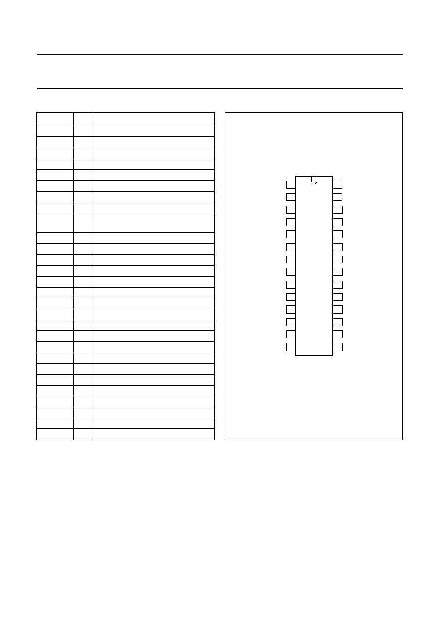
PINNING
SYMBOL
PIN
DESCRIPTION
D7
1
data output; bit 7 (MSB)
D6
2
data output; bit 6
D5
3
data output; bit 5
D4
4
data output; bit 4
CLK
5
clock input
V
CCD
6
digital supply voltage (+5 V)
V
CCO
7
TTL outputs supply voltage (+5 V)
DGND
8
digital ground
OF
9
output format/chip enable
(3-state input)
D3
10
data output; bit 3
D2
11
data output; bit 2
D1
12
data output; bit 1
D0
13
data output; bit 0 (LSB)
I0
14
video input selection bit 0
I1
15
video input selection bit 1
VIN0
16
video input 0
VIN1
17
video input 1
VIN2
18
video input 2
ANOUT
19
analog voltage output
ADCIN
20
analog-to-digital converter input
DEC
21
decoupling input
V
CCA
22
analog supply voltage (+5 V)
AGND
23
analog ground
CLAMP
24
clamp capacitor connection
AGC
25
AGC capacitor connection
GATE B
26
black level synchronization pulse
GATE A
27
sync level synchronization pulse
RPEAK
28
peak level current resistor input
Fig.2 Pin configuration.
1
2
3
4
5
6
7
8
9
10
11
12
13
28
27
26
25
24
23
22
21
20
19
18
17
16
15
14
TDA8708A
D7
D6
D5
D4
CLK
VCCD
VCCO
DGND
OF
D3
D2
D1
D0
I0
ADCIN
ANOUT
VIN2
VIN1
VIN0
I1
GATE B
AGC
CLAMP
AGND
VCCA
DEC
RPEAK
GATE A
MBB964

June 1994
5
Philips Semiconductors
Product specification
Video analog input interface
TDA8708A
FUNCTIONAL DESCRIPTION
The TDA8708A provides a simple interface for decoding
video signals.
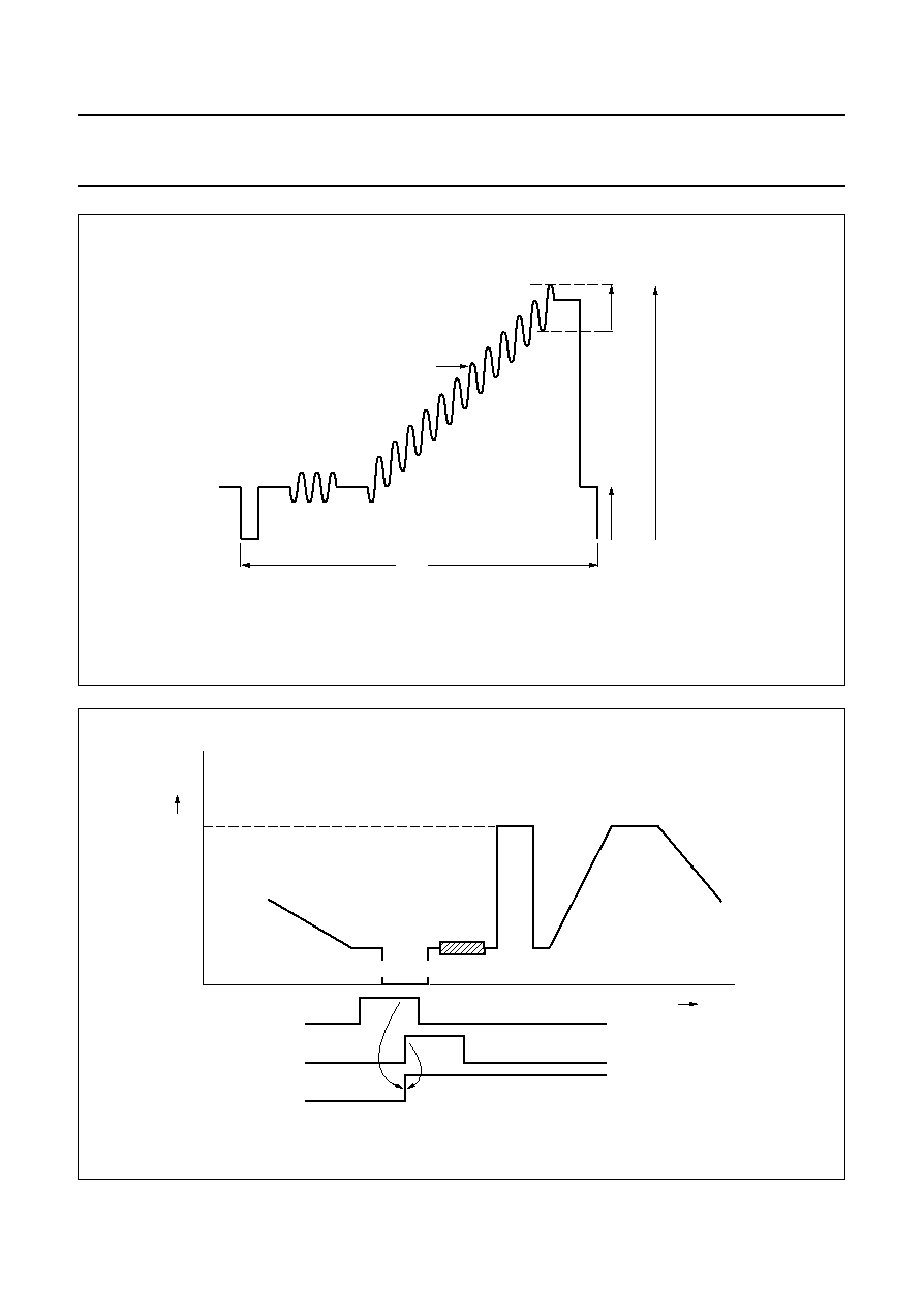
The TDA8708A operates in configuration mode 1 (see
Fig.4) when the video signals are weak (i.e. when the gain
of the AGC amplifier has not yet reached its optimum
value). This enables a fast recovery of the synchronization
pulses in the decoder circuit. When the pulses at the
GATE A and GATE B inputs become distinct (GATE A and
GATE B pulses are synchronization pulses occurring
during the sync period and rear porch respectively) the
TDA8708A automatically switches to configuration mode 2
(see Fig.5).
When the TDA8708A is in configuration mode 1, the gain
of the AGC amplifier will be roughly adjusted (sync level to
a digital output level of 0 and the peak level to a digital
output level of 255).
In configuration mode 2 the digital output of the ADC is
compared to internal digital reference levels. The resultant
outputs control the charge or discharge current of a
capacitor connected to the AGC pin. The voltage across
this capacitor controls the gain of the video amplifier. This
is the gain control loop.
The sync level comparator is active during a positive-going
pulse at the GATE A input. This means that the sync pulse
of the composite video signal is used as an amplitude
reference. The bottom of the sync pulse is adjusted to
obtain a digital output of logic 0 at the converter output. As
the black level is at digital level 64, the sync pulse will have
a digital amplitude of 64 LSBs.
The peak-white control loop is always active. If the video
signal tends to exceed the digital code of 248, the gain will
be limited to avoid any over-range of the converter.
The use of nominal signals will prevent the output from
exceeding a digital code of 213 and the peak-white control
loop will be non-active.
The clamp level control is accomplished by using the same
techniques as used for the gain control. The black-level
digital comparator is active during a positive-going pulse at
the GATE B input. The clamp capacitor will be charged or
discharged to adjust the digital output to code 64.
LIMITING VALUES
In accordance with the Absolute Maximum Rating System (IEC 134).
THERMAL CHARACTERISTICS
SYMBOL
PARAMETER
MIN.
MAX.
UNIT
V
CCA
analog supply voltage
-
0.3
+7.0
V
V
CCD
digital supply voltage
-
0.3
+7.0
V
V
CCO
output supply voltage
-
0.3
+7.0
V
V
CC
supply voltage difference between V
CCA
and V
CCD
-
1.0
+1.0
V
supply voltage difference between V
CCO
and V
CCD
-
1.0
+1.0
V
supply voltage difference between V
CCA
and V
CCO
-
1.0
+1.0
V
V
I
input voltage
-
0.3
V
CCA
V
I
O
output current
0
+10
mA
T
stg
storage temperature
-
55
+150
∞
C
T
amb
operating ambient temperature
0
+70
∞
C
T
j
junction temperature
0
+125
∞
C
SYMBOL
PARAMETER
VALUE
UNIT
R
th j-a
thermal resistance from junction to ambient in free air
SOT117-1
55
K/W
SOT136-1
70
K/W

June 1994
6
Philips Semiconductors
Product specification
Video analog input interface
TDA8708A
CHARACTERISTICS
V
CCA
= V
22
to V
23
= 4.5 to 5.5 V; V
CCD
= V
6
to V
8
= 4.5 to 5.5 V; V
CCO
= V
7
to V
8
= 4.2 to 5.5 V; AGND and DGND
shorted together; V
CCA
to V
CCD
=
-
0.5 to +0.5 V; V
CCO
to V
CCD
=
-
0.5 to +0.5 V; V
CCA
to V
CCO
=
-
0.5 to +0.5 V;
T
amb
= 0 to +70
∞
C; typical readings taken at V
CCA
= V
CCD
= V
CCO
= 5 V and T
amb
= 25
∞
C; unless otherwise specified.
SYMBOL
PARAMETER
CONDITIONS
MIN.
TYP.
MAX.
UNIT
Supplies
V
CCA
analog supply voltage
4.5
5.0
5.5
V
V
CCD
digital supply voltage
4.5
5.0
5.5
V
V
CCO
TTL output supply voltage
4.2
5.0
5.5
V
I
CCA
analog supply current
-
37
45
mA
I
CCD
digital supply current
-
24
30
mA
I
CCO
TTL output supply current
TTL load (see Fig.8)
-
12
16
mA
Video amplifier inputs
VIN(0
TO
2)
INPUTS
V
I(p-p)
input voltage (peak-to-peak value)
AGC load with external
capacitor; note 1
0.6
-
1.5
V
|
Z
i
|
input impedance
f
i
= 6 MHz
10
20
-
k
C
I
input capacitance
f
i
= 6 MHz
-
1
-
pF
I0
AND
I1 TTL
INPUTS
(
SEE TABLE
1)
V
IL
LOW level input voltage
0
-
0.8
V
V
IH
HIGH level input voltage
2.0
-
V
CCD
V
I
IL
LOW level input current
V
I
= 0.4 V
-
400
-
-
µ
A
I
IH
HIGH level input current
V
I
= 2.7 V
-
-
20
µ
A
GATE A
AND
GATE B TTL
INPUTS
(
SEE FIGS
4
AND
5)
V
IL
LOW level input voltage
0
-
0.8
V
V
IH
HIGH level input voltage
2.0
-
V
CCD
V
I
IL
LOW level input current
V
I
= 0.4 V
-
400
-
-
µ
A
I
IH
HIGH level input current
V
I
= 2.7 V
-
-
20
µ
A
t
W
pulse width
see Fig.5
2
-
-
µ
s
RPEAK
INPUT
(
PIN
28)
I
28(min)
minimum peak level current
R
28
= 0
-
80
150
µ
A
AGC
INPUT
(
PIN
25)
V
25(min)
AGC voltage for minimum gain
-
2.8
-
V
V
25(max)
AGC voltage for maximum gain
-
4.0
-
V
AGC output current
see Table 2
CLAMP
INPUT
(
PIN
24)
V
24
clamp voltage for code 128 output
-
3.5
-
V
I
24
clamp output current
see Table 3
June 1994
7
Philips Semiconductors
Product specification
Video analog input interface
TDA8708A
Video amplifier outputs
ANOUT
OUTPUT
(
PIN
19)
V
19(p-p)
AC output voltage
(peak-to-peak value)
V
VIN
= 1.33 V (p-p);
V
25
= 3.6 V
-
1.33
-
V
I
19
internal current source
R
L
=
2.0
2.5
-
mA
I
O(p-p)
output current driven by the load
V
ANOUT
= 1.33 V (p-p);
note 2
-
-
1.0
mA
V
19
DC output voltage for black level
note 3
-
V
CCA
-
2.24
-
V
Z
19
output impedance
-
20
-
Video amplifier dynamic characteristics
ct
crosstalk between VIN inputs
V
CCA
= 4.75 to 5.25 V
-
-
50
-
45
dB
G
diff
differential gain
V
VIN
= 1.33 V (p-p);
V
25
= 3.6 V
-
2
-
%
diff
differential phase
V
VIN
= 1.33 V (p-p);
V
25
= 3.6 V
-
0.8
-
deg
B
-
3 dB bandwidth
12
-
-
MHz
S/N
signal-to-noise ratio
note 4
60
-
-
dB
SVRR1
supply voltage ripple rejection
note 5
-
45
-
dB
G
gain range
see Fig.10
-
4.5
-
+6.0
dB
G
stab
gain stability as a function of supply
voltage and temperature
see Fig.10
-
-
5
%
Analog-to-digital converter inputs
CLK
INPUT
(
PIN
5)
V
IL
LOW level input voltage
0
-
0.8
V
V
IH
HIGH level input voltage
2.0
-
V
CCD
V
I
IL
LOW level input current
V
clk
= 0.4 V
-
400
-
-
µ
A
I
IH
HIGH level input current
V
clk
= 2.7 V
-
-
100
µ
A
|
Z
i
|
input impedance
f
clk
= 10 MHz
-
4
-
k
C
I
input capacitance
f
clk
= 10 MHz
-
4.5
-
pF
OF
INPUT
(3-
STATE
;
SEE TABLE
4)
V
IL
LOW level input voltage
0
-
0.2
V
V
IH
HIGH level input voltage
2.6
-
V
CCD
V
V
9
input voltage in high impedance state
-
1.15
-
V
I
IL
LOW level input current
-
370
-
300
-
µ
A
I
IH
HIGH level input current
-
300
450
µ
A
SYMBOL
PARAMETER
CONDITIONS
MIN.
TYP.
MAX.
UNIT

June 1994
8
Philips Semiconductors
Product specification
Video analog input interface
TDA8708A
ADCIN
INPUT
(
PIN
20;
SEE
T
ABLE
5)
V
20
input voltage
digital output = 00
-
V
CCA
-
2.42
-
V
V
20
input voltage
digital output = 255
-
V
CCA
-
1.41
-
V
V
20(p-p)
input voltage amplitude
(peak-to-peak value)
-
1.0
-
V
I
20
input current
-
1.0
10
µ
A
|
Z
i
|
input impedance
f
i
= 6 MHz
-
50
-
M
C
I
input capacitance
f
i
= 6 MHz
-
1
-
pF
Analog-to-digital converter outputs
D
IGITAL OUTPUTS
D0
TO
D7
V
OL
LOW level output voltage
I
OL
= 2 mA
0
-
0.6
V
V
OH
HIGH level output voltage
I
OL
=
-
0.4 mA
2.4
-
V
CCD
V
I
OZ
output current in 3-state mode
0.4 V < V
O
< V
CCD
-
20
-
+20
µ
A
Switching characteristics
f
clk(max)
maximum clock input frequency
see Fig.6; note 6
30
32
-
MHz
Analog signal processing (f
clk
= 32 MHz; see Fig.8)
G
diff
differential gain
V
20
= 1.0 V (p-p);
see Fig.3; note 7
-
2
-
%
diff
differential phase
see Fig.3; note 7
-
2
-
deg
f
1
fundamental harmonics (full-scale)
f
i
= 4.43 MHz; note 7
-
-
0
dB
f
all
harmonics (full-scale);
all components
f
i
= 4.43 MHz; note 7
-
-
55
-
dB
SVRR2
supply voltage ripple rejection
note 8
-
1
5
%/V
Transfer function (see Fig.8)
ILE
DC integral linearity error
-
-
±
1
LSB
DLE
DC differential linearity error
-
-
±
0.5
LSB
ILE
AC integral linearity error
note 9
-
-
±
2
LSB
Timing (f
clk
= 32 MHz; see Figs 6, 7 and 8)
D
IGITAL OUTPUTS
(C
L
= 15 pF; I
OL
= 2 mA; R
L
= 2 k
)
t
ds
sampling delay time
-
2
-
ns
t
h
output hold time
6
8
-
ns
t
d
output delay time
-
16
20
ns
t
dEZ
3-state delay time; output enable
-
19
25
ns
t
dDZ
3-state delay time; output disable
-
14
20
ns
SYMBOL
PARAMETER
CONDITIONS
MIN.
TYP.
MAX.
UNIT

June 1994
9
Philips Semiconductors
Product specification
Video analog input interface
TDA8708A
Notes
1. 0 dB is obtained at the AGC amplifier when applying V
i(p-p)
= 1.33 V.
2. The output current at pin 19 should not exceed 1 mA. The load impedance R
L
should be referenced to V
CCA
and
defined as:
a) AC impedance
1 k
and the DC impedance >2.7 k
.
b) The load impedance should be coupled directly to the output of the amplifier so that the DC voltage supplied by
the clamp is not disturbed.
3. Control mode 2 is selected.
4. Signal-to-noise ratio measured with 5 MHz bandwidth:
5. The voltage ratio is expressed as:
for V
I
= 1 V (p-p), gain at 100 kHz = 1 and 1 V supply variation.
6. It is recommended that the rise and fall times of the clock are
2 ns. In addition, a `good layout' for the digital and
analog grounds is recommended.
7. These measurements are realized on analog signals after a digital-to-analog conversion (TDA8702 is used).
8. The supply voltage rejection is the relative variation of the analog signal (full-scale signal at input) for 1 V of supply
variation:
9. Full-scale sine wave (f
i
= 4.4 MHz; f
clk
= 27 MHz).
S
N
----
20 log
V
ANOUTC p
p
≠
(
)
V
ANOUTY (RMS noise)
-------------------------------------------------at B = 5 MHz.
=
SVRR1
20 log
V
CCA
V
CCA
------------------
G
G
--------
◊
=
SVRR2
V
I 00
( )
V
I FF
(
)
≠
(
)
V
I 00
( )
V
I FF
(
)
≠
(
)
+
V
CCA
-----------------------------------------------------------------------------------------------------
=
June 1994
10
Philips Semiconductors
Product specification
Video analog input interface
TDA8708A
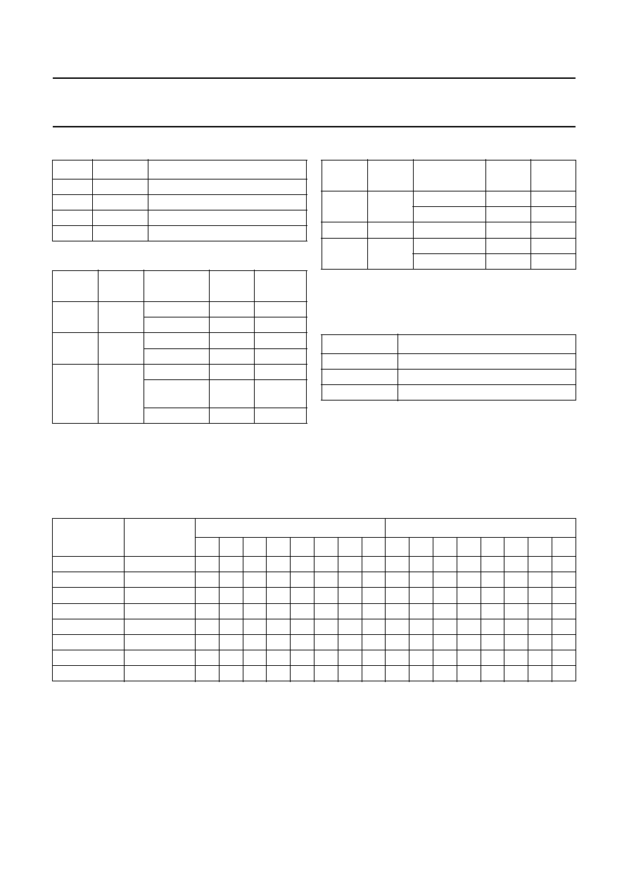
Table 1 Video input selection (CVBS).
Table 2 AGC output current.
Note
1. X = don't care.
2. Mode 2 can only be initialized with successive pulses
on GATE A and GATE B (see Fig.5).
I1
I0
SELECTED INPUT
0
0
VIN0
0
1
VIN1
1
0
VIN2
1
1
VIN2
GATE A GATE B
DIGITAL
OUTPUT
I
AGC
MODE
(2)
1
1
output
<
255
-
2.5
µ
A
1
output
>
255
I
AGCM
1
0
X
(1)
output
<
248
0
µ
A
2
output
>
248
I
AGCM
2
1
0
output
<
0
+2.5
µ
A
2
0 < output <
248
-
2.5
µ
A
2
output > 248
I
AGCM
2
Table 3 CLAMP output current.
Note
1. X = don't care.
Table 4 OF input coding.
Note
1. Use C
10 pF to DGND.
GATE A GATE B
DIGITAL
OUTPUT
I
CLAMP
MODE
1
1
output
<
0
I
CLAMPM
1
output
>
0
-
2.5
µ
A
1
X
(1)
0
X
(1)
0
µ
A
2
0
1
output
<
64
+50
µ
A
2
64 < output
-
50
µ
A
2
OF
D0 TO D7
0
active, two's complement
1
high impedance
open circuit
(1)
active, binary
Table 5 Output coding and input voltage (typical values).
STEP
V
ADCIN
BINARY OUTPUTS
TWO'S COMPLEMENT
D7
D6
D5
D4
D3
D2
D1
D0
D7
D6
D5
D4
D3
D2
D1
D0
Underflow
-
0
0
0
0
0
0
0
0
1
0
0
0
0
0
0
0
0
V
CCA
-
2.41 V
0
0
0
0
0
0
0
0
1
0
0
0
0
0
0
0
1
-
0
0
0
0
0
0
0
1
1
0
0
0
0
0
0
1
.
-
.
.
.
.
.
.
.
.
.
.
.
.
.
.
.
.
.
-
.
.
.
.
.
.
.
.
.
.
.
.
.
.
.
.
254
-
1
1
1
1
1
1
1
0
0
1
1
1
1
1
1
0
255
V
CCA
-
1.41 V
1
1
1
1
1
1
1
1
0
1
1
1
1
1
1
1
Overflow
-
1
1
1
1
1
1
1
1
0
1
1
1
1
1
1
1
June 1994
11
Philips Semiconductors
Product specification
Video analog input interface
TDA8708A
Fig.3 Test signal on the ADCIN pin for differential gain and phase measurements.
handbook, full pagewidth
MBB959
64
µ
s
0.25 V
1.0 V
0.25 V
5 MHz sine wave
Fig.4 Control mode 1.
ndbook, full pagewidth
MBB969
digital
output
level
255
0
time
black-level
clamping
GATE A
GATE B
MODE 1
peak-level gain control
sync-level gain control
June 1994
12
Philips Semiconductors
Product specification
Video analog input interface
TDA8708A
Fig.5 Control mode 2.
handbook, full pagewidth
MBB970
digital
output
level
64
248
0
time
black-level
clamping
213
safety
margin
standard picture
level
GATE A
GATE B
MODE 2
sync-level control
peak-level gain control
t W
t W
Fig.6 Timing diagram for data output.
handbook, full pagewidth
MBB958
data N 1
data N
data N 2
data N 3
2.4 V
0.4 V
t d
data N 1
clock input
reference level
(1.5 V)
CLK
input
analog
input
(ADCIN)
data
outputs
D0 to D7)
t h
t
ds
sample
N 1
sample
N
sample
N 1
sample
N 2

June 1994
13
Philips Semiconductors
Product specification
Video analog input interface
TDA8708A
Fig.7 Output format timing diagram.
handbook, full pagewidth
MBB968
OF
input
data
outputs
(D0 to D7)
2.4 V
0.4 V
dEZ
t
dDZ
t
high impedance
open
two's complement
binary
Fig.8 Load circuit for timing measurement; data outputs (OF = LOW or open-circuit).
handbook, halfpage
MBD865
D0 to D7
15 pF
2 k
VCCO
DGND
IN916
or
IN3064
June 1994
14
Philips Semiconductors
Product specification
Video analog input interface
TDA8708A
Fig.9 Load circuit for timing measurement; 3-state outputs (OF: f
i
= 1 MHz; V
OF
= 3 V).
handbook, halfpage
MBB955
D0 to D7
C
5
k
S1
2 k
VCCO
S2
DGND
IN916
or
IN3064
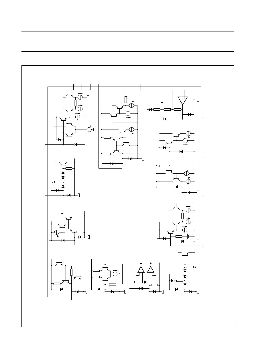
Fig.10 Gain control curve.
(1) Typical value (V
CCA
= V
CCD
= 5 V; T
amb
= 25
∞
C).
(2) Minimum and maximum values (temperature and supply).
2.6
4.6
12
8
4
MSA676
0
4
8
3
3.4
3.8
4.2
G
(dB)
V (V)
25
5 %
(1)
(2)
June 1994
15
Philips Semiconductors
Product specification
Video analog input interface
TDA8708A
INTERNAL PIN CIRCUITRY
handbook, full pagewidth
MBB971
20
k
AGND
V
CCA
AGND
V
CCA
AGND
V
CCA
2.5
mA
AGND
V
CCA
AGND
V
bottom
REF
V
CCA
V
V
mid
V
top
DGND
V
CCD
pins 16 to 18
VIN0, VIN1 and VIN2
DGND
V
CCO
AGND
V
CCA
pins 26 or 27
GATE A or GATE B
DGND
V
CCD
pin 25
AGC
V
CCA
1I
1I
0
1
2I
AGND
pin 21
DEC
pin 20
ADCIN
pin 19
ANOUT
pins 14 and 15
I , I
pin 9
OF
pin 5
clock input
pins 1 to 4
and 10 to 13
data outputs
pin 24
CLAMP
pin 22
V
CCA
pin 7
V
CCO
pin 6
V
CCD
pin 23
AGND
pin 8
DGND
TDA8708A
1.5 V
V
CCD
4 V
BE
V
REF
DGND
chip enable
binary/
two's complement
DGND
V
CCD
DGND
I
RPEAK
V
CCD
pin 28
RPEAK
Fig.11 Internal pin configuration.
June 1994
16
Philips Semiconductors
Product specification
Video analog input interface
TDA8708A
APPLICATION INFORMATION
Additional information can be found in the laboratory report
"FBL/AN9308".
Fig.12 Application diagram.
(1) It is recommended to decouple V
CCO
through a 22
resistor especially when
the output data of TDA8708A interfaces with a capacitive CMOS load device.
(2) See Figs 13 and 15 for examples of the low-pass filters.
handbook, full pagewidth
MBB967 - 1
TDA8708A
14
13
12
11
10
9
8
7
6
5
4
3
2
1
15
16
17
18
19
20
21
22
23
24
25
26
27
28
data outputs
33 pF
100
clock
22
(1)
22 nF
22 nF
5 V
data outputs
4.7
µ
F
4.7
µ
F
4.7
µ
F
75
5 V
10 nF
LOW PASS
FILTER
(2)
1
µ
H
220 nF
18 nF
horizontal clamp
10 pF
330
horizontal sync
1
µ
F
1
µ
F
75
75
5 V
June 1994
17
Philips Semiconductors
Product specification
Video analog input interface
TDA8708A
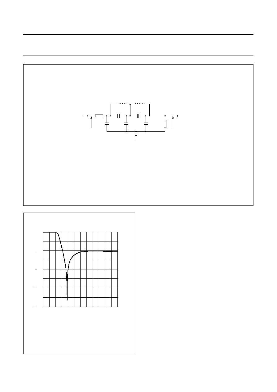
Fig.13 Example of a low-pass filter for CVBS and Y signals.
This filter can be adapted to various applications with respect to performance requirements. An input and output impedance of at least 680
and 2.2 k
must in any event be applied.
dbook, full pagewidth
MBB966 - 1
27 pF
68 pF
27 pF
2.2 k
12 pF
12 pF
22
µ
H
ANOUT
(pin 19)
ADCIN
(pin 20)
Vo
V i
VCCA
(pin 22)
680
22
µ
H
Fig.14 Frequency response for filter shown in
Fig.13.
handbook, halfpage
0
10
30
0
40
120
160
80
MSA682
20
f (MHz)
(dB)
Characteristics of Fig. 13
∑
Order 5; adapted CHEBYSHEV
∑
Ripple
0.4 dB
∑
f = 6.5 MHz at
-
3 dB
∑
f
notch
= 9.75 MHz.
June 1994
18
Philips Semiconductors
Product specification
Video analog input interface
TDA8708A
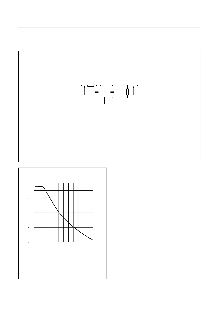
Fig.15 Example of an economical low-pass filter for CVBS and Y signals.
This filter can be adapted to various applications with respect to performance requirements. An input and output impedance of at least 680
and 2.2 k
must in any event be applied.
handbook, full pagewidth
MSA678
15 pF
15 pF
2.2 k
82
µ
H
ADOUT
(pin 19)
ADCIN
(pin 20)
VCCA
(pin 22)
680
Vo
V i
Fig.16 Frequency response for filter shown in Fig.15.
handbook, halfpage
0
10
30
0
10
30
40
20
MSA681
20
f (MHz)
(dB)
Characteristics of Fig. 15
∑
Order 5; adapted CHEBYSHEV
∑
Ripple
0.4 dB
∑
f = 6.5 MHz at
-
3 dB.
June 1994
19
Philips Semiconductors
Product specification
Video analog input interface
TDA8708A
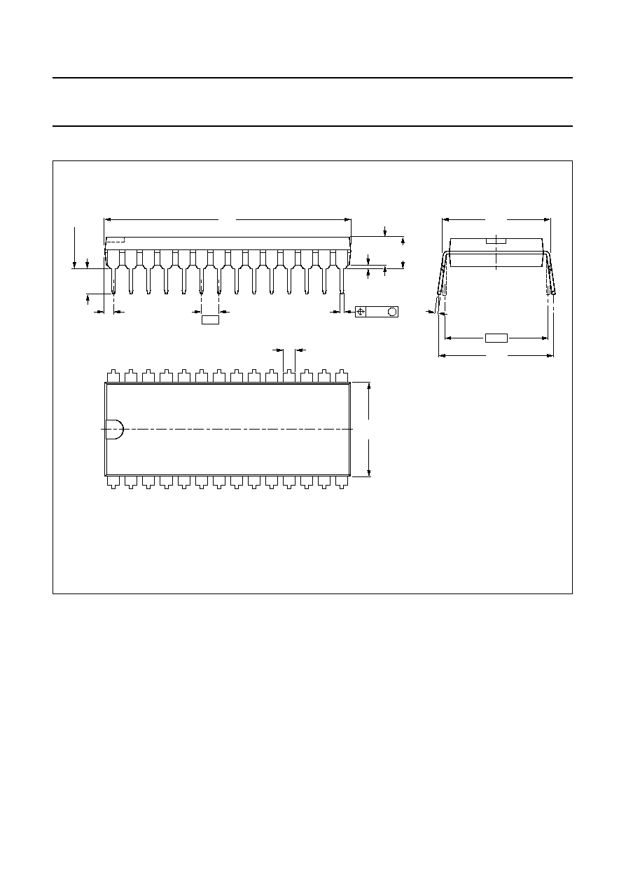
PACKAGE OUTLINES
Fig.17 Plastic dual in-line package; 28 leads (600 mil) with internal heat spreader (SOT117-1).
Dimensions in mm.
handbook, full pagewidth
28
1
15
14
1.7 max
14.1
13.7
36.0
35.0
4.0
max
5.1
max
0.51
min
3.9
3.4
seating plane
0.254
M
0.53
max
2.54
(13x)
1.7
max
15.80
15.24
0.32 max
15.24
17.15
15.90
MSA264

June 1994
20
Philips Semiconductors
Product specification
Video analog input interface
TDA8708A
Fig.18 Plastic small outline package; 28 leads; large body (SOT136-1).
Dimensions in mm.
handbook, full pagewidth
7.6
7.4
10.65
10.00
A
MBC236 - 1
0.3
0.1
2.45
2.25
1.1
0.5
0.32
0.23
1.1
1.0
0 to 8
o
2.65
2.35
detail A
S
18.1
17.7
0.1 S
1
14
15
28
pin 1
index
0.9
0.4
(4x)
0.25 M
(28x)
0.49
0.36
1.27

June 1994
21
Philips Semiconductors
Product specification
Video analog input interface
TDA8708A
SOLDERING
Plastic dual in-line packages
B
Y DIP OR WAVE
The maximum permissible temperature of the solder is
260
∞
C; this temperature must not be in contact with the
joint for more than 5 s. The total contact time of successive
solder waves must not exceed 5 s.
The device may be mounted up to the seating plane, but
the temperature of the plastic body must not exceed the
specified storage maximum. If the printed-circuit board has
been pre-heated, forced cooling may be necessary
immediately after soldering to keep the temperature within
the permissible limit.
R
EPAIRING SOLDERED JOINTS
Apply a low voltage soldering iron below the seating plane
(or not more than 2 mm above it). If its temperature is
below 300
∞
C, it must not be in contact for more than 10 s;
if between 300 and 400
∞
C, for not more than 5 s.
Plastic small-outline packages
B
Y WAVE
During placement and before soldering, the component
must be fixed with a droplet of adhesive. After curing the
adhesive, the component can be soldered. The adhesive
can be applied by screen printing, pin transfer or syringe
dispensing.
Maximum permissible solder temperature is 260
∞
C, and
maximum duration of package immersion in solder bath is
10 s, if allowed to cool to less than 150
∞
C within 6 s.
Typical dwell time is 4 s at 250
∞
C.
A modified wave soldering technique is recommended
using two solder waves (dual-wave), in which a turbulent
wave with high upward pressure is followed by a smooth
laminar wave. Using a mildly-activated flux eliminates the
need for removal of corrosive residues in most
applications.
B
Y SOLDER PASTE REFLOW
Reflow soldering requires the solder paste (a suspension
of fine solder particles, flux and binding agent) to be
applied to the substrate by screen printing, stencilling or
pressure-syringe dispensing before device placement.
Several techniques exist for reflowing; for example,
thermal conduction by heated belt, infrared, and
vapour-phase reflow. Dwell times vary between 50 and
300 s according to method. Typical reflow temperatures
range from 215 to 250
∞
C.
Preheating is necessary to dry the paste and evaporate
the binding agent. Preheating duration: 45 min at 45
∞
C.
R
EPAIRING SOLDERED JOINTS
(
BY HAND
-
HELD SOLDERING
IRON OR PULSE
-
HEATED SOLDER TOOL
)
Fix the component by first soldering two, diagonally
opposite, end pins. Apply the heating tool to the flat part of
the pin only. Contact time must be limited to 10 s at up to
300
∞
C. When using proper tools, all other pins can be
soldered in one operation within 2 to 5 s at between 270
and 320
∞
C. (Pulse-heated soldering is not recommended
for SO packages.)
For pulse-heated solder tool (resistance) soldering of VSO
packages, solder is applied to the substrate by dipping or
by an extra thick tin/lead plating before package
placement.

June 1994
22
Philips Semiconductors
Product specification
Video analog input interface
TDA8708A
DEFINITIONS
LIFE SUPPORT APPLICATIONS
These products are not designed for use in life support appliances, devices, or systems where malfunction of these
products can reasonably be expected to result in personal injury. Philips customers using or selling these products for
use in such applications do so at their own risk and agree to fully indemnify Philips for any damages resulting from such
improper use or sale.
Data sheet status
Objective specification
This data sheet contains target or goal specifications for product development.
Preliminary specification
This data sheet contains preliminary data; supplementary data may be published later.
Product specification
This data sheet contains final product specifications.
Limiting values
Limiting values given are in accordance with the Absolute Maximum Rating System (IEC 134). Stress above one or
more of the limiting values may cause permanent damage to the device. These are stress ratings only and operation
of the device at these or at any other conditions above those given in the Characteristics sections of the specification
is not implied. Exposure to limiting values for extended periods may affect device reliability.
Application information
Where application information is given, it is advisory and does not form part of the specification.

June 1994
23
Philips Semiconductors
Product specification
Video analog input interface
TDA8708A
NOTES

Philips Semiconductors
Philips Semiconductors ≠ a worldwide company
Argentina: IEROD, Av. Juramento 1992 - 14.b, (1428)
BUENOS AIRES, Tel. (541)786 7633, Fax. (541)786 9367
Australia: 34 Waterloo Road, NORTH RYDE, NSW 2113,
Tel. (02)805 4455, Fax. (02)805 4466
Austria: Triester Str. 64, A-1101 WIEN, P.O. Box 213,
Tel. (01)60 101-1236, Fax. (01)60 101-1211
Belgium: Postbus 90050, 5600 PB EINDHOVEN, The Netherlands,
Tel. (31)40 783 749, Fax. (31)40 788 399
Brazil: Rua do Rocio 220 - 5
th
floor, Suite 51,
CEP: 04552-903-S√O PAULO-SP, Brazil.
P.O. Box 7383 (01064-970).
Tel. (011)821-2327, Fax. (011)829-1849
Canada: INTEGRATED CIRCUITS:
Tel. (800)234-7381, Fax. (708)296-8556
DISCRETE SEMICONDUCTORS: 601 Milner Ave,
SCARBOROUGH, ONTARIO, M1B 1M8,
Tel. (0416)292 5161 ext. 2336, Fax. (0416)292 4477
Chile: Av. Santa Maria 0760, SANTIAGO,
Tel. (02)773 816, Fax. (02)777 6730
Colombia: IPRELENSO LTDA, Carrera 21 No. 56-17,
77621 BOGOTA, Tel. (571)249 7624/(571)217 4609,
Fax. (571)217 4549
Denmark: Prags Boulevard 80, PB 1919, DK-2300 COPENHAGEN S,
Tel. (032)88 2636, Fax. (031)57 1949
Finland: Sinikalliontie 3, FIN-02630 ESPOO,
Tel. (9)0-50261, Fax. (9)0-520971
France: 4 Rue du Port-aux-Vins, BP317,
92156 SURESNES Cedex,
Tel. (01)4099 6161, Fax. (01)4099 6427
Germany: PHILIPS COMPONENTS UB der Philips G.m.b.H.,
P.O. Box 10 63 23, 20043 HAMBURG,
Tel. (040)3296-0, Fax. (040)3296 213.
Greece: No. 15, 25th March Street, GR 17778 TAVROS,
Tel. (01)4894 339/4894 911, Fax. (01)4814 240
Hong Kong: PHILIPS HONG KONG Ltd., Components Div.,
6/F Philips Ind. Bldg., 24-28 Kung Yip St., KWAI CHUNG, N.T.,
Tel. (852)424 5121, Fax. (852)428 6729
India: Philips INDIA Ltd, Components Dept,
Shivsagar Estate, A Block ,
Dr. Annie Besant Rd. Worli, Bombay 400 018
Tel. (022)4938 541, Fax. (022)4938 722
Indonesia: Philips House, Jalan H.R. Rasuna Said Kav. 3-4,
P.O. Box 4252, JAKARTA 12950,
Tel. (021)5201 122, Fax. (021)5205 189
Ireland: Newstead, Clonskeagh, DUBLIN 14,
Tel. (01)640 000, Fax. (01)640 200
Italy: PHILIPS COMPONENTS S.r.l.,
Viale F. Testi, 327, 20162 MILANO,
Tel. (02)6752.3302, Fax. (02)6752 3300.
Japan: Philips Bldg 13-37, Kohnan 2 -chome, Minato-ku, TOKYO 108,
Tel. (03)3740 5028, Fax. (03)3740 0580
Korea: (Republic of) Philips House, 260-199 Itaewon-dong,
Yongsan-ku, SEOUL, Tel. (02)794-5011, Fax. (02)798-8022
Malaysia: No. 76 Jalan Universiti, 46200 PETALING JAYA,
SELANGOR, Tel. (03)750 5214, Fax. (03)757 4880
Mexico: Philips Components, 5900 Gateway East, Suite 200,
EL PASO, TX 79905, Tel. 9-5(800)234-7381, Fax. (708)296-8556
Netherlands: Postbus 90050, 5600 PB EINDHOVEN, Bldg. VB
Tel. (040)783749, Fax. (040)788399
New Zealand: 2 Wagener Place, C.P.O. Box 1041, AUCKLAND,
Tel. (09)849-4160, Fax. (09)849-7811
Norway: Box 1, Manglerud 0612, OSLO,
Tel. (022)74 8000, Fax. (022)74 8341
Pakistan: Philips Electrical Industries of Pakistan Ltd.,
Exchange Bldg. ST-2/A, Block 9, KDA Scheme 5, Clifton,
KARACHI 75600, Tel. (021)587 4641-49,
Fax. (021)577035/5874546.
Philippines: PHILIPS SEMICONDUCTORS PHILIPPINES Inc,
106 Valero St. Salcedo Village, P.O. Box 2108 MCC, MAKATI,
Metro MANILA, Tel. (02)810 0161, Fax. (02)817 3474
Portugal: PHILIPS PORTUGUESA, S.A.,
Rua dr. AntÛnio Loureiro Borges 5, Arquiparque - Miraflores,
Apartado 300, 2795 LINDA-A-VELHA,
Tel. (01)14163160/4163333, Fax. (01)14163174/4163366.
Singapore: Lorong 1, Toa Payoh, SINGAPORE 1231,
Tel. (65)350 2000, Fax. (65)251 6500
South Africa: S.A. PHILIPS Pty Ltd., Components Division,
195-215 Main Road Martindale, 2092 JOHANNESBURG,
P.O. Box 7430 Johannesburg 2000,
Tel. (011)470-5911, Fax. (011)470-5494.
Spain: Balmes 22, 08007 BARCELONA,
Tel. (03)301 6312, Fax. (03)301 42 43
Sweden: Kottbygatan 7, Akalla. S-164 85 STOCKHOLM,
Tel. (0)8-632 2000, Fax. (0)8-632 2745
Switzerland: Allmendstrasse 140, CH-8027 ZÐRICH,
Tel. (01)488 2211, Fax. (01)481 77 30
Taiwan: PHILIPS TAIWAN Ltd., 23-30F, 66, Chung Hsiao West
Road, Sec. 1. Taipeh, Taiwan ROC, P.O. Box 22978,
TAIPEI 100, Tel. (02)388 7666, Fax. (02)382 4382.
Thailand: PHILIPS ELECTRONICS (THAILAND) Ltd.,
209/2 Sanpavuth-Bangna Road Prakanong,
Bangkok 10260, THAILAND,
Tel. (662)398-0141, Fax. (662)398-3319.
Turkey: Talatpasa Cad. No. 5, 80640 GÐLTEPE/ISTANBUL,
Tel. (0 212)279 2770, Fax. (0212)269 3094
United Kingdom: Philips Semiconductors Limited, P.O. Box 65,
Philips House, Torrington Place, LONDON, WC1E 7HD,
Tel. (071)436 41 44, Fax. (071)323 03 42
United States: INTEGRATED CIRCUITS:
811 East Arques Avenue, SUNNYVALE, CA 94088-3409,
Tel. (800)234-7381, Fax. (708)296-8556
DISCRETE SEMICONDUCTORS: 2001 West Blue Heron Blvd.,
P.O. Box 10330, RIVIERA BEACH, FLORIDA 33404,
Tel. (800)447-3762 and (407)881-3200, Fax. (407)881-3300
Uruguay: Coronel Mora 433, MONTEVIDEO,
Tel. (02)70-4044, Fax. (02)92 0601
For all other countries apply to: Philips Semiconductors,
International Marketing and Sales, Building BAF-1,
P.O. Box 218, 5600 MD, EINDHOVEN, The Netherlands,
Telex 35000 phtcnl, Fax. +31-40-724825
SCD31
© Philips Electronics N.V. 1994
All rights are reserved. Reproduction in whole or in part is prohibited without the
prior written consent of the copyright owner.
The information presented in this document does not form part of any quotation
or contract, is believed to be accurate and reliable and may be changed without
notice. No liability will be accepted by the publisher for any consequence of its
use. Publication thereof does not convey nor imply any license under patent- or
other industrial or intellectual property rights.
Printed in The Netherlands
533061/1500/05/pp24
Date of release: June 1994
Document order number:
9397 734 20011