Document Outline
- FEATURES
- APPLICATIONS
- GENERAL DESCRIPTION
- QUICK REFERENCE DATA
- ORDERING INFORMATION
- BLOCK DIAGRAM
- PINNING
- LIMITING VALUES
- HANDLING
- THERMAL CHARACTERISTICS
- CHARACTERISTICS
- INTERNAL PIN CONFIGURATIONS
- APPLICATION INFORMATION
- PACKAGE OUTLINES
- SOLDERING
- DEFINITIONS
- LIFE SUPPORT APPLICATIONS

DATA SHEET
Product specification
Supersedes data of 1996 Jan 31
File under Integrated Circuits, IC02
1997 Oct 29
INTEGRATED CIRCUITS
TDA8714
8-bit high-speed analog-to-digital
converter

1997 Oct 29
2
Philips Semiconductors
Product specification
8-bit high-speed analog-to-digital converter
TDA8714
FEATURES
∑
8-bit resolution
∑
Sampling rate up to 80 MHz
∑
No missing codes guaranteed
∑
High signal-to-noise ratio over a large analog input
frequency range (7.7 effective bits at 4.43 MHz
full-scale input at f
clk
= 80 MHz)
∑
Overflow/underflow 3-state TTL output
∑
TTL compatible digital inputs
∑
Low-level AC clock input signal allowed
∑
External reference voltage regulator
∑
Power dissipation only 340 mW (typical)
∑
Low analog input capacitance, no buffer amplifier
required
∑
No sample-and-hold circuit required.
APPLICATIONS
High-speed analog-to-digital conversion for:
∑
video data digitizing
∑
radar pulse analysis
∑
transient signal analysis
∑
high energy physics research
∑
modulators
∑
medical imaging.
GENERAL DESCRIPTION
The TDA8714 is an 8-bit high-speed Analog-to-Digital
Converter (ADC) for professional video and other
applications. It converts the analog input signal into 8-bit
binary-coded digital words at a maximum sampling rate of
80 MHz. All digital inputs and outputs are TTL compatible,
although a low-level sine wave clock input signal is
allowed.
QUICK REFERENCE DATA
Note
1. Full-scale sine wave (f
i
= 4.43 MHz; f
clk
= 80 MHz).
SYMBOL
PARAMETER
CONDITIONS
MIN.
TYP.
MAX.
UNIT
V
CCA
analog supply voltage
4.75
5.0
5.25
V
V
CCD
digital supply voltage
4.75
5.0
5.25
V
V
CCO
output stages supply voltage
4.75
5.0
5.25
V
I
CCA
analog supply current
-
25
30
mA
I
CCD
digital supply current
-
27
33
mA
I
CCO
output stages supply current
-
16
20
mA
INL
DC integral non-linearity
-
±
0.4
±
0.5
LSB
DNL
DC differential non-linearity
-
±
0.2
±
0.35
LSB
AINL
AC integral non-linearity
note 1
-
±
0.5
±
1.0
LSB
f
clk(max)
maximum clock frequency
TDA8714/7
80
-
-
MHz
TDA8714/6
60
-
-
MHz
TDA8714/4
40
-
-
MHz
P
tot
total power dissipation
-
340
435
mW

1997 Oct 29
3
Philips Semiconductors
Product specification
8-bit high-speed analog-to-digital converter
TDA8714
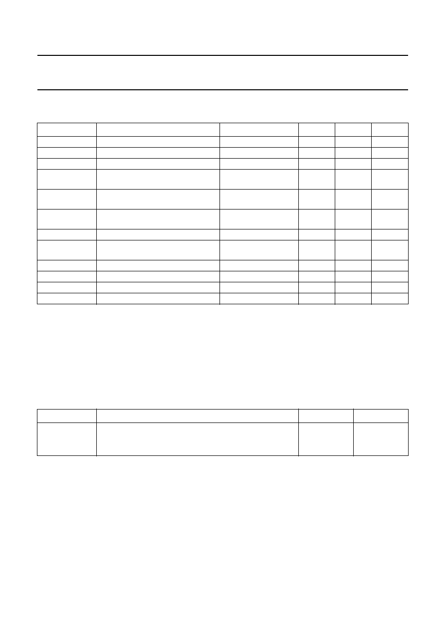
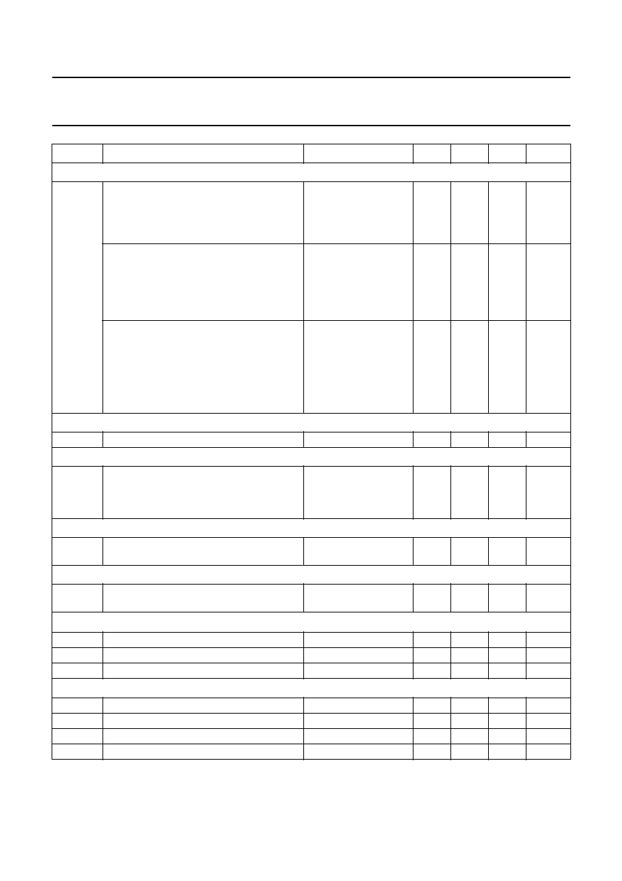
ORDERING INFORMATION
BLOCK DIAGRAM
TYPE
NUMBER
PACKAGE
SAMPLING
FREQUENCY (MHz)
NAME
DESCRIPTION
VERSION
TDA8714T/4
SO24
plastic small outline package; 24 leads;
body width 7.5 mm
SOT137-1
40
TDA8714T/6
SO24
SOT137-1
60
TDA8714T/7
SO24
SOT137-1
80
TDA8714M/4
SSOP24
plastic shrink small outline package; 24 leads;
body width 5.3 mm
SOT340-1
40
TDA8714M/6
SSOP24
SOT340-1
60
TDA8714M/7
SSOP24
SOT340-1
80
Fig.1 Block diagram.
handbook, full pagewidth
17
DGND
6
4
8
9
AGND
VRB
VRT
V I
18
VCCD
7
11
VCCA
23
15
14
13
24 D2
D3
D4
D5
D6
1
2
12
D1
D0
D7
OVERFLOW / UNDERFLOW
LATCH
TTL OUTPUTS
LATCHES
ANALOG -TO-DIGITAL
CONVERTER
CLOCK DRIVER
MSA669
TTL OUTPUT
16
CLK
22
CE
TDA8714
19
VCCO1
analog ground
digital ground
analog
voltage input
overflow / underflow
output
data outputs
LSB
MSB
21 VCCO2
output ground
20
OGND
1997 Oct 29
4
Philips Semiconductors
Product specification
8-bit high-speed analog-to-digital converter
TDA8714
PINNING
SYMBOL
PIN
DESCRIPTION
D1
1
data output; bit 1
D0
2
data output; bit 0 (LSB)
n.c.
3
not connected
V
RB
4
reference voltage BOTTOM input
n.c.
5
not connected
AGND
6
analog ground
V
CCA
7
analog supply voltage (+5 V)
V
I
8
analog input voltage
V
RT
9
reference voltage TOP input
n.c.
10
not connected
O/UF
11
overflow/underflow data output
D7
12
data output; bit 7 (MSB)
D6
13
data output; bit 6
D5
14
data output; bit 5
D4
15
data output; bit 4
CLK
16
clock input
DGND
17
digital ground
V
CCD
18
digital supply voltage (+5 V)
V
CCO1
19
supply voltage for output stages 1
(+5 V)
OGND
20
output ground
V
CCO2
21
supply voltage for output stages 2
(+5 V)
CE
22
chip enable input (TTL level input,
active LOW)
D3
23
data output; bit 3
D2
24
data output; bit 2
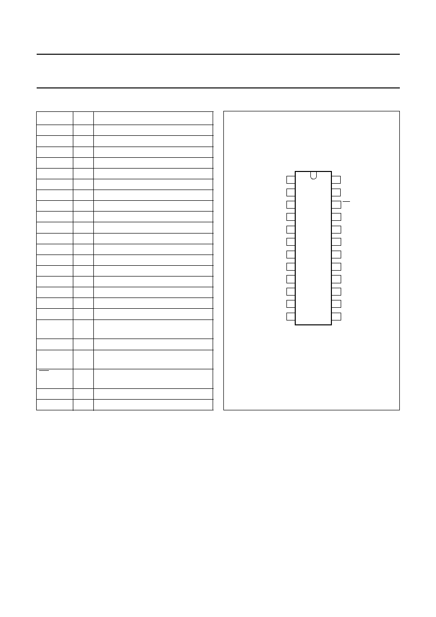
Fig.2 Pin configuration.
handbook, halfpage
1
2
3
4
5
6
7
8
9
10
11
12
24
23
22
21
20
19
18
17
16
15
14
13
TDA8714
D2
D3
D1
D0
n.c.
O/UF
D7
VCCO1
OGND
AGND
n.c.
VRB
CLK
D4
D5
D6
DGND
CE
VCCD
VCCA
V
VRT
n.c.
MSA667
CCO2
V I
1997 Oct 29
5
Philips Semiconductors
Product specification
8-bit high-speed analog-to-digital converter
TDA8714
LIMITING VALUES
In accordance with the Absolute Maximum Rating System (IEC 134).
Note
1. The supply voltages V
CCA
and V
CCD
may have any value between
-
0.3 V and +7.0 V provided the difference
between V
CCA
and V
CCD
is between
-
1 V and +1 V.
HANDLING
Inputs and outputs are protected against electrostatic discharges in normal handling. However, to be totally safe, it is
desirable to take normal precautions appropriate to handling integrated circuits.
THERMAL CHARACTERISTICS
SYMBOL
PARAMETER
CONDITIONS
MIN.
MAX.
UNIT
V
CCA
analog supply voltage
note 1
-
0.3
+7.0
V
V
CCD
digital supply voltage
note 1
-
0.3
+7.0
V
V
CCO
output stages supply voltage
note 1
-
0.3
+7.0
V
V
CC
supply voltage differences between
V
CCA
and V
CCD
-
1.0
+1.0
V
V
CC
supply voltage differences between
V
CCO
and V
CCD
-
1.0
+1.0
V
V
CC
supply voltage differences between
V
CCA
and V
CCO
-
1.0
+1.0
V
V
I
input voltage
referenced to AGND
-
0.3
+7.0
V
V
clk(p-p)
AC input voltage for switching
(peak-to-peak value)
referenced to DGND
-
V
CCD
V
I
O
output current
-
10
mA
T
stg
storage temperature
-
55
+150
∞
C
T
amb
operating ambient temperature
0
+70
∞
C
T
j
junction temperature
-
+150
∞
C
SYMBOL
PARAMETER
VALUE
UNIT
R
th j-a
thermal resistance from junction to ambient in free air
SOT137-1
75
K/W
SOT340-1
119
K/W
1997 Oct 29
6
Philips Semiconductors
Product specification
8-bit high-speed analog-to-digital converter
TDA8714
CHARACTERISTICS
V
CCA
= V
7
to V
6
= 4.75 to 5.25 V; V
CCD
= V
18
to V
17
= 4.75 to 5.25 V; V
CCO
= V
19
and V
21
to V
20
= 4.75 to 5.25 V;
AGND and DGND shorted together; V
CCA
to V
CCD
=
-
0.25 to +0.25 V; V
CCO
to V
CCD
=
-
0.25 to +0.25 V;
V
CCA
to V
CCO
=
-
0.25 to +0.25 V; V
i(p-p)
= 1.75 V; T
amb
= 0 to +70
∞
C; typical values measured at
V
CCA
= V
CCD
= V
CCO
= 5 V and T
amb
= 25
∞
C; unless otherwise specified.
SYMBOL
PARAMETER
CONDITIONS
MIN.
TYP.
MAX.
UNIT
Supply
V
CCA
analog supply voltage
4.75
5.0
5.25
V
V
CCD
digital supply voltage
4.75
5.0
5.25
V
V
CCO
output stages supply voltage
4.75
5.0
5.25
V
I
CCA
analog supply current
-
25
30
mA
I
CCD
digital supply current
-
27
33
mA
I
CCO
output stages supply current
-
16
20
mA
Inputs
C
LOCK INPUT
CLK (
REFERENCED TO
DGND); note 1
V
IL
LOW level input voltage
0
-
0.8
V
V
IH
HIGH level input voltage
2.0
-
V
CCD
V
I
IL
LOW level input current
V
clk
= 0.4 V
-
400
-
-
µ
A
I
IH
HIGH level input current
V
clk
= 2.7 V
-
-
300
µ
A
Z
I
input impedance
f
clk
= 80 MHz
-
18
-
k
C
I
input capacitance
f
clk
= 80 MHz
-
1
-
pF
I
NPUT
CE (
REFERENCED TO
DGND); see Table 2
V
IL
LOW level input voltage
0
-
0.8
V
V
IH
HIGH level input voltage
2.0
-
V
CCD
V
I
IL
LOW level input current
V
IL
= 0.4 V
-
400
-
-
µ
A
I
IH
HIGH level input current
V
IH
= 2.7 V
-
-
20
µ
A
V
I
(
ANALOG INPUT VOLTAGE REFERENCED TO
AGND)
I
IL
LOW level input current
V
I
= 1.2 V
-
0
-
µ
A
I
IH
HIGH level input current
V
I
= 3.5 V
60
130
280
µ
A
Z
I
input impedance
f
i
= 4.43 MHz
-
10
-
k
C
I
input capacitance
f
i
= 4.43 MHz
-
14
-
pF
Reference voltages for the resistor ladder; see Table 1
V
RB
reference voltage BOTTOM
1.2
1.3
1.6
V
V
RT
reference voltage TOP
3.5
3.6
3.9
V
V
diff
differential reference voltage V
RT
-
V
RB
1.9
2.3
2.7
V
I
ref
reference current
-
11.5
-
mA
R
LAD
resistor ladder
-
200
-
TC
RLAD
temperature coefficient of the resistor ladder
-
0.24
-
ppm
V
osB
offset voltage BOTTOM
note 2
275
285
295
mV
V
osT
offset voltage TOP
note 2
305
315
325
mV
V
i(p-p)
analog input voltage (peak-to-peak value)
1.45
1.75
2.15
V
1997 Oct 29
7
Philips Semiconductors
Product specification
8-bit high-speed analog-to-digital converter
TDA8714
Outputs
D
IGITAL OUTPUTS
D7 to D0 (
REFERENCED TO
DGND)
V
OL
LOW level output voltage
I
O
= 1 mA
0
-
0.4
V
V
OH
HIGH level output voltage
I
O
=
-
0.4 mA
2.7
-
V
CCD
V
I
O
=
-
1 mA
2.4
-
V
CCD
V
I
OZ
output current in 3-state mode
0.4 V < V
O
< V
CCD
-
20
-
+20
µ
A
Switching characteristics
C
LOCK INPUT
CLK (note 1; see Fig.3)
f
clk(max)
maximum clock frequency
TDA8714/4
40
-
-
MHz
TDA8714/6
60
-
-
MHz
TDA8714/7
80
-
-
MHz
t
CPH
clock pulse width HIGH
6
-
-
ns
t
CPL
clock pulse width LOW
6
-
-
ns
Analog signal processing
L
INEARITY
INL
DC integral non-linearity
-
±
0.4
±
0.5
LSB
DNL
DC differential non-linearity
-
±
0.2
±
0.35
LSB
AINL
AC integral non-linearity
note 3
-
±
0.5
±
1.0
LSB
B
ANDWIDTH
(f
clk
= 40 MHz); note 4
B
analog bandwidth
full-scale sine wave
-
13
-
MHz
75% full-scale sine
wave; small signal at
V
i
=
±
5 LSB, code 128
-
20
-
MHz
t
STLH
analog input settling time LOW-to-HIGH
full-scale square
wave; Fig.6; note 5
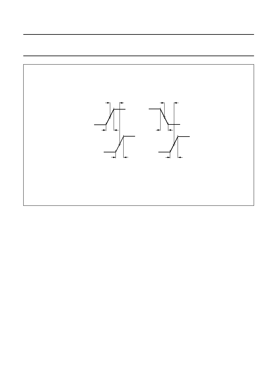
-
2.5
3.5
ns
t
STHL
analog input settling time HIGH-to-LOW
full-scale square
wave; Fig.6; note 5
-
3.0
4.0
ns
H
ARMONICS
(f
clk
= 40 MHz)
h
1
fundamental harmonics (full scale)
f
i
= 4.43 MHz
-
-
0
dB
h
all
harmonics (full scale);
all components
f
i
= 4.43 MHz
second harmonics
-
-
64
-
60
dB
third harmonics
-
-
58
-
55
dB
THD
total harmonic distortion
f
i
= 4.43 MHz
-
-
56
-
dB
S
IGNAL
-
TO
-
NOISE RATIO
(note 6; see Figs 7 and 13)
S/N
signal-to-noise ratio (full scale)
without harmonics;
f
clk
= 40 MHz;
f
i
= 4.43 MHz
46
48
-
dB
SYMBOL
PARAMETER
CONDITIONS
MIN.
TYP.
MAX.
UNIT
1997 Oct 29
8
Philips Semiconductors
Product specification
8-bit high-speed analog-to-digital converter
TDA8714
E
FFECTIVE BITS
(note 6; see Figs 7 and 13)
EB
effective bits
TDA8714/4
f
clk
= 40 MHz
f
i
= 4.43 MHz
-
7.75
-
bits
f
i
= 7.5 MHz
-
7.6
-
bits
effective bits
TDA8714/6
f
clk
= 60 MHz
f
i
= 4.43 MHz
-
7.7
-
bits
f
i
= 7.5 MHz
-
7.55
-
bits
f
i
= 10 MHz
-
7.4
-
bits
effective bits
TDA8714/7
f
clk
= 80 MHz
f
i
= 4.43 MHz
-
7.7
-
bits
f
i
= 7.5 MHz
-
7.5
-
bits
f
i
= 10 MHz
-
7.2
-
bits
f
i
= 15 MHz
-
6.3
-
bits
T
WO
-
TONE
(note 7)
TTIR
two-tone intermodulation rejection
f
clk
= 40 MHz
-
-
56
-
dB
B
IT ERROR RATE
BER
bit error rate
f
clk
= 40 MHz;
f
i
= 4.43 MHz;
V
I
=
±
16 LSB at
code 128
-
10
-
11
-
times/
samples
D
IFFERENTIAL GAIN
(note 8)
G
diff
differential gain
f
clk
= 40 MHz;
f
i
= 4.43 MHz
-
0.6
-
%
D
IFFERENTIAL PHASE
(note 8)
diff
differential phase
f
clk
= 40 MHz;
f
i
= 4.43 MHz
-
0.8
-
deg
Timing (note 9; see Figs 3 and 5; f
clk
= 80 MHz)
t
ds
sampling delay time
-
-
2
ns
t
h
output hold time
5
-
-
ns
t
d
output delay time
-
10
11
ns
3-state output delay times (see Fig.4)
t
dZH
enable HIGH
-
40
44
ns
t
dZL
enable LOW
-
12
16
ns
t
dHZ
disable HIGH
-
50
54
ns
t
dLZ
disable LOW
-
10
14
ns
SYMBOL
PARAMETER
CONDITIONS
MIN.
TYP.
MAX.
UNIT

1997 Oct 29
9
Philips Semiconductors
Product specification
8-bit high-speed analog-to-digital converter
TDA8714
Notes to the characteristics
1. In addition to a good layout of the digital and analog ground, it is recommended that the rise and fall times of the clock
must not be less than 1 ns.
2. Analog input voltages producing code 00 up to and including FF:
a) V
osB
(voltage offset BOTTOM) is the difference between the analog input which produces data equal to 00 and
the reference voltage BOTTOM (V
RB
) at T
amb
= 25
∞
C.
b) V
osT
(voltage offset TOP) is the difference between V
RT
(reference voltage TOP) and the analog input which
produces data outputs equal to FF at T
amb
= 25
∞
C.
3. Full-scale sine wave (f
i
= 4.43 MHz; f
clk
= 80 MHz).
4. The analog bandwidth is defined as the maximum input sine wave frequency which can be applied to the device.
No glitches greater than 2 LSBs, neither any significant attenuation are observed in the reconstructed signal.
5. The analog input settling time is the minimum time required for the input signal to be stabilized after a sharp full-scale
input (square-wave signal) in order to sample the signal and obtain correct output data.
6. Effective bits are obtained via a Fast Fourier Transform (FFT) treatment taking 8K acquisition points per equivalent
fundamental period. The calculation takes into account all harmonics and noise up to half of the clock frequency
(NYQUIST frequency). Conversion to signal-to-noise ratio: S/N = EB
◊
6.02 + 1.76 dB.
7. Intermodulation measured relative to either tone with analog input frequencies of 4.43 MHz and 4.53 MHz. The two
input signals have the same amplitude and the total amplitude of both signals provides full scale to the converter.
8. Measurement carried out using video analyser VM700A where the video analog signal is reconstructed through a
digital-to-analog converter.
9. Output data acquisition: the output data is available after the maximum delay time of t
d
; in the event of 80 MHz clock
operation, the hardware design must take into account the t
d
and t
h
limits with respect to the input characteristics of
the acquisition circuit.

1997 Oct 29
10
Philips Semiconductors
Product specification
8-bit high-speed analog-to-digital converter
TDA8714
Table 1
Output coding and input voltage (typical values; referenced to AGND)
Table 2
Mode selection
STEP
V
I(p-p)
O/UF
BINARY OUTPUT BITS
D7
D6
D5
D4
D3
D2
D1
D0
Underflow
<
1.585
1
0
0
0
0
0
0
0
0
0
1.585
0
0
0
0
0
0
0
0
0
1
.
0
0
0
0
0
0
0
0
1
.
.
.
.
.
.
.
.
.
.
.
.
.
.
.
.
.
.
.
.
.
254
.
0
1
1
1
1
1
1
1
0
255
3.28
0
1
1
1
1
1
1
1
1
Overflow
>
3.28
1
1
1
1
1
1
1
1
1
CE
D7 to D0
O/UF
1
high impedance
high impedance
0
active; binary
active
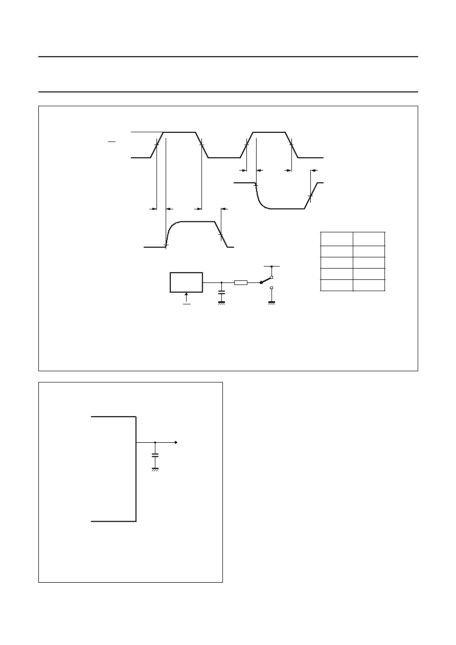
Fig.3 Timing diagram.
handbook, full pagewidth
ds
t
sample N + 1
sample N
CLK
MSA670
sample N + 2
50 %
V
l
DATA
D0 to D7
t d
t h
CPH
t
CPL
t
VDDO
0 V
50 %
DATA
N + 1
DATA
N
DATA
N - 1
DATA
N - 2
1997 Oct 29
11
Philips Semiconductors
Product specification
8-bit high-speed analog-to-digital converter
TDA8714
dbook, full pagewidth
MBD876
50 %
50 %
HIGH
LOW
dZH
t
dHZ
t
50 %
HIGH
LOW
dZL
t
dLZ
t
10 %
90 %
output
data
VCCD
output
data
3.3 k
15 pF
S1
VCCD
TDA8714
CE
CE
Fig.4 Timing diagram and test conditions of 3-state output delay time.
TEST
S1
t
dLZ
V
CCD
t
dZL
V
CCD
t
dHZ
DGND
t
dZH
DGND
f
CE
= 100 kHz.
Fig.5 Load circuit for timing measurement.
handbook, halfpage
MBB956 - 1
D0 to D7
15 pF
1997 Oct 29
12
Philips Semiconductors
Product specification
8-bit high-speed analog-to-digital converter
TDA8714
Fig.6 Analog input settling-time diagram.
handbook, full pagewidth
MGD184
50 %
STLH
t
2 ns
code 0
code 255
I
50 %
0.5 ns
50 %
2 ns
STHL
t
50 %
0.5 ns
CLK
V
1997 Oct 29
13
Philips Semiconductors
Product specification
8-bit high-speed analog-to-digital converter
TDA8714
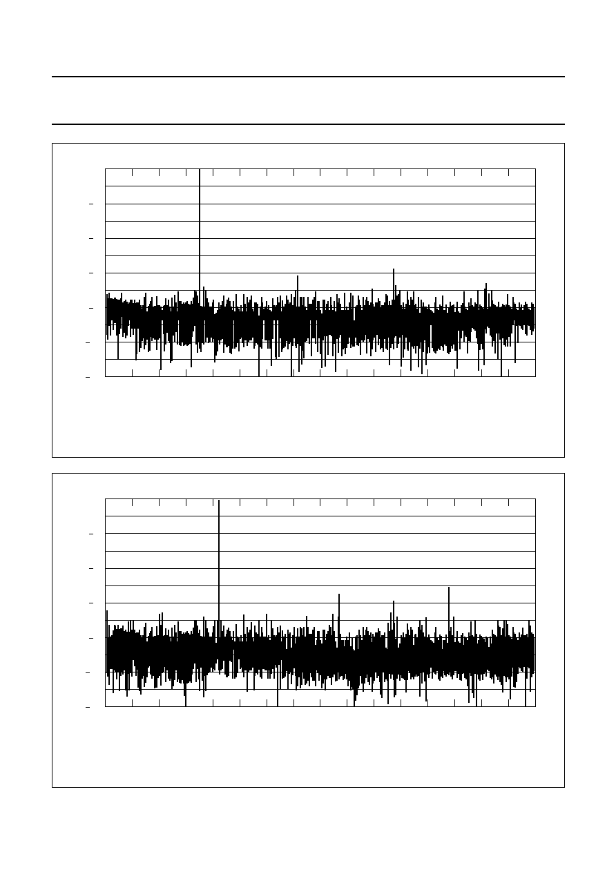
Fig.7 Fast Fourier Transform (f
clk
= 40 MHz; f
i
= 4.43 MHz).
Effective bits: 7.80; THD =
-
57.82 dB.
Harmonic levels (dB): 2nd =
-
68.00; 3rd =
-
61.54; 4th =
-
72.46; 5th =
-
65.80; 6th =
-
68.88.
handbook, full pagewidth
7.50
0
120
0
2.50
5.00
MBD877
40
80
17.5
10.0
12.5
15.0
20.0
f (MHz)
100
20
60
amplitude
(dB)
Fig.8 Fast Fourier Transform (f
clk
= 80 MHz; f
i
= 10 MHz).
Effective bits: 7.27; THD =
-
49.23 dB.
Harmonic levels (dB): 2nd =
-
56.16; 3rd =
-
51.01; 4th =
-
69.84; 5th =
-
59.10; 6th =
-
65.34.
handbook, full pagewidth
14.1
0
120
0
4.69
9.39
MBD878
40
80
32.9
18.8
23.5
28.2
37.5
f (MHz)
100
20
60
amplitude
(dB)

1997 Oct 29
14
Philips Semiconductors
Product specification
8-bit high-speed analog-to-digital converter
TDA8714
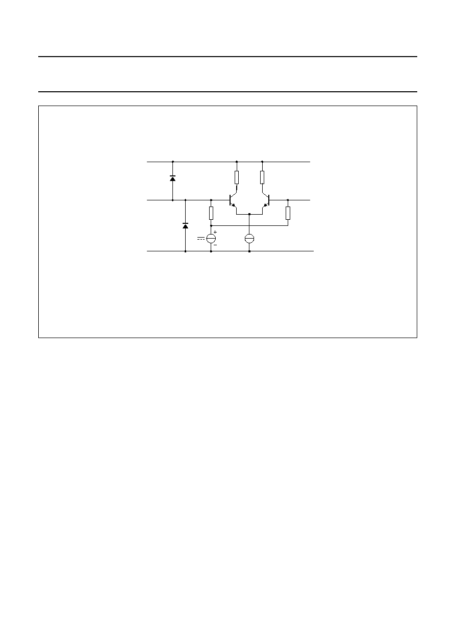
INTERNAL PIN CONFIGURATIONS
Fig.9 TTL data and overflow/underflow outputs.
handbook, halfpage
MLB036
DGND
D7 to D0
O/UF
VCCO2
VCCO1
Fig.10 Analog inputs.
handbook, halfpage
MLB037
AGND
V CCA
(x 90)
V I
Fig.11 CE (3-state) input.
book, halfpage
MLB038
DGND
VCCO1
CE
Fig.12 V
RB
and V
RT
.
handbook, halfpage
R
MEA050 - 1
AGND
VRB
VRM
VCCA
VRT
LAD
1997 Oct 29
15
Philips Semiconductors
Product specification
8-bit high-speed analog-to-digital converter
TDA8714
Fig.13 CLK input.
handbook, full pagewidth
30 k
30 k
V
VCCD
CLK
DGND
MCD189 - 1
ref
1997 Oct 29
16
Philips Semiconductors
Product specification
8-bit high-speed analog-to-digital converter
TDA8714
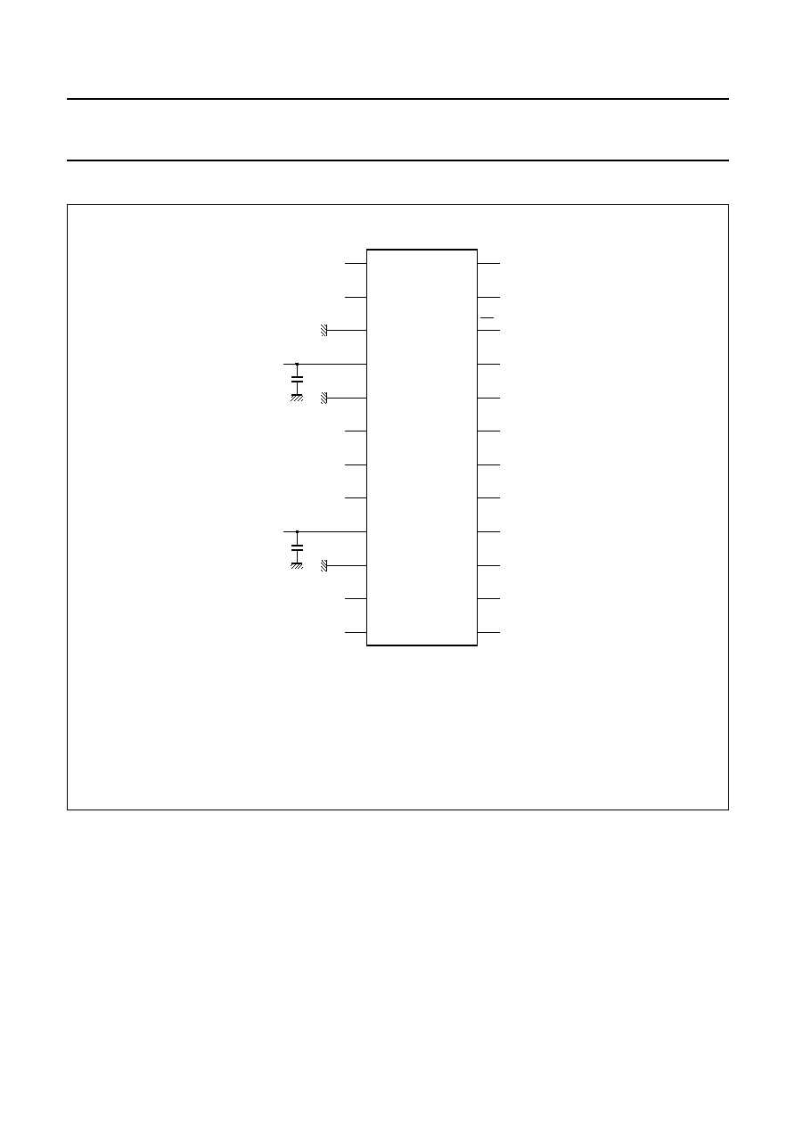
APPLICATION INFORMATION
Fig.14 Application diagram.
The analog and digital supplies should be separated and decoupled.
The external voltage generator must be built such that a good supply voltage ripple rejection is achieved with respect to the LSB value.
(1) V
RB
and V
RT
are decoupled to AGND.
(2) Pin 5 should be connected to AGND; pins 3 and 10 to DGND in order to prevent noise influence.
handbook, halfpage
24
23
22
21
20
19
18
17
16
15
14
13
TDA8714
D2
D3
VCCO1
OGND
CLK
D4
D5
D6
VCCD
1
2
3
4
5
6
7
8
9
10
11
12
D1
D0
n.c.
O/UF
D7
AGND
n.c.
VRB
VCCA
VRT
n.c.
MSA668
100 nF
100 nF
DGND
CE
VCCO2
AGND
AGND
V I
(2)
(1)
(2)
(1)
(2)
1997 Oct 29
17
Philips Semiconductors
Product specification
8-bit high-speed analog-to-digital converter
TDA8714
PACKAGE OUTLINES
UNIT
A
max.
A
1
A
2
A
3
b
p
c
D
(1)
E
(1)
(1)
e
H
E
L
L
p
Q
Z
y
w
v
REFERENCES
OUTLINE
VERSION
EUROPEAN
PROJECTION
ISSUE DATE
IEC
JEDEC
EIAJ
mm
inches
2.65
0.30
0.10
2.45
2.25
0.49
0.36
0.32
0.23
15.6
15.2
7.6
7.4
1.27
10.65
10.00
1.1
1.0
0.9
0.4
8
0
o
o
0.25
0.1
DIMENSIONS (inch dimensions are derived from the original mm dimensions)
Note
1. Plastic or metal protrusions of 0.15 mm maximum per side are not included.
1.1
0.4
SOT137-1
X
12
24
w
M
A
A
1
A
2
b
p
D
H
E
L
p
Q
detail X
E
Z
c
L
v
M
A
13
(A )
3
A
y
0.25
075E05
MS-013AD
pin 1 index
0.10
0.012
0.004
0.096
0.089
0.019
0.014
0.013
0.009
0.61
0.60
0.30
0.29
0.050
1.4
0.055
0.419
0.394
0.043
0.039
0.035
0.016
0.01
0.25
0.01
0.004
0.043
0.016
0.01
e
1
0
5
10 mm
scale
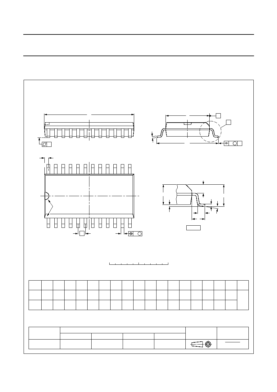
SO24: plastic small outline package; 24 leads; body width 7.5 mm
SOT137-1
95-01-24
97-05-22
1997 Oct 29
18
Philips Semiconductors
Product specification
8-bit high-speed analog-to-digital converter
TDA8714
UNIT
A
1
A
2
A
3
b
p
c
D
(1)
E
(1)
(1)
e
H
E
L
L
p
Q
Z
y
w
v
REFERENCES
OUTLINE
VERSION
EUROPEAN
PROJECTION
ISSUE DATE
IEC
JEDEC
EIAJ
mm
0.21
0.05
1.80
1.65
0.38
0.25
0.20
0.09
8.4
8.0
5.4
5.2
0.65
1.25
7.9
7.6
0.9
0.7
0.8
0.4
8
0
o
o
0.13
0.1
0.2
DIMENSIONS (mm are the original dimensions)
Note
1. Plastic or metal protrusions of 0.20 mm maximum per side are not included.
1.03
0.63
SOT340-1
MO-150AG
93-09-08
95-02-04
X
w
M
A
A
1
A
2
b
p
D
H
E
L
p
Q
detail X
E
Z
e
c
L
v
M
A
(A )
3
A
1
12
24
13
0.25
y
pin 1 index
0
2.5
5 mm
scale
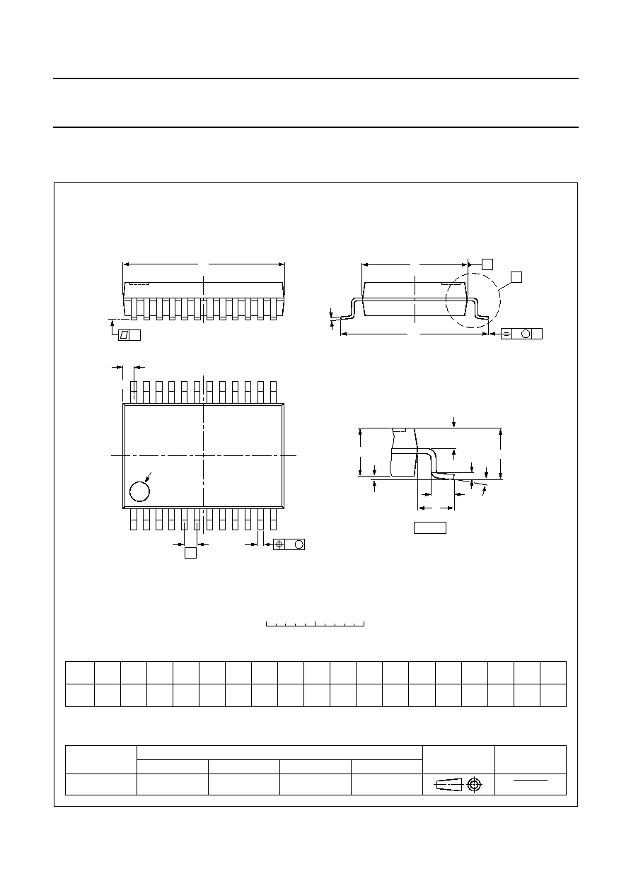
SSOP24: plastic shrink small outline package; 24 leads; body width 5.3 mm
SOT340-1
A
max.
2.0

1997 Oct 29
19
Philips Semiconductors
Product specification
8-bit high-speed analog-to-digital converter
TDA8714
SOLDERING
Introduction
There is no soldering method that is ideal for all IC
packages. Wave soldering is often preferred when
through-hole and surface mounted components are mixed
on one printed-circuit board. However, wave soldering is
not always suitable for surface mounted ICs, or for
printed-circuits with high population densities. In these
situations reflow soldering is often used.
This text gives a very brief insight to a complex technology.
A more in-depth account of soldering ICs can be found in
our
"IC Package Databook" (order code 9398 652 90011).
Reflow soldering
Reflow soldering techniques are suitable for all SO and
SSOP packages.
Reflow soldering requires solder paste (a suspension of
fine solder particles, flux and binding agent) to be applied
to the printed-circuit board by screen printing, stencilling or
pressure-syringe dispensing before package placement.
Several techniques exist for reflowing; for example,
thermal conduction by heated belt. Dwell times vary
between 50 and 300 seconds depending on heating
method. Typical reflow temperatures range from
215 to 250
∞
C.
Preheating is necessary to dry the paste and evaporate
the binding agent. Preheating duration: 45 minutes at
45
∞
C.
Wave soldering
SO
Wave soldering techniques can be used for all SO
packages if the following conditions are observed:
∑
A double-wave (a turbulent wave with high upward
pressure followed by a smooth laminar wave) soldering
technique should be used.
∑
The longitudinal axis of the package footprint must be
parallel to the solder flow.
∑
The package footprint must incorporate solder thieves at
the downstream end.
SSOP
Wave soldering is not recommended for SSOP packages.
This is because of the likelihood of solder bridging due to
closely-spaced leads and the possibility of incomplete
solder penetration in multi-lead devices.
If wave soldering cannot be avoided, the following
conditions must be observed:
∑
A double-wave (a turbulent wave with high upward
pressure followed by a smooth laminar wave)
soldering technique should be used.
∑
The longitudinal axis of the package footprint must
be parallel to the solder flow and must incorporate
solder thieves at the downstream end.
Even with these conditions, only consider wave
soldering SSOP packages that have a body width of
4.4 mm, that is SSOP16 (SOT369-1) or
SSOP20 (SOT266-1).
M
ETHOD
(SO
AND
SSOP)
During placement and before soldering, the package must
be fixed with a droplet of adhesive. The adhesive can be
applied by screen printing, pin transfer or syringe
dispensing. The package can be soldered after the
adhesive is cured.
Maximum permissible solder temperature is 260
∞
C, and
maximum duration of package immersion in solder is
10 seconds, if cooled to less than 150
∞
C within
6 seconds. Typical dwell time is 4 seconds at 250
∞
C.
A mildly-activated flux will eliminate the need for removal
of corrosive residues in most applications.
Repairing soldered joints
Fix the component by first soldering two diagonally-
opposite end leads. Use only a low voltage soldering iron
(less than 24 V) applied to the flat part of the lead. Contact
time must be limited to 10 seconds at up to 300
∞
C. When
using a dedicated tool, all other leads can be soldered in
one operation within 2 to 5 seconds between
270 and 320
∞
C.

1997 Oct 29
20
Philips Semiconductors
Product specification
8-bit high-speed analog-to-digital converter
TDA8714
DEFINITIONS
LIFE SUPPORT APPLICATIONS
These products are not designed for use in life support appliances, devices, or systems where malfunction of these
products can reasonably be expected to result in personal injury. Philips customers using or selling these products for
use in such applications do so at their own risk and agree to fully indemnify Philips for any damages resulting from such
improper use or sale.
Data sheet status
Objective specification
This data sheet contains target or goal specifications for product development.
Preliminary specification
This data sheet contains preliminary data; supplementary data may be published later.
Product specification
This data sheet contains final product specifications.
Limiting values
Limiting values given are in accordance with the Absolute Maximum Rating System (IEC 134). Stress above one or
more of the limiting values may cause permanent damage to the device. These are stress ratings only and operation
of the device at these or at any other conditions above those given in the Characteristics sections of the specification
is not implied. Exposure to limiting values for extended periods may affect device reliability.
Application information
Where application information is given, it is advisory and does not form part of the specification.

1997 Oct 29
21
Philips Semiconductors
Product specification
8-bit high-speed analog-to-digital converter
TDA8714
NOTES

1997 Oct 29
22
Philips Semiconductors
Product specification
8-bit high-speed analog-to-digital converter
TDA8714
NOTES

1997 Oct 29
23
Philips Semiconductors
Product specification
8-bit high-speed analog-to-digital converter
TDA8714
NOTES

Internet: http://www.semiconductors.philips.com
Philips Semiconductors ≠ a worldwide company
© Philips Electronics N.V. 1997
SCA55
All rights are reserved. Reproduction in whole or in part is prohibited without the prior written consent of the copyright owner.
The information presented in this document does not form part of any quotation or contract, is believed to be accurate and reliable and may be changed
without notice. No liability will be accepted by the publisher for any consequence of its use. Publication thereof does not convey nor imply any license
under patent- or other industrial or intellectual property rights.
Netherlands: Postbus 90050, 5600 PB EINDHOVEN, Bldg. VB,
Tel. +31 40 27 82785, Fax. +31 40 27 88399
New Zealand: 2 Wagener Place, C.P.O. Box 1041, AUCKLAND,
Tel. +64 9 849 4160, Fax. +64 9 849 7811
Norway: Box 1, Manglerud 0612, OSLO,
Tel. +47 22 74 8000, Fax. +47 22 74 8341
Philippines: Philips Semiconductors Philippines Inc.,
106 Valero St. Salcedo Village, P.O. Box 2108 MCC, MAKATI,
Metro MANILA, Tel. +63 2 816 6380, Fax. +63 2 817 3474
Poland: Ul. Lukiska 10, PL 04-123 WARSZAWA,
Tel. +48 22 612 2831, Fax. +48 22 612 2327
Portugal: see Spain
Romania: see Italy
Russia: Philips Russia, Ul. Usatcheva 35A, 119048 MOSCOW,
Tel. +7 095 755 6918, Fax. +7 095 755 6919
Singapore: Lorong 1, Toa Payoh, SINGAPORE 1231,
Tel. +65 350 2538, Fax. +65 251 6500
Slovakia: see Austria
Slovenia: see Italy
South Africa: S.A. PHILIPS Pty Ltd., 195-215 Main Road Martindale,
2092 JOHANNESBURG, P.O. Box 7430 Johannesburg 2000,
Tel. +27 11 470 5911, Fax. +27 11 470 5494
South America: Rua do Rocio 220, 5th floor, Suite 51,
04552-903 S„o Paulo, S√O PAULO - SP, Brazil,
Tel. +55 11 821 2333, Fax. +55 11 829 1849
Spain: Balmes 22, 08007 BARCELONA,
Tel. +34 3 301 6312, Fax. +34 3 301 4107
Sweden: Kottbygatan 7, Akalla, S-16485 STOCKHOLM,
Tel. +46 8 632 2000, Fax. +46 8 632 2745
Switzerland: Allmendstrasse 140, CH-8027 ZÐRICH,
Tel. +41 1 488 2686, Fax. +41 1 481 7730
Taiwan: Philips Semiconductors, 6F, No. 96, Chien Kuo N. Rd., Sec. 1,
TAIPEI, Taiwan Tel. +886 2 2134 2865, Fax. +886 2 2134 2874
Thailand: PHILIPS ELECTRONICS (THAILAND) Ltd.,
209/2 Sanpavuth-Bangna Road Prakanong, BANGKOK 10260,
Tel. +66 2 745 4090, Fax. +66 2 398 0793
Turkey: Talatpasa Cad. No. 5, 80640 GÐLTEPE/ISTANBUL,
Tel. +90 212 279 2770, Fax. +90 212 282 6707
Ukraine: PHILIPS UKRAINE, 4 Patrice Lumumba str., Building B, Floor 7,
252042 KIEV, Tel. +380 44 264 2776, Fax. +380 44 268 0461
United Kingdom: Philips Semiconductors Ltd., 276 Bath Road, Hayes,
MIDDLESEX UB3 5BX, Tel. +44 181 730 5000, Fax. +44 181 754 8421
United States: 811 East Arques Avenue, SUNNYVALE, CA 94088-3409,
Tel. +1 800 234 7381
Uruguay: see South America
Vietnam: see Singapore
Yugoslavia: PHILIPS, Trg N. Pasica 5/v, 11000 BEOGRAD,
Tel. +381 11 625 344, Fax.+381 11 635 777
For all other countries apply to: Philips Semiconductors, Marketing & Sales Communications,
Building BE-p, P.O. Box 218, 5600 MD EINDHOVEN, The Netherlands, Fax. +31 40 27 24825
Argentina: see South America
Australia: 34 Waterloo Road, NORTH RYDE, NSW 2113,
Tel. +61 2 9805 4455, Fax. +61 2 9805 4466
Austria: Computerstr. 6, A-1101 WIEN, P.O. Box 213, Tel. +43 160 1010,
Fax. +43 160 101 1210
Belarus: Hotel Minsk Business Center, Bld. 3, r. 1211, Volodarski Str. 6,
220050 MINSK, Tel. +375 172 200 733, Fax. +375 172 200 773
Belgium: see The Netherlands
Brazil: see South America
Bulgaria: Philips Bulgaria Ltd., Energoproject, 15th floor,
51 James Bourchier Blvd., 1407 SOFIA,
Tel. +359 2 689 211, Fax. +359 2 689 102
Canada: PHILIPS SEMICONDUCTORS/COMPONENTS,
Tel. +1 800 234 7381
China/Hong Kong: 501 Hong Kong Industrial Technology Centre,
72 Tat Chee Avenue, Kowloon Tong, HONG KONG,
Tel. +852 2319 7888, Fax. +852 2319 7700
Colombia: see South America
Czech Republic: see Austria
Denmark: Prags Boulevard 80, PB 1919, DK-2300 COPENHAGEN S,
Tel. +45 32 88 2636, Fax. +45 31 57 0044
Finland: Sinikalliontie 3, FIN-02630 ESPOO,
Tel. +358 9 615800, Fax. +358 9 61580920
France: 4 Rue du Port-aux-Vins, BP317, 92156 SURESNES Cedex,
Tel. +33 1 40 99 6161, Fax. +33 1 40 99 6427
Germany: Hammerbrookstraþe 69, D-20097 HAMBURG,
Tel. +49 40 23 53 60, Fax. +49 40 23 536 300
Greece: No. 15, 25th March Street, GR 17778 TAVROS/ATHENS,
Tel. +30 1 4894 339/239, Fax. +30 1 4814 240
Hungary: see Austria
India: Philips INDIA Ltd, Band Box Building, 2nd floor,
254-D, Dr. Annie Besant Road, Worli, MUMBAI 400 025,
Tel. +91 22 493 8541, Fax. +91 22 493 0966
Indonesia: see Singapore
Ireland: Newstead, Clonskeagh, DUBLIN 14,
Tel. +353 1 7640 000, Fax. +353 1 7640 200
Israel: RAPAC Electronics, 7 Kehilat Saloniki St, PO Box 18053,
TEL AVIV 61180, Tel. +972 3 645 0444, Fax. +972 3 649 1007
Italy: PHILIPS SEMICONDUCTORS, Piazza IV Novembre 3,
20124 MILANO, Tel. +39 2 6752 2531, Fax. +39 2 6752 2557
Japan: Philips Bldg 13-37, Kohnan 2-chome, Minato-ku, TOKYO 108,
Tel. +81 3 3740 5130, Fax. +81 3 3740 5077
Korea: Philips House, 260-199 Itaewon-dong, Yongsan-ku, SEOUL,
Tel. +82 2 709 1412, Fax. +82 2 709 1415
Malaysia: No. 76 Jalan Universiti, 46200 PETALING JAYA, SELANGOR,
Tel. +60 3 750 5214, Fax. +60 3 757 4880
Mexico: 5900 Gateway East, Suite 200, EL PASO, TEXAS 79905,
Tel. +9-5 800 234 7381
Middle East: see Italy
Printed in The Netherlands
547047/1200/06/pp24
Date of release: 1997 Oct 29
Document order number:
9397 750 02956