Document Outline
- 1 FEATURES
- 2 APPLICATIONS
- 3 GENERAL DESCRIPTION
- 4 QUICK REFERENCE DATA
- 5 ORDERING INFORMATION
- 6 BLOCK DIAGRAM
- 7 PINNING
- 8 LIMITING VALUES
- 9 THERMAL CHARACTERISTICS
- 10 CHARACTERISTICS
- 11 APPLICATION INFORMATION
- 11.1 Output coding and control signals
- 11.2 TDA8769 in 3G radio receivers
- 11.3 Application diagrams
- 11.4 Demonstration board
- 11.5 Definitions
- 11.5.1 NON-LINEAR PARAMETERS
- 11.5.1.1 Integral non-linearity, INL
- 11.5.1.2 Differential non-linearity, DNL
- 11.5.2 DYNAMIC PARAMETERS, SINGLE TONE
- 11.5.2.1 Signal-to-noise and distortion, SINAD
- 11.5.2.2 Effective number of bits, ENOB
- 11.5.2.3 Total harmonic distortion, THD
- 11.5.2.4 Signal-to-noise ratio, SNR
- 11.5.2.5 Spurious free dynamic range, SFDR
- 11.5.3 INTERMODULATION PARAMETERS, DUAL TONE
- 11.5.3.1 Spectral analysis (dual tone)
- 11.5.3.2 Intermodulation distortion, IMD2 and IMD3
- 11.5.4 NOISE POWER RATIO
- 12 PACKAGE OUTLINE
- 13 SOLDERING
- 13.1 Introduction to soldering surface mount packages
- 13.2 Reflow soldering
- 13.3 Wave soldering
- 13.4 Manual soldering
- 13.5 Suitability of surface mount IC packages for wave and reflow soldering methods
- 14 DATA SHEET STATUS
- 15 DEFINITIONS
- 16 DISCLAIMERS

DATA SHEET
Objective specification
2003 Apr 07
INTEGRATED CIRCUITS
TDA8769
12-bit, 80/105 Msps
Analog-to-Digital Converter (ADC)
Nyquist/High IF sampling

2003 Apr 07
2
Philips Semiconductors
Objective specification
12-bit, 80/105 Msps Analog-to-Digital
Converter (ADC) Nyquist/High IF sampling
TDA8769
CONTENTS
1
FEATURES
2
APPLICATIONS
3
GENERAL DESCRIPTION
4
QUICK REFERENCE DATA
5
ORDERING INFORMATION
6
BLOCK DIAGRAM
7
PINNING
8
LIMITING VALUES
9
THERMAL CHARACTERISTICS
10
CHARACTERISTICS
11
APPLICATION INFORMATION
11.1
Output coding and control signals
11.2
TDA8769 in 3G radio receivers
11.3
Application diagrams
11.4
Demonstration board
11.5
Definitions
11.5.1
Non-linear parameters
11.5.1.1
Integral non-linearity, INL
11.5.1.2
Differential non-linearity, DNL
11.5.2
Dynamic parameters, single tone
11.5.2.1
Signal-to-noise and distortion, SINAD
11.5.2.2
Effective number of bits, ENOB
11.5.2.3
Total harmonic distortion, THD
11.5.2.4
Signal-to-noise ratio, SNR
11.5.2.5
Spurious free dynamic range, SFDR
11.5.3
Intermodulation parameters, dual tone
11.5.3.1
Spectral analysis (dual tone)
11.5.3.2
Intermodulation distortion, IMD2 and IMD3
11.5.4
Noise power ratio
12
PACKAGE OUTLINE
13
SOLDERING
13.1
Introduction to soldering surface mount
packages
13.2
Reflow soldering
13.3
Wave soldering
13.4
Manual soldering
13.5
Suitability of surface mount IC packages for
wave and reflow soldering methods
14
DATA SHEET STATUS
15
DEFINITIONS
16
DISCLAIMERS

2003 Apr 07
3
Philips Semiconductors
Objective specification
12-bit, 80/105 Msps Analog-to-Digital
Converter (ADC) Nyquist/High IF sampling
TDA8769
1
FEATURES
∑
12-bit resolution
∑
Optimized for both Nyquist and High IF sampling
∑
High-speed sampling rate up to 105 MHz
∑
Maximum analog input frequency of 250 MHz
∑
Only 2 clock cycles latency
∑
5 V power supplies and 3.3 V output power supply
∑
Binary or two's-complement CMOS outputs
∑
Programmable Complete Conversion Signal (CCS)
CMOS output
∑
In-range CMOS-compatible output
∑
TLL and CMOS-compatible static digital inputs
∑
TTL and CMOS-compatible digital outputs
∑
Differential clock input PECL; sine wave and TTL
compatible
∑
Integrated track-and-hold amplifier
∑
Differential analog input
∑
External amplitude range control
∑
Full-scale controllable from 1.5 to 1.9 V (p-p)
∑
Voltage controlled regulator included
∑
Temperature range from
-
40 to +85
∞
C.
2
APPLICATIONS
∑
Cellular infrastructure (2.5G, 3G, etc.)
∑
Base stations and "Zero-IF" or direct IF sampling
subsystems
∑
Wireless and wired broadband communications
∑
Wireless Local Loop (WLL)
∑
Local Multipoint Distribution Service (LMDS)
∑
Advanced Frequency Modulation (FM) radio
∑
Imaging (camera scanner and medical)
∑
Cable modem or set top box
∑
Radar and satellite hub systems.
3
GENERAL DESCRIPTION
The TDA8769 is a BiCMOS 12-bit Analog-to-Digital
Converter (ADC) optimized for GSM/EDGE, W-CDMA and
CDMA2000 radio transceivers, high data rate radios and
other applications such as advanced FM radio and
professional imaging. Its main innovation is the RF
sampling, based on a high-speed clock of up to 105 Msps
combined with high input frequencies of up to 250 MHz.
It converts the analog input signal into 12-bit binary coded
digital words at a maximum sampling rate of 105 MHz.
The TDA8769 analog performances have been proven in
various multi-carrier 3G radio receivers, providing the
best-in-class Adjacent Channel Selectivity (ACS) up to
80 dB.
Moreover the TDA8769 offers the lowest clock cycle
latency, which enables competitive and optimized
feedback loops in controlled systems.
All static digital inputs (TH, CEN, OTC, DEL0 and DEL1)
are CMOS compatible and all outputs are TTL-CMOS
compatible. A sine wave clock input signal can also be
used.
4
QUICK REFERENCE DATA
Tbf.
5
ORDERING INFORMATION
TYPE NUMBER
PACKAGE
SAMPLING
FREQUENCY
(MHz)
NAME
DESCRIPTION
VERSION
TDA8769HW/8
HTQFP48
plastic thermal enhanced thin quad flat package;
48 leads; body 7
◊
7
◊
1.0 mm; heatsink
SOT545-2
80
TDA8769HW/10
105
2003 Apr 07
4
Philips Semiconductors
Objective specification
12-bit, 80/105 Msps Analog-to-Digital
Converter (ADC) Nyquist/High IF sampling
TDA8769
6
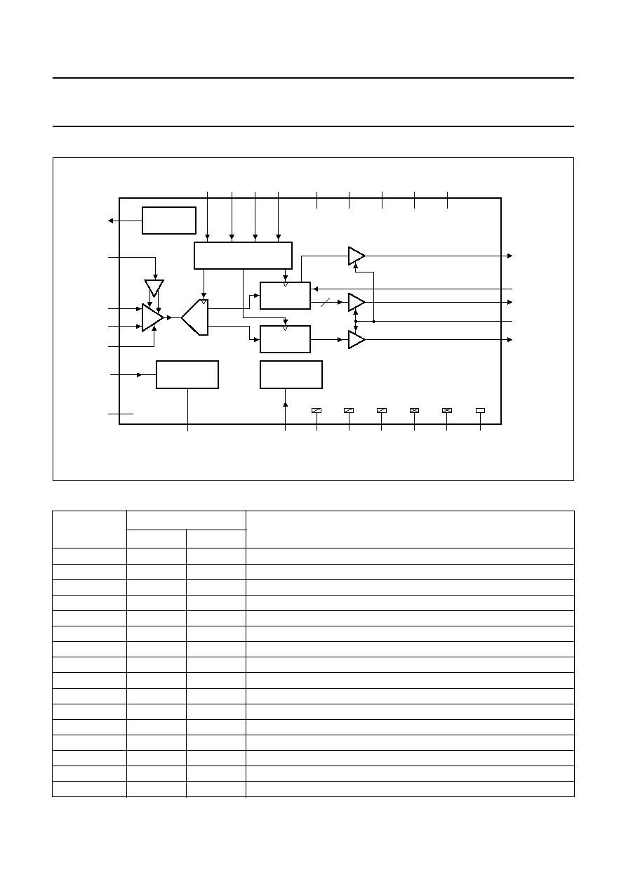
BLOCK DIAGRAM
handbook, full pagewidth
MBL884
12
VREF
REFERENCE
CLOCK
DRIVER
POWER
MANAGEMENT
CMADC
REFERENCE
LATCH
LATCH
ADC
&
AMP
FSREF
D0 to D11
VCCO
CEN
DEC
13
11
47
46
42
1
16
38
35
20
5
19
23 to 34
22
IR
OTC
DEL0
CLKN
2
VCCA1
3
VCCA3
44
VCCA4
40
VCCD1
17
VCCD2
VREF
INN
IN
TH
CMADC
TDA8769
TRACK
HOLD
n.c.
6 to 10, 12,
14, 21, 45
AGND1
48
AGND3
4
AGND4
43
DGND1
41
DGND2
18
OGND
37
CCS
39
CLK
15
DEL1
36
Fig.1 Block diagram.
7
PINNING
SYMBOL
PIN
DESCRIPTION
NUMBER
TYPE
(1)
CMADC
1
I
regulator output common mode ADC input
V
CCA1
2
P
analog supply voltage 1 (5.0 V)
V
CCA3
3
P
analog supply voltage 3 (5.0 V)
AGND3
4
G
analog ground 3
DEC
5
I/O
decoupling node
n.c.
6
-
not connected
n.c.
7
-
not connected
n.c.
8
-
not connected
n.c.
9
-
not connected
n.c.
10
-
not connected
VREF
11
I
reference voltage input
n.c.
12
-
not connected
FSREF
13
O
reference output
n.c.
14
-
not connected
DEL1
15
I
complete conversion sampling delay input 1
DEL0
16
I
complete conversion sampling delay input 0

2003 Apr 07
5
Philips Semiconductors
Objective specification
12-bit, 80/105 Msps Analog-to-Digital
Converter (ADC) Nyquist/High IF sampling
TDA8769
Note
1. P = power supply;
G = ground;
I = input;
O = output.
V
CCD2
17
P
digital supply voltage 2 (5.0 V)
DGND2
18
G
digital ground 2
OTC
19
I
control input two's complement output (active HIGH)
CEN
20
I
chip enable input (CMOS level; active LOW)
n.c.
21
-
not connected
IR
22
O
in-range output
D11
23
O
data output bit 11 (MSB)
D10
24
O
data output bit 10
D9
25
O
data output bit 9
D8
26
O
data output bit 8
D7
27
O
data output bit 7
D6
28
O
data output bit 6
D5
29
O
data output bit 5
D4
30
O
data output bit 4
D3
31
O
data output bit 3
D2
32
O
data output bit 2
D1
33
O
data output bit 1
D0
34
O
data output bit 0 (LSB)
V
CCO
35
P
supply voltage of data output (3.3 V)
CCS
36
O
complete conversion signal output
OGND
37
G
ground of data output
CLKN
38
I
complementary clock input
CLK
39
I
clock input
V
CCD1
40
P
digital supply voltage 1 (5.0 V)
DGND1
41
G
digital ground 1
TH
42
I
track-and-hold enable input (CMOS level; active HIGH)
AGND4
43
G
analog ground 4
V
CCA4
44
P
analog supply voltage 4 (5.0 V)
n.c.
45
-
not connected
IN
46
I
analog input voltage
INN
47
I
complementary analog input voltage
AGND1
48
G
analog ground 1
AGND5
heatsink
G
analog ground 5
SYMBOL
PIN
DESCRIPTION
NUMBER
TYPE
(1)

2003 Apr 07
6
Philips Semiconductors
Objective specification
12-bit, 80/105 Msps Analog-to-Digital
Converter (ADC) Nyquist/High IF sampling
TDA8769
handbook, full pagewidth
TDA8769HW
MBL885
1
2
3
4
5
6
7
8
9
10
11
12
36
35
34
33
32
31
30
29
28
27
26
25
13
14
15
16
17
18
19
20
21
22
23
24
48
47
46
45
44
43
42
41
40
39
38
37
AGND1
INN
IN
n.c.
V
CCA4
AGND4
TH
DGND1
V
CCD1
CLK
CLKN
OGND
FSREF
n.c.
DEL1
DEL0
V
CCD2
DGND2
OTC
CEN
n.c.
IR
D11
D10
CMADC
VCCA1
VCCA3
AGND3
DEC
n.c.
n.c.
n.c.
n.c.
n.c.
VREF
n.c.
CCS
VCCO
D0
D1
D2
D3
D4
D5
D6
D7
D8
D9
Fig.1 Pin configuration.
8
LIMITING VALUES
Tbf.
9
THERMAL CHARACTERISTICS
SYMBOL
PARAMETER
CONDITIONS
VALUE
UNIT
R
th(j-a)
thermal resistance from junction
to ambient
in free air; (tbf)
25
K/W
R
th(c-a)
thermal resistance from case to
ambient
in free air; (tbf)
(tbf)
K/W

2003
Apr
07
7
Philips Semiconductors
Objectiv
e specification
12-bit, 80/105
Msps Analog-to-Digital
Con
v
e
r
ter (ADC) Nyquist/High IF sampling
TD
A8769
This text is here in white to force landscape pages to be rotated correctly when browsing through the pdf in the Acrobat reader.This text is here in
_
white to force landscape pages to be rotated correctly when browsing through the pdf in the Acrobat reader.This text is here inThis text is here in
white to force landscape pages to be rotated correctly when browsing through the pdf in the Acrobat reader. white to force landscape pages to be ...
10 CHARACTERISTICS
V
CCA
= 4.75 to 5.25 V; V
CCD
= 4.75 to 5.25 V; V
CCO
= 3.0 to 3.6 V; AGND connected to DGND; T
amb
=
-
40 to +85
∞
C; V
IN(p
-
p)
-
V
INN(p
-
p)
= 1.9 V;
V
VREF
= V
CCA3
-
1.75 V; V
i(CM )
= V
CCA3
-
1.6 V; typical values measured at V
CCA
= V
CCD
= 5 V and V
CCO
= 3.3 V; T
amb
= 25
∞
C and C
L
= 10 pF;
unless otherwise specified.
SYMBOL
PARAMETER
CONDITIONS
TEST
(1)
MIN.
TYP.
MAX.
UNIT
Supplies
V
CCA
analog supply voltage
-
4.75
5.0
5.25
V
V
CCD
digital supply voltage
-
4.75
5.0
5.25
V
V
CCO
output supply voltage
-
3.0
3.3
3.6
V
I
CCA
analog supply current
-
-
109
(tbf)
mA
I
CCD
digital supply current
-
-
48
(tbf)
mA
I
CCO
output supply current
f
CLK
= 80 Msps; f
i
= 20 MHz
-
-
17.5
(tbf)
mA
P
tot
total power dissipation
f
CLK
= 80 Msps; f
i
= 20 MHz
-
-
840
(tbf)
mW
f
CLK
= 105 Msps; f
i
= 20 MHz
-
-
(tbf)
(tbf)
mW
Clock inputs: pins CLK and CLKN; note 2
I
NPUTS
V
IL
LOW-level input voltage referenced to DGND; V
CCD
= 5 V
-
PECL mode
-
3.19
-
3.52
V
TTL mode
-
DGND
-
0.8
V
V
IH
HIGH-level input
voltage
referenced to DGND; V
CCD
= 5 V
-
PECL mode
-
3.83
-
4.12
V
TTL mode
-
2.0
-
V
CCD
V
I
IL
LOW-level input current V
CLK
or V
CLKN
= 3.19 V
-
(tbf)
-
-
µ
A
V
CLK
or V
CLKN
= 2.00 V
-
(tbf)
-
-
mA
I
IH
HIGH-level input
current
V
CLK
or V
CLKN
= 3.83 V
-
-
-
(tbf)
µ
A
V
CLK
or V
CLKN
= 0.80 V
-
-
-
(tbf)
mA
V
CLK
differential AC input
voltage for switching
(V
CLK
-
V
CLKN
)
AC mode; DC voltage level = 2.5 V
-
(tbf)
1.5
(tbf)
V
R
i
input resistance
f
CLK
= 105 Msps
-
(tbf)
-
-
k
C
i
input capacitance
f
CLK
= 105 Msps
-
-
-
(tbf)
pF

2003
Apr
07
8
Philips Semiconductors
Objectiv
e specification
12-bit, 80/105
Msps Analog-to-Digital
Con
v
e
r
ter (ADC) Nyquist/High IF sampling
TD
A8769
This text is here in white to force landscape pages to be rotated correctly when browsing through the pdf in the Acrobat reader.This text is here in
_
white to force landscape pages to be rotated correctly when browsing through the pdf in the Acrobat reader.This text is here inThis text is here in
white to force landscape pages to be rotated correctly when browsing through the pdf in the Acrobat reader. white to force landscape pages to be ...
T
IMING
f
clk(min)
minimum clock
frequency
V
TH
= V
CCD
-
-
-
(tbf)
Msps
f
clk(max)
maximum clock
frequency
-
105
-
-
Msps
t
CLKH
clock HIGH pulse width
f
clk
= 25 MHz
-
(tbf)
-
-
ns
t
CLKL
clock LOW pulse width
f
clk
= 25 MHz
-
(tbf)
-
-
ns
Analog inputs: pins IN and INN
I
IL
LOW-level input current V
VREF
= V
CCA3
-
1.75 V;
V
TH
= HIGH
-
-
(tbf)
-
µ
A
I
IH
HIGH-level input
current
V
VREF
= V
CCA3
-
1.75 V;
V
TH
= HIGH
-
-
(tbf)
-
µ
A
R
i
input resistance
f
i
= 25 MHz
D
-
8.4
-
M
C
i
input capacitance
f
i
= 25 MHz
D
-
250
-
fF
V
i(CM)
common mode input
voltage
V
IN
= V
INN
; output code = 2047
-
(tbf)
V
CCA3
-
1.6
(tbf)
V
Digital inputs: pins OTC, SH, DEL1, DEL0 and CEN
V
IL
LOW-level input voltage
-
DGND
-
0.8
V
V
IH
HIGH-level input
voltage
-
2.0
-
V
CCD
V
I
IL
LOW-level input current V
IL
= 0.8 V
-
(tbf)
-
µ
A
I
IH
HIGH-level input
current
V
IH
= 2.0 V
-
-
-
(tbf)
µ
A
Voltage controlled regulator input: pin CMADC
V
o(CM)
common mode output
voltage
-
-
V
CCA3
-
1.6
-
V
I
load
load current
-
-
(tbf)
(tbf)
mA
Reference voltage input: pin VREF; note 3
V
i
full-scale fixed voltage
f
i
= 25 MHz; f
CLK
= 105 Msps
-
-
V
CCA3
-
1.75
-
V
I
i
input current
-
-
(tbf)
(tbf)
µ
A
V
i(IN-INN)(p-p)
input voltage
(peak-to-peak value)
V
VREF
= V
CCA3
-
1.75 V;
V
(IN-INN)(CM)
= V
CCA3
-
1.6 V
-
-
1.9
-
V
SYMBOL
PARAMETER
CONDITIONS
TEST
(1)
MIN.
TYP.
MAX.
UNIT
2003
Apr
07
9
Philips Semiconductors
Objectiv
e specification
12-bit, 80/105
Msps Analog-to-Digital
Con
v
e
r
ter (ADC) Nyquist/High IF sampling
TD
A8769
This text is here in white to force landscape pages to be rotated correctly when browsing through the pdf in the Acrobat reader.This text is here in
_
white to force landscape pages to be rotated correctly when browsing through the pdf in the Acrobat reader.This text is here inThis text is here in
white to force landscape pages to be rotated correctly when browsing through the pdf in the Acrobat reader. white to force landscape pages to be ...
Full-scale voltage controlled regulator output: pin FSREF
V
o(FS)
1.9 V full-scale output
voltage
-
-
V
CCA3
-
1.75
-
V
Digital outputs: pins D11 to D0 and IR
O
UTPUT LEVELS
V
OL
LOW-level output
voltage
I
OL
= 2 mA
-
DGND
-
DGND + 0.5
V
V
OH
HIGH-level output
voltage
I
OH
=
-
0.4 mA
-
V
CCO
-
0.5
-
V
CCO
V
I
OZ
output current in 3-state output level between 0.5 V and
V
CCO
-
(tbf)
-
(tbf)
µ
A
T
IMING
; see Fig. 2
t
d(s)
sampling delay
C
L
= 10 pF; note 4
-
-
(tbf)
(tbf)
ns
t
h(o)
output hold time
C
L
= 10 pF
-
(tbf)
(tbf)
-
ns
t
d(o)
output delay
C
L
= 10 pF
-
-
(tbf)
(tbf)
ns
3-
STATE OUTPUT DELAY
t
dZH
enable to HIGH state
-
-
(tbf)
(tbf)
ns
t
dZL
enable to LOW state
-
-
(tbf)
(tbf)
ns
t
dHZ
disable from HIGH
state
-
-
(tbf)
(tbf)
ns
t
dLZ
disable from LOW state
-
-
(tbf)
(tbf)
ns
Timing complete conversion signal: pin CCS
t
d(CCS)
complete conversion
signal delay
C
L
= 10 pF; see Table 4 and Fig. 3
-
DEL0 = LOW; DEL1 = HIGH
-
-
0
-
ns
DEL0 = HIGH; DEL1 = LOW
-
-
1.2
-
ns
DEL0 = HIGH; DEL1 = HIGH
-
-
2.2
-
ns
Analog signal processing (50% clock duty factor)
INL
integral non-linearity
f
CLK
= 20 Msps; f
i
= 400 kHz
-
-
±
1.4
(tbf)
LSB
DNL
differential non-linearity
f
CLK
= 20 Msps; f
i
= 400 kHz; no
missing code guaranteed
-
-
±
0.4
(tbf)
LSB
E
offset
offset error
V
CCA
= V
CCD
= 5 V; V
CCO
= 3.3 V;
T
amb
= 25
∞
C; output code = 2047
-
(tbf)
(tbf)
(tbf)
mV
SYMBOL
PARAMETER
CONDITIONS
TEST
(1)
MIN.
TYP.
MAX.
UNIT

2003
Apr
07
10
Philips Semiconductors
Objectiv
e specification
12-bit, 80/105
Msps Analog-to-Digital
Con
v
e
r
ter (ADC) Nyquist/High IF sampling
TD
A8769
This text is here in white to force landscape pages to be rotated correctly when browsing through the pdf in the Acrobat reader.This text is here in
_
white to force landscape pages to be rotated correctly when browsing through the pdf in the Acrobat reader.This text is here inThis text is here in
white to force landscape pages to be rotated correctly when browsing through the pdf in the Acrobat reader. white to force landscape pages to be ...
E
G
gain error amplitude;
spread from device to
device
V
CCA
= V
CCD
= 5 V; V
CCO
= 3.3 V;
T
amb
= 25
∞
C
-
(tbf)
-
(tbf)
%FS
B
analog bandwidth
f
CLK
= 105 Msps;
-
3 dB; full-scale
input; note 5
-
(tbf)
250
-
MHz
THD
total harmonic
distortion
TDA8769HW/8; note 6
-
f
i
= 21.4 MHz; B = Nyquist
-
-
-
70.4
-
dBFS
f
i
= 50 MHz; B = Nyquist
-
-
-
70.0
-
dBFS
TDA8769HW/10; note 6
-
f
i
= 21.4 MHz; B = Nyquist
-
-
-
69.2
-
dBFS
f
i
= 78 MHz; B = Nyquist
-
-
-
63
-
dBFS
N
th(rms)
thermal noise (RMS
value)
shorted input; V
TH
= V
CCD
;
f
clk
= 105 Msps
-
-
(tbf)
-
LSB
SNR
signal-to-noise ratio
TDA8769HW/8; note 7
-
f
i
= 21.4 MHz; B = Nyquist
-
-
65.8
-
dBc
f
i
= 50 MHz; B = Nyquist
-
-
65.2
-
dBc
f
i
= 50 MHz; B = 5 MHz
-
-
72.4
-
dBc
TDA8769HW/10; note 7
-
f
i
= 21.4 MHz; B = Nyquist
-
-
64.1
-
dBc
f
i
= 78 MHz; B = Nyquist
-
-
62.1
-
dBc
f
i
= 78 MHz; B = 5 MHz
-
-
71.7
-
dBc
SFDR
spurious free dynamic
range
TDA8769HW/8
-
f
i
= 21.4 MHz; B = Nyquist
-
-
71.6
-
dBc
f
i
= 50 MHz; B = Nyquist
-
-
72.1
-
dBc
f
i
= 50 MHz; B = 5 MHz
-
-
80.8
-
dBc
TDA8769HW/10
-
f
i
= 21.4 MHz; B = Nyquist
-
-
72
-
dBc
f
i
= 78 MHz; B = Nyquist
-
-
64.8
-
dBc
f
i
= 78 MHz; B = 5 MHz
-
-
82.6
-
dBc
SYMBOL
PARAMETER
CONDITIONS
TEST
(1)
MIN.
TYP.
MAX.
UNIT

2003
Apr
07
11
Philips Semiconductors
Objectiv
e specification
12-bit, 80/105
Msps Analog-to-Digital
Con
v
e
r
ter (ADC) Nyquist/High IF sampling
TD
A8769
This text is here in white to force landscape pages to be rotated correctly when browsing through the pdf in the Acrobat reader.This text is here in
_
white to force landscape pages to be rotated correctly when browsing through the pdf in the Acrobat reader.This text is here inThis text is here in
white to force landscape pages to be rotated correctly when browsing through the pdf in the Acrobat reader. white to force landscape pages to be ...
Notes
1. D = guaranteed by design.
2. The circuit has two clock inputs: CLK and CLKN. There are 5 modes of operation:
a) PECL mode 1: (DC level varies proportionally with V
CCD
) CLK and CLKN inputs are at differential PECL levels.
b) PECL mode 2: (DC level varies proportionally with V
CCD
) CLK input is at PECL level and sampling is taken on the falling edge of the clock input
signal. A DC level of 3.65 V has to be applied on CLKN decoupled to GND via a 100 nF capacitor.
c) PECL mode 3: (DC level varies proportionally with V
CCD
) CLKN input is at PECL level and sampling is taken on the rising edge of the clock input
signal. A DC level of 3.65 V has to be applied on CLK decoupled to GND via a 100 nF capacitor.
d) Differential AC driving mode 4: When driving the CLK input directly and with any AC signal of minimum 1 V (p-p) and with a DC level of 2.5 V,
the sampling takes place at the falling edge of the clock signal. When driving the CLKN input with the same signal, sampling takes place at the
rising edge of the clock signal. It is recommended to decouple the CLKN or CLK input to DGND via a 100 nF capacitor.
e) TTL mode 5: CLK input is at TTL level and sampling is taken on the falling edge of the clock input signal. In that case CLKN pin has to be
connected to the ground.
3. The ADC input range can be adjusted with an external reference connected to pin VREF. This voltage has to be referenced to V
CCA
.
4. Output data acquisition: the output data is available after the maximum delay of t
d(s)
.
ENOB
effective number of bits
TDA8769HW/8; note 8
-
f
i
= 21.4 MHz; B = Nyquist
-
-
10.4
-
bit
f
i
= 50 MHz; B = Nyquist
-
-
10.3
-
bit
f
i
= 50 MHz; B = 5 MHz
-
-
11.7
-
bit
TDA8769HW/10; note 8
-
f
i
= 21.4 MHz; B = Nyquist
-
-
10.2
-
bit
f
i
= 78 MHz; B = Nyquist
-
-
9.6
-
bit
f
i
= 78 MHz; B = 5 MHz
-
-
11.62
-
bit
TTIR
two-tone
intermodulation
rejection
f
clk
= 80 Msps; note 9
-
-
(tbf)
-
dBFS
f
clk
= 105 Msps; note 9
-
-
(tbf)
-
dBFS
f
i
= 15 or 18 MHz; f
clk
= 76.8 Msps;
note 9
-
-
68.73
-
dBFS
d
3
third order
intermodulation
distortion
f
i
= 21 or 24 MHz; note 10
-
dBFS
f
clk
= 76.8 Msps; (tbf)
-
-
68.87
-
dBFS
f
clk
= 80 Msps; (tbf)
-
-
(tbf)
-
dBFS
f
clk
= 105 Msps; (tbf)
-
-
(tbf)
-
dBFS
BER
bit error rate
f
i
= 25 MHz; V
IN
= 16LSB at code
2047; f
clk
= 105 Msps
-
-
(tbf)
-
SYMBOL
PARAMETER
CONDITIONS
TEST
(1)
MIN.
TYP.
MAX.
UNIT
2003 Apr 07
12
Philips Semiconductors
Objective specification
12-bit, 80/105 Msps Analog-to-Digital
Converter (ADC) Nyquist/High IF sampling
TDA8769
5. The
-
3 dB analog bandwidth is determined by the 3 dB reduction in the reconstructed output, the input being a
full-scale sine wave.
6. The total harmonic distortion is obtained with the addition of the first five harmonics.
7. The signal-to-noise ratio takes into account all harmonics above five and noise up to Nyquist frequency.
8. The effective number of bits, or ENOB, are obtained via a Fast Fourier Transform (FFT). The calculation takes into
account all harmonics and noise up to half of the clock frequency (Nyquist frequency). Conversion to signal-to-noise
and distortion, or SINAD, is given by SINAD = ENOB
◊
6.02 + 1.76 dB.
9. Intermodulation measured relative to either tone with analog input frequencies of (tbf) and (tbf) MHz. The two input
signals have the same amplitude and the total amplitude of both signals provides full-scale input to the converter
(-6 dB below full-scale for each input signal).
10. d
3
is the ratio of the RMS value of either input tone to the RMS value of the worst case third order intermodulation
product.
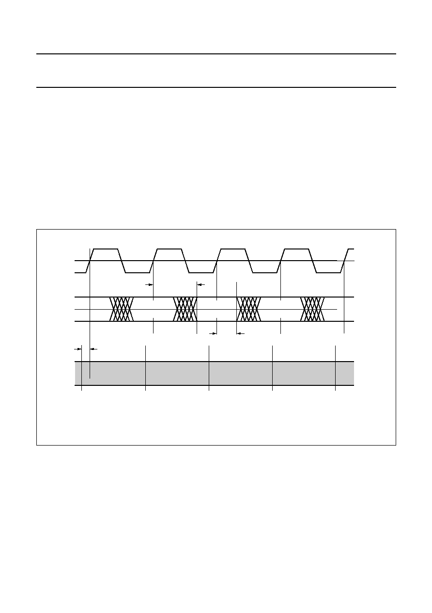
handbook, full pagewidth
VIN
CLK
0.5 V
n
D0 to D11
VCCO
-
0.5 V
50%
data
n
-
1
data
n
data
n
+
1
td(o)
td(s)
th(o)
MDB034
sample
n
sample
n
+
1
sample
n
+
2
sample
n
+
3
sample
n
+
4
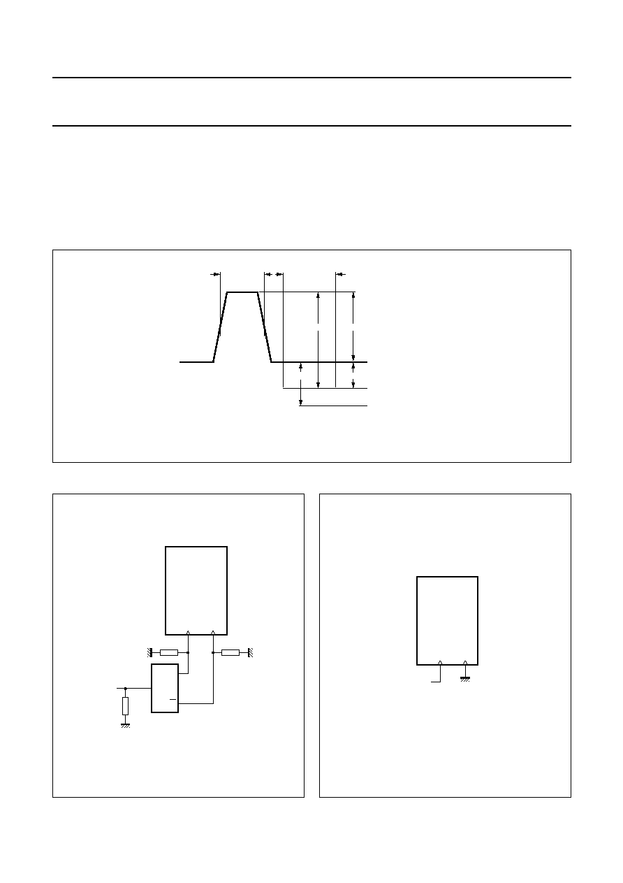
Fig.2 Output timing diagram.
2003 Apr 07
13
Philips Semiconductors
Objective specification
12-bit, 80/105 Msps Analog-to-Digital
Converter (ADC) Nyquist/High IF sampling
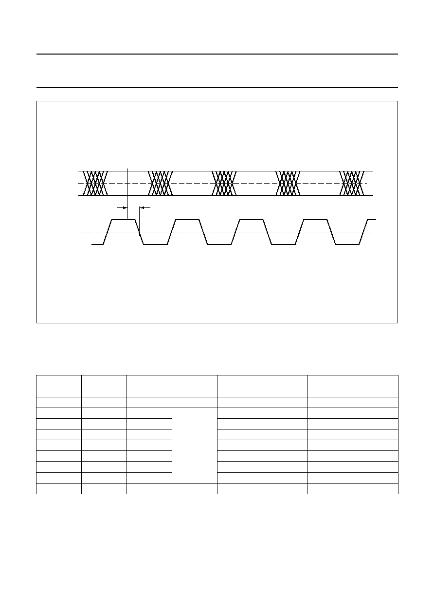
TDA8769
handbook, full pagewidth
MBL874
D0 to D11
CCS
td(CCS)
Fig.3 Complete conversion signal timing diagram.
11 APPLICATION INFORMATION
11.1
Output coding and control signals
Table 1
Output coding with differential inputs (typical values to AGND); V
IN(p
-
p)
-
V
INN(p
-
p)
= 1.9 V;
V
VREF
= V
CCA3
-
1.75 V
CODE
V
IN(p-p)
V
INN(p-p)
IR
BINARY OUTPUTS
(D11 TO D0)
TWO'S COMPLEMENT
OUTPUTS (D11 TO D0)
Underflow
<3.125
>4.075
0
0 0 0 0 0 0 0 0 0 0 0 0
1 0 0 0 0 0 0 0 0 0 0 0
0
3.125
4.075
1
0 0 0 0 0 0 0 0 0 0 0 0
1 0 0 0 0 0 0 0 0 0 0 0
1
-
-
0 0 0 0 0 0 0 0 0 0 0 1
1 0 0 0 0 0 0 0 0 0 0 1
:
:
:
:
:
2047
3.6
3.6
0 1 1 1 1 1 1 1 1 1 1 1
1 1 1 1 1 1 1 1 1 1 1 1
:
:
:
:
:
4094
-
-
1 1 1 1 1 1 1 1 1 1 1 0
0 1 1 1 1 1 1 1 1 1 1 0
4095
4.075
3.125
1 1 1 1 1 1 1 1 1 1 1 1
0 1 1 1 1 1 1 1 1 1 1 1
Overflow
>4.075
<3.125
0
1 1 1 1 1 1 1 1 1 1 1 1
0 1 1 1 1 1 1 1 1 1 1 1

2003 Apr 07
14
Philips Semiconductors
Objective specification
12-bit, 80/105 Msps Analog-to-Digital
Converter (ADC) Nyquist/High IF sampling
TDA8769
Table 2
Mode selection
Table 3
Track-and-hold selection
Table 4
Complete conversion signal selection
11.2
TDA8769 in 3G radio receivers
TDA8769 has been proven in many 3G receivers with various operating conditions regarding input frequency, signal
input frequency bandwidth and sampling frequency. TDA8769 provides a maximum analog input frequency of 250 MHz.
It allows a significant cost reduction of the RF front-end, from two mixers to only one, even in multicarrier architecture.
Table 5 shows possible applications with the TDA8769 in High IF sampling mode.
Table 5
Examples of possible f
i
, f
clk
and f
i
bandwidth combinations supported
CONTROL INPUT TWO'S
COMPLEMENT OUTPUT
(OTC)
CHIP ENABLE NOT (CEN)
OUTPUT DATA (D0 TO D11 AND IR)
0
0
binary; active
1
0
two's complement; active
don't care
1
high impedance
CONTROL INPUT TRACK-AND-HOLD (TH)
MODE
1
active
0
inactive; tracking
DEL1
DEL0
OUTPUT SIGNAL
0
0
inactive
0
1
active
1
0
1
1
f
i
(MHz)
f
clk
(MHz)
f
i
BW (MHz)
SNR (dB)
SFDR (dBc)
250
9.60
0.20
66.5
79.9
243.95
9.60
0.20
62.6
68.5
243.95
19.20
0.20
68.4
77.2
243.95
52.00
0.20
65.7
80.0
190
40.00
1.25
72.0
80.0
106
76.80
5.00
70.8
83.6
86
76.80
5.00
72.2
87.1
80
61.44
10.00
(tbf)
(tbf)
70
40.00
5.00
70
70
69.99
58.98
1.25
(tbf)
(tbf)
27
51.2
3.5
(tbf)
(tbf)
10.8
32.5
0.30
84.3
83.0
2003 Apr 07
15
Philips Semiconductors
Objective specification
12-bit, 80/105 Msps Analog-to-Digital
Converter (ADC) Nyquist/High IF sampling
TDA8769
For a dual carrier W_CDMA receiver, the most important parameters are the sensitivity and Adjacent Channel Selectivity
(ACS). In W-CDMA, it can be far below the noise floor, is defined by the Sensitivity to Noise Ratio (SENR). Its value is
negative due to the gain processing. The Adjacent Channel Power Ratio (ACPR) is the difference between the peak and
noise floor. It represents the ratio of the adjacent channel power and the average power of the channel. The ACS is
defined by the sum of SENR and ACPR. Figure 4 illustrates the relation between these parameters.
On a typical application with the TDA8769 device, the ACS obtained is 80 dB with an ACPR of 70 dB and a SENR of
10 dB. Moreover, the Noise Figure (NF) of the TDA8769 is 31.5 dB.
handbook, full pagewidth
MBL875
ACPR
NF
interfering
channel
wanted
channel
ACS
noise floor
sensitivity
thermal noise
SENR
Fig.4 Adjacent channel selectivity and analog-to-digital converter sensitivity.
11.3
Application diagrams
MDB035
Q
Q
D
TTL
270
270
50
TDA8769
CLKN
CLK
Fig.5 TTL to PECL translator application.
MDB036
TDA8769
CLKN
CLK
TTL
Fig.6 TTL single-ended clock application.
2003 Apr 07
16
Philips Semiconductors
Objective specification
12-bit, 80/105 Msps Analog-to-Digital
Converter (ADC) Nyquist/High IF sampling
TDA8769
11.4
Demonstration board
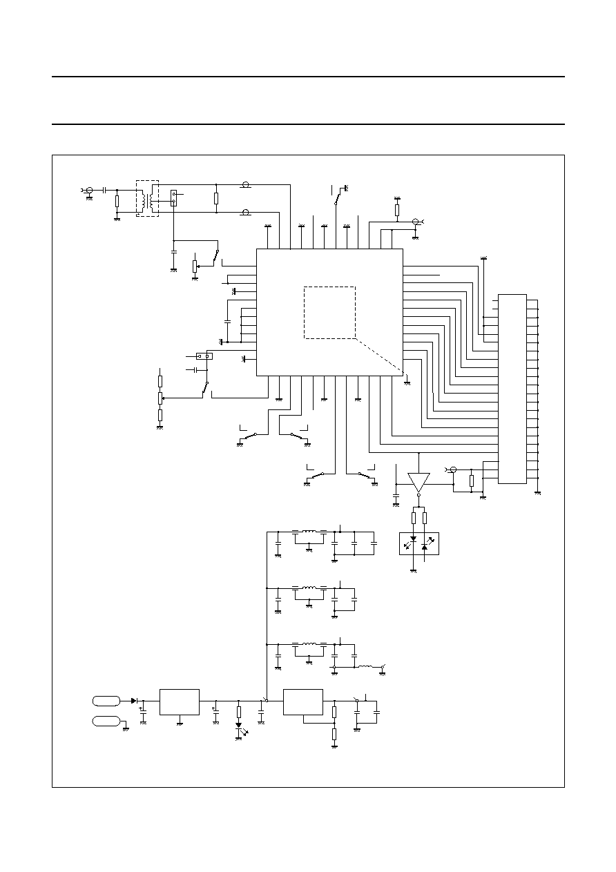
handbook, full pagewidth
MBL876
2
1
3
A1
A2
A3
A4
A5
A6
A7
A8
A9
A10
A11
A12
A13
A14
A15
A16
A17
A19
A18
A20
A21
A22
B1
B2
B3
B4
B5
B6
B7
B8
B9
B10
B11
B12
B13
B14
B15
B16
B17
B19
B18
B20
B21
B22
J1
36
TDA8769HW
35
CCS
VCCO
34
D0
33
D1
32
D2
31
D3
30
D4
29
D5
28
D6
27
D7
26
D8
25
D9
37
OGND
38
CLKN
39
CLK
40
V
CCD1
41
DGND1
42
TH
43
AGND4
44
V
CCA4
45
n.c.
46
IN
47
INN
48
AGND1
4
AGND3
5
DEC
6
n.c.
7
n.c.
8
n.c.
9
n.c.
10
n.c.
11
VREF
12
n.c.
24
23
22
21
20
19
18
17
16
15
14
13
D10
D11
IR
n.c.
CEN
OTC
DGND2
V
CCD2
DEL0
DEL1
n.c.
FSREF
IC1
VCCA (44)
C2
330
nF
C3
100
nF
FL1
470D_0D0_S
C18
10
nF
(2/3)
C19
10
nF
VCCD1 (40)
C13
330
nF
C15
100
nF
FL3
470D_0D0_S
C17
10
nF
VCCD2 (17)
C11
330
nF
C6
100
nF
FL2
470D_0D0_S
FL4
HF70A08S
C20
10
nF
TM2
TM3
OUT
OUT
ADJ
IN
3
2
1
VCCO (35)
C10
1
µ
F
C16
10
nF
LM317D2T
GND
IN
1
3
2
MC7805D2T
R8
R7
330
240
R6
750
TM1
C9
470
nF
D2
PWR
LGT679_C0
C8
4.7
µ
F
16 V
C7
22
µ
F
20 V
D1
BYD17G
J5
1
12 V
J5
2
GND
MSTBA2.5_20_5D8
IC3
IC2
D0
CSS
PCN12A_44P_2.54DS
S4
VCCD2
ON
DEL1
S8
VCCD2
ON
DEL0
VCCD2
S6
1K2
VCCD2
ON
OTC
S7
1K2
VCCD2
OFF
CEN
R125680
J3
TRIG
R9
50
VCCO
C12
10
nF
VCC
GND
2
3
5
4
IC4
R10
150
VCCO
IR
D3
LS6T670
R11
150
1
4
2
3
74AHC1GUO4GW
R125680
J2
R2
50
VCCD1
ON
1K2
TH
S1
VCCA
S3
EXT
1K2
VCCA
R4
2.4 k
P2
1 k
R5
1.2 k
C5
100 nF
C1
220 nF
VCCA
VCCA
1
2
CMADC
VCCA1
3
VCCA3
C4
100
nF
VCCA
TB2
S2
EXT
1K2
VCCA
P1
5 k
CMADC
C14
330
nF
TB1
VCCA
R3
100
R1
100
TR1
T1_6T_KK81
IN
R125680
J1
CLK
4
6
5
50
AGND
AGND
AGND
AGND
AGND
DGND
VCCD1
DGND
DGND
DGND
AGND
AGND
AGND
DGND
VCCO
AGND
DGND
AGND
AGND
AGND
DGND
DGND
DGND
DGND
DGND
DGND
DGND
DGND
DGND
DGND
TP1
DGND
DGND
DGND
DGND
AGND
DGND
DGND
DGND
DGND
DGND
DGND
DGND
DGND
DGND
DGND
AGND
AGND
AGND
Fig.7 Demonstration board schematic.
2003 Apr 07
17
Philips Semiconductors
Objective specification
12-bit, 80/105 Msps Analog-to-Digital
Converter (ADC) Nyquist/High IF sampling
TDA8769
handbook, full pagewidth
MBL877
R2
TM2
C1
J1
S1
S2
P1
1TB1
R1
TR1
IC1
R3
C3
C2
FL1
IC2
J5
21
D1
C7
TM3
J3
TM1
R5
D2
R6
C8
IC3
C10
TP1
C11
C12
R11
R10
P2
R7
R8
C9
C5
R4
D3
FL2
S3
S4
S5
S6
S7
R9
TB2
J4
J2
C4
C5
1
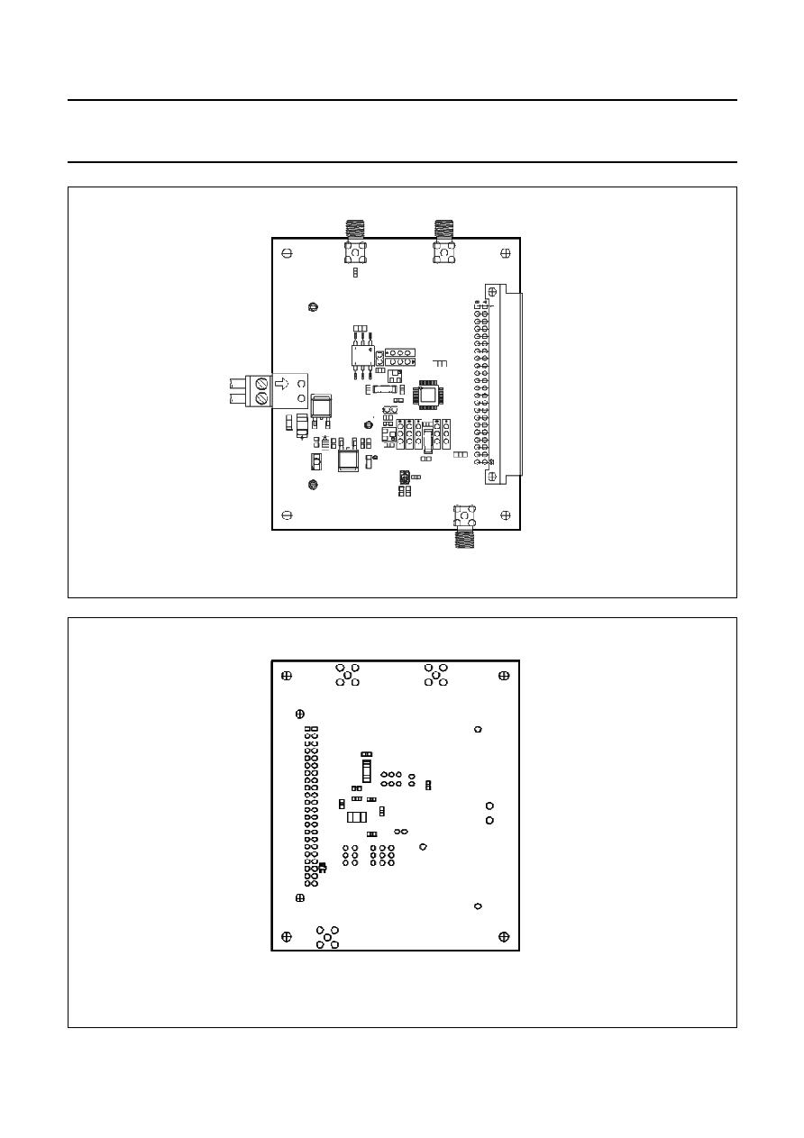
Fig.8 Component placement, top view.
handbook, full pagewidth
MBL878
IC4
C20
FL3
C13
C15
FL4
C18
C14
C19
C17
C16
Fig.9 Component placement, bottom view.
2003 Apr 07
18
Philips Semiconductors
Objective specification
12-bit, 80/105 Msps Analog-to-Digital
Converter (ADC) Nyquist/High IF sampling
TDA8769
handbook, full pagewidth
MBL879
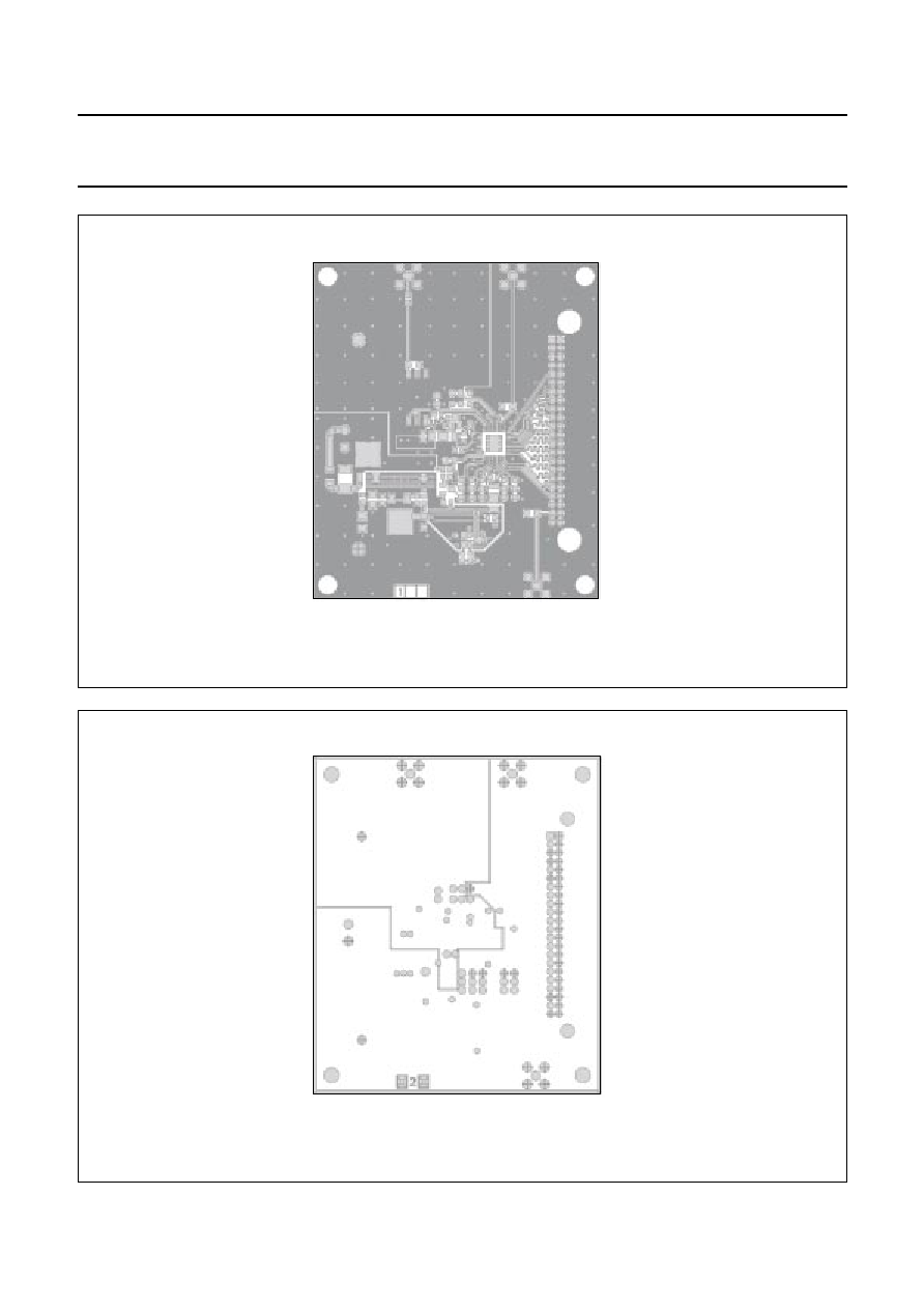
Fig.10 Printed-circuit board tracks, layout 1.
handbook, full pagewidth
MBL880
Fig.11 Printed-circuit board tracks, layout 2.

2003 Apr 07
19
Philips Semiconductors
Objective specification
12-bit, 80/105 Msps Analog-to-Digital
Converter (ADC) Nyquist/High IF sampling
TDA8769
handbook, full pagewidth
MBL881
Fig.12 Printed-circuit board tracks, layout 3.
11.5
Definitions
11.5.1
N
ON
-
LINEAR PARAMETERS
11.5.1.1
Integral non-linearity, INL
INL is defined as the deviation of the transfer function from
a best fit straight line (linear regression computation). The
INL of code i is obtained from the following equation:
where:
i = 0 to 2
n
-
1;
V
in
= input voltage for code i
S = slope of the ideal straight line.
11.5.1.2
Differential non-linearity, DNL
DNL is the deviation in code width from the value of one
LSB. The DNL of code i is obtained from the following
equation:
i = 0 to 2
n
-
2;
V
in
= input voltage for code i
S = slope of the ideal straight line.
11.5.2
D
YNAMIC PARAMETERS
,
SINGLE TONE
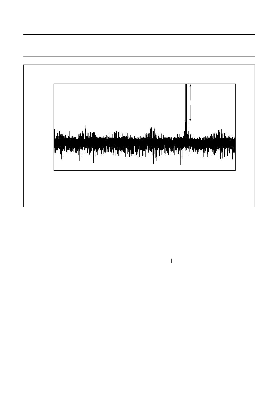
Figure 13 shows the spectrum of a full-scale input sine
wave with frequency f
t
, conforming to coherent sampling
and digitized by the ADC under test.
Coherent sampling means that
, where M is the
number of cycles, N the number of samples and both M
and N being a relative prime.
Remark: the parameter P
noise
used in the following
equations includes the power of the random noise,
non-linearities, sampling time errors and quantization
noise.
INL i
( )
V
in
i
( )
V
in
ideal
(
)
≠
S
----------------------------------------------
=
DNL i
( )
V
in
i
1
+
(
)
V
in
i
( )
≠
S
---------------------------------------------
1
≠
=
f
t
f
s
----
M
N
-----
=
2003 Apr 07
20
Philips Semiconductors
Objective specification
12-bit, 80/105 Msps Analog-to-Digital
Converter (ADC) Nyquist/High IF sampling
TDA8769
handbook, full pagewidth
MBL882
0
0
measured output range (MHz)
2.5
magnitude
-
20
-
40
-
60
-
80
-
100
-
120
-
160
5
7.5
10
12.5
15
17.5
20
22.5
25
27
-
140
IMD3
Fig.13 Spectrum of a full-scale input sine wave with frequency f
t
.
11.5.2.1
Signal-to-noise and distortion, SINAD
SINAD is the ratio of the signal power to the noise plus
distortion power, excluding the DC component, at a given
sample rate and input frequency:
dB.
11.5.2.2
Effective number of bits, ENOB
ENOB is derived from SINAD and gives the theoretical
resolution an ideal ADC would require to obtain the same
SINAD measured on the actual ADC. A good
approximation is:
, where SINAD is expressed in
dB.
11.5.2.3
Total harmonic distortion, THD
THD is the ratio of the power of the harmonics to the power
of the signal frequency. The equation for k
- 1
harmonics
is:
dB, where
Usually THD is calculated with the first five harmonics, or
for k = 6.
11.5.2.4
Signal-to-noise ratio, SNR
SNR is the ratio of the signal power to the noise power,
excluding the harmonics and DC component of the signal:
dB
SINAD
10
P
signal
P
noise + distortion
--------------------------------------
log
=
ENOB
SINAD
1.76
≠
6.02
-------------------------------------
=
THD
10
P
harmonics
P
signal
-------------------------
log
=
P
harmonics
a
2
2
a
3
2
...
a
k
2
+
+
+
=
P
signal
a
1
2
=
SNR
10
P
signal
P
noise
----------------
log
=

2003 Apr 07
21
Philips Semiconductors
Objective specification
12-bit, 80/105 Msps Analog-to-Digital
Converter (ADC) Nyquist/High IF sampling
TDA8769
11.5.2.5
Spurious free dynamic range, SFDR
The SFDR specifies the available signal range as the
spectral distance between the amplitude of the
fundamental and the amplitude of the largest spurious
signal, harmonic and non-harmonic, excluding the
DC component.
dB
11.5.3
I
NTERMODULATION PARAMETERS
,
DUAL TONE
11.5.3.1
Spectral analysis (dual tone)
Figure 14 shows the spectral analysis of a dual tone sine
wave input, at frequencies f
t1
and f
t2
, meeting the
coherence criterion
11.5.3.2
Intermodulation distortion, IMD2 and IMD3
The 2nd and 3rd order intermodulation distortion products,
IMD2 and IMD3 respectively, are defined with a dual tone
input. IMD2 is defined as the ratio of the RMS value of
either tone to the RMS value of the second order
intermodulation product, IMD3 with the third order
intermodulation product. The IMD2 is given by:
dB, where
.
.
and
is the power of the intermodulation
component at f
t
.
11.5.4
N
OISE POWER RATIO
When using a notch filtered broadband white noise
generator as input to the ADC under test, the noise power
ratio is defined as the ratio of the average out-of-notch to
the in-notch power spectral density magnitudes for the
FFT spectrum of the ADC output sample set.
SFDR
10
a
1
max s
( )
--------------------
log
=
IMD2
10
P
intermod
P
signal
---------------------
log
=
P
intermod
a
im
2
f
t1
f
t2
≠
(
)
a
im
2
f
t1
f
t2
+
(
)
≠
a
im
2
f
t1
2f
t2
≠
(
)
+
=
+a
im
2
f
t1
2f
t2
+
(
)
a
im
2
2f
t1
f
t2
≠
(
)
a
im
2
2f
t1
f
t2
+
(
)
+
+
P
signal
a
2
f
t1
( )
a
2
f
t2
( )
+
=
a
im
2
f
t
( )
handbook, full pagewidth
MBL883
measured output range (MHz)
magnitude
SFDR
a2
a3
ak
a1
Fig.14 Spectral analysis with dual tone.
2003 Apr 07
22
Philips Semiconductors
Objective specification
12-bit, 80/105 Msps Analog-to-Digital
Converter (ADC) Nyquist/High IF sampling
TDA8769
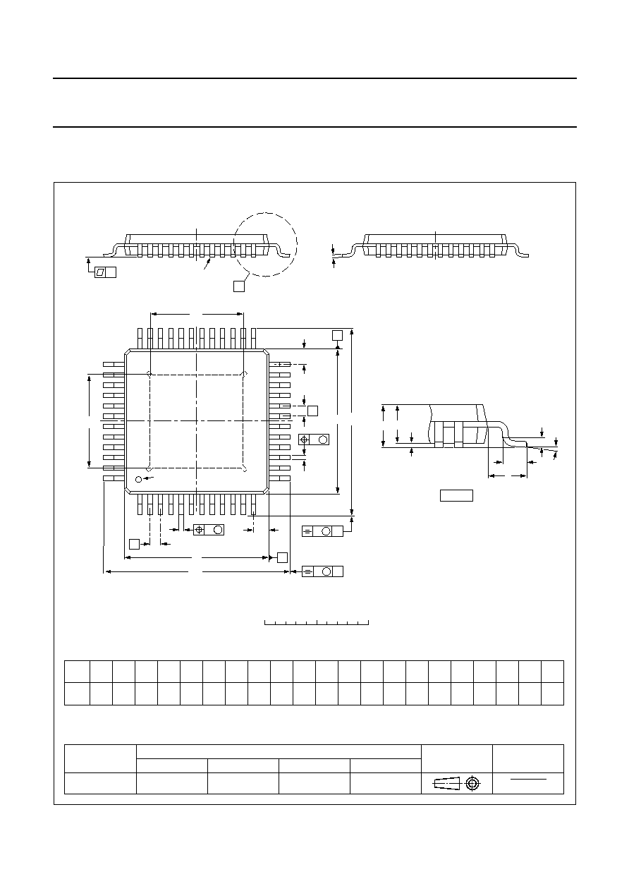
12 PACKAGE OUTLINE
UNIT
A
max.
A1
A2
A3
bp
HD
HE
Lp
ZD
(1)
ZE
(1)
c
e
L
y
w
v
REFERENCES
OUTLINE
VERSION
EUROPEAN
PROJECTION
ISSUE DATE
IEC
JEDEC
JEITA
mm
1.2
0.15
0.05
1.05
0.95
0.25
0.27
0.17
0.20
0.09
7.1
6.9
0.5
9.1
8.9
0.89
0.61
7
∞
0
∞
0.08
0.08
0.2
1
DIMENSIONS (mm are the original dimensions)
Note
1. Plastic or metal protrusions of 0.25 mm maximum per side are not included.
0.75
0.45
SOT545-2
99-08-04
03-04-07
D
(1)
E
(1)
7.1
6.9
9.1
8.9
Dh
Eh
4.6
4.4
4.6
4.4
0.89
0.61
b
p
e
E
A
1
A
L
p
detail X
L
B
12
1
48
37
D
H
b
p
E
H
A
2
v
M
B
D
ZD
A
c
Z E
e
v
M
A
X
25
36
24
13
y
pin 1 index
w
M
w
M
0
2.5
5 mm
scale
HTQFP48: plastic thermal enhanced thin quad flat package; 48 leads;
body 7 x 7 x 1 mm; exposed die pad
SOT545-2
Dh
Eh
exposed die pad side
(A )
3

2003 Apr 07
23
Philips Semiconductors
Objective specification
12-bit, 80/105 Msps Analog-to-Digital
Converter (ADC) Nyquist/High IF sampling
TDA8769
13 SOLDERING
13.1
Introduction to soldering surface mount
packages
This text gives a very brief insight to a complex technology.
A more in-depth account of soldering ICs can be found in
our
"Data Handbook IC26; Integrated Circuit Packages"
(document order number 9398 652 90011).
There is no soldering method that is ideal for all surface
mount IC packages. Wave soldering can still be used for
certain surface mount ICs, but it is not suitable for fine pitch
SMDs. In these situations reflow soldering is
recommended.
13.2
Reflow soldering
Reflow soldering requires solder paste (a suspension of
fine solder particles, flux and binding agent) to be applied
to the printed-circuit board by screen printing, stencilling or
pressure-syringe dispensing before package placement.
Several methods exist for reflowing; for example,
convection or convection/infrared heating in a conveyor
type oven. Throughput times (preheating, soldering and
cooling) vary between 100 and 200 seconds depending
on heating method.
Typical reflow peak temperatures range from
215 to 250
∞
C. The top-surface temperature of the
packages should preferably be kept:
∑
below 220
∞
C for all the BGA packages and packages
with a thickness
2.5 mm and packages with a
thickness <2.5 mm and a volume
350 mm
3
so called
thick/large packages
∑
below 235
∞
C for packages with a thickness <2.5 mm
and a volume <350 mm
3
so called small/thin packages.
13.3
Wave soldering
Conventional single wave soldering is not recommended
for surface mount devices (SMDs) or printed-circuit boards
with a high component density, as solder bridging and
non-wetting can present major problems.
To overcome these problems the double-wave soldering
method was specifically developed.
If wave soldering is used the following conditions must be
observed for optimal results:
∑
Use a double-wave soldering method comprising a
turbulent wave with high upward pressure followed by a
smooth laminar wave.
∑
For packages with leads on two sides and a pitch (e):
≠ larger than or equal to 1.27 mm, the footprint
longitudinal axis is preferred to be parallel to the
transport direction of the printed-circuit board;
≠ smaller than 1.27 mm, the footprint longitudinal axis
must be parallel to the transport direction of the
printed-circuit board.
The footprint must incorporate solder thieves at the
downstream end.
∑
For packages with leads on four sides, the footprint must
be placed at a 45
∞
angle to the transport direction of the
printed-circuit board. The footprint must incorporate
solder thieves downstream and at the side corners.
During placement and before soldering, the package must
be fixed with a droplet of adhesive. The adhesive can be
applied by screen printing, pin transfer or syringe
dispensing. The package can be soldered after the
adhesive is cured.
Typical dwell time is 4 seconds at 250
∞
C.
A mildly-activated flux will eliminate the need for removal
of corrosive residues in most applications.
13.4
Manual soldering
Fix the component by first soldering two
diagonally-opposite end leads. Use a low voltage (24 V or
less) soldering iron applied to the flat part of the lead.
Contact time must be limited to 10 seconds at up to
300
∞
C.
When using a dedicated tool, all other leads can be
soldered in one operation within 2 to 5 seconds between
270 and 320
∞
C.

2003 Apr 07
24
Philips Semiconductors
Objective specification
12-bit, 80/105 Msps Analog-to-Digital
Converter (ADC) Nyquist/High IF sampling
TDA8769
13.5
Suitability of surface mount IC packages for wave and reflow soldering methods
Notes
1. For more detailed information on the BGA packages refer to the
"(LF)BGA Application Note" (AN01026); order a copy
from your Philips Semiconductors sales office.
2. All surface mount (SMD) packages are moisture sensitive. Depending upon the moisture content, the maximum
temperature (with respect to time) and body size of the package, there is a risk that internal or external package
cracks may occur due to vaporization of the moisture in them (the so called popcorn effect). For details, refer to the
Drypack information in the
"Data Handbook IC26; Integrated Circuit Packages; Section: Packing Methods".
3. These packages are not suitable for wave soldering. On versions with the heatsink on the bottom side, the solder
cannot penetrate between the printed-circuit board and the heatsink. On versions with the heatsink on the top side,
the solder might be deposited on the heatsink surface.
4. If wave soldering is considered, then the package must be placed at a 45
∞
angle to the solder wave direction.
The package footprint must incorporate solder thieves downstream and at the side corners.
5. Wave soldering is suitable for LQFP, TQFP and QFP packages with a pitch (e) larger than 0.8 mm; it is definitely not
suitable for packages with a pitch (e) equal to or smaller than 0.65 mm.
6. Wave soldering is suitable for SSOP, TSSOP, VSO and VSSOP packages with a pitch (e) equal to or larger than
0.65 mm; it is definitely not suitable for packages with a pitch (e) equal to or smaller than 0.5 mm.
PACKAGE
(1)
SOLDERING METHOD
WAVE
REFLOW
(2)
BGA, LBGA, LFBGA, SQFP, TFBGA, VFBGA
not suitable
suitable
DHVQFN, HBCC, HBGA, HLQFP, HSQFP, HSOP, HTQFP,
HTSSOP, HVQFN, HVSON, SMS
not suitable
(3)
suitable
PLCC
(4)
, SO, SOJ
suitable
suitable
LQFP, QFP, TQFP
not recommended
(4)(5)
suitable
SSOP, TSSOP, VSO, VSSOP
not recommended
(6)
suitable

2003 Apr 07
25
Philips Semiconductors
Objective specification
12-bit, 80/105 Msps Analog-to-Digital
Converter (ADC) Nyquist/High IF sampling
TDA8769
14 DATA SHEET STATUS
Notes
1. Please consult the most recently issued data sheet before initiating or completing a design.
2. The product status of the device(s) described in this data sheet may have changed since this data sheet was
published. The latest information is available on the Internet at URL http://www.semiconductors.philips.com.
3. For data sheets describing multiple type numbers, the highest-level product status determines the data sheet status.
LEVEL
DATA SHEET
STATUS
(1)
PRODUCT
STATUS
(2)(3)
DEFINITION
I
Objective data
Development
This data sheet contains data from the objective specification for product
development. Philips Semiconductors reserves the right to change the
specification in any manner without notice.
II
Preliminary data Qualification
This data sheet contains data from the preliminary specification.
Supplementary data will be published at a later date. Philips
Semiconductors reserves the right to change the specification without
notice, in order to improve the design and supply the best possible
product.
III
Product data
Production
This data sheet contains data from the product specification. Philips
Semiconductors reserves the right to make changes at any time in order
to improve the design, manufacturing and supply. Relevant changes will
be communicated via a Customer Product/Process Change Notification
(CPCN).
15 DEFINITIONS
Short-form specification
The data in a short-form
specification is extracted from a full data sheet with the
same type number and title. For detailed information see
the relevant data sheet or data handbook.
Limiting values definition
Limiting values given are in
accordance with the Absolute Maximum Rating System
(IEC 60134). Stress above one or more of the limiting
values may cause permanent damage to the device.
These are stress ratings only and operation of the device
at these or at any other conditions above those given in the
Characteristics sections of the specification is not implied.
Exposure to limiting values for extended periods may
affect device reliability.
Application information
Applications that are
described herein for any of these products are for
illustrative purposes only. Philips Semiconductors make
no representation or warranty that such applications will be
suitable for the specified use without further testing or
modification.
16 DISCLAIMERS
Life support applications
These products are not
designed for use in life support appliances, devices, or
systems where malfunction of these products can
reasonably be expected to result in personal injury. Philips
Semiconductors customers using or selling these products
for use in such applications do so at their own risk and
agree to fully indemnify Philips Semiconductors for any
damages resulting from such application.
Right to make changes
Philips Semiconductors
reserves the right to make changes in the products -
including circuits, standard cells, and/or software -
described or contained herein in order to improve design
and/or performance. When the product is in full production
(status `Production'), relevant changes will be
communicated via a Customer Product/Process Change
Notification (CPCN). Philips Semiconductors assumes no
responsibility or liability for the use of any of these
products, conveys no licence or title under any patent,
copyright, or mask work right to these products, and
makes no representations or warranties that these
products are free from patent, copyright, or mask work
right infringement, unless otherwise specified.

2003 Apr 07
26
Philips Semiconductors
Objective specification
12-bit, 80/105 Msps Analog-to-Digital
Converter (ADC) Nyquist/High IF sampling
TDA8769
NOTES

2003 Apr 07
27
Philips Semiconductors
Objective specification
12-bit, 80/105 Msps Analog-to-Digital
Converter (ADC) Nyquist/High IF sampling
TDA8769
NOTES

© Koninklijke Philips Electronics N.V. 2003
SCA75
All rights are reserved. Reproduction in whole or in part is prohibited without the prior written consent of the copyright owner.
The information presented in this document does not form part of any quotation or contract, is believed to be accurate and reliable and may be changed
without notice. No liability will be accepted by the publisher for any consequence of its use. Publication thereof does not convey nor imply any license
under patent- or other industrial or intellectual property rights.
Philips Semiconductors ≠ a worldwide company
Contact information
For additional information please visit http://www.semiconductors.philips.com.
Fax: +31 40 27 24825
For sales offices addresses send e-mail to: sales.addresses@www.semiconductors.philips.com.
Printed in The Netherlands
753504/01/pp
28
Date of release:
2003 Apr 07
Document order number:
9397 750 10843