1998 Dec 01
2
Philips Semiconductors
Preliminary specification
2
◊
50 W class-D power amplifier
TDA8920
FEATURES
∑
High efficiency (90%)
∑
Operating voltage from
±
15 V to
±
30 V
∑
Very low quiescent current
∑
Low distortion
∑
Fixed gain of 30 dB
∑
High output power
∑
Output power limiter
∑
Good ripple rejection
∑
Usable as a mono amplifier in Bridge-Tied Load (BTL) or
as a stereo Single-Ended (SE) amplifier
∑
Tracking possibility for oscillator frequency
∑
Differential audio inputs
∑
No switch-on or switch-off plops
∑
Short-circuit proof across the load
∑
Electrostatic discharge protection on all pins
∑
Thermally protected.
APPLICATIONS
∑
Television sets
∑
Home-sound systems
∑
Multimedia systems.
GENERAL DESCRIPTION
The TDA8920 is a high efficiency class-D audio power
amplifier. It can be used in a mono Bridge-Tied Load (BTL)
or in a stereo Single-Ended (SE) configuration. The device
operates over a wide supply voltage range from
±
15 V up to
±
30 V and consumes a very low quiescent
current.
QUICK REFERENCE DATA
SYMBOL
PARAMETER
CONDITIONS
MIN.
TYP.
MAX.
UNIT
General
V
DD
operating supply voltage
±
15
±
25
±
30
V
I
q(tot)
total quiescent current
-
50
60
mA
efficiency
P
o
= 10 W
85
90
-
%
Stereo single-ended configuration
P
o
output power
THD = 10%
tbf
35
-
W
G
v(cl)
closed loop voltage gain
29
30
31
dB
Z
i
input impedance
80
120
-
k
V
n(o)
noise output voltage
-
100
-
µ
V
SVRR
supply voltage ripple rejection
60
-
-
dB
cs
channel separation
50
tbf
-
dB
Mono bridge-tied load configuration
P
o
output power
THD = 10%
-
130
-
W
G
v(cl)
closed loop voltage gain
35
36
37
dB
Z
i
input impedance
40
60
-
k
V
n(o)
noise output voltage
-
140
-
µ
V
SVRR
supply voltage ripple rejection
66
-
-
dB
V
O
DC output offset voltage
-
-
50
mV
1998 Dec 01
4
Philips Semiconductors
Preliminary specification
2
◊
50 W class-D power amplifier
TDA8920
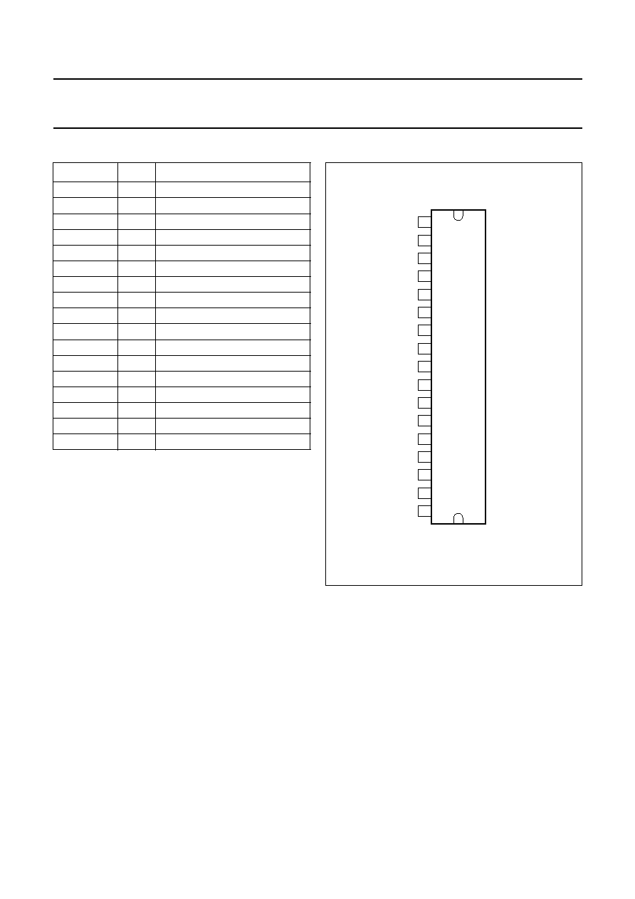
PINNING
Note
1. The case of the package is connected to pins 8 and 10
(V
SS1
and V
SS2
). Therefore no other voltage than V
SS
should be connected to the case or the heatsink.
SYMBOL
PIN
DESCRIPTION
OSC
1
oscillator frequency adjustment
SGND
2
signal ground (0 V)
IN1
-
3
negative input channel 1
IN1+
4
positive input channel 1
V
DD1
5
positive supply voltage 1
BOOT1
6
bootstrapping capacitor 1
OUT1
7
output 1
V
SS1
8
negative supply voltage 1; note 1
STAB
9
internal stabilizer decoupling
V
SS2
10
negative supply voltage 2; note 1
OUT2
11
output 2
BOOT2
12
bootstrapping capacitor 2
V
DD2
13
positive supply voltage 2
IN2+
14
positive input channel 2
IN2
-
15
negative input channel 2
LIM
16
current limiting adjustment
MODE
17
mode select input
Fig.2 Pin configuration (SOT243-1).
handbook, halfpage
TDA8920J
MGR658
OSC
SGND
IN1
-
IN1
+
VDD1
BOOT1
OUT1
VSS1
STAB
VSS2
OUT2
BOOT2
VDD2
IN2
+
IN2
-
LIM
MODE
1
2
3
4
5
6
7
8
9
10
11
12
13
14
15
16
17
1998 Dec 01
5
Philips Semiconductors
Preliminary specification
2
◊
50 W class-D power amplifier
TDA8920
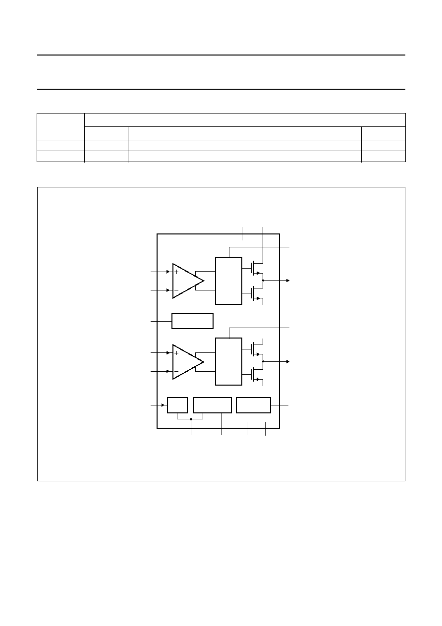
FUNCTIONAL DESCRIPTION
The TDA8920 is a multi purpose audio power amplifier in
class-D technology. It contains two independent amplifiers
with high output power, high efficiency (90%), low
distortion and a low quiescent current. The amplifiers can
be connected in the following configurations:
∑
Mono bridge-tied load amplifier
∑
Stereo single-ended amplifiers.
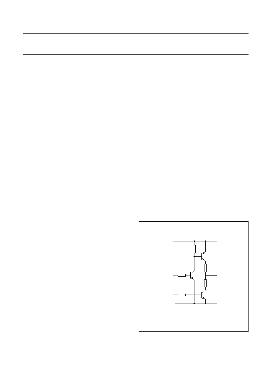
The amplifier can be switched in three operating modes
with the mode select input:
∑
Standby mode, with a very low supply current
(practically zero)
∑
Mute mode; the amplifiers are operational but the audio
signal at the output is suppressed
∑
Operating mode (amplifier fully operational) with output
signal.
For suppressing plop noise the amplifier will remain
automatically for approximately 500 ms in the mute
mode before switching to operating mode. During this
time the coupling capacitors at the input are fully
charged. An example of a switching circuit for driving the
mode select input is illustrated in Fig.3.
Pulse Width Modulation (PWM) frequency
The output signal of the amplifier is a PWM signal with a
sample frequency of 500 kHz. The use of a second order
LC filter in the application results in an analog audio signal
across the loudspeaker. This switching frequency is fixed
by an external resistor R
OSC
connected between pin OSC
and pin SGND. With the resistor value given in the
application diagram, the oscillating frequency is typical
500 kHz. The oscillator frequency can be calculated using:
If two or more devices are used in the same audio system
it is advised to have both devices working on the same
oscillation frequency. This can be realized by connecting
all OSC pins together.
f
osc
5.10
9
R
OSC
-------------- Hz
[
]
=
Current limiting
With an external resistor R
LIM
connected between pin LIM
and V
SS
the maximum output current of the amplifiers can
be set. If pin LIM is short-circuited to V
SS
, then the
maximum output current is limited to 7 A. The relationship
between maximum output current and resistor value is
given by:
Protections
Protections are included to avoid the device being
damaged at:
∑
Over-temperature T
j
> 150
∞
C
∑
Short-circuit of the loudspeaker terminals: when
short-circuited the power dissipation is limited
∑
A maximum current limiter which limits the maximum
output current to 7 A, or to the value set by R
LIM
. During
limiting the current is measured and when the current is
higher than 7 A, the amplifier is switched off within 3
µ
s
and every 20 ms the IC tries to restart. The dissipation
will be low because of this low duty cycle.
∑
ESD protection (human body model: 3000 V and
machine model: 300 V).
I
O(max)
70.10
3
10.10
3
R
LIM
+
------------------------------------------- A
[ ]
=
Fig.3 Mode select input drive circuit.
handbook, halfpage
MGR660
R
pin MODE
SGND
R
+
5 V
standby/on
mute