 | –≠–ª–µ–∫—Ç—Ä–æ–Ω–Ω—ã–π –∫–æ–º–ø–æ–Ω–µ–Ω—Ç: TDA9183P | –°–∫–∞—á–∞—Ç—å:  PDF PDF  ZIP ZIP |
Document Outline
- FEATURES
- GENERAL DESCRIPTION
- QUICK REFERENCE DATA
- ORDERING INFORMATION
- BLOCK DIAGRAM
- PINNING
- FUNCTIONAL DESCRIPTION
- Input configuration
- Comb filter
- Output configuration
- Clock generation and filter tuning
- Mode definitions
- LIMITING VALUES
- THERMAL CHARACTERISTICS
- CHARACTERISTICS
- APPLICATION INFORMATION
- PACKAGE OUTLINES
- SOLDERING
- DATA SHEET STATUS
- DEFINITIONS
- DISCLAIMERS

DATA SHEET
Objective specification
Supersedes data of 2000 Nov 22
File under Integrated Circuits, IC02
2000 Nov 30
INTEGRATED CIRCUITS
TDA9183
Integrated NTSC comb filter

2000 Nov 30
2
Philips Semiconductors
Objective specification
Integrated NTSC comb filter
TDA9183
FEATURES
∑
One-chip NTSC adaptive comb filter
∑
Cross luminance reduction
∑
Cross colour reduction
∑
No chroma trap, therefore sharper vertical luminance
transients
∑
Analog discrete-time signal processing, therefore no
quantization noise
∑
Anti-aliasing and reconstruction filters are included
∑
Input switch selects between two Y/CVBS inputs
∑
Output switch selects between combed CVBS and an
external Y/C source
∑
f
SC
as well as 2
◊
f
SC
colour subcarrier signal may be
applied
∑
Alignment free
∑
Few external components
∑
Low power.
GENERAL DESCRIPTION
The TDA9183 is a an adaptive NTSC comb filter with two
internal delay lines, filters, clock control and input clamps.
The NTSC M video standard is supported.
Two CVBS input signals can be selected by means of an
input switch.
The selected CVBS input signal is filtered to obtain
a combed luminance output signal and a combed
chrominance output signal. Switched capacitor circuit
techniques are used, requiring an internal clock, locked on
to the colour subcarrier frequency.
The colour subcarrier frequency as well as twice the colour
subcarrier frequency may be applied to the IC.
In addition to the comb filter the circuit contains an output
switch so that a selection can be made between the
combed CVBS signal and an external Y/C signal.
The IC is available in a DIP16 and SO16 package.
The supply voltage is 5 V.
QUICK REFERENCE DATA
ORDERING INFORMATION
SYMBOL
PARAMETER
MIN.
TYP.
MAX.
UNIT
V
CCA
analog supply voltage
4.5
5.0
5.5
V
I
CCA
analog supply current
-
25
-
mA
V
DDD
digital supply voltage
4.5
5.0
5.5
V
I
DDD
digital supply current
-
10
-
mA
V
i(Y/CVBS)(p-p)
luminance or CVBS input signal voltage (peak-to-peak value)
0.7
1.0
1.4
V
V
i(CIN)(p-p)
chrominance input signal voltage (peak-to-peak value)
-
0.7
1.0
V
V
i(FSC)(p-p)
colour subcarrier input signal voltage (peak-to-peak value)
100
200
400
mV
V
o(Y/CVBS)(p-p)
luminance or CVBS output signal voltage (peak-to-peak value)
0.6
1.0
1.54
V
V
o(CIN)(p-p)
chrominance output signal voltage (peak-to-peak value)
-
0.7
1.1
V
TYPE
NUMBER
PACKAGE
NAME
DESCRIPTION
VERSION
TDA9183P
DIP16
plastic dual in-line package; 16 leads (300 mil); long body
SOT38-4
TDA9183T
SO16
plastic small outline package; 16 leads; body width 7.5 mm
SOT162-1
2000
Nov
30
3
Philips Semiconductors
Objectiv
e specification
Integ
r
ated NTSC comb filter
TD
A9183
This text is here in white to force landscape pages to be rotated correctly when browsing through the pdf in the Acrobat reader.This text is here in
_
white to force landscape pages to be rotated correctly when browsing through the pdf in the Acrobat reader.This text is here inThis text is here in
white to force landscape pages to be rotated correctly when browsing through the pdf in the Acrobat reader. white to force landscape pages to be ...
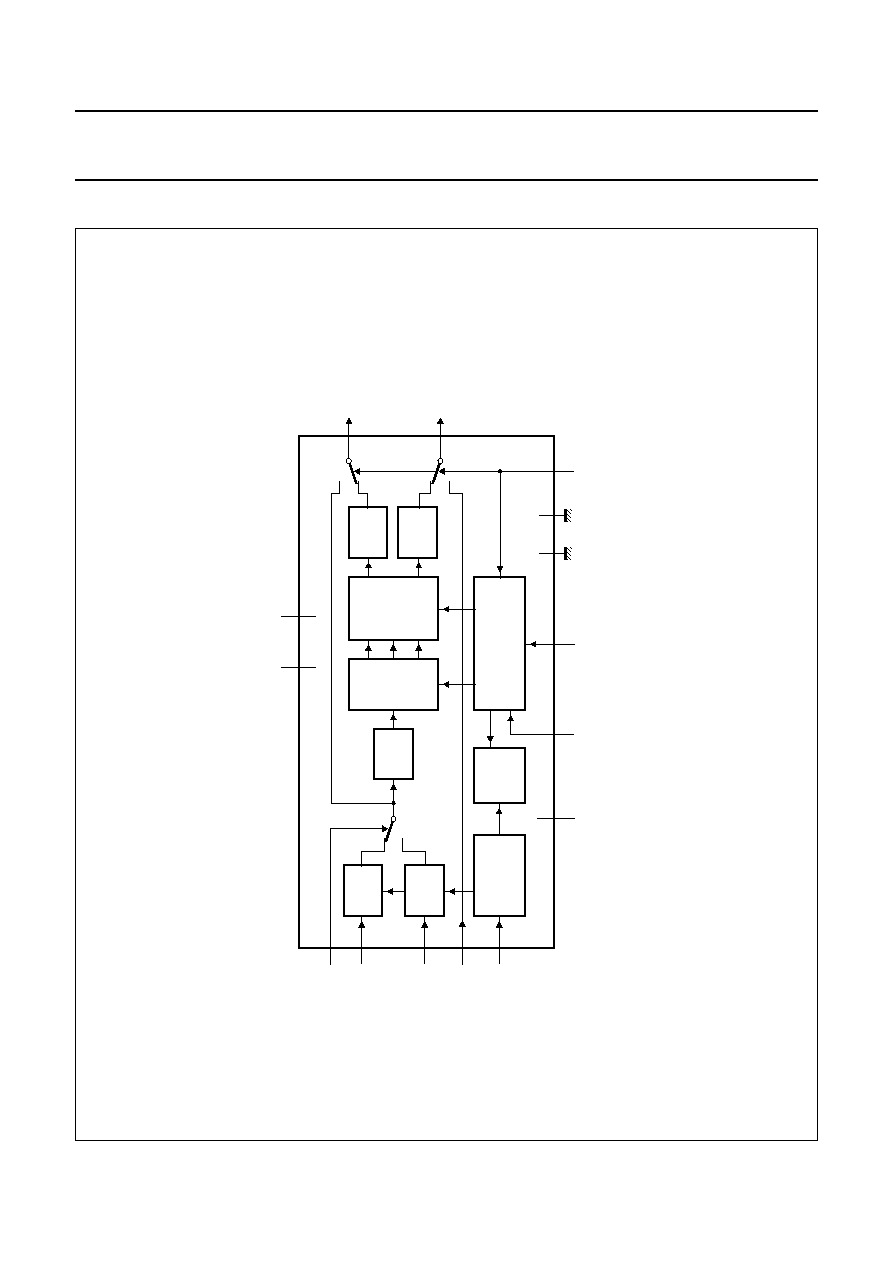
BLOCK DIA
GRAM
handbook, full pagewidth
MGT535
Y/CVBSOUT
COUT
12
9
6
8
14
16
2
FSC
FSCSEL
VCCA
SANDCASTLE
DETECTOR
CLAMP
LPF
LPF
LPF
CLAMP
10, 11
n.c.
15
OUTSEL
13
AGND
4
DGND
2H/4H
DELAY
ADAPTIVE
COMB
FILTER
Y/CVBS1
INPSEL
3
Y/CVBS2
7
FILTER
TUNING
(LPFs)
4
◊
fsc
CLOCK GENERATOR
SC
1
CIN
5
VDDD
TDA9183
Fig.1 Block diagram.

2000 Nov 30
4
Philips Semiconductors
Objective specification
Integrated NTSC comb filter
TDA9183
PINNING
SYMBOL
PIN
DESCRIPTION
C
IN
1
chrominance signal input
INPSEL
2
input switch select input
Y/CVBS
2
3
luminance or CVBS signal 2 input
DGND
4
digital ground
V
DDD
5
digital supply voltage
V
CCA
6
analog supply voltage
SC
7
sandcastle signal input
FSCSEL
8
colour subcarrier select input
FSC
9
colour subcarrier signal input
n.c.
10
not connected
n.c.
11
not connected
Y/CVBS
1
12
luminance or CVBS signal 1 input
AGND
13
analog ground (signal reference)
Y/CVBS
OUT
14
luminance or CVBS signal output
OUTSEL
15
output switch select input
C
OUT
16
chrominance signal output
handbook, halfpage
TDA9183P
MGT536
1
2
3
4
5
6
7
8
16
15
14
13
12
11
10
9
CIN
INPSEL
Y/CVBS2
DGND
VDDD
VCCA
SC
FSCSEL
FSC
n.c.
n.c.
Y/CVBS1
AGND
Y/CVBSOUT
OUTSEL
COUT
Fig.2 Pin configuration (DIP16).
handbook, halfpage
TDA9183T
MGT537
1
2
3
4
5
6
7
8
16
15
14
13
12
11
10
9
CIN
INPSEL
Y/CVBS2
DGND
VDDD
VCCA
SC
FSCSEL
FSC
n.c.
n.c.
Y/CVBS1
AGND
Y/CVBSOUT
OUTSEL
COUT
Fig.3 Pin configuration (SO16).

2000 Nov 30
5
Philips Semiconductors
Objective specification
Integrated NTSC comb filter
TDA9183
FUNCTIONAL DESCRIPTION
Input configuration
The Y/CVBS
1
and Y/CVBS
2
input signals are clamped by
means of an internally generated clamp pulse which is
derived from the sandcastle input signal (pin SC). If no
sandcastle signal is available, a clamp pulse signal may be
applied to pin SC. External clamp capacitors are needed.
The buffered and clamped Y/CVBS
1
and Y/CVBS
2
signals
are then applied to the input switch. The input switch select
signal (INPSEL) determines whether Y/CVBS
1
or
Y/CVBS
2
is passed through to the anti-alias low-pass filter.
This 3rd-order low-pass filter is optimized for best
performance with respect to step response and clock
suppression. The filtered signal is sampled at a clock
frequency of four times the colour subcarrier frequency
(f
SC
).
A colour subcarrier frequency signal is applied to pin FSC.
The colour subcarrier select input signal (FSCSEL)
indicates whether the colour subcarrier frequency (f
SC
) or
twice the colour subcarrier frequency (2
◊
f
SC
) is being
applied at the FSC input. An external coupling capacitor is
needed for the colour subcarrier input signal.
Comb filter
The sampled CVBS signal is applied to two delay lines.
One delay line delays the signal over 1H (1H = one
line-time).
The direct and delayed signals are applied to an adaptive
comb filter. The adaptive comb filter performs band-pass
filtering around the colour subcarrier frequency and
compares the contents of adjacent lines. In this way the
combing of signals with different information is prevented
and artifacts such as hanging dots are avoided.
Both the combed chrominance and the combed luminance
signal are passed through a reconstruction low-pass filter
to obtain continuous-time signals. These low-pass filters
are 3rd-order, optimized for best performance with respect
to step response and clock suppression. The
reconstructed signals are applied to the output switches.
Output configuration
The luminance output switch selects between the
reconstructed combed luminance signal and one of the
buffered and clamped input signals Y/CVBS
1
or Y/CVBS
2
.
The chrominance output switch selects between the
reconstructed combed chrominance signal and the
chrominance input signal (C
IN
). An external coupling
capacitor is needed for C
IN
. The selected signals are
applied to the outputs Y/CVBS
OUT
and C
OUT
respectively
via a buffer stage. The output switch signal (OUTSEL)
determines whether the output switches select the internal
combed signals or the external Y/C signals.
Clock generation and filter tuning
The clock generator is driven by a Phase-Locked Loop
(PLL) circuit which generates a reference frequency of four
times the colour subcarrier frequency. This PLL circuit is
phase-locked to the colour subcarrier input signal (FSC).
Several internal clock signals are derived from the 4
◊
f
SC
reference.
The filter tuning ensures the automatic alignment of the
anti-alias and the reconstruction low-pass filters. A 4
◊
f
SC
clock signal is used as a reference for the alignment. The
tuning takes place each line during the line blanking and is
initiated by means of an internally generated signal which
is derived from the sandcastle input signal.
If the output switches select external Y/C signals the
oscillator of the PLL circuit is stopped regardless of the
FSC input and no internal clock signals are generated. The
filter tuning is also stopped.

2000 Nov 30
6
Philips Semiconductors
Objective specification
Integrated NTSC comb filter
TDA9183
Mode definitions
Table 1
General mode definitions; note 1
Note
1. If the OUTSEL pin is left open-circuit, the pin is pulled
LOW by means of an internal pull-down resistor to
analog ground (AGND). Thus the COMB mode can
also be selected by not connecting the OUTSEL pin.
Table 2
Y/CVBS
OUT
output signal definitions
Table 3
C
OUT
output signal definitions
Table 4
Input switch mode definitions; note 1
Note
1. If the INPSEL pin is left open-circuit, the pin is pulled
LOW by means of an internal pull-down resistor to
analog ground (AGND). Thus the Y/CVBS
1
input can
also be selected by not connecting the INPSEL pin.
Table 5
FSC mode definitions; note 1
Note
1. If the FSCSEL pin is left open-circuit, the pin is pulled
LOW by means of an internal pull-down resistor to
analog ground (AGND). Thus the f
SC
mode can also
be selected by not connecting the FSCSEL pin.
PIN OUTSEL
MODE
LOW
COMB
HIGH
YC
MODE
Y/CVBS
OUT
OUTPUT SIGNAL
COMB
comb filtered luminance signal
YC
Y/CVBS
1
or Y/CVBS
2
signal
MODE
C
OUT
OUTPUT SIGNAL
COMB
comb filtered chrominance signal
YC
C
IN
signal
PIN INPSEL
INPUT SWITCH MODE
LOW
Y/CVBS
1
input selected
HIGH
Y/CVBS
2
input selected
PIN FSCSEL
FSC INPUT SIGNAL FREQUENCY
LOW
f
SC
HIGH
2
◊
f
SC
2000 Nov 30
7
Philips Semiconductors
Objective specification
Integrated NTSC comb filter
TDA9183
LIMITING VALUES
In accordance with the Absolute Maximum Rating System (IEC 60134).
Notes
1. All pins are protected against ESD by means of internal clamping diodes.
2. Human Body Model (HBM): R = 1.5 k
; C = 100 pF.
3. Pins 5 (V
DDD
) and 6 (V
CCA
): HBM:
-
1500 V < V
es
< +1500 V.
4. Machine Model (MM): R = 0
; C = 200 pF.
5. Pins 5 (V
DDD
) and 6 (V
CCA
): MM:
-
150 V < V
es
< +150 V.
THERMAL CHARACTERISTICS
QUALITY SPECIFICATION
In accordance with
"SNW-FQ-611E".
Latch-up
At an ambient temperature of 70
∞
C all pins meet the following specification:
∑
I
trigger
100 mA or V
trigger
1.5V
DD(max)
∑
I
trigger
-
100 mA or V
trigger
-
0.5V
DD(max)
.
SYMBOL
PARAMETER
CONDITIONS
MIN.
MAX.
UNIT
V
DDD
digital supply voltage
-
5.5
V
V
CCA
analog supply voltage
-
5.5
V
V
i(prot)(th)
input voltage protection threshold
-
0.3
V
DD
+ 0.3
V
T
stg
storage temperature
-
25
+150
∞
C
T
amb
ambient temperature
-
25
+70
∞
C
T
sol
soldering temperature
for 5 s
-
260
∞
C
T
j
junction temperature
-
150
∞
C
V
es
electrostatic handling voltage
HBM; all pins, except
pins 5 and 6; notes 1, 2 and 3
-
3000
+3000
V
MM; all pins, except
pins 5 and 6; notes 1, 4 and 5
-
300
+300
V
SYMBOL
PARAMETER
CONDITIONS
VALUE
UNIT
R
th(j-a)
thermal resistance from junction to ambient in free air
TDA9183P
75
K/W
TDA9183T
95
K/W
2000 Nov 30
8
Philips Semiconductors
Objective specification
Integrated NTSC comb filter
TDA9183
CHARACTERISTICS
V
CCA
= V
DDD
= 5 V; T
amb
= 25
∞
C; input signal Y/CVBS
1
= 1 V (p-p); input signal Y/CVBS
2
= 1 V (p-p); input signal
C
IN
= 0.7 V (p-p); input signal FSC = 200 mV (p-p) sine wave at f
SC
; input signal SC = 5 V (p-p) sandcastle signal; test
signal: 100% white 75% amplitude FCC colour bar; source impedance for Y/CVBS
1
and Y/CVBS = 75
; coupled with
10 nF; source impedance for C
IN
and FSC = 75
; coupled with 100 nF; load impedance for CVBS/Y
OUT
and
C
OUT
= 15 pF to analog ground (pin AGND); all voltages are related to analog ground (pin AGND); unless otherwise
specified.
SYMBOL
PARAMETER
CONDITIONS
MIN.
TYP.
MAX.
UNIT
Supplies
V
CCA
analog supply voltage
4.5
5.0
5.5
V
I
CCA
analog supply current
-
25
-
mA
V
DDD
digital supply voltage
4.5
5.0
5.5
V
I
DDD
digital supply current
-
10
-
mA
P
power dissipation
-
175
-
mW
Luminance or CVBS input 1 and 2; pins Y/CVBS
1
and Y/CVBS
2
V
i(Y/CVBS)(p-p)
luminance or CVBS input
voltage (peak-to-peak value)
including sync
0.7
1.0
1.4
V
t
clamp(Y/CVBS)
clamp time constant
-
20
-
lines
I
i(Y/CVBS)
input current
during clamping
-
10
0
+10
µ
A
during active video
-
10
0
+10
nA
Chrominance input; pin C
IN
V
i(CIN)(p-p)
chrominance input voltage
(peak-to-peak value)
-
0.7
1.0
V
R
i(CIN)
input resistance
30
-
-
k
Colour subcarrier input; pin FSC
V
i(FSC)(p-p)
subcarrier input voltage
(peak-to-peak value)
100
200
400
mV
D
duty cycle
square wave
40
50
60
%
R
i(FSC)
input resistance
30
-
-
k
Sandcastle input; pin SC
V
i(SC)
sandcastle input voltage
no clamping
-
-
3.3
V
clamping
3.7
-
-
V
t
W
pulse width
clamping; note 1
2.6
-
-
µ
s
t
W(rep)
input pulse rising edge
position
with respect to the end
of line blanking; note 1
-
-
-
2.6
µ
s
R
i(SC)
input resistance
1
-
-
M
C
i(SC)
input capacitance
-
-
2
pF
Input switch select input; pin INPSEL
V
IL
LOW-level input voltage
Y/CVBS
1
selected
-
-
0.5
V
V
IH
HIGH-level input voltage
Y/CVBS
2
selected
2.0
-
-
V
R
i(INPSEL)
input resistance
100
-
-
k
C
i(INPSEL)
input capacitance
-
-
2
pF
2000 Nov 30
9
Philips Semiconductors
Objective specification
Integrated NTSC comb filter
TDA9183
Output switch select input; pin OUTSEL
V
IL
LOW-level input voltage
COMB mode
-
-
0.5
V
V
IH
HIGH-level input voltage
YC mode
2.0
-
-
V
R
i(OUTSEL)
input resistance
100
-
-
k
C
i(OUTSEL)
input capacitance
-
-
2
pF
Colour subcarrier select input; pin FSCSEL
V
IL
LOW-level input voltage
f
SC
at FSC input; note 2
-
-
0.5
V
V
IH
HIGH-level input voltage
2
◊
f
SC
at FSC input
2.0
-
-
V
R
i(FSCSEL)
input resistance
100
-
-
k
C
i(FSCSEL)
input capacitance
-
-
2
pF
Luminance output; pin Y/CVBS
OUT
V
o(Y/CVBSOUT)(p-p)
luminance output signal
(peak-to-peak value)
including sync
0.6
1.0
1.54
V
E
G(Y)
luminance gain error
-
1
0
+1
dB
B
-
3dB(Y)
-
3 dB luminance bandwidth
COMB mode
5
-
-
MHz
YC mode
10
-
-
MHz
t
d(proc)(Y)
luminance processing delay
COMB mode; note 3
-
800
-
ns
YC mode
-
15
-
ns
V
clamp
voltage level during
clamping
-
1.5
-
V
E
bl
black level error
during blanking; note 4
-
10
0
+10
mV
S/N
luminance signal-to-noise
ratio (1 V/V
rms
noise)
unweighted; 200 kHz to
5 MHz
56
-
-
dB
ct
crosstalk between different
inputs
0 to 5 MHz
-
-
-
50
dB
f
clk(res)(Y)
residues of clock
frequencies in the luminance
signal (V
rms
/1 V)
COMB mode; note 2
f = 4
◊
f
SC
-
-
-
30
dB
f = 2
◊
f
SC
-
-
-
30
dB
f = 1.33
◊
f
SC
-
-
-
30
dB
f = f
SC
-
-
-
40
dB
FSC
res(YC)
FSC residue in YC mode
(V
rms
/1 V)
f = f
SC
; f
SC
at FSC
input; note 2
-
-
-
60
dB
f = 2
◊
f
SC
; 2
◊
f
SC
at
FSC input
-
-
-
60
dB
ct
crosstalk suppression at
vertical transient black
multi-burst (1 V/V (p-p))
vertical transition active
video
vertical
blanking; note 5 and
Fig.5
26
-
-
dB
SYMBOL
PARAMETER
CONDITIONS
MIN.
TYP.
MAX.
UNIT
2000 Nov 30
10
Philips Semiconductors
Objective specification
Integrated NTSC comb filter
TDA9183
SUP
comb(Y)
suppression (comb depth)
with respect to luminance
band-pass nearest to f
SC
COMB mode; note 2
and Fig.6
f = f
SC
30
-
-
dB
-
10
-
dB
-
10
-
dB
R
o
output resistance
-
-
500
Z
L
load impedance
-
-
15
pF
Chrominance output; pin C
OUT
V
o(COUT)(p-p)
chrominance output signal
(peak-to-peak value)
-
0.7
1.1
V
E
G(chrom)
chrominance gain error
-
1
0
+1
dB
B
-
3dB(chrom)
-
3 dB chrominance
bandwidth
COMB mode; around
f
SC
; note 2
1.5
-
-
MHz
YC mode; base-band
10
-
-
MHz
t
(proc)(Y)
difference with luminance
processing delay
-
0
20
ns
V
DC
DC voltage level
-
1.5
-
V
S/N
chrom
chrominance signal-to-noise
ratio (0.7 V/V
rms
noise)
unweighted;
f
SC
±
0.3f
SC
; note 2
56
-
-
dB
ct
crosstalk between different
inputs
0 to 5 MHz
-
-
-
50
dB
f
clk(res)(chrom)
residues of clock
frequencies in the
chrominance signal
(V
rms
/0.7 V)
COMB mode; note 2
f = 4
◊
f
SC
-
-
-
30
dB
f = 2
◊
f
SC
-
-
-
30
dB
f = 1.33
◊
f
SC
-
-
-
40
dB
f = f
SC
-
-
-
50
dB
FSC
res(YC)
FSC residue in YC mode
(V
rms
/0.7 V)
f = f
SC
; f
SC
at FSC input
-
-
-
60
dB
f = 2
◊
f
SC
; 2
◊
f
SC
at
FSC input; note 2
-
-
-
60
dB
ct
crosstalk suppression at
vertical transient no-colour
colour [0.7 V/V (p-p)]
vertical transition active
video
vertical
blanking; note 6
and Fig.5
26
-
-
dB
SYMBOL
PARAMETER
CONDITIONS
MIN.
TYP.
MAX.
UNIT
f
227.5
59
≠
227.5
---------------------------
f
SC
◊
=
f
227.5
59
+
227.5
----------------------------
f
SC
◊
=
2000 Nov 30
11
Philips Semiconductors
Objective specification
Integrated NTSC comb filter
TDA9183
Notes
1. The pulse should fall inside the line-blanking interval, after the rising edge of the synchronizing pulse.
2. f
SC
= colour subcarrier frequency; f
SC
= 3.579545 MHz for the NTSC M system.
3. With respect to 227.5 colour subcarrier periods (equals 63.556
µ
s) due to 1H delay in the comb filter.
4. With respect to the voltage level during clamping.
5. Test signal for NTSC M: 100% amplitude FCC multi-burst (see Fig.4).
6. Test signal for NTSC M: 100% white 75% amplitude FCC colour bar.
SUP
comb(chrom)
suppression (comb depth)
with respect to chrominance
band pass at f = f
SC
COMB mode; note 2
and Fig.7
30
-
-
dB
30
-
-
dB
30
-
-
dB
R
o
output resistance
-
-
500
Z
L
load impedance
-
-
15
pF
SYMBOL
PARAMETER
CONDITIONS
MIN.
TYP.
MAX.
UNIT
f
227
227.5
---------------
f
SC
◊
=
f
227
59
≠
227.5
----------------------
f
SC
◊
=
f
227
59
+
227.5
-----------------------
f
SC
◊
=
handbook, full pagewidth
MGT522
(V)
0.5
1.5
2.0
3.0
3.58
4.1
MHz
1
0
0.30
0.15
0.45
0.65
Fig.4 100% amplitude FCC multi-burst.

2000 Nov 30
12
Philips Semiconductors
Objective specification
Integrated NTSC comb filter
TDA9183
handbook, full pagewidth
MGT524
line n
-
2
input
line n
-
1
line n
+
1
line n
+
2
line n
+
3
line n
line n
-
2
output
line n
-
1
line n
+
1
line n
+
2
line n
+
3
line n
Transition at top of field
crosstalk
crosstalk
line n
-
2
input
line n
-
1
line n
+
1
line n
+
2
line n
+
3
line n
line n
-
2
output
line n
-
1
line n
+
1
line n
+
2
line n
+
3
line n
Transition at bottom of field
Fig.5 Vertical transitions active video
vertical blanking from line to line (NTSC system).
2000 Nov 30
13
Philips Semiconductors
Objective specification
Integrated NTSC comb filter
TDA9183
handbook, full pagewidth
MGT528
1
C
C
C
C
C
Y
Y
0
Detailed view
comb depth at f = fSC
1
◊
fSC 2
◊
fSC
Y
Y
0.5
0
1
0.5
0
226
227.5
fSC
226.5
227.5
fSC
227
227.5
fSC
227.5
227.5
fSC
228
227.5
fSC
228.5
227.5
fSC
229
227.5
fSC
229.5
227.5
fSC
225.5
227.5
fSC
Fig.6 Luminance transfer characteristic (NTSC M system).

2000 Nov 30
14
Philips Semiconductors
Objective specification
Integrated NTSC comb filter
TDA9183
handbook, full pagewidth
MGT532
1
Y
Y
Y
Y
C
C
0
Detailed view
1
◊
fSC 2
◊
fSC
C
C
0.5
0
1
0.5
0
226
227.5
fSC
226.5
227.5
fSC
227
227.5
fSC
227.5
227.5
fSC
comb depth at f =
227
227.5
fSC
228
227.5
fSC
228.5
227.5
fSC
229
227.5
fSC
225.5
227.5
fSC
Fig.7 Chrominance transfer characteristic (NTSC M system).

2000 Nov 30
15
Philips Semiconductors
Objective specification
Integrated NTSC comb filter
TDA9183
APPLICATION INFORMATION
handbook, full pagewidth
MGT538
220
µ
H
100 nF
C1
10 nF
C3
L5
220
µ
H
L6
5 V
100 nF
C4
TDA9183
1
16
2
15
3
14
4
13
5
12
6
11
7
10
8
9
CIN
INPSEL
Y/CVBS2
SC
FSCSEL
FSC
n.c.
n.c.
Y/CVBS1
Y/CVBSOUT
OUTSEL
COUT
10 nF
C12
100 nF
100
nF
C9
C6
Fig.8 Application diagram.
2000 Nov 30
16
Philips Semiconductors
Objective specification
Integrated NTSC comb filter
TDA9183
PACKAGE OUTLINES
REFERENCES
OUTLINE
VERSION
EUROPEAN
PROJECTION
ISSUE DATE
IEC
JEDEC
EIAJ
SOT38-4
92-11-17
95-01-14
M
H
c
(e )
1
M
E
A
L
seating plane
A
1
w
M
b
1
b
2
e
D
A
2
Z
16
1
9
8
E
pin 1 index
b
0
5
10 mm
scale
Note
1. Plastic or metal protrusions of 0.25 mm maximum per side are not included.
UNIT
A
max.
1
2
b
1
(1)
(1)
(1)
b
2
c
D
E
e
M
Z
H
L
mm
DIMENSIONS (inch dimensions are derived from the original mm dimensions)
A
min.
A
max.
b
max.
w
M
E
e
1
1.73
1.30
0.53
0.38
0.36
0.23
19.50
18.55
6.48
6.20
3.60
3.05
0.254
2.54
7.62
8.25
7.80
10.0
8.3
0.76
4.2
0.51
3.2
inches
0.068
0.051
0.021
0.015
0.014
0.009
1.25
0.85
0.049
0.033
0.77
0.73
0.26
0.24
0.14
0.12
0.01
0.10
0.30
0.32
0.31
0.39
0.33
0.030
0.17
0.020
0.13
DIP16: plastic dual in-line package; 16 leads (300 mil)
SOT38-4
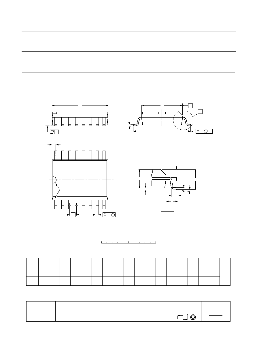
2000 Nov 30
17
Philips Semiconductors
Objective specification
Integrated NTSC comb filter
TDA9183
UNIT
A
max.
A
1
A
2
A
3
b
p
c
D
(1)
E
(1)
(1)
e
H
E
L
L
p
Q
Z
y
w
v
REFERENCES
OUTLINE
VERSION
EUROPEAN
PROJECTION
ISSUE DATE
IEC
JEDEC
EIAJ
mm
inches
2.65
0.30
0.10
2.45
2.25
0.49
0.36
0.32
0.23
10.5
10.1
7.6
7.4
1.27
10.65
10.00
1.1
1.0
0.9
0.4
8
0
o
o
0.25
0.1
DIMENSIONS (inch dimensions are derived from the original mm dimensions)
Note
1. Plastic or metal protrusions of 0.15 mm maximum per side are not included.
1.1
0.4
SOT162-1
8
16
w
M
b
p
D
detail X
Z
e
9
1
y
0.25
075E03
MS-013
pin 1 index
0.10
0.012
0.004
0.096
0.089
0.019
0.014
0.013
0.009
0.41
0.40
0.30
0.29
0.050
1.4
0.055
0.419
0.394
0.043
0.039
0.035
0.016
0.01
0.25
0.01
0.004
0.043
0.016
0.01
X
A
A
1
A
2
H
E
L
p
Q
E
c
L
v
M
A
(A )
3
A
0
5
10 mm
scale
SO16: plastic small outline package; 16 leads; body width 7.5 mm
SOT162-1
97-05-22
99-12-27

2000 Nov 30
18
Philips Semiconductors
Objective specification
Integrated NTSC comb filter
TDA9183
SOLDERING
Introduction
This text gives a very brief insight to a complex technology.
A more in-depth account of soldering ICs can be found in
our
"Data Handbook IC26; Integrated Circuit Packages"
(document order number 9398 652 90011).
There is no soldering method that is ideal for all IC
packages. Wave soldering is often preferred when
through-hole and surface mount components are mixed on
one printed-circuit board. Wave soldering can still be used
for certain surface mount ICs, but it is not suitable for fine
pitch SMDs. In these situations reflow soldering is
recommended.
Through-hole mount packages
S
OLDERING BY DIPPING OR BY SOLDER WAVE
The maximum permissible temperature of the solder is
260
∞
C; solder at this temperature must not be in contact
with the joints for more than 5 seconds. The total contact
time of successive solder waves must not exceed
5 seconds.
The device may be mounted up to the seating plane, but
the temperature of the plastic body must not exceed the
specified maximum storage temperature (T
stg(max)
). If the
printed-circuit board has been pre-heated, forced cooling
may be necessary immediately after soldering to keep the
temperature within the permissible limit.
M
ANUAL SOLDERING
Apply the soldering iron (24 V or less) to the lead(s) of the
package, either below the seating plane or not more than
2 mm above it. If the temperature of the soldering iron bit
is less than 300
∞
C it may remain in contact for up to
10 seconds. If the bit temperature is between
300 and 400
∞
C, contact may be up to 5 seconds.
Surface mount packages
R
EFLOW SOLDERING
Reflow soldering requires solder paste (a suspension of
fine solder particles, flux and binding agent) to be applied
to the printed-circuit board by screen printing, stencilling or
pressure-syringe dispensing before package placement.
Several methods exist for reflowing; for example,
convection or convection/infrared heating in a conveyor
type oven. Throughput times (preheating, soldering and
cooling) vary between 100 and 200 seconds depending
on heating method.
Typical reflow peak temperatures range from
215 to 250
∞
C. The top-surface temperature of the
packages should preferable be kept below 220
∞
C for
thick/large packages, and below 235
∞
C for small/thin
packages.
W
AVE SOLDERING
Conventional single wave soldering is not recommended
for surface mount devices (SMDs) or printed-circuit boards
with a high component density, as solder bridging and
non-wetting can present major problems.
To overcome these problems the double-wave soldering
method was specifically developed.
If wave soldering is used the following conditions must be
observed for optimal results:
∑
Use a double-wave soldering method comprising a
turbulent wave with high upward pressure followed by a
smooth laminar wave.
∑
For packages with leads on two sides and a pitch (e):
≠ larger than or equal to 1.27 mm, the footprint
longitudinal axis is preferred to be parallel to the
transport direction of the printed-circuit board;
≠ smaller than 1.27 mm, the footprint longitudinal axis
must be parallel to the transport direction of the
printed-circuit board.
The footprint must incorporate solder thieves at the
downstream end.
∑
For packages with leads on four sides, the footprint must
be placed at a 45
∞
angle to the transport direction of the
printed-circuit board. The footprint must incorporate
solder thieves downstream and at the side corners.
During placement and before soldering, the package must
be fixed with a droplet of adhesive. The adhesive can be
applied by screen printing, pin transfer or syringe
dispensing. The package can be soldered after the
adhesive is cured.
Typical dwell time is 4 seconds at 250
∞
C.
A mildly-activated flux will eliminate the need for removal
of corrosive residues in most applications.
M
ANUAL SOLDERING
Fix the component by first soldering two
diagonally-opposite end leads. Use a low voltage (24 V or
less) soldering iron applied to the flat part of the lead.
Contact time must be limited to 10 seconds at up to
300
∞
C. When using a dedicated tool, all other leads can
be soldered in one operation within 2 to 5 seconds
between 270 and 320
∞
C.

2000 Nov 30
19
Philips Semiconductors
Objective specification
Integrated NTSC comb filter
TDA9183
Suitability of IC packages for wave, reflow and dipping soldering methods
Notes
1. All surface mount (SMD) packages are moisture sensitive. Depending upon the moisture content, the maximum
temperature (with respect to time) and body size of the package, there is a risk that internal or external package
cracks may occur due to vaporization of the moisture in them (the so called popcorn effect). For details, refer to the
Drypack information in the
"Data Handbook IC26; Integrated Circuit Packages; Section: Packing Methods".
2. For SDIP packages, the longitudinal axis must be parallel to the transport direction of the printed-circuit board.
3. These packages are not suitable for wave soldering as a solder joint between the printed-circuit board and heatsink
(at bottom version) can not be achieved, and as solder may stick to the heatsink (on top version).
4. If wave soldering is considered, then the package must be placed at a 45
∞
angle to the solder wave direction.
The package footprint must incorporate solder thieves downstream and at the side corners.
5. Wave soldering is only suitable for LQFP, QFP and TQFP packages with a pitch (e) equal to or larger than 0.8 mm;
it is definitely not suitable for packages with a pitch (e) equal to or smaller than 0.65 mm.
6. Wave soldering is only suitable for SSOP and TSSOP packages with a pitch (e) equal to or larger than 0.65 mm; it is
definitely not suitable for packages with a pitch (e) equal to or smaller than 0.5 mm.
MOUNTING
PACKAGE
SOLDERING METHOD
WAVE
REFLOW
(1)
DIPPING
Through-hole mount DBS, DIP, HDIP, SDIP, SIL
suitable
(2)
-
suitable
Surface mount
BGA, LFBGA, SQFP, TFBGA
not suitable
suitable
-
HBCC, HLQFP, HSQFP, HSOP, HTQFP,
HTSSOP, SMS
not suitable
(3)
suitable
-
PLCC
(4)
, SO, SOJ
suitable
suitable
-
LQFP, QFP, TQFP
not recommended
(4)(5)
suitable
-
SSOP, TSSOP, VSO
not recommended
(6)
suitable
-

2000 Nov 30
20
Philips Semiconductors
Objective specification
Integrated NTSC comb filter
TDA9183
DATA SHEET STATUS
Note
1. Please consult the most recently issued data sheet before initiating or completing a design.
DATA SHEET STATUS
PRODUCT
STATUS
DEFINITIONS
(1)
Objective specification
Development
This data sheet contains the design target or goal specifications for
product development. Specification may change in any manner without
notice.
Preliminary specification
Qualification
This data sheet contains preliminary data, and supplementary data will be
published at a later date. Philips Semiconductors reserves the right to
make changes at any time without notice in order to improve design and
supply the best possible product.
Product specification
Production
This data sheet contains final specifications. Philips Semiconductors
reserves the right to make changes at any time without notice in order to
improve design and supply the best possible product.
DEFINITIONS
Short-form specification
The data in a short-form
specification is extracted from a full data sheet with the
same type number and title. For detailed information see
the relevant data sheet or data handbook.
Limiting values definition
Limiting values given are in
accordance with the Absolute Maximum Rating System
(IEC 60134). Stress above one or more of the limiting
values may cause permanent damage to the device.
These are stress ratings only and operation of the device
at these or at any other conditions above those given in the
Characteristics sections of the specification is not implied.
Exposure to limiting values for extended periods may
affect device reliability.
Application information
Applications that are
described herein for any of these products are for
illustrative purposes only. Philips Semiconductors make
no representation or warranty that such applications will be
suitable for the specified use without further testing or
modification.
DISCLAIMERS
Life support applications
These products are not
designed for use in life support appliances, devices, or
systems where malfunction of these products can
reasonably be expected to result in personal injury. Philips
Semiconductors customers using or selling these products
for use in such applications do so at their own risk and
agree to fully indemnify Philips Semiconductors for any
damages resulting from such application.
Right to make changes
Philips Semiconductors
reserves the right to make changes, without notice, in the
products, including circuits, standard cells, and/or
software, described or contained herein in order to
improve design and/or performance. Philips
Semiconductors assumes no responsibility or liability for
the use of any of these products, conveys no licence or title
under any patent, copyright, or mask work right to these
products, and makes no representations or warranties that
these products are free from patent, copyright, or mask
work right infringement, unless otherwise specified.

2000 Nov 30
21
Philips Semiconductors
Objective specification
Integrated NTSC comb filter
TDA9183
NOTES

2000 Nov 30
22
Philips Semiconductors
Objective specification
Integrated NTSC comb filter
TDA9183
NOTES

2000 Nov 30
23
Philips Semiconductors
Objective specification
Integrated NTSC comb filter
TDA9183
NOTES

© Philips Electronics N.V.
SCA
All rights are reserved. Reproduction in whole or in part is prohibited without the prior written consent of the copyright owner.
The information presented in this document does not form part of any quotation or contract, is believed to be accurate and reliable and may be changed
without notice. No liability will be accepted by the publisher for any consequence of its use. Publication thereof does not convey nor imply any license
under patent- or other industrial or intellectual property rights.
Internet: http://www.semiconductors.philips.com
2000
70
Philips Semiconductors ≠ a worldwide company
For all other countries apply to: Philips Semiconductors,
Marketing Communications, Building BE-p, P.O. Box 218, 5600 MD EINDHOVEN,
The Netherlands, Fax. +31 40 27 24825
Argentina: see South America
Australia: 3 Figtree Drive, HOMEBUSH, NSW 2140,
Tel. +61 2 9704 8141, Fax. +61 2 9704 8139
Austria: Computerstr. 6, A-1101 WIEN, P.O. Box 213,
Tel. +43 1 60 101 1248, Fax. +43 1 60 101 1210
Belarus: Hotel Minsk Business Center, Bld. 3, r. 1211, Volodarski Str. 6,
220050 MINSK, Tel. +375 172 20 0733, Fax. +375 172 20 0773
Belgium: see The Netherlands
Brazil: see South America
Bulgaria: Philips Bulgaria Ltd., Energoproject, 15th floor,
51 James Bourchier Blvd., 1407 SOFIA,
Tel. +359 2 68 9211, Fax. +359 2 68 9102
Canada: PHILIPS SEMICONDUCTORS/COMPONENTS,
Tel. +1 800 234 7381, Fax. +1 800 943 0087
China/Hong Kong: 501 Hong Kong Industrial Technology Centre,
72 Tat Chee Avenue, Kowloon Tong, HONG KONG,
Tel. +852 2319 7888, Fax. +852 2319 7700
Colombia: see South America
Czech Republic: see Austria
Denmark: Sydhavnsgade 23, 1780 COPENHAGEN V,
Tel. +45 33 29 3333, Fax. +45 33 29 3905
Finland: Sinikalliontie 3, FIN-02630 ESPOO,
Tel. +358 9 615 800, Fax. +358 9 6158 0920
France: 51 Rue Carnot, BP317, 92156 SURESNES Cedex,
Tel. +33 1 4099 6161, Fax. +33 1 4099 6427
Germany: Hammerbrookstraþe 69, D-20097 HAMBURG,
Tel. +49 40 2353 60, Fax. +49 40 2353 6300
Hungary: see Austria
India: Philips INDIA Ltd, Band Box Building, 2nd floor,
254-D, Dr. Annie Besant Road, Worli, MUMBAI 400 025,
Tel. +91 22 493 8541, Fax. +91 22 493 0966
Indonesia: PT Philips Development Corporation, Semiconductors Division,
Gedung Philips, Jl. Buncit Raya Kav.99-100, JAKARTA 12510,
Tel. +62 21 794 0040 ext. 2501, Fax. +62 21 794 0080
Ireland: Newstead, Clonskeagh, DUBLIN 14,
Tel. +353 1 7640 000, Fax. +353 1 7640 200
Israel: RAPAC Electronics, 7 Kehilat Saloniki St, PO Box 18053,
TEL AVIV 61180, Tel. +972 3 645 0444, Fax. +972 3 649 1007
Italy: PHILIPS SEMICONDUCTORS, Via Casati, 23 - 20052 MONZA (MI),
Tel. +39 039 203 6838, Fax +39 039 203 6800
Japan: Philips Bldg 13-37, Kohnan 2-chome, Minato-ku,
TOKYO 108-8507, Tel. +81 3 3740 5130, Fax. +81 3 3740 5057
Korea: Philips House, 260-199 Itaewon-dong, Yongsan-ku, SEOUL,
Tel. +82 2 709 1412, Fax. +82 2 709 1415
Malaysia: No. 76 Jalan Universiti, 46200 PETALING JAYA, SELANGOR,
Tel. +60 3 750 5214, Fax. +60 3 757 4880
Mexico: 5900 Gateway East, Suite 200, EL PASO, TEXAS 79905,
Tel. +9-5 800 234 7381, Fax +9-5 800 943 0087
Middle East: see Italy
Netherlands: Postbus 90050, 5600 PB EINDHOVEN, Bldg. VB,
Tel. +31 40 27 82785, Fax. +31 40 27 88399
New Zealand: 2 Wagener Place, C.P.O. Box 1041, AUCKLAND,
Tel. +64 9 849 4160, Fax. +64 9 849 7811
Norway: Box 1, Manglerud 0612, OSLO,
Tel. +47 22 74 8000, Fax. +47 22 74 8341
Pakistan: see Singapore
Philippines: Philips Semiconductors Philippines Inc.,
106 Valero St. Salcedo Village, P.O. Box 2108 MCC, MAKATI,
Metro MANILA, Tel. +63 2 816 6380, Fax. +63 2 817 3474
Poland: Al.Jerozolimskie 195 B, 02-222 WARSAW,
Tel. +48 22 5710 000, Fax. +48 22 5710 001
Portugal: see Spain
Romania: see Italy
Russia: Philips Russia, Ul. Usatcheva 35A, 119048 MOSCOW,
Tel. +7 095 755 6918, Fax. +7 095 755 6919
Singapore: Lorong 1, Toa Payoh, SINGAPORE 319762,
Tel. +65 350 2538, Fax. +65 251 6500
Slovakia: see Austria
Slovenia: see Italy
South Africa: S.A. PHILIPS Pty Ltd., 195-215 Main Road Martindale,
2092 JOHANNESBURG, P.O. Box 58088 Newville 2114,
Tel. +27 11 471 5401, Fax. +27 11 471 5398
South America: Al. Vicente Pinzon, 173, 6th floor,
04547-130 S√O PAULO, SP, Brazil,
Tel. +55 11 821 2333, Fax. +55 11 821 2382
Spain: Balmes 22, 08007 BARCELONA,
Tel. +34 93 301 6312, Fax. +34 93 301 4107
Sweden: Kottbygatan 7, Akalla, S-16485 STOCKHOLM,
Tel. +46 8 5985 2000, Fax. +46 8 5985 2745
Switzerland: Allmendstrasse 140, CH-8027 ZÐRICH,
Tel. +41 1 488 2741 Fax. +41 1 488 3263
Taiwan: Philips Semiconductors, 5F, No. 96, Chien Kuo N. Rd., Sec. 1,
TAIPEI, Taiwan Tel. +886 2 2134 2451, Fax. +886 2 2134 2874
Thailand: PHILIPS ELECTRONICS (THAILAND) Ltd.,
60/14 MOO 11, Bangna Trad Road KM. 3, Bagna, BANGKOK 10260,
Tel. +66 2 361 7910, Fax. +66 2 398 3447
Turkey: Yukari Dudullu, Org. San. Blg., 2.Cad. Nr. 28 81260 Umraniye,
ISTANBUL, Tel. +90 216 522 1500, Fax. +90 216 522 1813
Ukraine: PHILIPS UKRAINE, 4 Patrice Lumumba str., Building B, Floor 7,
252042 KIEV, Tel. +380 44 264 2776, Fax. +380 44 268 0461
United Kingdom: Philips Semiconductors Ltd., 276 Bath Road, Hayes,
MIDDLESEX UB3 5BX, Tel. +44 208 730 5000, Fax. +44 208 754 8421
United States: 811 East Arques Avenue, SUNNYVALE, CA 94088-3409,
Tel. +1 800 234 7381, Fax. +1 800 943 0087
Uruguay: see South America
Vietnam: see Singapore
Yugoslavia: PHILIPS, Trg N. Pasica 5/v, 11000 BEOGRAD,
Tel. +381 11 3341 299, Fax.+381 11 3342 553
Printed in The Netherlands
753504/25/02/pp
24
Date of release:
2000 Nov 30
Document order number:
9397 750 07804