
1998 Dec 16
2
Philips Semiconductors
Preliminary specification
I
2
C-bus controlled TV input processor
TDA9321H
FEATURES
∑
Multistandard Vision IF (VIF) circuit with Phase-Locked
Loop (PLL) demodulator
∑
Sound IF (SIF) amplifier with separate input for single
reference Quasi Split Sound (QSS) mode and separate
Automatic Gain Control (AGC) circuit
∑
AM demodulator without extra reference circuit
∑
Switchable group delay correction circuit which can be
used to compensate the group delay pre-correction of
the B/G TV standard in multistandard TV receivers
∑
Several (I
2
C-bus controlled) switch outputs which can
be used to switch external circuits such as sound traps,
etc.
∑
Flexible source selection circuit with 2 external
CVBS inputs, 2 Luminance (Y) and Chrominance (C)
(or additional CVBS) inputs and 2 independently
switchable outputs
∑
Comb filter interface with CVBS output and Y/C input
∑
Integrated chrominance trap circuit
∑
Integrated luminance delay line with adjustable delay
time
∑
Integrated chrominance band-pass filter with switchable
centre frequency
∑
Multistandard colour decoder with 4 separate pins for
crystal connection and automatic search system
∑
PALplus helper demodulator
∑
Possible blanking of the helper signals for PALplus and
EDTV-2
∑
Internal baseband delay line
∑
Two linear RGB inputs with fast blanking; the
RGB signals are converted to YUV signals before they
are supplied to the outputs; one of the RGB inputs can
also be used as YUV input
∑
Horizontal synchronization circuit with switchable time
constant for the PLL and Macrovision/subtitle gating
∑
Horizontal synchronization pulse output or clamping
pulse input/output
∑
Vertical count-down circuit
∑
Vertical synchronization pulse output
∑
Two-level sandcastle pulse output
∑
I
2
C-bus control of various functions
∑
Low dissipation.
GENERAL DESCRIPTION
The TDA9321H (see Fig.1) is an input processor for
`High-end' television receivers. It contains the following
functions:
∑
Multistandard IF amplifier with PLL demodulator
∑
QSS-IF amplifier and AM sound demodulator
∑
CVBS and Y/C switch with various inputs and outputs
∑
Multistandard colour decoder which can also decode the
PALplus helper signal
∑
Integrated baseband delay line (64
µ
s)
∑
Sync processor which generates the horizontal and
vertical drive pulses for the feature box
(100 Hz applications) or display processor
(50 Hz applications).
The supply voltage for the TDA9321H is 8 V.
ORDERING INFORMATION
TYPE
NUMBER
PACKAGE
NAME
DESCRIPTION
VERSION
TDA9321H
QFP64
plastic quad flat package; 64 leads (lead length 1.95 mm);
body 14
◊
20
◊
2.8 mm
SOT319-2

1998 Dec 16
3
Philips Semiconductors
Preliminary specification
I
2
C-bus controlled TV input processor
TDA9321H
QUICK REFERENCE DATA
SYMBOL
PARAMETER
MIN.
TYP.
MAX.
UNIT
Supply
V
P
supply voltage (pins V
P1
and V
P2
)
7.2
8.0
8.8
V
I
P
supply current (pins V
P1
and V
P2
)
-
120
-
mA
Input signals
V
i(VIF)(rms)
VIF amplifier sensitivity (RMS value)
-
35
-
µ
V
V
i(SIF)(rms)
SIF amplifier sensitivity (RMS value)
-
30
-
µ
V
V
i(CVBS/Y)(p-p)
CVBS or Y input signal (peak-to-peak value)
-
1.0
-
V
V
i(C)(p-p)
chrominance input signal (burst amplitude)
(peak-to-peak value)
-
0.3
-
V
V
i(RGB)(p-p)
RGB input signal (peak-to-peak value)
-
0.7
-
V
Output signals
V
o(VIFO)(p-p)
demodulated CVBS output signal (peak-to-peak value)
-
2.5
-
V
V
o(CVBSPIP)(p-p)
CVBS output signal for Picture-In-Picture
(peak-to-peak value)
-
1.0
-
V
V
o(CVBSTXT)(p-p)
CVBS output signal for teletext (peak-to-peak value)
-
2.0
-
V
I
o(TAGC)
tuner AGC output current
0
-
5
mA
V
o(QSS)(rms)
QSS output signal (RMS value)
-
100
-
mV
V
o(AM)(rms)
demodulated AM sound output signal (RMS value)
-
500
-
mV
V
o(V)(p-p)
-
V output signal (peak-to-peak value)
-
1.05
-
V
V
o(U)(p-p)
-
U output signal (peak-to-peak value)
-
1.33
-
V
V
o(Y)(b-w)
Y output signal (black-to-white value)
-
1.0
-
V
V
o(hor)
horizontal pulse output
-
5
-
V
V
o(ver)
vertical pulse output
-
5
-
V
V
o(sc)(p-p)
subcarrier output signal (peak-to-peak value)
-
250
-
mV
1998
Dec
16
4
Philips Semiconductors
Preliminary specification
I
2
C-bus controlled TV input processor
TDA9321H
This text is here in white to force landscape pages to be rotated correctly when browsing through the pdf in the Acrobat reader.This text is here in
_
white to force landscape pages to be rotated correctly when browsing through the pdf in the Acrobat reader.This text is here inThis text is here in
white to force landscape pages to be rotated correctly when browsing through the pdf in the Acrobat reader. white to force landscape pages to be ...
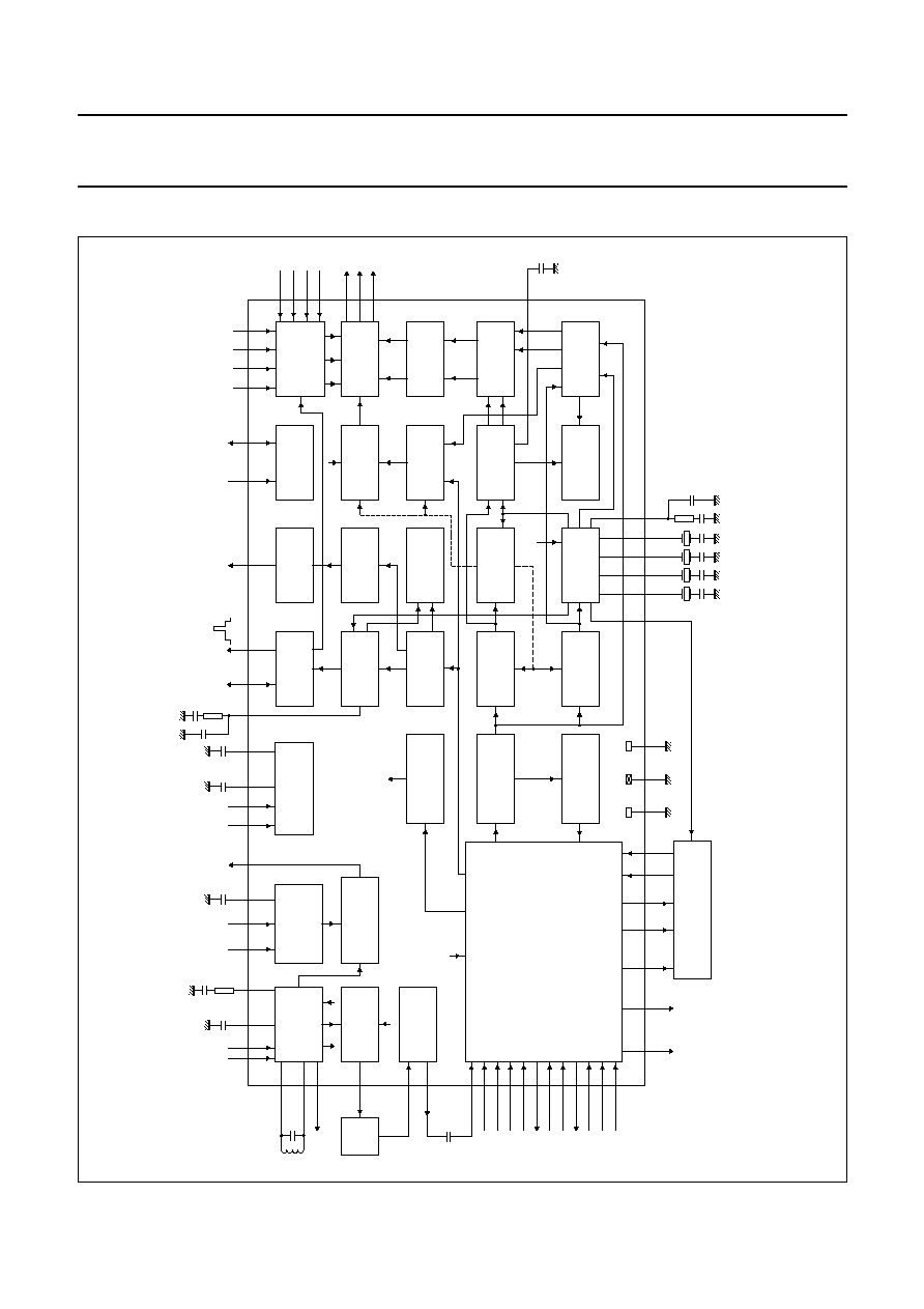
BLOCK DIAGRAM
MGR473
a
ndbook, full pagewidth
3
2
8
7
10
12
13
62
VIFVCO2
VIFVCO1
TAGC
AFC
TOP
mute
Y/CVBS
helper
hue
fsc
switch control
VIF AMPLIFIER
AND PLL
DEMODULATOR
AGC/AFC
VIDEO AMPLIFIER
MUTE
SUPPLY
PULSE
GENERATOR
SOUND
TRAP
GROUP DELAY
CORRECTION
VIDEO SWITCHES
AND
CONTROL
VIFO
GDI
GDO
48
AS
24
C4
23
CVBS/Y4
22
SW1
21
C3
20
CVBS/Y3
19
SW0
18
CVBS2
17
AV2
16
CVBS1
15
AV1
14
CVBSint
6
4
VIF1
VIF2 DECVIF
VCO AND
HORIZONTAL
PLL
VIDEO
IDENTIFICATION
IDENT
SYNC
SEPARATOR
AUTOMATIC
CHROMINANCE
CONTROL
CLOCHE
FILTER
VERTICAL
DIVIDER
SYNC
IN-LOCK
DETECTOR
FILTER
TUNING
I
2
C-BUS
TRANSCEIVER
Y-DELAY
Y-delay
RGB2
VO
Y-SWITCH
AND TRAPS
SECAM
DECODER
RGB MATRIX
Y/U/V
SWITCH
BASEBAND
DELAY LINE
PAL(NTSC)/
SECAM SWITCH
Y/C
DETECTOR
BANDPASS
FILTER
subcarrier
COMB FILTER
PAL/NTSC
PLL
HUE CONTROL
SYSTEM
IDENTIFICATION
PAL/NTSC
DEMODULATOR
63
SIF AMPLIFIER
AGC
QSS MIXER
AM DEMODULATOR
1
SIF1
60
HA/CLP
59
SCO
61
VA
46
SCL
47
SDA
36
37
GI1
RI1
38
BI1
39
RGB1
64
SIF2
DECSIF
11
33
VP1
5
QSS/AM
45
VP2 DECDIG
35
DECBG
VIFPLL
VERTICAL
SYNC
SEPARATOR
58
40
BI2
43
GI2
42
RI2
41
53
51
UO
V
U
V
U
B-Y
R-Y
Y
Y
Y
50
YO
49
DECSEC
PH1LF
57
56
55
54
30
REFO
29
CCF
28
YCF
27
SYS2
25
SYS1
26
CVBSCF
32
CVBSPIP
34
CVBSTXT
52
LFBP
XTALD
XTALC
XTALB
XTALA
44
GND3
31
GND2
9
GND1
TDA9321H
Fig.1 Block diagram.

1998 Dec 16
5
Philips Semiconductors
Preliminary specification
I
2
C-bus controlled TV input processor
TDA9321H
PINNING
SYMBOL
PIN
DESCRIPTION
DEC
SIF
1
SIF AGC decoupling
VIF1
2
VIF input 1
VIF2
3
VIF input 2
DEC
VIF
4
VIF AGC decoupling
QSS/AM
5
combined QSS and AM sound output
VIFPLL
6
VIF PLL filter
VIFVCO1
7
VIF VCO tuned circuit 1
VIFVCO2
8
VIF VCO tuned circuit 2
GND1
9
main supply ground
VIFO
10
VIF output
V
P1
11
positive supply 1 (+8 V)
GDI
12
group delay correction input
GDO
13
group delay correction output
CVBS
int
14
internal CVBS input
AV1
15
AV input 1
CVBS1
16
CVBS input 1
AV2
17
AV input 2
CVBS2
18
CVBS input 2
SW0
19
switch output bit 0 (I
2
C-bus)
CVBS/Y3
20
CVBS or luminance input 3
C3
21
chrominance input 3
SW1
22
switch output bit 1 (I
2
C-bus)
CVBS/Y4
23
CVBS or luminance input 4
C4
24
chrominance input 4
SYS1
25
system output 1 for comb filter
CVBSCF
26
CVBS output for comb filter
SYS2
27
system output 2 for comb filter
YCF
28
luminance input from comb filter
CCF
29
chrominance input from comb filter
REFO
30
reference output (subcarrier)
GND2
31
digital supply ground
CVBSPIP
32
CVBS output for Picture-In-Picture
DEC
DIG
33
digital supply decoupling
CVBSTXT
34
CVBS output for teletext
DEC
BG
35
band gap decoupling
RI1
36
red input 1
GI1
37
green input 1
BI1
38
blue input 1
RGB1
39
RGB insertion input 1
RGB2
40
RGB insertion input 2
RI2
41
red input 2
GI2
42
green input 2
BI2
43
blue input 2
GND3
44
ground 3
V
P2
45
positive supply 2 (+8 V)
SCL
46
serial clock input (I
2
C-bus)
SDA
47
serial data input/output (I
2
C-bus)
AS
48
address select input (I
2
C-bus)
YO
49
luminance output
UO
50
U-signal output
VO
51
V-signal output
LFBP
52
loop filter burst phase detector
DEC
SEC
53
SECAM PLL decoupling
XTALA
54
crystal A (4.433619 MHz)
XTALB
55
crystal B (3.582056 MHz)
XTALC
56
crystal C (3.575611 MHz)
XTALD
57
crystal D (3.579545 MHz)
PH1LF
58
phase 1 loop filter
SCO
59
sandcastle pulse output
HA/CLP
60
horizontal pulse output or clamp pulse
input/output
VA
61
vertical pulse output
TAGC
62
tuner AGC output
SIF1
63
SIF input 1
SIF2
64
SIF input 2
SYMBOL
PIN
DESCRIPTION
