2000 May 08
2
Philips Semiconductors
Preliminary specification
I
2
C-bus controlled TV display processors
TDA933xH series
FEATURES
Available in all ICs:
∑
Can be used in both single scan (50 or 60 Hz) and
double scan (100 or 120 Hz) applications
∑
YUV input and linear RGB input with fast blanking
∑
Separate OSD/text input with fast blanking or blending
∑
Black stretching of non-standard luminance signals
∑
Switchable matrix for the colour difference signals
∑
RGB control circuit with Continuous Cathode Calibration
(CCC), plus white point and black level offset
adjustment
∑
Blue stretch circuit which offsets colours near white
towards blue
∑
Internal clock generation for the deflection processing,
which is synchronized by a 12 MHz ceramic resonator
oscillator
∑
Horizontal synchronization with two control loops and
alignment-free horizontal oscillator
∑
Slow start and slow stop of the horizontal drive pulses
∑
Low-power start-up option for the horizontal drive circuit
∑
Vertical count-down circuit
∑
Vertical driver optimized for DC-coupled vertical output
stages
∑
Vertical and horizontal geometry processing
∑
Horizontal and vertical zoom possibility and vertical
scroll function for application with 16 : 9 picture tubes
∑
Horizontal parallelogram and bow correction
∑
I
2
C-bus control of various functions
∑
Low dissipation.
GENERAL DESCRIPTION
The TDA933xH series are display processors for
`High-end' television receivers which contain the following
functions:
∑
RGB control processor with Y, U and V inputs, a linear
RGB input for SCART or VGA signals with fast blanking,
a linear RGB input for OSD and text signals with a fast
blanking or blending option and an RGB output stage
with black current stabilization, which is realized with the
CCC (2-point black current measurement) system.
∑
Programmable deflection processor with internal clock
generation, which generates the drive signals for the
horizontal, East-West (E-W) and vertical deflection.
The circuit has various features that are attractive for the
application of 16 : 9 picture tubes.
∑
The circuit can be used in both single scan (50 or 60 Hz)
and double scan (100 or 120 Hz) applications.
In addition to these functions, the TDA9331H and
TDA9332H have a multi-sync function for the horizontal
PLL, with a frequency range from 30 to 50 kHz (2f
H
mode)
or 15 to 25 kHz (1f
H
mode), so that the ICs can also be
used to display SVGA signals.
The supply voltage of the ICs is 8 V. They are each
contained in a 44-pin QFP package.
ORDERING INFORMATION
TYPE
NUMBER
PACKAGE
NAME
DESCRIPTION
VERSION
TDA9330H
QFP44
plastic quad flat package; 44 leads (lead length 1.3 mm);
body 10
◊
10
◊
1.75 mm
SOT307-2
TDA9331H
TDA9332H
2000 May 08
3
Philips Semiconductors
Preliminary specification
I
2
C-bus controlled TV display processors
TDA933xH series
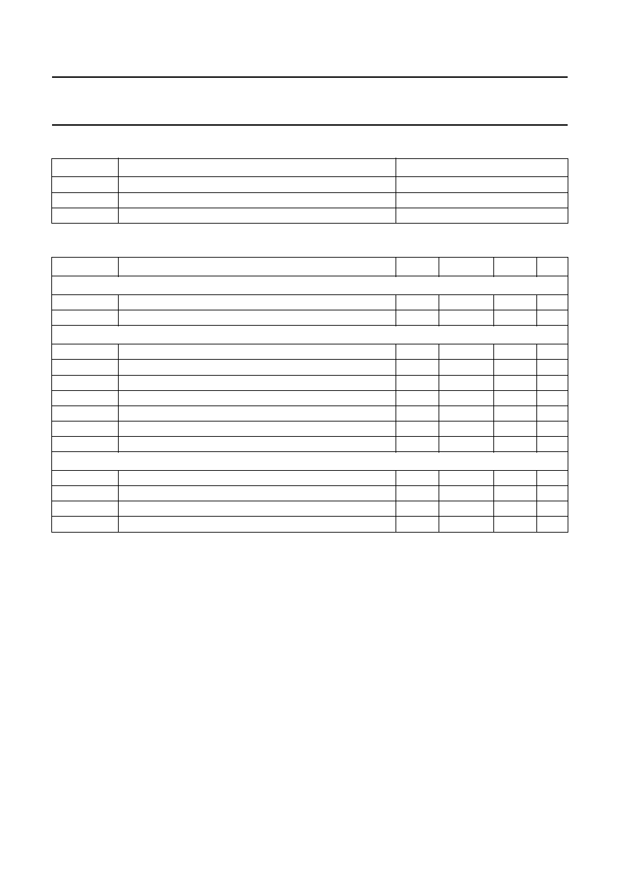
SURVEY OF IC TYPES
QUICK REFERENCE DATA
IC VERSION
VGA MODE
DAC OUTPUT
TDA9330H
no
I
2
C-bus controlled
TDA9331H
yes
proportional to VGA frequency
TDA9332H
yes
I
2
C-bus controlled
SYMBOL
PARAMETER
MIN.
TYP.
MAX.
UNIT
Supply
V
P
supply voltage
-
8.0
-
V
I
P
supply current (V
P1
plus V
P2
)
-
50
-
mA
Input voltages
V
i(Y)(b-w)
luminance input signal (black-to-white value)
-
1.0/0.315
-
V
V
i(U)(p-p)
U input signal (peak-to-peak value)
-
1.33
-
V
V
i(V)(p-p)
V input signal (peak-to-peak value)
-
1.05
-
V
V
i(RGB)(b-w)
RGB input signal (black-to-white value)
-
0.7
-
V
V
i(Hsync)
horizontal sync input (H
D
)
-
TTL
-
V
V
i(Vsync)
vertical sync input (V
D
)
-
TTL
-
V
V
i(IIC)
I
2
C-bus inputs (SDA and SCL)
-
CMOS 5 V
-
V
Output signals
V
o(RGB)(b-w)
RGB output signal amplitude (black-to-white value)
-
2.0
-
V
I
o(hor)
horizontal output current
-
-
10
mA
I
o(ver)(p-p)
vertical output current (peak-to-peak value)
-
0.95
-
mA
I
o(EW)
E-W drive output current
-
-
1.2
mA

2000 May 08
5
Philips Semiconductors
Preliminary specification
I
2
C-bus controlled TV display processors
TDA933xH series
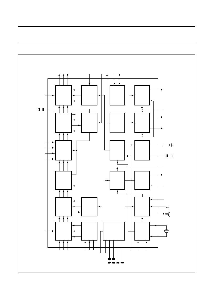
PINNING
SYMBOL
PIN
DESCRIPTION
VDOA
1
vertical drive output A
VDOB
2
vertical drive output B
EWO
3
E-W output
EHTIN
4
EHT compensation input
FLASH
5
flash detection input
GND1
6
ground 1
DEC
VD
7
digital supply decoupling
HOUT
8
horizontal output
SCO
9
sandcastle pulse output
SCL
10
serial clock input
SDA
11
serial data input/output
HSEL
12
selection of horizontal frequency
HFB
13
horizontal flyback pulse input
DPC
14
dynamic phase compensation
VSC
15
vertical sawtooth capacitor
I
ref
16
reference current input
V
P1
17
positive supply 1 (+8 V)
DEC
BG
18
band gap decoupling
GND2
19
ground 2
XTALI
20
crystal input
XTALO
21
crystal output
LPSU
22
low-power start-up supply
V
D
23
vertical sync input
H
D
24
horizontal sync input
DACOUT
25
DAC output
VIN
26
V-signal input
UIN
27
U-signal input
YIN
28
luminance input
FBCSO
29
fixed beam current switch-off input
RI1
30
red 1 input for insertion
GI1
31
green 1 input for insertion
BI1
32
blue 1 input for insertion
BL1
33
fast blanking input for RGB-1
PWL
34
peak white limiting decoupling
RI2
35
red 2 input for insertion
GI2
36
green 2 input for insertion
BI2
37
blue 2 input for insertion
BL2
38
fast blanking/blending input for RGB-2
V
P2
39
positive supply 2 (+8 V)
RO
40
red output