Document Outline
- FEATURES
- GENERAL DESCRIPTION
- ORDERING INFORMATION
- SURVEY OF IC TYPES
- QUICK REFERENCE DATA
- BLOCK DIAGRAM
- PINNING
- FUNCTIONAL DESCRIPTION
- I 2 C-BUS SPECIFICATION
- LIMITING VALUES
- THERMAL CHARACTERISTICS
- QUALITY SPECIFICATION
- CHARACTERISTICS
- TEST AND APPLICATION INFORMATION
- PACKAGE OUTLINE
- SOLDERING
- DATA SHEET STATUS
- DEFINITIONS
- DISCLAIMERS
- PURCHASE OF PHILIPS I 2 C COMPONENTS

DATA SHEET
Preliminary specification
Supersedes data of 2000 May 08
2002 Jun 04
INTEGRATED CIRCUITS
TDA933xH series
I
2
C-bus controlled TV display
processors

2002 Jun 04
2
Philips Semiconductors
Preliminary specification
I
2
C-bus controlled TV display processors
TDA933xH series
FEATURES
Available in all ICs:
∑
Can be used in both single scan (50 or 60 Hz) and
double scan (100 or 120 Hz) applications
∑
YUV input and linear RGB input with fast blanking
∑
Separate OSD/text input with fast blanking or blending
∑
Black stretching of non-standard luminance signals
∑
Switchable matrix for the colour difference signals
∑
RGB control circuit with Continuous Cathode Calibration
(CCC), plus white point and black level offset
adjustment
∑
Blue stretch circuit which offsets colours near white
towards blue
∑
Internal clock generation for the deflection processing,
which is synchronized by a 12 MHz ceramic resonator
oscillator
∑
Horizontal synchronization with two control loops and
alignment-free horizontal oscillator
∑
Slow start and slow stop of the horizontal drive pulses
∑
Low-power start-up option for the horizontal drive circuit
∑
Vertical count-down circuit
∑
Vertical driver optimized for DC-coupled vertical output
stages
∑
Vertical and horizontal geometry processing
∑
Horizontal and vertical zoom possibility and vertical
scroll function for application with 16 : 9 picture tubes
∑
Horizontal parallelogram and bow correction
∑
I
2
C-bus control of various functions
∑
Low dissipation.
GENERAL DESCRIPTION
The TDA933xH series are display processors for
`High-end' television receivers which contain the following
functions:
∑
RGB control processor with Y, U and V inputs, a linear
RGB input for SCART or VGA signals with fast blanking,
a linear RGB input for OSD and text signals with a fast
blanking or blending option and an RGB output stage
with black current stabilization, which is realized with the
CCC (2-point black current measurement) system.
∑
Programmable deflection processor with internal clock
generation, which generates the drive signals for the
horizontal, East-West (E-W) and vertical deflection.
The circuit has various features that are attractive for the
application of 16 : 9 picture tubes.
∑
The circuit can be used in both single scan (50 or 60 Hz)
and double scan (100 or 120 Hz) applications.
In addition to these functions, the TDA9331H and
TDA9332H have a multi-sync function for the horizontal
PLL, with a frequency range from 30 to 50 kHz (2f
H
mode)
or 15 to 25 kHz (1f
H
mode), so that the ICs can also be
used to display SVGA signals.
The supply voltage of the ICs is 8 V. They are each
contained in a 44-pin QFP package.
ORDERING INFORMATION
TYPE
NUMBER
PACKAGE
NAME
DESCRIPTION
VERSION
TDA9330H
QFP44
plastic quad flat package; 44 leads (lead length 1.3 mm);
body 10
◊
10
◊
1.75 mm
SOT307-2
TDA9331H
TDA9332H
2002 Jun 04
3
Philips Semiconductors
Preliminary specification
I
2
C-bus controlled TV display processors
TDA933xH series
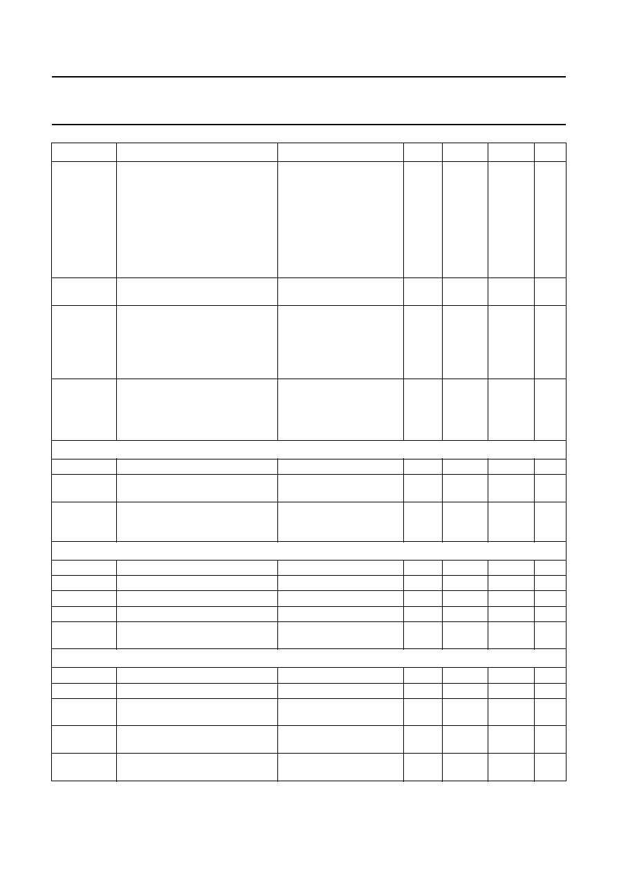
SURVEY OF IC TYPES
QUICK REFERENCE DATA
IC VERSION
VGA MODE
DAC OUTPUT
TDA9330H
no
I
2
C-bus controlled
TDA9331H
yes
proportional to VGA frequency
TDA9332H
yes
I
2
C-bus controlled
SYMBOL
PARAMETER
MIN.
TYP.
MAX.
UNIT
Supply
V
P
supply voltage
-
8.0
-
V
I
P
supply current (V
P1
plus V
P2
)
-
50
-
mA
Input voltages
V
i(Y)(b-w)
luminance input signal (black-to-white value)
-
1.0/0.315
-
V
V
i(U)(p-p)
U input signal (peak-to-peak value)
-
1.33
-
V
V
i(V)(p-p)
V input signal (peak-to-peak value)
-
1.05
-
V
V
i(RGB)(b-w)
RGB input signal (black-to-white value)
-
0.7
-
V
V
i(Hsync)
horizontal sync input (H
D
)
-
TTL
-
V
V
i(Vsync)
vertical sync input (V
D
)
-
TTL
-
V
V
i(IIC)
I
2
C-bus inputs (SDA and SCL)
-
CMOS 5 V
-
V
Output signals
V
o(RGB)(b-w)
RGB output signal amplitude (black-to-white value)
-
2.0
-
V
I
o(hor)
horizontal output current
-
-
10
mA
I
o(ver)(p-p)
vertical output current (peak-to-peak value)
-
0.95
-
mA
I
o(EW)
E-W drive output current
-
-
1.2
mA

2002
Jun
04
4
Philips Semiconductors
Preliminar
y specification
I
2
C-b
us controlled TV displa
y processors
TD
A933xH ser
ies
2002
Jun
04
4
Philips Semiconductors
Preliminar
y specification
I
2
C-b
us controlled TV displa
y processors
TD
A933xH ser
ies
This text is here in white to force landscape pages to be rotated correctly when browsing through the pdf in the Acrobat reader.This text is here in
_
white to force landscape pages to be rotated correctly when browsing through the pdf in the Acrobat reader.This text is here inThis text is here in
white to force landscape pages to be rotated correctly when browsing through the pdf in the Acrobat reader. white to force landscape pages to be ...
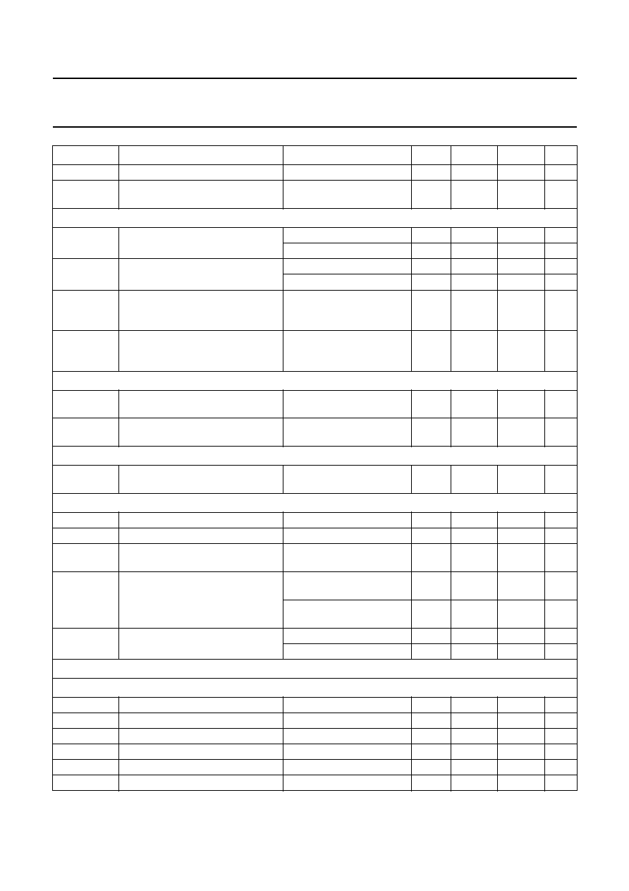
BLOCK DIA
GRAM
handbook, full pagewidth
MGR445
SWITCH
Y
Y
U
V
SAT
CONTR
U
V
SATURATION
CONTROL
COLOUR
DIFFERENCE
MATRIX
R
G
B
CONTRAST
CONTROL
R
G
B
RGB
INSERTION
R
G
G
B
BRI
white
point
WHITE POINT
AND
BRIGHTNESS
CONTROL
R
B
OUTPUT
AMPLIFIER
AND
BUFFER
BLUE STRETCH
40
41
42
28
27
26
YIN
UIN
VIN
RGB-YUV
MATRIX
BLACK
STRETCH
PWL
AND
BEAM
CURRENT
LIMITER
CONTINUOUS
CATHODE
CALIBRATION
44
30
31
32
RI1
GI1
BI1
SUPPLY
H-SHIFT
SOFT
START/STOP
LOW-POWER
START-UP
H/V DIVIDER
19
◊
6-BIT DACs
2
◊
4-BIT DACs
I
2
C-BUS
TRANSCEIVER
10
43
11
25
18
6
19
17
7
39
DECBG
GND1
GND2
23
VP1
DECVD
VP2
CLOCK
GENERATION
AND
1st LOOP
20
21
13
14
22
PHASE-2
LOOP
HORIZONTAL
OUTPUT
15
16
VSC
Iref
RAMP
GENERATOR
1
2
4
VERTICAL
GEOMETRY
3
E-W
GEOMETRY
GEOMETRY CONTROL
24
12
HSEL
33
29
38
37
36
35
34
TDA933xH
BL1
FBCSO
BL2
GI2
RI2
PWL
BI2
BCL
BO
GO
RO
BLKIN
DACOUT
SDA
SCL
VDOA
5
8
9
VDOB
EWO
EHTIN
XTALI
XTALO
LPSU
FLASH
HOUT
SCO
HFB
DPC
HD
VD
Fig.1 Block diagram.

2002 Jun 04
5
Philips Semiconductors
Preliminary specification
I
2
C-bus controlled TV display processors
TDA933xH series
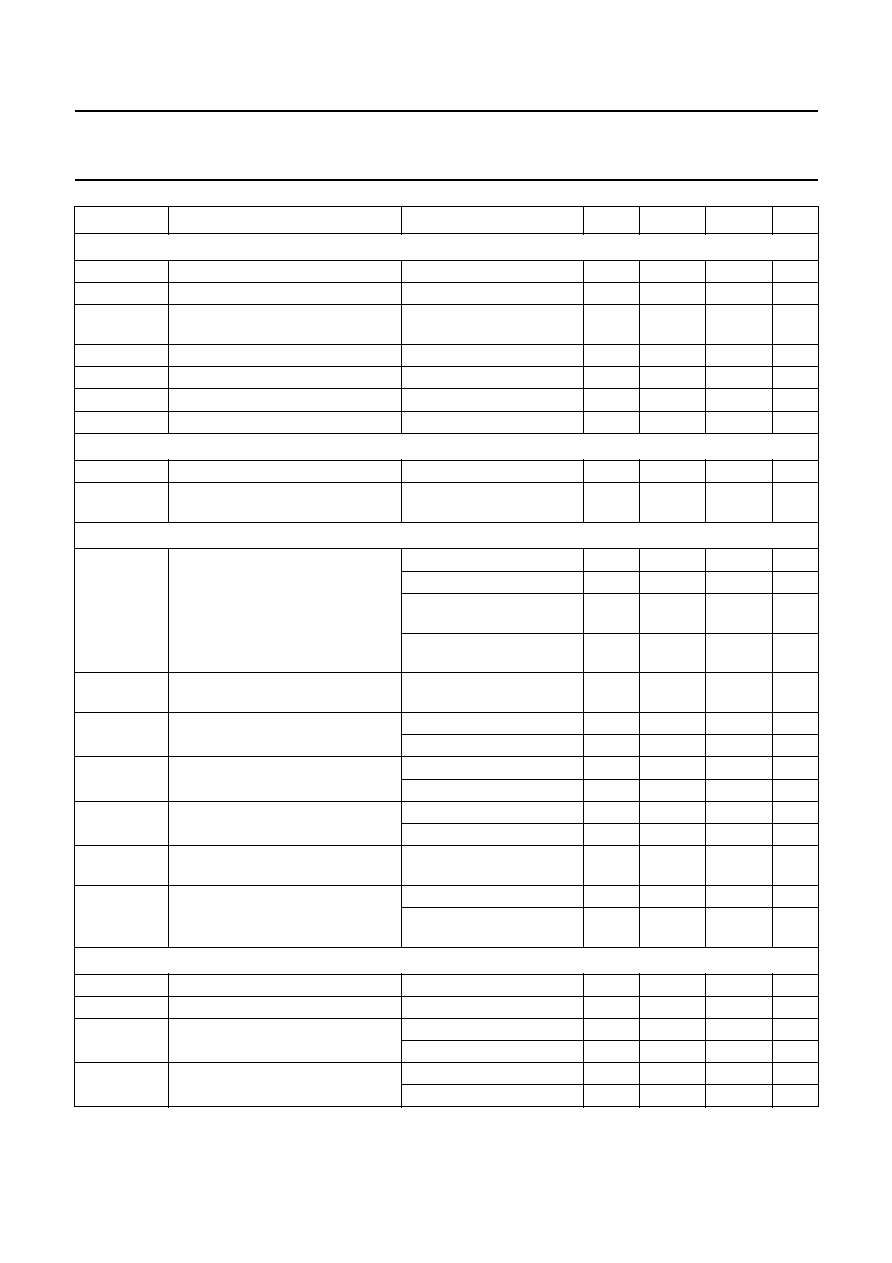
PINNING
SYMBOL
PIN
DESCRIPTION
VDOA
1
vertical drive output A
VDOB
2
vertical drive output B
EWO
3
E-W output
EHTIN
4
EHT compensation input
FLASH
5
flash detection input
GND1
6
ground 1
DEC
VD
7
digital supply decoupling
HOUT
8
horizontal output
SCO
9
sandcastle pulse output
SCL
10
serial clock input
SDA
11
serial data input/output
HSEL
12
selection of horizontal frequency
HFB
13
horizontal flyback pulse input
DPC
14
dynamic phase compensation
VSC
15
vertical sawtooth capacitor
I
ref
16
reference current input
V
P1
17
positive supply 1 (+8 V)
DEC
BG
18
band gap decoupling
GND2
19
ground 2
XTALI
20
crystal input
XTALO
21
crystal output
LPSU
22
low-power start-up supply
V
D
23
vertical sync input
H
D
24
horizontal sync input
DACOUT
25
DAC output
VIN
26
V-signal input
UIN
27
U-signal input
YIN
28
luminance input
FBCSO
29
fixed beam current switch-off input
RI1
30
red 1 input for insertion
GI1
31
green 1 input for insertion
BI1
32
blue 1 input for insertion
BL1
33
fast blanking input for RGB-1
PWL
34
peak white limiting decoupling
RI2
35
red 2 input for insertion
GI2
36
green 2 input for insertion
BI2
37
blue 2 input for insertion
BL2
38
fast blanking/blending input for RGB-2
V
P2
39
positive supply 2 (+8 V)
RO
40
red output
2002 Jun 04
6
Philips Semiconductors
Preliminary specification
I
2
C-bus controlled TV display processors
TDA933xH series
GO
41
green output
BO
42
blue output
BCL
43
beam current limiting input
BLKIN
44
black current input
SYMBOL
PIN
DESCRIPTION
handbook, full pagewidth
1
2
3
4
5
6
7
8
9
10
11
33
32
31
30
29
28
27
26
25
24
23
12
13
14
15
16
17
18
19
20
21
22
44
43
42
41
40
39
38
37
36
35
34
TDA933xH
MGR446
BL1
BI1
GI1
RI1
YIN
UIN
VIN
DACOUT
HD
VD
VDOA
VDOB
EWO
EHTIN
FLASH
GND1
HOUT
SCO
SDA
FBCSO
BCL
BO
GO
RO
V
P2
BL2
GI2
RI2
PWL
BLKIN
BI2
HFB
DPC
VSC
I ref
V
P1
DEC
BG
XTALI
XTALO
LPSU
HSEL
GND2
DECVD
SCL
Fig.2 Pin configuration.

2002 Jun 04
7
Philips Semiconductors
Preliminary specification
I
2
C-bus controlled TV display processors
TDA933xH series
FUNCTIONAL DESCRIPTION
RGB control circuit
I
NPUT SIGNALS
The RGB control circuit of the TDA933xH contains three
sets of input signals:
∑
YUV input signals, which are supplied by the input
processor or the feature box. Bit GAI can be used to
switch the luminance input signal sensitivity between
0.45 V (p-p) and 1.0 V (b-w). The nominal input signals
for U and V are 1.33 V (p-p) and 1.05 V (p-p),
respectively. These input signals are controlled on
contrast, saturation and brightness.
∑
The first RGB input is intended for external signals
(SCART in 1f
H
and VGA in 2f
H
applications), which have
an amplitude of 0.7 V (p-p) typical. This input is also
controlled on contrast, saturation and brightness.
∑
The second RGB input is intended for OSD and teletext
signals. The required input signals have an amplitude of
0.7 V (p-p). The switching between the internal signal
and the OSD signal can be realized via a blending
function or via fast blanking. This input is only controlled
on brightness.
Switching between the various sources can be realized via
the I
2
C-bus and by fast insertion switches. The fast
insertion switches can be enabled via the I
2
C-bus.
The circuit contains switchable matrix circuits for the
colour difference signals so that the colour reproduction
can be adapted for PAL/SECAM and NTSC. For NTSC,
two different matrices can be chosen. In addition, a matrix
for high-definition ATSC signals is available.
O
UTPUT AMPLIFIER
The output signal has an amplitude of approximately
2 V (b-w) at nominal input signals and nominal settings of
the controls. The required `white point setting' of the
picture tube can be realized by means of three separate
gain settings for the RGB channels.
To obtain an accurate biasing of the picture tube, a CCC
circuit has been developed. This function is realized by a
2-point black level stabilization circuit.
By inserting two test levels for each gun and comparing the
resulting cathode currents with two different reference
currents, the influence of the picture tube parameters such
as the spread in cut-off voltage can be eliminated.
This 2-point stabilization is based on the principle that the
ratio between the cathode currents is coupled to the ratio
between the drive voltages according to:
The feedback loop makes the ratio between cathode
currents I
k1
and I
k2
equal to the ratio between the
reference currents (which are internally fixed) by changing
the (black) level and the amplitude of the RGB output
signals via two converging loops. The system operates in
such a way that the black level of the drive signal is
controlled to the cut-off point of the gun. In this way, a very
good grey scale tracking is obtained. The accuracy of the
adjustment of the black level is only dependent on the ratio
of internal currents and these can be made very accurately
in integrated circuits. An additional advantage of the
2-point measurement is that the control system makes the
absolute value of I
k1
and I
k2
identical to the internal
reference currents. Because this adjustment is obtained
by adapting the gain of the RGB control stage, this control
stabilizes the gain of the complete channel (RGB output
stage and cathode characteristic). As a result, this 2-point
loop compensates for variations in the gain figures during
life.
An important property of the 2-point stabilization is that the
offset and the gain of the RGB path are adjusted by the
feedback loop. Hence, the maximum drive voltage for the
cathode is fixed by the relationship between the test
pulses, the reference current and the relative gain setting
of the three channels. Consequently, the drive level of the
CRT cannot be adjusted by adapting the gain of the RGB
output stage. Because different picture tubes may require
different drive levels, the typical `cathode drive level'
amplitude can be adjusted by means of an I
2
C-bus setting.
Depending on the selected cathode drive level, the typical
gain of the RGB output stages can be fixed, taking into
account the drive capability of the RGB outputs
(pins 40 to 42). More details about the design are given in
the application report (see also Chapter "Characteristics";
note 11).
The measurement of the high and the low currents of the
2-point stabilization circuit is performed in two consecutive
fields. The leakage current is measured in each field. The
maximum allowable leakage current is 100
µ
A.
For extra flexibility, it also possible to switch the CCC
circuit to 1-point stabilization with the OPC bit. In this
mode, only the black level at the RGB outputs is controlled
by the loop. The cathode drive level setting has no
influence on the gain in this mode. This level should be set
to the nominal value to get the correct amplitude of the
measuring pulses.
I
k1
I
k2
-------
V
dr1
V
dr1
-----------
=

2002 Jun 04
8
Philips Semiconductors
Preliminary specification
I
2
C-bus controlled TV display processors
TDA933xH series
Via the I
2
C-bus, an adjustable offset can be made on the
black level of red and green channels with respect to the
level that is generated by the black current control loop.
These controls can be used to adjust the colour
temperature of the dark part of the picture, independent of
the white point adjustment.
When the TV receiver is switched on, the black current
stabilization circuit is directly activated and the RGB
outputs are blanked. The blanking is switched off as soon
as the loop has stabilized (e.g. the first time that bit BCF
changes from 1 to 0, see also Chapter "Characteristics";
note 15). This ensures that the switch-on time is reduced
to a minimum and is only dependent on the warm-up time
of the picture tube.
The black current stabilization system checks the output
level of the three channels and indicates whether the black
level of the lowest RGB output of the IC is in a certain
window (WBC bit), below or above this window (HBC bit).
This indication can be read from the I
2
C-bus and can be
used for automatic adjustment of voltage V
g2
during the
production of the TV receiver.
When a failure occurs in the black current loop (e.g. due to
an open circuit), status bit BCF is set. This information can
be used to blank the picture tube to avoid damage to the
screen.
The control circuit contains an average beam current
limiting circuit and a peak white level (PWL) circuit. The
PWL detects small white areas in the picture that are not
detected by the average beam current limiter. The PWL
can be adjusted via the I
2
C-bus. A low-pass filter is placed
in front of the peak detector to prevent it from reacting to
short transients in the video signal. The capacitor of the
low-pass filter is connected externally so that the set
maker can adapt the time constant as required. The IC
also contains a soft clipper that limits the amplitude of the
short transients in the RGB output signals. In this way, spot
blooming on, for instance, subtitles is prevented. The
difference between the PWL and the soft clipping level can
be adjusted via the I
2
C-bus in a few steps.
The vertical blanking is adapted to the vertical frequency
of the incoming signal (50 or 100 Hz or, 60 or 120 Hz).
When the flyback time of the vertical output stage is
greater than the 60 Hz blanking time, the blanking can be
increased to the same value as that of the 50 Hz blanking.
This can be set by means of bit LBM.
When no video is available, it is possible to insert a blue
background. This feature can be activated via bit EBB.
Synchronization and deflection processing
H
ORIZONTAL SYNCHRONIZATION AND DRIVE CIRCUIT
The horizontal drive signal is obtained from an internal
VCO which runs at a frequency of 440 times (2f
H
mode) or
880 times (1f
H
mode) the frequency of the incoming H
D
signal. The free-running frequency of this VCO is
calibrated by a crystal oscillator which needs an external
12 MHz crystal or ceramic resonator as a reference. It is
also possible to supply an external reference signal to the
IC (in this case, the external resonator should be
removed).
The VCO is synchronized to the incoming horizontal H
D
pulse (applied from the feature box or the input processor)
by a PLL with an internal time constant. The frequency of
the horizontal drive signal (1f
H
or 2f
H
) is selected by means
of a switching pin, which must be connected to ground or
left open-circuit.
For HDTV applications, it is possible to change the
free-running frequency of the horizontal drive output. For
the 1080i-60 Hz scanning system the free-running
frequency can be increased to 33.8 kHz with the HDTV bit,
while for the 1080i-50 Hz system (China and Australia) the
free-running frequency can be decreased to 28.5 kHz with
the CDTV bit.
For safety reasons, switching between 1f
H
and 2f
H
modes is only possible when the IC is in the standby
mode.
For the TDA9331H and TDA9332H, it is also possible to
set the horizontal PLL to a `multi-sync' mode by means of
bit VGA. In this mode, the circuit detects the frequency of
the incoming sync pulses and adjusts the centre frequency
of the VCO accordingly by means of an internal
Digital-to-Analog-Converter (DAC). The frequency range
in this mode is 30 to 50 kHz at the output.
The polarities of the incoming H
D
and V
D
pulses are
detected internally. The detected polarity can be read out
via status bits HPOL and VPOL.
The horizontal drive signal is generated by a second
control loop which compares the phase of the reference
signal (applied from the internal VCO) with the flyback
pulse. The time constant of this loop is set internally. The
IC has a dynamic horizontal phase correction input, which
can be used to compensate phase shifts that are caused
by beam current variations. Additional settings of the
horizontal deflection (which are realized via the second
loop) are the horizontal shift and horizontal parallelogram
and bow corrections (see Chapter "Characteristics";
Fig.16). The adjustments are realized via the I
2
C-bus.

2002 Jun 04
9
Philips Semiconductors
Preliminary specification
I
2
C-bus controlled TV display processors
TDA933xH series
When no horizontal flyback pulse is detected during three
consecutive line periods, status bit NHF is set (output
status byte 01-D3; see Table 3).
The horizontal drive signal is switched on and off via the
so-called slow-start/slow-stop procedure. This function is
realized by varying the t
on
of the horizontal drive pulse. For
EHT generators without a bleeder, the IC can be set to a
`fixed beam current mode' via bit FBC. In this case, the
picture tube capacitance is discharged with a current of
approximately 1 mA. The magnitude of the discharge
current is controlled via the black current feedback loop.
If necessary, the discharge current can be enlarged with
the aid of an external current division circuit. With the fixed
beam current option activated, it is still possible to have a
black screen during switch-off. This can be realized by
placing the vertical deflection in an overscan position. This
mode is activated via bit OSO.
An additional mode of the IC is the `low-power start-up'
mode. This mode is activated when a supply voltage of 5 V
is supplied to the start-up pin.
The required current for this mode is 3 mA (typ.). In this
condition, the horizontal drive signal has the nominal t
off
and the t
on
grows gradually from zero to approximately
30% of the nominal value. This results in a line frequency
of approximately 50 kHz (2f
H
) or 25 kHz (1f
H
). The output
signal remains unchanged until the main supply voltage is
switched on and the I
2
C-bus data has been received. The
horizontal drive then gradually changes to the nominal
frequency and duty cycle via the slow-start procedure.
The IC can only be switched on and to standby mode when
both standby bits (STB0 and STB1) are changed. The
circuit will not react when only one bit changes polarity.
The IC has a general purpose bus controlled DAC output
with a 6-bit resolution and with an output voltage range
between 0.2 to 4 V. In the TDA9331H, the DC voltage on
this output is proportional to the horizontal line frequency
(only in VGA mode). This voltage can be used to control
the supply voltage of the horizontal deflection stage, to
maintain constant picture width for higher line frequencies.
V
ERTICAL DEFLECTION AND GEOMETRY CONTROL
The drive signals for the vertical and E-W deflection
circuits are generated by a vertical divider, which derives
its clock signal from the line oscillator. The divider is
synchronized by the incoming V
D
pulse, generated by the
input processor or the feature box. The vertical ramp
generator requires an external resistor and capacitor; the
tolerances for these components must be small.
In the normal mode, the vertical deflection operates in
constant slope and adapts its amplitude, depending on the
frequency of the incoming signal (50 or 60 Hz, or
100 or 120 Hz). When the TDA933xH is switched to the
VGA mode, the amplitude of the vertical scan is stabilized
and independent of the incoming vertical frequency. In this
mode, the E-W drive amplitude is proportional to the
horizontal frequency so that the correction on the screen is
not affected.
The vertical drive is realized by a differential output
current. The outputs must be DC-coupled to the vertical
output stage (e.g. TDA8354).
The vertical geometry can be adjusted via the I
2
C-bus.
Controls are possible for the following parameters:
∑
Vertical amplitude
∑
S-correction
∑
Vertical slope
∑
Vertical shift (only for compensation of offsets in output
stage or picture tube)
∑
Vertical zoom
∑
Vertical scroll (shifting the picture in the vertical direction
when the vertical scan is expanded)
∑
Vertical wait, an adjustable delay for the start of the
vertical scan.
With regard to the vertical wait, the following conditions are
valid:
∑
In the 1f
H
TV mode, the start of the vertical scan is fixed
and cannot be adjusted with the vertical wait
∑
In the 2f
H
TV mode, the start of the vertical scan
depends on the value of the Vertical Scan Reference
(VSR) bus bit. If VSR = 0, the start of the vertical scan is
related to the end of the incoming V
D
pulse. If VSR = 1,
it is related to the start. In both cases, the start of the
scan can be adjusted with the vertical wait setting
∑
In the multi-sync mode (TDA9331H and TDA9332H
both in 1f
H
mode and 2f
H
mode), the start of the vertical
scan is related to the start of the incoming V
D
pulse and
can be adjusted with the vertical wait setting.

2002 Jun 04
10
Philips Semiconductors
Preliminary specification
I
2
C-bus controlled TV display processors
TDA933xH series
The minimum value for the vertical wait setting is 8 line
periods. If the setting is lower than 8, the wait period will
remain at 8 line periods.
The E-W drive circuit has a single-ended output. The E-W
geometry can be adjusted on the following parameters:
∑
Horizontal width with increased range because of the
`zoom' feature
∑
E-W parabola/width ratio
∑
E-W upper corner/parabola ratio
∑
E-W lower corner/parabola ratio
∑
E-W trapezium.
The IC has an EHT compensation input which controls
both the vertical and the E-W output signals. The relative
control effect on both outputs can be adjusted via the
I
2
C-bus (sensitivity of vertical correction is fixed; E-W
correction variable).
To avoid damage to the picture tube in the event of missing
or malfunctioning vertical deflection, a vertical guard
function is available at the sandcastle pin (pin SCO). The
vertical guard pulse from the vertical output stage
(TDA835x) should be connected to the sandcastle pin,
which acts as a current sense input. If the guard pulse is
missing or lasts too long, bit NDF is set in the status
register and the RGB outputs are blanked.
If the guard function is disabled via bit EVG, only status
bit NDF is set.
The IC also has inputs for flash and overvoltage protection.
More details about these functions are given in Chapter
"Characteristics"; note 43.
I
2
C-BUS SPECIFICATION
The slave address of the IC is given in Table 1. The circuit
operates up to clock frequencies of 400 kHz. Valid
subaddresses: 00 to 1F, subaddress FE is reserved for
test purposes. The auto-increment mode is available for
subaddresses. It should be noted that the status bytes
cannot be addressed separately, they can only be read via
the auto-increment mode.
Table 1
Slave address (8C)
A6
A5
A4
A3
A2
A1
A0
R/W
1
0
0
0
1
1
0
1/0

2002 Jun 04
11
Philips Semiconductors
Preliminary specification
I
2
C-bus controlled TV display processors
TDA933xH series
Table 2
Input control bits
Notes
1. For zero parallelogram and bow correction use register value 7 DEC.
2. See Chapter "Characteristics"; note 47.
3. Bit VGA is not available in the TDA9330H.
FUNCTION
SUBADDRESS
(HEX)
DATA BYTE
D7
D6
D5
D4
D3
D2
D1
D0
RGB processing-1
00
MAT
EBB
SBL
RBL
BLS
BKS
IE1
IE2
RGB processing-2
01
MUS
FBC
OBL
AKB
CL3
CL2
CL1
CL0
Wide horizontal blanking
02
HBL
TFBC
GAI
STB0
HB3
HB2
HB1
HB0
Horizontal deflection
03
HDTV
VSR
FAST
STB1
POC
PRD
VGA
(3)
ESS
Vertical deflection
04
OPC
VFF
LBM
DIP
OSO
SVF
EVG
DL
Brightness
05
0
0
A5
A4
A3
A2
A1
A0
Saturation
06
0
0
A5
A4
A3
A2
A1
A0
Contrast
07
0
0
A5
A4
A3
A2
A1
A0
White point R
08
0
0
A5
A4
A3
A2
A1
A0
White point G
09
0
0
A5
A4
A3
A2
A1
A0
White point B
0A
0
0
A5
A4
A3
A2
A1
A0
Peak white limiting
0B
0
0
SC1
SC0
A3
A2
A1
A0
Horizontal shift
0C
0
0
A5
A4
A3
A2
A1
A0
Horizontal parallelogram
(1)
0D
0
0
0
0
A3
A2
A1
A0
E-W width
0E
0
0
A5
A4
A3
A2
A1
A0
E-W parabola/width
0F
0
0
A5
A4
A3
A2
A1
A0
E-W upper corner/parabola
10
0
0
A5
A4
A3
A2
A1
A0
E-W trapezium
11
0
0
A5
A4
A3
A2
A1
A0
E-W EHT compensation sensitivity
12
0
0
A5
A4
A3
A2
A1
A0
Vertical slope
13
0
0
A5
A4
A3
A2
A1
A0
Vertical amplitude
14
0
0
A5
A4
A3
A2
A1
A0
S-correction
15
0
0
A5
A4
A3
A2
A1
A0
Vertical shift
16
0
0
A5
A4
A3
A2
A1
A0
Vertical zoom
17
0
0
A5
A4
A3
A2
A1
A0
Vertical scroll
18
0
0
A5
A4
A3
A2
A1
A0
Vertical wait
19
0
0
0
A4
A3
A2
A1
A0
DAC output
(2)
1A
0
0
A5
A4
A3
A2
A1
A0
Black level offset R
1B
0
0
0
0
A3
A2
A1
A0
Black level offset G
1C
0
0
0
0
A3
A2
A1
A0
Horizontal timing
1D
CDTV
0
0
HDCL
LBL3
LBL2
LBL1
LBL0
E-W lower corner/parabola
1E
0
0
A5
A4
A3
A2
A1
A0
Horizontal bow
(1)
1F
0
0
0
0
A3
A2
A1
A0

2002 Jun 04
12
Philips Semiconductors
Preliminary specification
I
2
C-bus controlled TV display processors
TDA933xH series
Table 3
Output status bits
FUNCTION
SUBADDRESS
(HEX)
DATA BYTE
D7
D6
D5
D4
D3
D2
D1
D0
Output status bytes
00
POR
FSI
SL
XPR
NDF
IN1
IN2
WBC
01
N2
N3
ID1
ID0
NHF
BCF
FLS
NRF
02
X
X
X
X
X
HPOL
VPOL
HBC
Input control bits
Table 4
Colour difference matrix
Table 5
Enable `blue-back'
Table 6
Service blanking
Table 7
RGB blanking
Table 8
Blue stretch
Table 9
Black stretch
Table 10 Enable fast blanking RGB-1
Table 11 Enable fast blanking RGB-2
Table 12 Fixed beam current switch-off
Table 13 Blending function on OSD; note 1
Note
1. When bit OBL is set to 1, the blending function is
always activated, independent of the setting of bit IE2.
Table 14 Black current stabilization
MAT
MUS
MATRIX POSITION
0
0
PAL
0
1
ATSC
1
0
NTSC Japan
1
1
NTSC USA
EBB
MODE
0
blue-black switched off
1
blue-black switched on
SBL
SERVICE BLANKING MODE
0
off
1
on
RBL
RGB BLANKING
0
not active
1
active
BLS
BLUE STRETCH MODE
0
off
1
on
BKS
BLACK STRETCH MODE
0
off
1
on
IE1
FAST BLANKING
0
not active
1
active
IE2
FAST BLANKING
0
not active
1
active
FBC
MODE
0
switch-off with blanked RGB outputs
1
switch-off with fixed beam current
OBL
MODE
0
OSD via fast blanking
1
OSD via blending function
AKB
OPC
MODE
0
0
2-point control
0
1
1-point control
1
-
not active

2002 Jun 04
13
Philips Semiconductors
Preliminary specification
I
2
C-bus controlled TV display processors
TDA933xH series
Table 15 Cathode drive level (15 steps; 3.6 V/step)
Note
1. The given values are valid for the following conditions:
a) Nominal CVBS input signal.
b) Settings for contrast and white point nominal.
c) Black and blue stretch switched off.
d) Gain of output stage such that no clipping occurs.
e) Beam current limiting not active.
f) Gamma of picture tube is 2.25.
g) The tolerance on these values is approximately
±
3 V.
Table 16 RGB blanking mode
Table 17 Picture tube discharge time
Note
1. See Chapter "Characteristics"; Fig.15
Table 18 Gain of luminance channel
Table 19 Standby
Table 20 Position of wide blanking (14 steps; 1f
H
mode
0.29
µ
s/step; 2f
H
mode 0.145
µ
s/step)
Note
1. See Chapter "Characteristics"; note 13.
Table 21 Horizontal free-running frequency in TV mode
Table 22 Vertical scan reference in 2f
H
TV mode
Table 23 Time constant phase-1 loop
Table 24 Synchronization mode
Table 25 Overvoltage input mode
CL3
CL2
CL1
CL0
SETTING OF CATHODE
DRIVE AMPLITUDE
(1)
0
0
0
0
41 V (b-w)
1
0
0
0
70 V (b-w)
1
1
1
1
95 V (b-w)
HBL
MODE
0
normal blanking (horizontal flyback)
1
wide blanking
TFBC
MODE
0
18.6 ms
1
25 ms
GAI
MODE
0
normal gain [V
28
= 1 V (b-w)]
1
high gain [V
28
= 0.45 V (p-p)]
STB0
STB1
CONDITION
0
0
horizontal drive off
0
1
no action
1
0
no action
1
1
horizontal drive on
HB3
HB2
HB1
HB0
TIMING OF BLANKING
(1)
1f
H
MODE
2f
H
MODE
0
0
0
0
-
2.03
µ
s
-
1.015
µ
s
0
1
1
1
0
µ
s
0
µ
s
1
1
1
-
2.03
µ
s
1.015
µ
s
HDTV
CDTV
FREQUENCY
1f
H
MODE
2f
H
MODE
0
0
15.7 kHz
31.4 kHz
0
1
14.25 kHz
28.5 kHz
1
-
16.9 kHz
33.8 kHz
VSR
VERTICAL SCAN REFERENCE
0
end of V
D
pulse
1
start of V
D
pulse
FAST
TIME CONSTANT
0
normal
1
increased by 30%
POC
MODE
0
synchronization active
1
synchronization not active
PRD
OVERVOLTAGE MODE
0
detection mode
1
protection mode

2002 Jun 04
14
Philips Semiconductors
Preliminary specification
I
2
C-bus controlled TV display processors
TDA933xH series
Table 26 Multi-sync mode
Table 27 Extended slow start mode
Table 28 Long blanking mode
Table 29 Vertical free-running frequency in TV mode
Table 30 De-interlace phase
Table 31 Switch-off in vertical overscan
Table 32 Select vertical frequency
Table 33 Enable vertical guard (RGB blanking)
Table 34 Interlace
Table 35 Soft clipping level
Table 36 Clamp pulse timing
Note
1. See Chapter "Characteristics"; note 13.
Table 37 Start line blanking (15 steps; 2 line locked clock
period per step; 1 line period is 440 LLC pulses)
Note
1. See Chapter "Characteristics"; note 13.
Output status bits
Table 38 Power-on reset
Table 39 Field frequency indication
VGA
MODE
0
horizontal frequency fixed by internal
reference
1
multi-sync function switched on
ESS
EXTENDED SLOW START MODE
0
not active
1
active
LBM
BLANKING MODE
0
adapted to standard (50 or 60 Hz)
1
fixed in accordance with 50 Hz standard
VFF
FREQUENCY
0
50 Hz (SVF = 0) or 100 Hz (SVF = 1)
1
60 Hz (SVF = 0) or 120 Hz (SVF = 1)
DIP
PHASE
0
delay of 1st field (start of synchronized V
D
pulse coincides with H-flyback) with 0.5 H
1
delay of 2nd field with 0.5 H
OSO
MODE
0
switch-off undefined
1
switch-off in vertical overscan
SVF
MODE
0
vertical frequency is 50 or 60 Hz
1
vertical frequency is 100 or 120 Hz
EVG
VERTICAL GUARD MODE
0
not active
1
active
DL
STATUS
0
interlace
1
de-interlace
SC1
SC0
VOLTAGE DIFFERENCE
BETWEEN SOFT CLIPPING AND
PWL
0
0
0% above PWL
0
1
5% above PWL
1
0
10% above PWL
1
1
soft clipping off
HDCL
MODE
(1)
0
normal timing
1
HDTV timing
LBL3
LBL2
LBL1
LBL0
START LINE
BLANKING
(1)
0
0
0
0
+14 LLC
0
1
1
1
normal
1
1
1
1
-
16 LLC
POR
MODE
0
normal
1
power-down
FSI
FREQUENCY
0
50 or 100 Hz
1
60 or 120 Hz
2002 Jun 04
15
Philips Semiconductors
Preliminary specification
I
2
C-bus controlled TV display processors
TDA933xH series
Table 40 Phase 1 (
1
) lock indication
Table 41 X-ray protection
Table 42 Output of vertical guard
Table 43 Indication of RGB-1 insertion
Table 44 Indication of RGB-2 insertion
Table 45 Indication of output black level inside/outside
V
g2
alignment window
Note
1. See Chapter "Characteristics"; note 16.
Table 46 IC identification
Table 47 Mask version indication
Table 48 Condition of horizontal flyback
Table 49 Indication of failure in black current circuit
Table 50 Indication of flash detection
Table 51 Locking of reference oscillator to crystal
oscillator
Table 52 Indication of output black level below or above
the middle of V
g2
alignment window
Note
1. See Chapter "Characteristics"; note 16.
Table 53 Polarity of H
D
input pulse
SL
INDICATION
0
not locked
1
locked
XPR
OVERVOLTAGE
0
no overvoltage detected
1
overvoltage detected
NDF
VERTICAL OUTPUT STAGE
0
OK
1
failure
IN1
RGB INSERTION
0
no
1
yes
IN2
RGB INSERTION
0
no
1
yes
WBC
CONDITION
(1)
0
black current stabilization outside window
1
black current stabilization inside window
ID1
ID0
IC VERSION
0
0
TDA9330H
0
1
TDA9332H
1
1
TDA9331H
N2
N3
MASK VERSION
0
0
N1 version
0
1
spare
1
0
N2 version
1
1
N3 version
NHF
CONDITION
0
flyback pulse present
1
flyback pulse not present
BCF
CONDITION
0
normal operation
1
failure in black current stabilization circuit
FLS
CONDITION
0
no flash-over detected
1
flash-over detected
NRF
CONDITION
0
reference oscillator is locked
1
reference oscillator is not locked
HBC
CONDITION
(1)
0
black current stabilization below window
1
black current stabilization above window
HPOL
POLARITY
0
positive
1
negative

2002 Jun 04
16
Philips Semiconductors
Preliminary specification
I
2
C-bus controlled TV display processors
TDA933xH series
Table 54 Polarity of V
D
input pulse
LIMITING VALUES
In accordance with the Absolute Maximum Rating System (IEC 60134).
THERMAL CHARACTERISTICS
VPOL
POLARITY
0
positive
1
negative
SYMBOL
PARAMETER
CONDITIONS
MIN.
MAX.
UNIT
V
P
supply voltage
-
9.0
V
T
stg
storage temperature
-
25
+150
∞
C
T
amb
ambient temperature
0
70
∞
C
T
sol
soldering temperature
for 5 s
-
260
∞
C
T
j
junction temperature
-
150
∞
C
SYMBOL
PARAMETER
CONDITIONS
VALUE
UNIT
R
th(j-a)
thermal resistance from junction to ambient in free air
60
K/W
QUALITY SPECIFICATION
In accordance with
"SNW-FQ-611E-part E".
ESD protection
All pins are protected against ESD by internal protection
diodes, and meet the following specification:
∑
Human body model (R = 1.5 k
; C = 100 pF):
all pins >
±
3000 V
∑
Machine model (R = 0
; C = 200 pF):
all pins >
±
300 V.
Latch-up performance
At an ambient temperature of 50
∞
C all pins meet the
following specification:
∑
Positive stress test: I
trigger
100 mA
or V
pin
1.5
◊
V
CC(max)
∑
Negative stress test: I
trigger
-
100 mA
or V
pin
-
0.5
◊
V
CC(max)
.
At an ambient temperature of 70
∞
C, all pins meet the
specification as mentioned above, with the exception of
pin 32, which can withstand a negative stress current of at
least 50 mA.
2002 Jun 04
17
Philips Semiconductors
Preliminary specification
I
2
C-bus controlled TV display processors
TDA933xH series
CHARACTERISTICS
V
P
= 8 V; T
amb
= 25
∞
C; unless otherwise specified.
SYMBOL
PARAMETER
CONDITIONS
MIN.
TYP.
MAX.
UNIT
Supplies
M
AIN SUPPLY
;
PINS
17
AND
39
V
P1
supply voltage
7.2
8.0
8.8
V
V
POR
power-on reset voltage level
note 1
5.8
6.1
6.5
V
I
P1
supply current
pin 17 plus pin 39
44
50
58
mA
pin 17
-
22
-
mA
pin 39
-
28
-
mA
P
tot
total power dissipation
-
400
-
mW
L
OW
-
POWER START
-
UP
;
PIN
22; see note 2
V
lp(start)(min)
minimum low power start-up
voltage
3.6
4.0
4.4
V
V
P2
maximum allowed voltage
-
5.5
-
V
I
P2
supply current at 5 V start-up
voltage
-
3.0
4.5
mA
RGB control circuit
L
UMINANCE INPUT
;
PIN
28
V
i(Y)(b-w)
luminance input voltage
(black-to-white value)
GAI = 0
-
1.0
1.5
V
Z
i
input impedance
10
-
-
M
C
i
input capacitance
-
-
5
pF
I
i(Y)(clamp)
input current during clamping
-
25
0
+25
µ
A
U/V
INPUTS
;
PINS
27
AND
26
V
i(U)(p-p)
U input signal amplitude
(peak-to-peak value)
-
1.33
2.0
V
V
i(V)(p-p)
V input signal amplitude
(peak-to-peak value)
-
1.05
1.6
V
Z
i
input impedance
10
-
-
M
C
i
input capacitance
-
-
5
pF
I
i(UV)(clamp)
input current during clamping
-
20
0
+25
µ
A
RGB-1
INPUT
(SCART/VGA);
PINS
30
TO
32; note 3
V
i(b-w)
input signal amplitude
(black-to-white value)
-
0.7
1.0
V
V
o
difference between black level of
YUV and RGB-1 signals at the
outputs
-
-
10
mV
Z
i
input impedance
10
-
-
M
C
i
input capacitance
-
-
5
pF
I
i(clamp)
input current during clamping
-
25
0
+25
µ
A

2002 Jun 04
18
Philips Semiconductors
Preliminary specification
I
2
C-bus controlled TV display processors
TDA933xH series
t
d
delay difference for the three
channels
note 5
-
0
-
ns
F
AST BLANKING INPUT
(RGB-1);
PIN
33
V
i(BL1)
input voltage
no data insertion
0
-
0.45
V
data insertion
0.9
-
3.0
V
t
d
delay difference between insertion
to RGB out and RGB in to RGB out
data insertion; note 5
-
10
20
ns
I
i(BL1)
input current
source current; note 6
-
-
0.12
-
0.2
mA
SS
int
suppression of internal RGB
signals
insertion; f
i
= 0 to 10 MHz;
notes 5 and 7
50
55
-
dB
SS
ext
suppression of external RGB
signals
no insertion;
f
i
= 0 to 10 MHz;
notes 5 and 7
50
55
-
dB
RGB-2
INPUT
(OSD/TEXT);
PINS
35
TO
37
V
i(b-w)
input signal amplitude
(black-to-white value)
-
0.7
1.0
V
V
o
difference between black level of
YUV/RGB-1 and RGB-2 signals at
the outputs
-
-
tbf
mV
Z
i
input impedance
10
-
-
M
C
i
input capacitance
-
-
5
pF
I
i(clamp)
input current during clamping
-
40
0
+40
µ
A
t
d
delay difference for the three
channels
note 5
-
0
-
ns
B
LENDING
(
FAST BLANKING
)
INPUT
(RGB-2);
PIN
38; note 8
Blending function (OBL = 1)
V
i(BL2)(1)
input voltage
no data insertion
0
-
0.05
V
50% insertion
0.69
0.725
0.76
V
100% insertion
1.42
1.47
3.0
V
active blending range
0.31
-
1.14
V
Ins
(osd)
percentage of data insertion
V
i
= 0.31 V
0
1
4
%
V
i
= 0.725 V
45
50
55
%
V
i
= 1.14 V
96
99
100
%
internal signal is 50%
48
50
52
%
V
i(max)
slope of blending curve
50% insertion
-
160
-
%/V
Fast blanking function (OBL = 0)
V
i(BL2)(0)
input voltage
no data insertion
0
-
0.3
V
data insertion
0.9
-
3.0
V
SYMBOL
PARAMETER
CONDITIONS
MIN.
TYP.
MAX.
UNIT

2002 Jun 04
19
Philips Semiconductors
Preliminary specification
I
2
C-bus controlled TV display processors
TDA933xH series
General
t
d
delay difference between insertion
to RGB out and RGB in to RGB out
data insertion; note 5
-
20
26
ns
I
i(BL2)
input current
source current; note 6
-
-
1
-
5
µ
A
SS
int
suppression of internal RGB
signals
insertion; f
i
= 0 to 10 MHz;
notes 5 and 7
50
55
-
dB
SS
ext
suppression of external RGB
signals
no insertion;
f
i
= 0 to 10 MHz;
notes 5 and 7
50
55
-
dB
C
OLOUR DIFFERENCE MATRICES
; note 3
PAL/SECAM mode; the matrix results in the following signal
G
-
Y
G
-
Y
-
0.51 (R
-
Y)
-
0.19 (B
-
Y)
ATSC mode; the matrix results in the following signal; note 4
G
-
Y
G
-
Y
-
0.30 (R
-
Y)
-
0.10 (B
-
Y)
NTSC mode; the matrix results in the following modified colour difference signals
MUS bit = 0 (Japan)
R
-
Y
(R
-
Y)*
1.39 (R
-
Y)
-
0.07 (B
-
Y)
G
-
Y
(G
-
Y)*
-
0.46 (R
-
Y)
-
0.15 (B
-
Y)
B
-
Y
(B
-
Y)*
B
-
Y
MUS bit = 1 (USA)
R
-
Y
(R
-
Y)*
1.32 (R
-
Y)
-
0.12 (B
-
Y)
G
-
Y
(G
-
Y)*
-
0.42 (R
-
Y)
-
0.25 (B
-
Y)
B
-
Y
(B
-
Y)*
-
0.03 (R
-
Y) +1.08 (B
-
Y)
C
ONTROLS
Saturation control; note 9
CR
sat
saturation control range
small signal gain; 63 steps;
see Fig.5
0
-
300
%
CR
sat(nom)
I
2
C-bus setting for nominal
saturation
YUV input signal
-
18 DEC
-
CR
sat(min)
minimum saturation
I
2
C-bus setting 0
-
-
50
-
dB
Contrast control; note 9
CR
contr
contrast control range
63 steps; see Fig.6
-
18
-
dB
tracking between the three
channels over a control range of
10 dB
-
-
0.5
dB
Brightness control; note 9
CR
bri
brightness control range
63 steps; see Fig.7
-
±
1.1
-
V
SYMBOL
PARAMETER
CONDITIONS
MIN.
TYP.
MAX.
UNIT

2002 Jun 04
20
Philips Semiconductors
Preliminary specification
I
2
C-bus controlled TV display processors
TDA933xH series
B
LACK LEVEL STRETCHER
; note 10
V
bl(max)
maximum black level shift
A-to-A; see Fig.8
15
21
27
IRE
V
bl
black level shift
at 100% peak white
-
1
0
+
1
IRE
at 50% peak white
-
1
-
+
3
IRE
at 15% peak white
6
8
10
IRE
RGB
AMPLIFIER OUTPUTS
:
PINS
40
TO
42
V
40-42(b-w)
output signal amplitude
(black-to-white value)
at nominal luminance input
signal and nominal
contrast, cathode drive
level and white-point
adjustment; note 11
-
2.0
-
V
V
o
output voltage range
1
-
V
CC
-
2
V
Z
o
output impedance
note 12
-
120
150
I
sink
sink current
emitter follower output
-
2
-
mA
V
o(RED)(p-p)
output signal amplitude for the `red'
channel (peak-to-peak value)
at nominal settings for
contrast and saturation
control and no luminance
signal at the input (R
-
Y,
PAL); note 11
-
2.1
-
V
V
bl(nom)
nominal black level voltage
-
2.5
-
V
V
bl
black level voltage
when black level
stabilization is switched off
(via AKB bit)
-
2.5
-
V
t
W(blank)
width of video blanking pulse with
bit HBL active
at 1f
H
; note 13
14.4
14.7
15.0
µ
s
at 2f
H
; note 13
7.2
7.35
7.5
µ
s
CR
bl
control range of the black current
stabilization
notes 15 and 16
-
±
1
-
V
V
blank
blanking voltage level
difference with black level;
note 11
-
0.4
-
0.5
-
0.6
V
V
blank(leak)
blanking voltage level during
leakage measurement
-
-
0.1
-
V
V
blank(l)
blanking voltage level during low
measuring pulse
-
0.25
-
V
V
blank(h)
blanking voltage level during high
measuring pulse
-
0.38
-
V
V
(RGB)(mp)
adjustment range of the ratio
between the amplitudes of the
RGB drive voltage and the
measuring pulses
note 11
-
±
6
-
dB
V
bl(WBC)
black level at the output at which
bit WBC is set to 1
nominal value
2.4
2.5
2.6
V
window; note 16
-
±
100
-
mV
bl/
T
variation of black level with
temperature
note 5
-
1.0
-
mV/K
CR
bl
black level offset adjustment range
on red and green channels
15 steps; 10 mV/step
±
70
±
75
±
80
mV
SYMBOL
PARAMETER
CONDITIONS
MIN.
TYP.
MAX.
UNIT
2002 Jun 04
21
Philips Semiconductors
Preliminary specification
I
2
C-bus controlled TV display processors
TDA933xH series
V
bl
relative variation in black level
between the three channels during
variations of
note 5
supply voltage (
±
10%)
nominal controls
-
-
20
mV
saturation (50 dB)
nominal contrast
-
-
20
mV
contrast (20 dB)
nominal saturation
-
-
20
mV
brightness (
±
0.5 V)
nominal controls
-
-
20
mV
temperature (range 40
∞
C)
-
-
20
mV
S/N
signal-to-noise ratio of the output
signals
notes 5 and 17
60
-
-
dB
B
o(Y)(10pF)
luminance bandwidth of output
signals
with 10pF load
capacitance; note 12
luminance input; at
-
3 dB 30
33
-
MHz
RGB-1 input; at
-
3 dB
28
31
-
MHz
RGB-2 input; at
-
3 dB
27
29
-
MHz
B
o(Y)(25pF)
luminance bandwidth of output
signals
with 25pF load capacitance
luminance input; at
-
3 dB 28
31
-
MHz
RGB-1 input; at
-
3 dB
27
30
-
MHz
RGB-2 input; at
-
3 dB
24
26
-
MHz
W
HITE
-
POINT ADJUSTMENT
I
2
C
nom
I
2
C-bus setting for nominal gain
-
32 DEC
-
G
RGB
adjustment range of RGB drive
levels
CL control bits; see
Table 15
±
3.2
±
3.6
±
4.0
dB
G
v
gain control range to compensate
spreads in picture tube
characteristics
white point controls
-
±
3
-
dB
2-
POINT BLACK CURRENT STABILIZATION
;
INPUT PIN
44; note 18
I
ref(l)
amplitude of low reference current
-
8
-
µ
A
I
ref(h)
amplitude of high reference current
-
20
-
µ
A
I
L
acceptable leakage current
-
±
100
-
µ
A
V
Iref
voltage on measurement pin
pin 44; loop closed
3.15
3.3
3.45
V
I
scan(max)
maximum current during scan
pin 44; loop open circuit
note 18
-
-
-
B
EAM CURRENT LIMITING
;
INPUT PIN
43
V
bias
internal bias voltage
3.5
3.6
3.7
V
V
CR
contrast reduction starting voltage
3.1
3.3
3.5
V
V
dif(CR)
voltage difference for full contrast
reduction
2.0
2.2
2.4
V
V
bri
brightness reduction starting
voltage
1.6
1.8
2.0
V
V
dif(BR)
voltage difference for full brightness
reduction
-
1
-
V
SYMBOL
PARAMETER
CONDITIONS
MIN.
TYP.
MAX.
UNIT
2002 Jun 04
22
Philips Semiconductors
Preliminary specification
I
2
C-bus controlled TV display processors
TDA933xH series
I
ch(int)
internal charge current
1.5
2.0
2.5
µ
A
I
dch(max)
maximum discharge current when
the PWL is active
3.5
4.0
4.5
mA
P
EAK WHITE LIMITER
; note 19
I
ch(PWL)
charge current PWL filter pin
pin 34; 1f
H
mode
13
16
19
µ
A
pin 34; 2f
H
mode
26
32
38
µ
A
I
dch(PWL)
discharge current PWL filter pin
pin 34; 1f
H
mode
26
32
38
µ
A
pin 34; 2f
H
mode
50
60
70
µ
A
V
i(Y)(b-w)
Y-input signal amplitude at which
peak white limiter is activated
(black-to-white value)
PWL range, 15 steps; at
maximum contrast
0.65
-
1.0
V
V
o(RGB)(b-w)
RGB output signal amplitude at
which peak white limiter is activated
(black-to-white value)
PWL range, 15 steps;
nominal setting of white
point controls; note 20
2.2
-
3.4
V
S
OFT CLIPPER
; note 21
G
v(sc)
soft clipper gain reduction
at maximum contrast;
see Fig.9
-
15
-
dB
V
o(clip-pwl)
output level compared to PWL for
100 IRE peak signal
(A+B)/A; see Fig.9
-
118
-
%
BLUE STRETCH
; note 22
G
RG
decrease of small signal gain for
red and green channels
-
17
-
%
F
IXED BEAM CURRENT SWITCH
-
OFF
; notes 23, 24 and 25
V
FBCSO
detection level
1
1.5
2
V
V
i(FBCSO)(max)
maximum input voltage
-
-
5.5
V
I
dch
discharge current when the fixed
beam current function is activated
sink current pin 44; note 26 0.85
1.0
1.15
mA
V
o(max)
maximum output voltage at the
RGB outputs
2-point stabilization;
note 26
-
6.0
-
V
1-point stabilization;
note 26
-
5.6
-
V
t
dch
discharge time of picture tube when
switching to standby
TFBC = 0; see Fig.15
-
18.6
-
ms
TFBC = 1; see Fig.15
-
25
-
ms
Horizontal synchronization and deflection
H
D
INPUT SIGNAL
;
PIN
24
V
IL
LOW-level of input voltage
note 27
-
-
0.8
V
V
IH
HIGH-level of input voltage
note 27
2.0
-
5.5
V
I
i(HD)
input current
-
10
-
+10
µ
A
t
r(HD)
rise time
-
-
100
ns
t
f(HD)
fall time
-
-
100
ns
t
W(HD)
pulse width
200 ns
-
1/4 line
SYMBOL
PARAMETER
CONDITIONS
MIN.
TYP.
MAX.
UNIT
2002 Jun 04
23
Philips Semiconductors
Preliminary specification
I
2
C-bus controlled TV display processors
TDA933xH series
I
NTERNAL REFERENCE SIGNAL
;
CRYSTAL OR RESONATOR CONNECTED TO PINS
20
AND
21; note 28
f
xtal
resonator frequency
-
12
-
MHz
R
s(xtal)
resonator series resistance
C
L
= 60 pF
-
-
30
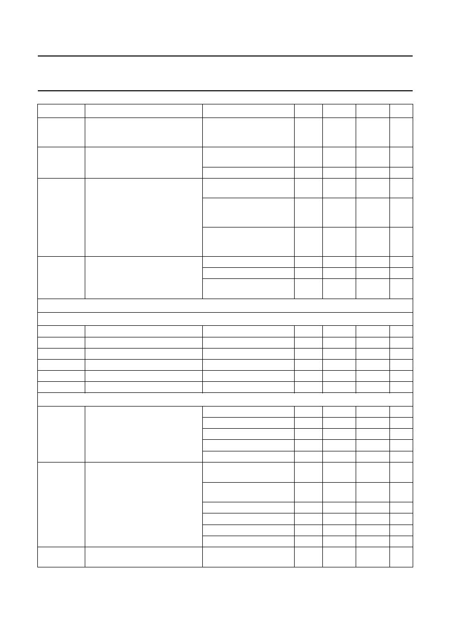
V
i(stab)(p-p)
stabilized input signal
(peak-to-peak value)
0.5
0.8
1.0
V
g
m(max)
maximum transconductance
4
5
-
mA/V
Z
i
input impedance
50
-
-
k
C
i
input capacitance
-
-
10
pF
C
o
output capacitance
-
-
5
pF
E
XTERNAL REFERENCE SIGNAL
;
INPUT PIN
20
f
XTALI
input signal frequency
-
12
-
MHz
V
i(XTALI)(p-p)
input signal amplitude
(peak-to-peak value)
AC coupled
0.8
-
2
V
F
IRST CONTROL LOOP
; note 29
f
o(nom)
free-running frequency
1f
H
mode; note 30
-
15.7
-
kHz
2f
H
mode; note 30
-
31.4
-
kHz
2f
H
mode; HDTV = 1;
note 30
-
33.8
-
kHz
2f
H
mode; CDTV = 1;
note 30
-
28.5
-
kHz
f
nom
tolerance on free-running
frequency
note 30
-
-
±
1
%
f
h/cr
holding/catching range of PLL
1f
H
mode
±
0.75
±
0.8
±
0.85
kHz
2f
H
mode
±
1.5
±
1.6
±
1.7
kHz
t
line
maximum line time difference per
line
1f
H
mode
-
2
-
+2
µ
s
2f
H
mode
-
1
-
+1
µ
s
f
contr
frequency control range in
multi-sync mode
1f
H
mode
15
-
25
kHz
2f
H
mode
30
-
50
kHz
f
corr
maximum speed of frequency
correction in multi-sync mode
-
-
100
kHz/s
V
HSEL
voltage on pin HSEL
1f
H
mode
0
-
1
V
2f
H
mode; pin must be left
open circuit
4
5
5.5
V
S
ECOND CONTROL LOOP
;
PIN
14
i
/
o
control sensitivity (loop gain)
t
i
/
t
0
500
-
-
µ
s/
µ
s
k
cor
correction factor k
note 31
-
0.5
-
t
contr
control range from start of
horizontal output to mid flyback
1f
H
mode; note 32
0
-
23.6
µ
s
2f
H
mode; note 32
0
-
11.8
µ
s
t
H(shift)
horizontal shift range
1f
H
mode; 63 steps
-
±
4.5
-
µ
s
2f
H
mode; 63 steps
-
±
2.25
-
µ
s
SYMBOL
PARAMETER
CONDITIONS
MIN.
TYP.
MAX.
UNIT
2002 Jun 04
24
Philips Semiconductors
Preliminary specification
I
2
C-bus controlled TV display processors
TDA933xH series
control sensitivity for dynamic
phase compensation
1f
H
mode
-
0.4
-
µ
s/V
2f
H
mode
-
0.2
-
µ
s/V
V
i(DP)(comp)
input voltage range for dynamic
phase compensation
pin 14; note 33
1.5
4
6.5
V
Z
i
input impedance
pin 14; note 33
100
k
t
par(cor)(max)
maximum range of parallelogram
correction
1f
H
mode; end of field;
flyback width 11
µ
s;
note 34
±
0.40
±
0.50
±
0.60
µ
s
2f
H
mode; end of field;
flyback width 5.5
µ
s;
note 34
±
0.20
±
0.25
±
0.30
µ
s
t
bow(cor)(max)
maximum range of bow correction
1f
H
mode; end of field;
flyback width 11
µ
s;
note 34
±
0.40
±
0.50
±
0.60
µ
s
2f
H
mode; end of field;
flyback width 5.5
µ
s;
note 34
±
0.20
±
0.25
±
0.30
µ
s
H
ORIZONTAL FLYBACK INPUT
;
PIN
13
V
sw(HBLNK)
switching level for horizontal
blanking
0.2
0.3
0.4
V
V
sw(p2)
switching level for phase detection
3.8
4.0
4.2
V
V
i(HFB)(max)
maximum input voltage
-
-
V
P
V
Z
i
input impedance
10
-
-
M
H
ORIZONTAL OUTPUT
;
PIN
8,
OPEN COLLECTOR
; note 35
V
OL
LOW-level output voltage
I
o
= 10 mA
-
-
0.3
V
I
o(hor)
maximum allowed output current
-
-
10
mA
V
o(max)
maximum allowed output voltage
-
-
V
P
V
duty factor
V
o
= LOW (t
on
)
51.6
51.8
52.0
%
t
on
switch-on time of horizontal drive
pulse
TV mode, HDTV = 0,
ESS = 0
155
159
163
ms
t
off
switch-off time of horizontal drive
pulse
TV mode, HDTV = 0,
ESS = 0
48
50
52
ms
t
on(ess)
switch-on time for extended slow
start
TV mode, HDTV = 0,
ESS = 1
1150
1175
1200
ms
t
jitter (
)
1f
H
mode; note 36
-
1.4
-
ns
2f
H
mode; note 36
-
1.0
-
ns
S
ANDCASTLE OUTPUT
;
PIN
9; note 37
V
SCO(0)
zero level
0
0.5
1.0
V
I
sink
sink current
0.5
0.7
0.9
mA
V
o(SCO)
output voltage
during clamp pulse
4.2
4.5
4.8
V
during blanking
2.3
2.5
2.7
V
I
source
source current
0.5
0.7
0.9
mA
SYMBOL
PARAMETER
CONDITIONS
MIN.
TYP.
MAX.
UNIT
2002 Jun 04
25
Philips Semiconductors
Preliminary specification
I
2
C-bus controlled TV display processors
TDA933xH series
I
i(grd)
guard pulse input current required
to stop the blanking after a vertical
blanking period
note 38
1.0
-
3.5
mA
t
W(1)
pulse width in 1f
H
mode
clamp pulse, 22 LLC
pulses
-
3.2
-
µ
s
vertical blanking (50/60 Hz)
-
22/17
-
lines
t
W(2)
pulse width in 2f
H
mode
clamp pulse, 22 LLC
pulses
-
1.6
-
µ
s
clamp pulse, HDTV = 1,
HDCL = 1, 18 LLC; see
Fig.11
-
1.22
-
µ
s
vertical blanking;
depends on VWAIT setting;
see Fig.13
-
-
t
d(bk-HD)
delay between start H
D
pulse and
start of clamp pulse
1f
H
mode, 37 LLC pulses
-
5.4
-
µ
s
2f
H
mode, 37 LLC pulses
-
2.7
-
µ
s
2f
H
mode, HDCL = 1,
14 LLC pulses, see Fig.11
-
0.94
-
µ
s
Vertical synchronization and geometry processing
V
D
INPUT SIGNAL
;
PIN
23
V
IL
LOW-level of input voltage
-
-
0.8
V
V
IH
HIGH-level of input voltage
2.0
-
5.5
V
I
i(VD)
input current
-
10
-
+10
µ
A
t
r(VD)
rise time
-
-
100
ns
t
f(VD)
fall time
-
-
100
ns
t
W(VD)
pulse width
0.5
-
63.5
lines
V
ERTICAL DIVIDER AND RAMP GENERATOR
;
PINS
15
AND
16; note 39
N
h
number of lines per field
(VGA mode is valid only for
TDA9331H and TDA9332H)
1f
H
TV mode
244
-
511.5
lines
1f
H
VGA mode
175
-
450
lines
2f
H
; 2f
V
; TV mode
244
-
511.5
lines
2f
H
; 1f
V
; TV mode
488
-
1023.5
lines
2f
H
VGA mode
350
-
900
lines
N
h(nom)
divider value when not locked
(number of lines per field)
(VGA mode is valid only for
TDA9331H and TDA9332H)
1f
H
or 2f
H
; 2f
V
; TV mode;
VFF = 0
-
312.5
-
lines
1f
H
or 2f
H
; 2f
V
; TV mode;
VFF = 1
-
262.5
-
lines
2f
H
; 1f
V
; TV mode; VFF = 0
-
625
-
lines
2f
H
; 1f
V
; TV mode; VFF = 1
-
525
-
lines
1f
H
; VGA mode
-
288
-
lines
2f
H
; VGA mode
-
576
-
lines
V
saw(p-p)
sawtooth amplitude
(peak-to-peak value)
VS = 1FH;
C = 100 nF; R = 39 k
-
3.0
-
V
SYMBOL
PARAMETER
CONDITIONS
MIN.
TYP.
MAX.
UNIT

2002 Jun 04
26
Philips Semiconductors
Preliminary specification
I
2
C-bus controlled TV display processors
TDA933xH series
I
dch
discharge current
-
1.2
-
mA
I
ch(ext)(R)
charge current set by external
resistor
R = 39 k
; VS = 1FH;
SVF = 0
-
16
-
µ
A
R = 39 k
; VS = 1FH;
SVF = 1
-
32
-
µ
A
Slope
vert
vertical slope
control range (63 steps)
-
20
-
+20
%
I
ch
charge current increase
60/50 Hz or 120/100 Hz
18.0
19.0
20.0
%
V
rampL
LOW-voltage level of ramp
-
2.3
-
V
V
ERTICAL DRIVE OUTPUTS
;
PINS
1
AND
2
I
o(ver)(p-p)
differential output current
(peak-to-peak value)
VA = 1FH
0.88
0.95
1.02
mA
I
CM
common mode current
360
400
440
µ
A
V
o(VDO)
output voltage range
0
-
4.0
V
Lin
vert
vertical linearity
upper/lower ratio; note 40
0.98
1.00
1.02
D
E
-
INTERLACE
D
1stfld
first field delay
DIP = 0; note 41
-
0.5H
-
E-W
WIDTH
; note 42
CR
control range
63 steps
100
-
65
%
I
o(eq)
equivalent output current
VGA = 0; note 42
0
-
700
µ
A
V
o(EW)
E-W output voltage range
1.0
-
8.0
V
I
o(EW)
E-W output current range
0
-
1200
µ
A
E-W
PARABOLA
/
WIDTH
CR
control range
63 steps
-
42
-
+14
%
I
o(eq)
equivalent output current
E-W = 3FH
-
185
-
+62
µ
A
I
2
C
cc
I
2
C-bus setting for zero corner
correction
-
16 DEC
-
E-W
CORNER
/
PARABOLA
CR
control range
63 steps
-
42
-
+14
%
I
o(eq)
equivalent output current
PW = 3FH; E-W = 3FH
-
185
-
+62
µ
A
I
2
C
cc
I
2
C-bus setting for zero corner
correction
-
16 DEC
-
E-W
TRAPEZIUM
CR
control range
63 steps
-
5
-
+5
%
I
o(eq)
equivalent output current
-
100
-
+100
µ
A
E-W EHT
TRACKING
V
i(EHTIN)
input voltage
1.2
-
2.8
V
m
scan
scan modulation range
-
7
-
+7
%
EW
sensitivity
63 steps
0
-
9
%/V
SYMBOL
PARAMETER
CONDITIONS
MIN.
TYP.
MAX.
UNIT

2002 Jun 04
27
Philips Semiconductors
Preliminary specification
I
2
C-bus controlled TV display processors
TDA933xH series
V
ERTICAL AMPLITUDE
CR
control range
63 steps; SC = 00H
80
-
120
%
I
o(eq)(diff)(p-p)
equivalent differential vertical drive
output current (peak-to-peak value)
SC = 00H
760
-
1140
µ
A
V
ERTICAL SHIFT
CR
control range
63 steps
-
5
-
+5
%
I
o(eq)(diff)(p-p)
equivalent differential vertical drive
output current (peak-to-peak value)
-
50
-
+50
µ
A
S-
CORRECTION
CR
control range
63 steps
-
8
-
+24
%
I
2
C
sc
I2C-bus setting for zero
S-correction
-
13 DEC
-
V
ERTICAL
EHT
TRACKING
/
OVERVOLTAGE PROTECTION
V
i
input voltage
1.2
-
2.8
V
m
scan
scan modulation range
±
4.5
±
5
±
5.5
%
vert
vertical sensitivity
5.7
6.3
6.9
%/V
I
o(eq)(EW)
EW equivalent output current
+100
-
-
100
µ
A
V
ov(det)
overvoltage detection level
note 43
3.7
3.9
4.1
V
V
ERTICAL ZOOM MODE
(
OUTPUT CURRENT VARIATION WITH RESPECT TO NOMINAL SCAN
); note 44
F
zoom
vertical zoom factor
63 steps
0.75
-
1.38
F
lim
output current limiting and RGB
blanking
1.01
1.05
1.08
V
ERTICAL SCROLL
; note 45
CR
control range (percentage of
nominal picture amplitude)
63 steps
-
18
-
+19
%
V
ERTICAL WAIT
; note 46
t
d(scan)
delay of start vertical scan
23 steps
8
-
31
lines
F
LASH DETECTION INPUT
;
PIN
5; note 43
V
i(FLASH)
input voltage range
0
-
V
P
V
V
FLASH(det)
voltage detection level
-
2
-
V
V
det(hys)
detection level hysteresis
-
0.2
-
V
t
W(FLASH)
pulse width
200
-
-
ns
I
2
C-bus control inputs/outputs; pins 10 and 11
V
IL
LOW-level input voltage
-
-
1.5
V
V
IH
HIGH-level input voltage
3.5
-
5.5
V
I
IL
LOW-level input current
V
IL
= 0 V
-
0
-
µ
A
I
IH
HIGH-level input current
V
IH
= 5.5 V
-
0
-
µ
A
V
OL
LOW-level output voltage
SDA; I
OL
= 6 mA
-
-
0.6
V
SYMBOL
PARAMETER
CONDITIONS
MIN.
TYP.
MAX.
UNIT

2002 Jun 04
28
Philips Semiconductors
Preliminary specification
I
2
C-bus controlled TV display processors
TDA933xH series
Notes
1. The normal operation of the IC is guaranteed for a supply voltage between 7.2 and 8.8 V. When the supply voltage
drops below the POR level, status bit POR is set and the horizontal output is switched off. When the supply voltage
is between 7.2 V and the POR level, the horizontal frequency is kept in the specified holding range.
2. For the low power start-up mode, a voltage of 5 V has to be supplied to pin 22. The current that is required for this
function is about 3.0 mA. After the start-up voltage is applied, the signal at the horizontal drive output will have
nominal t
off
, while t
on
grows gradually from zero to about 30% of the nominal value, resulting in a line frequency of
approximately 50 kHz (2fH) or 25 kHz (1fH). The start-up mode is continued as soon as the main supply voltage is
switched on and the I
2
C-bus data has been received. After status bit POR has been read out, bits STB must be set
to 1 within 24 ms, to continue slow start. If bits STB are not sent within 24 ms, the horizontal output will be
automatically switched off via slow stop. It is also possible to first set bits STB to 1, before reading bit POR. Start-up
of the horizontal output will then continue 24 ms after bit POR is read. When the main supply is present, the 5 V
supply on pin 22 can be removed. If low power start-up is not used, pin 22 should be connected to ground. More
information can be found in the application report.
3. The RGB to YUV matrix on the RGB-1 input is the inverse of the YUV to RGB matrix for PAL. For a one-on-one
transfer of all three channels from the RGB-1 input to the RGB output, the PAL colour difference matrix should be
selected (MAT = 0, MUS = 0).
4. The colorimetry that is used for high definition ATSC signals is described in document ANSI/SMPTE 274M-1995.
The formula to compute the luminance signal from the RGB primary components differs from the formula that is used
for the PAL system. The consequence is that a different matrix is needed to calculate the internal G
-
Y signal from
the R
-
Y and B
-
Y signals, see the formulas below:
The G
-
Y signal can be derived from the formula for Y:
ATSC signals are transmitted as YP
B
P
R
signals. The colour-difference components P
B
and P
R
are amplitude
corrected versions of B
-
Y and R
-
Y:
DAC
OUTPUT
;
PIN
25; note 47
V
o(min)
minimum output voltage
0.15
0.3
0.4
V
V
o(max)
maximum output voltage
3.7
4.0
4.3
Z
o
output impedance
note 47
0.3
-
10
k
I
o
output current
-
-
2
mA
SYMBOL
PARAMETER
CONDITIONS
MIN.
TYP.
MAX.
UNIT
Y
0.2126R
0.7152G
0.0722B
+
+
=
R
Y
≠
0.7874R
0.7152G
≠
0.0722B
1.575 maximum amplitude
(
)
≠
=
B
Y
≠
0.2126R
≠
0.7152G
≠
0.9278B
1.856 maximum amplitude
(
)
+
=
G
Y
≠
0.2973
≠
R
Y
≠
(
)
0.1010 B
Y
≠
(
)
≠
=
P
B
0.5 B
Y
≠
(
)
1
0.0722
≠
---------------------------
B
Y
≠
(
)
1.856
------------------
=
=
P
R
0.5 R
Y
≠
(
)
1
0.2126
≠
----------------------------
R
Y
≠
(
)
1.575
-------------------
=
=

2002 Jun 04
29
Philips Semiconductors
Preliminary specification
I
2
C-bus controlled TV display processors
TDA933xH series
Note that the "YUV" input of the TDA933xH is actually a Y,
-
(R
-
Y) and
-
(B
-
Y) input. When the TV set has an input
for a YPBPR signal with amplitudes of 0.7 V for all three components, the signals should be amplified to Y,
-
(B
-
Y)
and
-
(R
-
Y) signals as follows:
5. This parameter is not tested during production but is guaranteed by the design and qualified by means of matrix
batches which are made in the pilot production period.
6. The inputs for RGB-1 and RGB-2 insertion (pins 33 and 38) both supply a small source current to the pins. If the pins
are left open circuit, the input voltage will rise above the insertion switching level.
7. This parameter is measured at nominal settings of the various controls.
8. The switching of the OSD (RGB-2) input has two modes, which can be selected via the I
2
C-bus:
a) Fast switching between the OSD signal and the internal RGB signals.
b) Blending (fading) function between the OSD signal and the internal RGB signals. The blending control curve is
given in Fig.4. The blender input is optimized for the blender output of the SAA5800 (ArtistIC).
9. The saturation, contrast and brightness controls are active on the YUV signals and on the first RGB input signals.
Nominal contrast is specified with the contrast DAC in position 32 DEC, nominal saturation with the saturation DAC
in position 22 DEC. The second RGB input (which is intended to be used for OSD and teletext display) can only be
controlled on brightness.
10. For video signals with a black level that deviates from the back-porch blanking level, the signal is `stretched' to the
blanking level. The amount of correction depends on the IRE value of the signal (see Fig.8). The black level is
detected by means of an internal capacitor. The black level stretcher can be switched on and off via bit BKS in the
I
2
C-bus. The values given in the specification are valid only when the luminance input signal has an amplitude of
1 V (b-w).
11. Because of the 2-point black current stabilization circuit, both the black level and the amplitude of the RGB output
signals depend on the drive characteristic of the picture tube. The system checks whether the returning measuring
currents meet the requirement and adapts the output level and gain of the circuit as necessary. Therefore, the typical
values of the black level and amplitude at the output are just given as an indication for the design of the RGB output
stage.
a) The 2-point black level system adapts the drive voltage for each cathode such that the two measuring currents
have the right value. The consequence is that a change in the gain of the output stage will be compensated by a
gain change of the RGB control circuit. Because different picture tubes may require different drive voltage
amplitudes, the ratio between the output signal amplitude and the inserted measuring pulses can be adapted via
the I
2
C-bus. This is indicated in the parameter `Adjustment range of RGB drive levels'.
b) Because of the dependence of the output signal amplitude on the application, the peak-white and soft-clipping
limiting levels have been related to the input signal amplitude.
c) The signal amplitude at the RGB outputs of the TDA933xH depends on the gain of the RGB amplifiers. The gain
of the RGB amplifiers should be 35 to get the nominal signal amplitude of 2 V (b-w) at the RGB outputs for a
cathode drive level of 70 V (b-w) and the nominal setting of the drive level bits (CL
3210
= 1000, see Table 15).
12. The bandwidth of the video channels depends on the capacitive load at the RGB outputs. For 2f
H
or VGA
applications, external (PNP) emitter followers on the RGB outputs of the TDA933xH are required, to avoid reduction
of the bandwidth by the capacitance of the wiring between the TDA933xH and the RGB power amplifiers on the
picture tube panel. If emitter followers are used, it should be possible to obtain the bandwidth figures that are
mentioned for 10 pF load capacitance.
Y
in,IC
1
0.7
--------
Y
in,TV
◊
1.43Y
in,TV
=
=
B
Y
≠
(
)
≠
in,IC
1.856
0.7
---------------
P
Bin TV
,
◊
2.65
≠
P
B in,TV
=
=
R
Y
≠
(
)
≠
in,IC
1.575
0.7
---------------
P
Rin TV
,
◊
2.25
≠
P
R in,TV
=
=

2002 Jun 04
30
Philips Semiconductors
Preliminary specification
I
2
C-bus controlled TV display processors
TDA933xH series
13. The timing of the horizontal blanking pulse on the RGB outputs is illustrated in Fig.10.
a) The start of the blanking pulse is determined by an internal counter blanking that starts 40 LLC (line locked clock)
pulses before the centre of the horizontal flyback pulse. This is 5.8
µ
s for 1fH and 2.9
µ
s for 2fH TV mode. The
end of the blanking is determined by the trailing edge of the flyback pulse. If required, the start of the counter
blanking can be adjusted in 15 steps with bus bits LBL3 to LBL0. This can be useful when HDTV or VGA signals
are applied to the IC.
b) When the reproduction of 4 : 3 pictures on a 16 : 9 picture tube is realized by reducing the horizontal scan
amplitude, the edges of the picture may be slightly disturbed. This effect can be prevented by adding an additional
blanking pulse to the RGB signals. This blanking pulse is derived from the horizontal oscillator and is directly
related to the incoming H
D
pulse (independent of the flyback pulse). The additional blanking pulse overlaps the
normal blanking signal by approximately 1
µ
s (1f
H
) or 0.5
µ
s (2f
H
) on both sides. This wide blanking is activated
by bit HBL. The phase of this blanking can be controlled in 15 steps by bits HB3 to HB0.
14. When a YUV or RGB signal is applied to the IC and no separate horizontal or vertical timing pulses are available, an
external sync separator circuit is needed. The TDA933xH has an edge triggered phase detector circuit on the H
D
input that uses the start of the H
D
pulse as timing reference. To avoid horizontal phase disturbances during the
vertical blanking period, it is important that the sync separator does not generate extra horizontal sync pulses during
the vertical sync pulse on the video signal.
15. Start-up behaviour of the CCC loop. After the horizontal output is released via bits STB, the RGB outputs are blanked
and the CCC loop is activated. Because the picture tube is cold, the measured cathode currents are too small, and
both gain and offset are set at the maximum value so that the CCC loop gets out of range and status bit BCF is set
to 1. Once the picture tube is warm, the loop comes within range and the set signal for bit BCF is removed. Status
bit BCF is set if the voltage of at least one of the cut-off measurement lines at the RGB outputs is lower than 1.5 V
or higher than 3.5 V. The RGB outputs are unblanked as soon as bit BCF changes from 1 to 0. To avoid a bright
picture after switch-on with a warm picture tube, reset of bit BCF is disabled for 0.5 s after switch-on of the horizontal
output. If required, the blanking period of the RGB outputs can be increased by forcing the blanking level at the RGB
outputs via RBL = 1. When status bit BCF changes from 1 to 0, bit RBL can be set to 0 after a certain waiting period.
16. Voltage V
g2
of the picture tube can be aligned with the help of status bits WBC and HBC. Bit WBC becomes 1 if the
lowest of the three RGB output voltages during the cut-off measurement lines is within the alignment window of
±
0.1 V around 2.5 V. Bit HBC is 0 if the lowest cut-off level is below 2.6 V, and 1 if this level is above 2.6 V.
a) Voltage V
g2
should be aligned such that bit WBC becomes 1. If bit WBC is 0, bit HBC indicates in which direction
voltage V
g2
should be adjusted. If bit HBC = 0, the DC level at the RGB outputs of the IC is too low and voltage
V
g2
should be adjusted lower until bit WBC becomes 1. If HBC = 1, the DC level is too high and voltage V
g2
should
be adjusted higher until bit WBC becomes 1.
b) It should be noted that bit WBC is only meant for factory alignment of voltage V
g2
. If the value of bit WBC depends
on the video content, this is not a problem. Correct operation of the black current loop is guaranteed as long as
status bit BCF = 0, meaning that the DC level of the measurement lines at the RGB outputs of the IC is between
1.5 and 3.5 V.
17. Signal-to-noise ratio (S/N) is specified as a peak-to-peak signal with respect to RMS noise (bandwidth 10 MHz).
18. This is a current input. When the black current feedback loop is closed (only during measurement lines or during fixed
beam current switch off), the voltage at this pin is clamped at 3.3 V. When the loop is open circuit, the input is not
clamped and the maximum sink current is approximately 100
µ
A. The voltage on the pin must not exceed the supply
voltage.

2002 Jun 04
31
Philips Semiconductors
Preliminary specification
I
2
C-bus controlled TV display processors
TDA933xH series
19. The control circuit contains a PWL circuit and a soft clipper.
a) The detection level of the PWL can be adjusted via the I
2
C-bus in a control range between 0.65 and 1.0 V (b-w).
This amplitude is related to the Y input signal, typical amplitude 1 V (b-w), at maximum contrast setting. The
detector measures the amplitude of the RGB signals after the contrast control. The output signal of the PWL
detector is filtered by an external capacitor, so that short transients in the video signal do not activate the limiting
action. Because the capacitor is externally available at pin 34, the set maker can adapt the filter time constant as
required. The contrast reduction of the PWL is obtained by discharging the external capacitor at the beam current
limiting input (pin 43). To avoid the PWL circuit from reducing the contrast of the main picture when the amplitude
of the inserted RGB2 signal is too high, the output current of the PWL detector is disabled when the fast blanking
input (pin 38) is high. In blending mode (OBL = 1), the PWL detector is disabled when the blending voltage is
above the 50% insertion level. The soft clipper circuit will still limit the peak voltage at the RGB outputs.
b) In addition to the PWL circuit, the IC contains a soft clipper function which limits short transients that exceed the
PWL. The difference between the PWL and the soft clipping level can be adjusted between 0 and 10% in
three steps via the I
2
C-bus, with bus bits SC1 and SC0 (soft clipping level equal or higher than the PWL). It is
also possible to switch off the soft clipping function.
20. The above-mentioned output amplitude range at which the PWL detector is activated is valid for nominal settings of
the white point controls, and when the CCC loop is switched off or set to 1-point stabilization mode. In 2-point
stabilization mode, the mentioned range is only valid when the gain of the RGB output stages is dimensioned such
that the RGB output amplitudes are 2 V (b-w) for nominal contrast setting, see also note 11.
21. The soft clipper gain reduction is measured by applying a sawtooth signal with rising slope and 1 V (b-w) at the
luminance input. To prevent the beam current limiter from operating, a DC voltage of 3.5 V must be applied to pin 43.
The contrast is set at the maximum value, the PWL at the minimum value, and the soft clipping level is set at 0%
above the PWL (SC
10
= 00). The tangents of the sawtooth waveform at one of the RGB outputs is now determined
at the beginning and end of the sawtooth. The soft clipper gain reduction is defined as the ratio of the slopes of the
tangents for black and white, see Fig.9.
22. When the blue stretch function is activated (via I
2
C-bus bit BLS), the gain of the red and green channels is reduced
for input signals that exceed a value of 80% of the nominal amplitude. The result is that the white point is shifted to
a higher colour temperature.
23. Switch-off behaviour of TDA933xH. For applications with an EHT generator without bleeder resistor, the picture tube
capacitance can be discharged with a fixed beam current when the set is switched off. The magnitude of the
discharge current is controlled via the black current loop. The fixed beam current mode can be activated with bit FBC.
With the fixed beam current option activated, it is still possible to have a black screen during switch-off. This is
realized by placing the vertical deflection in the overscan position. This mode is activated by bit OSO. There are two
possible situations for switch-off (see notes 24 and 25).
24. The set is switched to standby via the I
2
C-bus. In this situation, the procedure is as follows:
a) Vertical scan is completed.
b) Vertical flyback is completed.
c) Slow stop of the horizontal output is started, by gradually reducing the `on-time' at the horizontal output from
nominal to zero.
d) At the same moment, the fixed beam current is forced via the black current loop (if FBC = 1).
e) If OSO = 1, the vertical deflection stays in overscan position; if OSO = 0, the vertical deflection keeps running.
f) The slow stop time is approximately 50 ms, the fixed beam current flows for 18.6 ms or 25 ms, depending on the
value of bit TFBC, see Fig.15.
g) To avoid the fixed beam current being activated when the horizontal output has stopped, the fixed beam current
cannot be activated anymore via the FBCSO pin; see the following note.

2002 Jun 04
32
Philips Semiconductors
Preliminary specification
I
2
C-bus controlled TV display processors
TDA933xH series
25. The set is switched off via the mains power switch. When the mains supply is switched off, the supply voltage of the
line deflection circuit of the TV set will decrease. A detection circuit must be made that monitors this supply voltage.
When the supply voltage suddenly decreases, pin FBCSO (fixed beam current switch-off) of the TDA933xH must be
pulled high. In this situation, the procedure is as follows:
a) Vertical scan is completed.
b) Vertical flyback is completed.
c) The fixed beam current is forced via the black current loop (if FBC = 1). The horizontal output keeps running.
As the supply voltage for the line transformer decreases, the EHT voltage will also decrease.
d) If OSO = 1, the vertical deflection stays in overscan position; if OSO = 0, the vertical deflection keeps running.
e) When the supply voltage of the TDA933xH drops below the POR level, horizontal output and fixed beam current
are stopped.
26. The discharge current for the picture tube can be increased with an external current division circuit on the black
current input (pin 44). The current division should only be active for high cathode currents, so that the operation of
the black current stabilization loop is not affected. When the feedback current supplied to pin 44 is less than 1mA,
the DC level at the RGB outputs will go to the maximum value of 6.0 V (2-point black current stabilization) or 5.6 V
(1-point or no black current stabilization).
27. A stable switching of the H
D
input is realized by using a Schmitt trigger input.
28. The simplified circuit diagram of the oscillator is given in Fig.3. To ensure that the oscillator will start-up, the ceramic
resonator must fulfil the following condition:
.
Example: When the resonator is loaded with 60 pF (this is a typical value for a 12 MHz resonator), the series
resistance of the resonator must be smaller than 30
.
A suitable ceramic resonator for use with the TDA933xH is the Murata CST12.0MT, which has built-in load
capacitances C
a
and C
b
. For higher accuracy, it is also possible to use a quartz crystal, which is even less critical
with respect to start-up because of its lower load capacitance.
29. Pin HSEL must be connected to ground in a 1f
H
application; it must be left open circuit for a 2f
H
application. The
TDA9331H and TDA9332H can be switched to a multi-sync mode, in which the horizontal frequency can vary
between 15 and 25 kHz (1f
H
mode) or 30 and 50 kHz (2f
H
mode).
30. The indicated tolerance on the free-running frequency is only valid when an accurate reference frequency (obtained
with an accurate 12 MHz crystal) is used. The tolerance of the reference resonator must be added to obtain the real
tolerance on the free-running frequency.
31. The correction factor k of the phase-2 loop is defined as the amount of correction per line period of a phase error
between the horizontal flyback pulse and the internal phase-2 reference pulse. When k = 0.5, the phase error
between the flyback pulse and the internal reference is halved each line period.
32. The control range of the second control loop depends on the line frequency. The maximum control range from the
rising edge of HOUT to the centre of the flyback pulse is always 37% of one line period, for the centre position of the
dynamic phase compensation (4.0 V at pin 14).
33. The dynamic phase compensation input (pin 14) is connected to an internal reference voltage of 4.0 V via a resistor
of 100 k
. If dynamic phase compensation is not used, this pin should be decoupled to ground (pin 19) via a
capacitor of 100 nF.
34. The range of parallelogram and bow correction is proportional to the width of the horizontal flyback pulse. For zero
correction, use DAC setting 7 DEC or 0111 (bin). The effect of the corrections is shown in Fig.16.
C
L
2
R
i
1.1
◊
10
19
≠
◊

2002 Jun 04
33
Philips Semiconductors
Preliminary specification
I
2
C-bus controlled TV display processors
TDA933xH series
35. For safe operation of the horizontal output transistor and to obtain a controlled switch-on time of the EHT, the
horizontal drive starts up in a slow start mode. The horizontal drive starts with a very short `on-time' of the horizontal
output transistor (line locked clock pulse, i.e. 72 ns), the `off-time' of the transistor is identical to the `off-time' in normal
operation. The starting frequency during switch-on is therefore approximately twice the normal value. The t
on
is
slowly increased to the nominal value in approximately 160 ms (see Fig.15). When the nominal frequency is reached,
the PLL is closed such that only very small phase corrections are necessary. This ensures safe operation of the
output stage.
a) For picture tubes with Dynamic Astigmatic Focusing (DAF) guns, the rise of the EHT voltage between
75 and 100% is preferred to be even slower than the rise time from 0 to 75%. This can be realized by activating
bit ESS, at which the total switch-on time of the horizontal output pulse is approximately 1175 ms.
b) During switch-off, the slow-stop function is active. This is realized by decreasing the t
on
of the output transistor
complementary to the start-up behaviour. The switch-off time is approximately 50 ms. The slow-stop procedure
is synchronized to the start of the first new vertical field after reception of the switch-off command. During the
slow-stop period, the fixed beam current switch-off can be activated (see also note 23). This current is active
during a part of the slow stop period, see Fig.15.
c) The horizontal output is gated with the flyback pulse so that the horizontal output transistor cannot be switched
on during the flyback pulse. This protection is not active during the switch-on or switch-off period.
36. This parameter is not tested during production and is just given as application information for the designer of the
television receiver.
37. The rise and fall times of the blanking pulse and clamping pulse at the sandcastle output (pin 9) depend on the
capacitive load. The value of the source current during the rising edge or sink current during the falling edge is
0.7 mA (typical value).
38. The vertical guard pulse from the vertical output stage should be connected to pin 9 which acts as a current sense
input. The guard pulse should fall within the vertical blanking period (see Figs 12 and 13) and should have a width
of at least one line period. The guard current value should be at least 1 mA.
39. Switching between the 1f
V
or the 2f
V
mode is realized via bit SVF.
40. The vertical linearity is measured on the differential output current at the vertical drive output (pins 1 and 2) for zero
S-correction. The linearity is defined as the ratio of the upper and lower half amplitudes at the vertical output. The
upper amplitude is measured between lines 27 and 167, the lower amplitude between lines 167 and 307 for a 50 Hz
video signal.
41. The field detection mechanism is explained in Fig.17.
a) The incoming V
D
pulse is synchronized with the internal clock signal CK2H that is locked to the incoming H
D
pulse. If the synchronized V
D
pulse of a field coincides with the internally generated horizontal blanking signal
HBLNK, then this is field 1. If the synchronized V
D
pulse does not coincide with HBLNK, then this is field 2. Signals
CK2H and HBLNK are both output signals of the horizontal divider circuit that is part of the line-locked clock
generator. A reliable field detection is important for correct interlacing and de-interlacing and for the correct timing
of the measurement lines of the black current loop. For the best noise margin, the edges of the V
D
pulse should
be on approximately
1
/
4
and
3
/
4
of the line, referred to the rising edges of the H
D
input signal.
b) If bus bit VSR = 0, the end of the V
D
pulse is used as reference for both field detection and start of vertical scan.
If VSR = 1, the starting edge is used.
42. Output range percentages mentioned for E-W control parameters are based on the assumption that the E-W
modulator is dimensioned such that 400
µ
A variation in E-W output current of the IC is equivalent to 20% variation
in picture width. In VGA mode, the E-W output current is proportional to the applied line frequency.

2002 Jun 04
34
Philips Semiconductors
Preliminary specification
I
2
C-bus controlled TV display processors
TDA933xH series
43. The IC has protection inputs for flash protection and overvoltage protection.
a) The flash protection input is used to switch the horizontal drive output off immediately if a picture tube flashover
occurs, to protect the line output transistor. An external flash detection circuit is needed. When the flash input is
pulled HIGH, the horizontal output is switched off and status bit FLS is set. When the input turns LOW again, the
horizontal output is switched on immediately without I
2
C-bus intervention via the slow start procedure.
b) The overvoltage (X-ray) protection is combined with the EHT compensation input. When this protection is
activated, the horizontal drive can be directly switched off (via the slow stop procedure). It is also possible to
continue the horizontal drive and only set status bit XPR in output byte 01 of the I
2
C-bus. The choice between the
two modes of operation is made via bit PRD.
44. The ICs have a zoom adjustment possibility for the horizontal and vertical deflection. For this reason, an extra DAC
is included in the vertical amplitude control, which controls the vertical scan amplitude between 0.75 and 1.38 of the
nominal scan. At an amplitude of 1.05 times the nominal scan, the output current is limited and the blanking of the
RGB outputs is activated, see Fig.14. In addition to the variation of the vertical amplitude, the picture can be vertically
shifted on the screen via the `scroll' function. The nominal scan height must be adjusted at a position of 19H (25 DEC)
of the vertical `zoom' DAC and 1FH (31 DEC) for the vertical `scroll' DAC.
45. The vertical scroll function is active only in the expand mode of the vertical zoom, i.e. at a DAC position larger
than 10H (16 DEC).
46. With the vertical wait function, the start of the vertical scan can be delayed with respect to the incoming vertical sync
pulse. The operation is different for the various scan modes, see Table 55 and Figs 12 and 13. The minimum value
for the vertical wait is 8 line periods. If the setting is lower than 8, the wait period will remain 8 line periods.
47. In the TDA9330H and TDA9332H, the DAC output is I
2
C-bus controlled. In the TDA9331H, the DAC output voltage
is proportional to the centre frequency of the line-oscillator. In TV mode, the output voltage will always be at the
minimum value. In VGA mode, the output is at the minimum value for the lowest centre frequency (32 kHz) and at
the maximum value for the highest centre frequency (48 kHz). The output impedance of the DAC output depends on
the output voltage. The output consists of an emitter follower with an internal resistor of 50 k
to ground.
Table 55 Operation of the vertical wait function
MODE
START OF VERTICAL SCAN
1f
H
; TV mode
fixed; see Fig.12
2f
H
; TV mode; VSR = 0
end of V
D
plus vertical wait setting
2f
H
; TV mode; VSR = 1
start of V
D
plus vertical wait setting
1f
H
; multi sync mode
start of V
D
plus vertical wait setting
2f
H
; multi sync mode
start of V
D
plus vertical wait setting
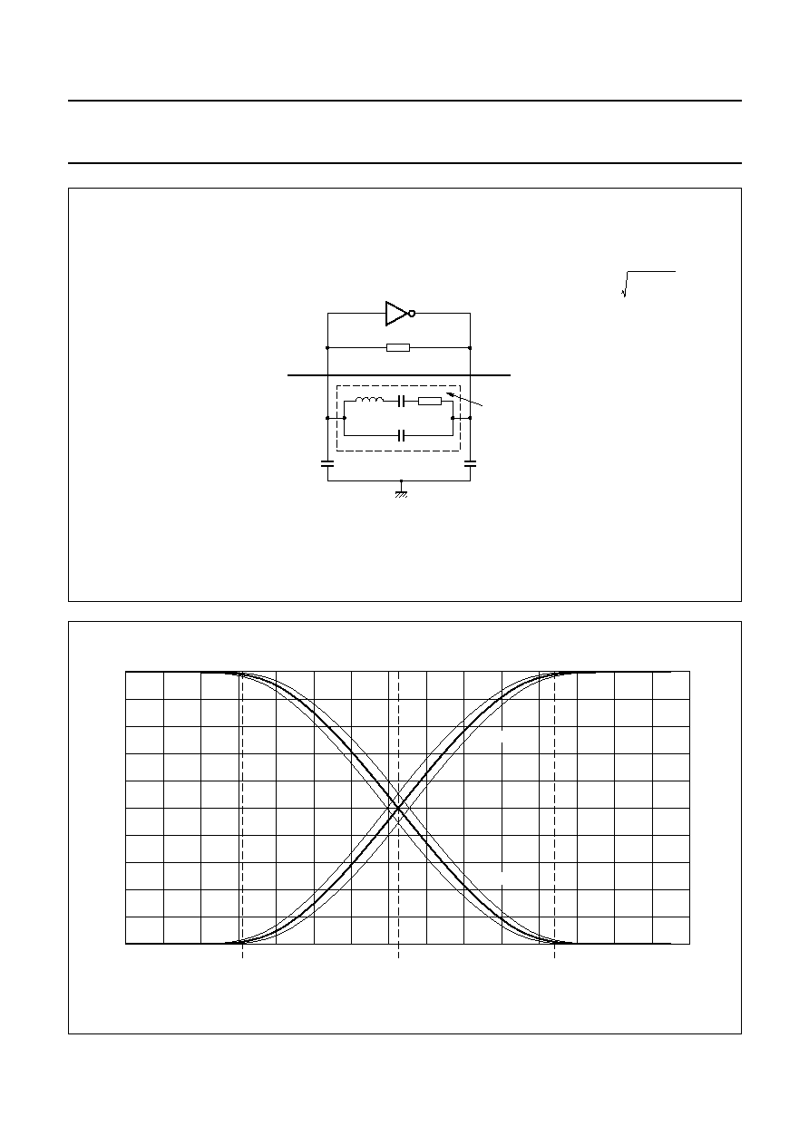
2002 Jun 04
35
Philips Semiconductors
Preliminary specification
I
2
C-bus controlled TV display processors
TDA933xH series
handbook, halfpage
MGR447
100 k
XTALI
XTALO
crystal
or
ceramic
resonator
Ri
Li
Ci
Ci
gm
Cp
Ca
Cb
Fig.3 Simplified diagram of crystal oscillator.
f
osc
1
L
i
C
i
C
L
◊
C
i
C
L
+
-------------------
◊
2
-------------------------------------
=
C
L
C
p
C
a
C
b
◊
C
a
C
b
+
--------------------
+
=
Requirement for start-up:
C
2
L
R
i
1.1
10
19
≠
◊
◊
handbook, full pagewidth
100
0
0
1.0
1.4
0.4
0.31
0.8
1.2
0.2
0.725
1.14
0.6
20
40
60
80
MGR448
Vinsert (V)
blending
(%)
external
internal
Fig.4 Blending characteristic (typical curve and minimum/maximum limits).

2002 Jun 04
36
Philips Semiconductors
Preliminary specification
I
2
C-bus controlled TV display processors
TDA933xH series
handbook, halfpage
300
100
0
200
MGS892
0
20
40
80
60
DAC (decimal value)
(%)
Fig.5 Saturation control curve.
handbook, halfpage
0
20
40
80
200
0
160
MGS893
60
120
80
40
DAC (decimal value)
(%)
Fig.6 Contrast control curve.
handbook, halfpage
0
20
40
80
1
0.5
MGS894
60
0
-
0.5
-
1
DAC (decimal value)
(V)
Fig.7 Brightness control curve.
Conditions: settings for cathode drive and white point nominal;
gain of RGB amplifiers such that the amplitude at the RGB
outputs is 2 V (b-w); relative to cutoff level.
handbook, halfpage
0
40
80
120
100
20
-
20
60
80
0
40
MGR452
output
(IRE)
input (IRE)
A
A
B
B
A-to-A: maximum black level shift.
B-to-B: level shift at 15% of peak white.
Fig.8 I/O relation of black level stretch circuit.
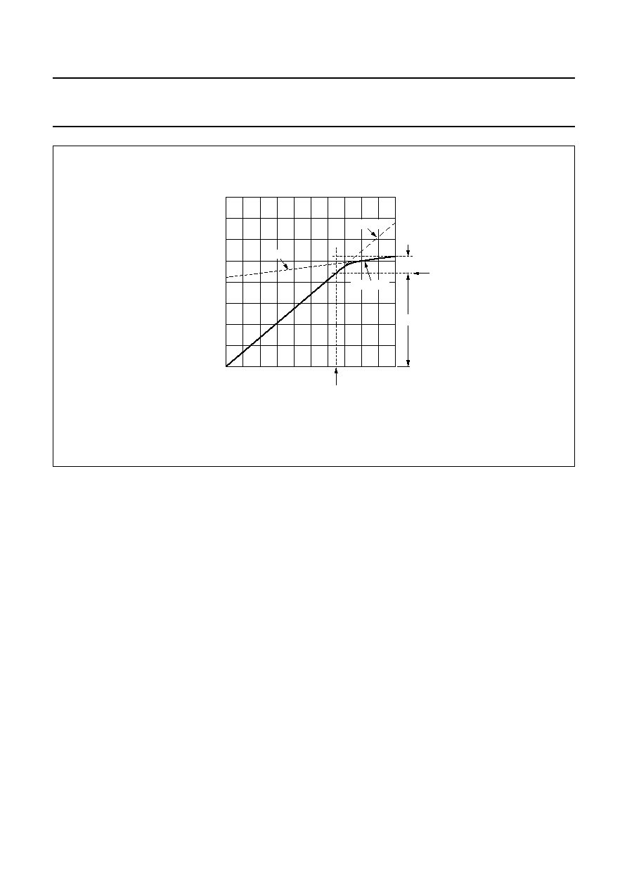
2002 Jun 04
37
Philips Semiconductors
Preliminary specification
I
2
C-bus controlled TV display processors
TDA933xH series
handbook, full pagewidth
0
4
2
3
1
0
20
Vo(RGB)(b-w)
(V)
100
MGS895
40
60
80
YIN (IRE)
tangent
clipper off
clipper on
PWL
input level
PWL
output level
A
B
Fig.9 Soft clipper characteristic.

2002 Jun 04
38
Philips Semiconductors
Preliminary specification
I
2
C-bus controlled TV display processors
TDA933xH series
handbook, full pagewidth
MGS896
HD input pulse
wide blanking
(if HBL = 1)
horizontal
flyback pulse
flyback blanking
counter blanking
video blanking
phase slicing level (4 V)
blanking slicing level (0.3 V)
reference phi1
reference phi2
HSHIFT
0 to 63 LLC
101 LLC
40 LLC
(2)
(1)
Fig.10 Timing of horizontal blanking (1 line period is 440 LLC pulses).
1) Position of wide blanking can be adjusted with bus bits HB3 to HB0.
2) Start of line blanking can be adjusted with bus bits LBL3 to LBL0.

2002 Jun 04
39
Philips Semiconductors
Preliminary specification
I
2
C-bus controlled TV display processors
TDA933xH series
handbook, full pagewidth
MGS897
0.75
µ
s
2.35
µ
s
2.40
µ
s
5.5
µ
s
mid blank = mid flyback
37 LLC = 2.67
µ
s
22 LLC = 1.59
µ
s
HD input
HSHIFT
2 fH NTSC
signal
(fH = 31.47 kHz)
CLP pulse
counter
blanking
0.606
µ
s
0.592
µ
s
1.993
µ
s
3.784
µ
s
50 ns
mid blank = mid flyback
18 LLC = 1.22
µ
s
HD input
HDTV
signal
(fH = 33.75 kHz)
CLP pulse
0.592
µ
s
15 LLC = 1.01
µ
s
counter
blanking
(a) Timing in 2 fH TV mode (HDTV = 0, HDCL = 0)
(b) Timing in HDTV mode (HDTV = 1, HDCL = 1)
HSHIFT
40 LLC = 2.69
µ
s
+
14 LLC
-
16 LLC
40 LLC = 2.89
µ
s
+
14 LLC
-
16 LLC
Fig.11 Timing of clamp pulse and line blanking in 2f
H
TV mode and HDTV mode.
Video signals are shown as illustration only. All horizontal timing signals in the IC are solely related to the start of the H
D
pulse
that is applied to the IC.
All horizontal timing signals are generated with the help of the internal line locked clock (LLC). One line period is always divided
into 440 line locked clock pulses. Time periods depicted in the figure are only valid for line frequencies mentioned.
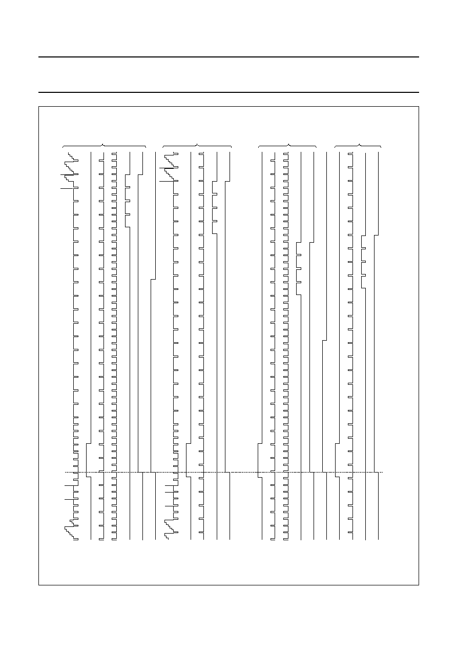
2002
Jun
04
40
Philips Semiconductors
Preliminar
y specification
I
2
C-b
us controlled TV displa
y processors
TD
A933xH ser
ies
2002
Jun
04
40
Philips Semiconductors
Preliminar
y specification
I
2
C-b
us controlled TV displa
y processors
TD
A933xH ser
ies
This text is here in white to force landscape pages to be rotated correctly when browsing through the pdf in the Acrobat reader.This text is here in
_
white to force landscape pages to be rotated correctly when browsing through the pdf in the Acrobat reader.This text is here inThis text is here in
white to force landscape pages to be rotated correctly when browsing through the pdf in the Acrobat reader. white to force landscape pages to be ...
ha
ndbook, full pagewidth
Video from
HIP
Video from
HIP
625
23
312
336
RESET LINE COUNTER
50 Hz
60 Hz
1st
field
2nd
field
1st
field
2nd
field
HD = HA
VD = VA
Reset vertical
sawtooth
Reset vertical
sawtooth
Vertical
blank
AKB pulses
HD = HA
VD = VA
AKB pulses
Vertical
blank
Internal
2fH clock
HD
HD
VD
VD
Vertical
blank
AKB pulses
Vertical
blank
AKB pulses
Internal
2fH clock
L
R
G
B
L
R
G
B
L
R
G
B
L
R
G
B
MGR453
Fig.12 Vertical timing pulses for 1f
H
TV mode.

2002
Jun
04
41
Philips Semiconductors
Preliminar
y specification
I
2
C-b
us controlled TV displa
y processors
TD
A933xH ser
ies
2002
Jun
04
41
Philips Semiconductors
Preliminar
y specification
I
2
C-b
us controlled TV displa
y processors
TD
A933xH ser
ies
This text is here in white to force landscape pages to be rotated correctly when browsing through the pdf in the Acrobat reader.This text is here in
_
white to force landscape pages to be rotated correctly when browsing through the pdf in the Acrobat reader.This text is here inThis text is here in
white to force landscape pages to be rotated correctly when browsing through the pdf in the Acrobat reader. white to force landscape pages to be ...
h
andbook, full pagewidth
HD
VD
Reset vertical
sawtooth
Reset vertical
sawtooth
Vertical sawtooth
measure pulse
Vertical
blank
AKB pulses
HD
VD
AKB pulses
Vertical
blank
Internal
2fH clock
HD
VD
Vertical
blank
AKB pulses
Internal
2fH clock
RESET LINE COUNTER
L
R
G
B
L
R
G
B
L
R
G
B
RESET LINE COUNTER = REFERENCE VWAIT
REFERENCE VWAIT
VWAIT = 18
VWAIT = 12
2fH TV mode (VSR = 0)
2fH VGA mode
1st
field
2nd
field
MGR454
Fig.13 Vertical timing pulses for 2f
H
TV mode and VGA mode.

2002 Jun 04
42
Philips Semiconductors
Preliminary specification
I
2
C-bus controlled TV display processors
TDA933xH series
handbook, full pagewidth
70
60
50
40
100%
138%
30
20
10
0
-
10
-
20
-
30
-
40
-
50
-
60
time
top
picture
bottom
picture
blanking for zoom 138%
t
1/2 t
vertical
position
(%)
MGL475
75%
Fig.14 Vertical drive waveform and blanking pulse for different zoom factors.
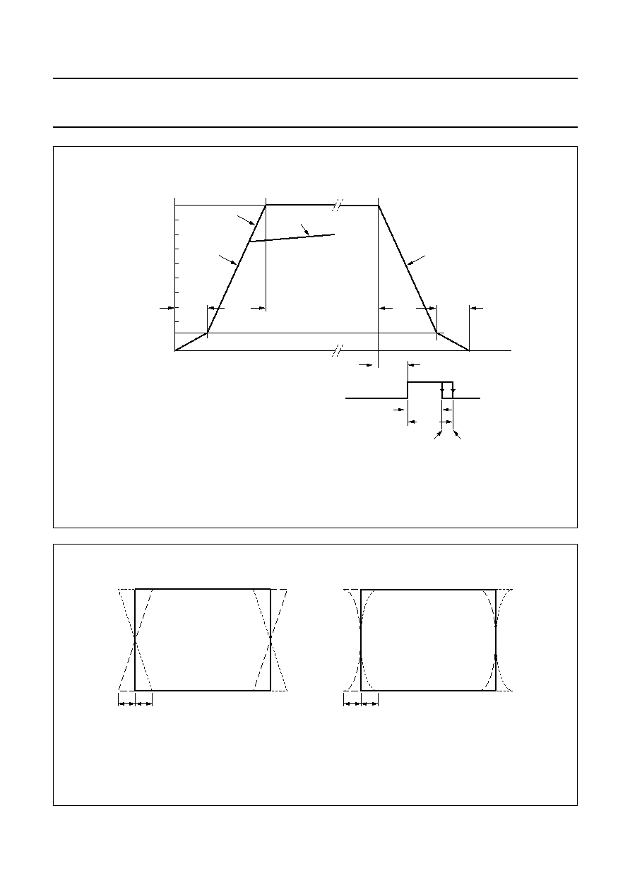
2002 Jun 04
43
Philips Semiconductors
Preliminary specification
I
2
C-bus controlled TV display processors
TDA933xH series
handbook, full pagewidth
MGS898
100
50
12
slow start
t (ms)
Ton
(% of nominal value)
32 ms
(1000 lines)
18 ms
57 ms
102 ms
slow stop
normal
ESS = 1
16 ms
25 ms
TFBC = 0
TFBC = 1
discharge
18.6 ms
Fig.15 Slow start behaviour of horizontal output, and slow stop behaviour and timing of picture tube discharge
pulse when IC is switched to standby via I
2
C-bus.
handbook, full pagewidth
MGS899
0.5
µ
s
0.5
µ
s
0.5
µ
s
0.5
µ
s
(a) Parallelogram correction.
(b) Bow correction.
Fig.16 Horizontal parallelogram and bow correction (figures for 1f
H
mode).
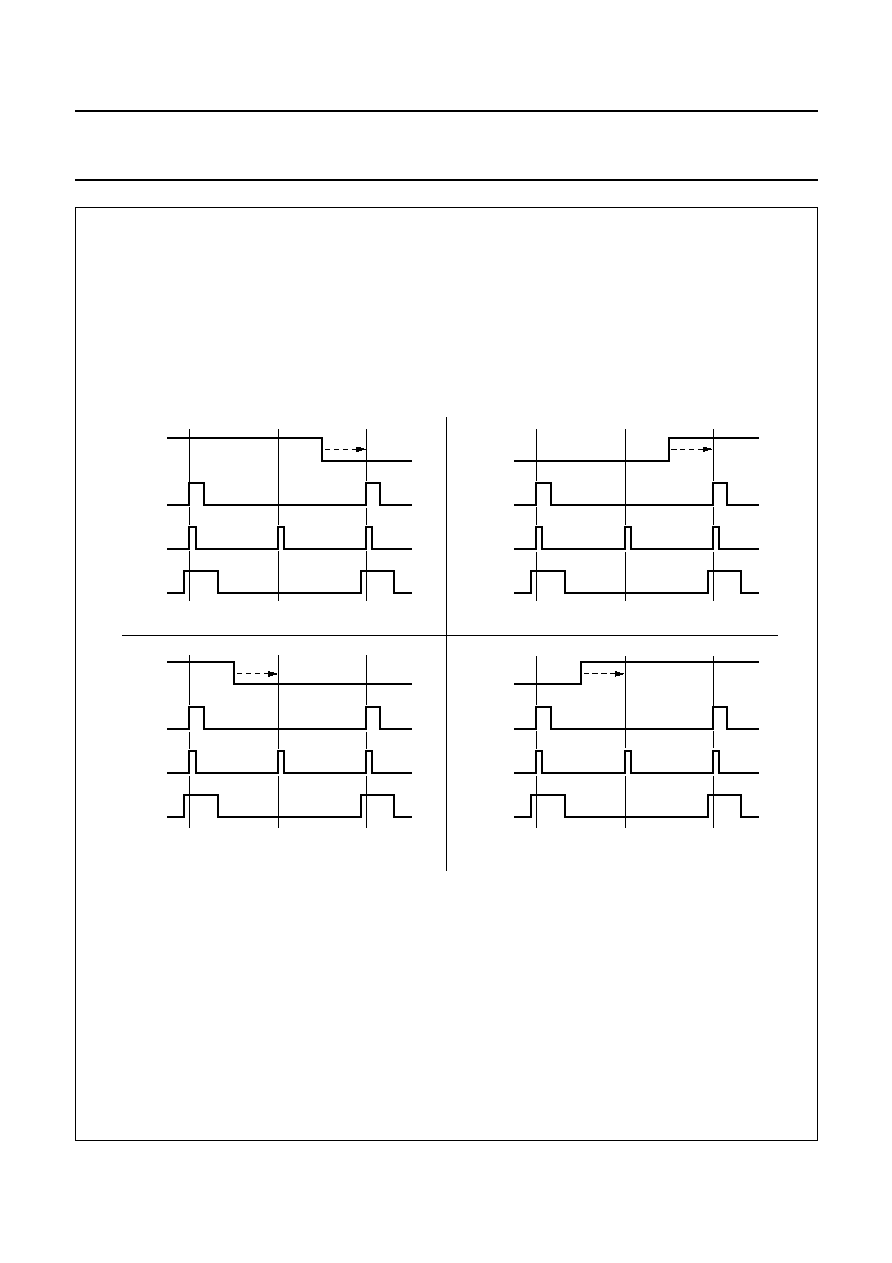
2002 Jun 04
44
Philips Semiconductors
Preliminary specification
I
2
C-bus controlled TV display processors
TDA933xH series
handbook, full pagewidth
MGS900
VD
HD
HBLNK
field 1 detection
VD
HD
HBLNK
field 2 detection
VD
HD
CLK2H
CLK2H
CLK2H
CLK2H
HBLNK
field 1 detection
VD
HD
HBLNK
field 2 detection
(a) End of VD pulse is reference (VSR = 0)
(b) Start of VD pulse is reference (VSR = 1)
Fig.17 Field detection mechanism.
See also Chapter "Characteristics"; note 41.

2002 Jun 04
45
Philips Semiconductors
Preliminary specification
I
2
C-bus controlled TV display processors
TDA933xH series
TEST AND APPLICATION INFORMATION
handbook, full pagewidth
MGR462
TDA932xH
FEATURE
BOX
TDA933xH
RO
YIN
Y
RGB-1
RGB-2
RGB-3
RGB-4
GO
UIN
U
BO
VDOA
VDOB
EWO
BCL
BLKIN
HFB
VIN
V
HOUT
HD
VD
HA
VA
IF
CVBS-1
TUNER AGC
AV-1
CVBS-2
CVBS
CVBS(PIP)
CVBS(TXT)
Y
C
CVBS/Y-3
C-3
CVBS/Y-4
C-4
AV-2
SAW
FILTER
COMB FILTER
Fig.18 Application diagram.

2002 Jun 04
46
Philips Semiconductors
Preliminary specification
I
2
C-bus controlled TV display processors
TDA933xH series
handbook, halfpage
600
400
200
0
-
200
-
400
-
600
0
t
time
0.5 t
(3)
(2)
(1)
MGL483
Ivert
(
µ
A)
Fig.19 Control range of vertical amplitude.
VSH = 31; SC = 0; I
VERT
= I
2(VDOB)
-
I
1(VDOA)
.
(1) VA = 0.
(2) VA = 31.
(3) VA = 63.
handbook, halfpage
0
Ivert
(
µ
A)
t
800
400
-
400
-
800
0
time
MGL484
0.5 t
(3)
(2)
(1)
Fig.20 Control range of vertical slope.
VA = 31; VHS = 31; SC = 0.
(1) VS = 0.
(2) VS = 31.
(3) VS = 63.
handbook, halfpage
600
400
200
0
-
200
-
400
-
600
0
t
time
MGL485
Ivert
(
µ
A)
0.5 t
(1)
(2)
(3)
VA = 31; SC = 0.
(1) VSH = 0.
(2) VSH = 31.
(3) VSH = 63.
Fig.0 Control range of vertical shift.
handbook, halfpage
600
400
200
0
-
200
-
400
-
600
0
t
time
MGL486
Ivert
(
µ
A)
0.5 t
(3)
(2)
(1)
Fig.22 Control range of S-correction.
VA = 31; VHS = 31.
(1) SC = 0.
(2) SC = 31.
(3) SC = 63.
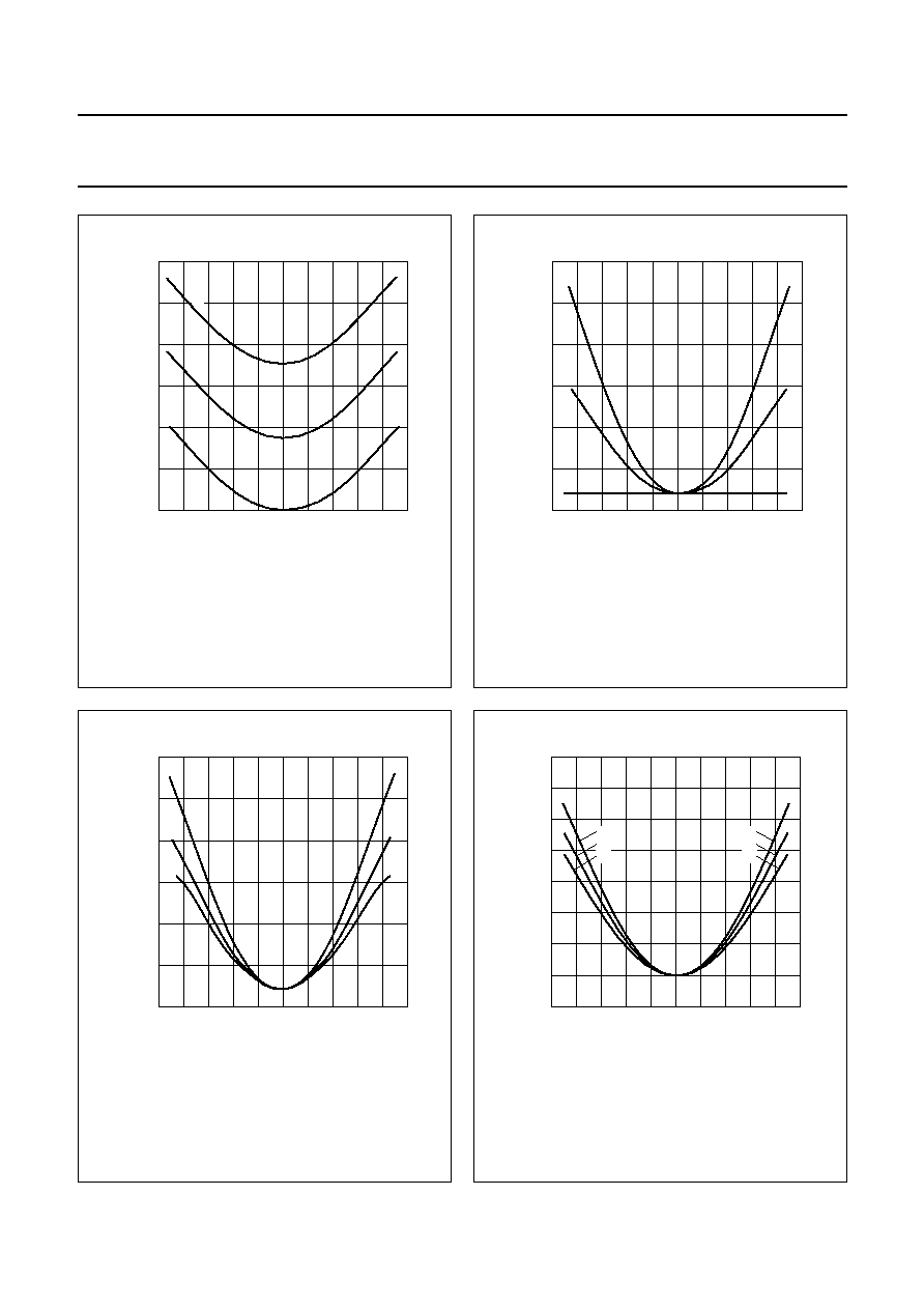
2002 Jun 04
47
Philips Semiconductors
Preliminary specification
I
2
C-bus controlled TV display processors
TDA933xH series
handbook, halfpage
0
200
t
time
800
400
1000
600
1200
0
MGL489
IEW
(
µ
A)
0.5 t
(3)
(2)
(1)
Fig.23 Control range of E-W width.
PW = 31; CP = 31.
(1) EW = 0.
(2) EW = 31.
(3) EW = 63.
handbook, halfpage
0
t
time
800
300
600
400
700
500
900
MGL488
IEW
(
µ
A)
0.5 t
(1)
(2)
(3)
EW = 31; CP = 31.
(1) PW = 0.
(2) PW = 31.
(3) PW = 63.
Fig.0 Control range of E-W parabola/width ratio.
handbook, halfpage
0
t
time
800
300
600
400
700
500
900
MGL487
IEW
(
µ
A)
0.5 t
(1)
(2)
(3)
Fig.25 Control range of E-W corner/parabola ratio.
EW = 31; PW = 63.
(1) CP = 0.
(2) CP = 31.
(3) CP = 63.
handbook, halfpage
0
t
time
200
800
400
1000
600
MGL490
IEW
(
µ
A)
0.5 t
(1)
(2)
(3)
(3)
(2)
(1)
Fig.26 Control range of E-W trapezium correction.
EW = 31; PW = 31.
(1) TC = 0.
(2) TC = 31.
(3) TC = 63.

2002 Jun 04
48
Philips Semiconductors
Preliminary specification
I
2
C-bus controlled TV display processors
TDA933xH series
Adjustment of geometry control parameters
The deflection processor of the TDA933xH offers
15 control parameters for picture alignment, as follows:
For the vertical picture alignment;
∑
S-correction
∑
Vertical amplitude
∑
Vertical slope
∑
Vertical shift
∑
Vertical zoom
∑
Vertical scroll
∑
Vertical wait.
For the horizontal picture alignment;
∑
Horizontal shift
∑
Horizontal parallelogram
∑
Horizontal bow
∑
E-W width with extended range for the zoom function
∑
E-W parabola/width ratio
∑
E-W upper corner/parabola ratio
∑
E-W lower corner/parabola ratio
∑
E-W trapezium correction.
It is important to notice that the ICs are designed for use
with a DC-coupled vertical deflection stage. This is why
a vertical linearity alignment is not necessary (and
therefore not available).
For a particular combination of picture tube type, vertical
output stage and E-W output stage, the required values for
the settings of S-correction and E-W corner/parabola ratio
must be determined. These parameters can be preset via
the I
2
C-bus and do not need any additional adjustment.
The rest of the parameters are preset with the mid-value of
their control range, i.e. 1FH, or with the values obtained by
previously-adjusted TV sets on the production line.
The vertical shift control is intended to compensate offsets
in the external vertical output stage or in the picture tube.
It can be shown that, without compensation, these offsets
will result in a certain linearity error, especially with picture
tubes that need large S-correction. In 1st-order
approximation, the total linearity error is proportional to the
value of the offset and to the square of the S-correction
that is needed. The necessity to use the vertical shift
alignment depends on the expected offsets in the vertical
output stage and picture tube, on the required value of the
S-correction and on the demands upon vertical linearity.
To adjust the vertical shift and vertical slope independently
of each other, a special service blanking mode can be
entered by setting bit SBL HIGH. In this mode, the RGB
outputs are blanked during the second half of the picture.
There are two different methods for alignment of the
picture in the vertical direction. Both methods use the
service blanking mode.
The first method is recommended for picture tubes that
have a marking for the middle of the screen. With the
vertical shift control, the last line of the visible picture is
positioned exactly in the middle of the screen. After this
adjustment, the vertical shift should not be changed any
more. The top of the picture is positioned by adjusting the
vertical amplitude, and the bottom by adjusting the vertical
slope.
The second method is recommended for picture tubes that
have no marking for the middle of the screen. For this
method, a video signal is required in which the middle of
the picture is indicated (e.g. the white line in the circle test
pattern). The beginning of the blanking is positioned
exactly on the middle of the picture using the vertical slope
control. The top and bottom of the picture are then
positioned symmetrically with respect to the middle of the
screen by adjusting the vertical amplitude and vertical
shift. After this adjustment, the vertical shift has the correct
setting and should not be changed any more.
If the vertical shift alignment is not required, VSH should
be set to its mid-value, i.e. VSH = 1FH (31 DEC). The top
of the picture is then positioned by adjusting the vertical
amplitude and the bottom of the picture by adjusting the
vertical slope.
After the vertical picture alignment, the picture is
positioned in the horizontal direction by adjusting the E-W
width, E-W parabola/width ratio and horizontal shift. Finally
(if necessary), the left and right-hand sides of the picture
are aligned in parallel by adjusting the E-W trapezium
control.
Additional horizontal corrections are possible using the
parallelogram and bow controls.
To obtain the correct range of the vertical zoom function,
the vertical geometry should be adjusted at a nominal
setting of the zoom DAC at position 19H (25 DEC) and the
vertical scroll DAC at 1FH (31 DEC).

2002 Jun 04
49
Philips Semiconductors
Preliminary specification
I
2
C-bus controlled TV display processors
TDA933xH series
PACKAGE OUTLINE
UNIT
A
1
A
2
A
3
b
p
c
E
(1)
e
H
E
L
L
p
Z
y
w
v
REFERENCES
OUTLINE
VERSION
EUROPEAN
PROJECTION
ISSUE DATE
IEC
JEDEC
EIAJ
mm
0.25
0.05
1.85
1.65
0.25
0.40
0.20
0.25
0.14
10.1
9.9
0.8
1.3
12.9
12.3
1.2
0.8
10
0
o
o
0.15
0.1
0.15
DIMENSIONS (mm are the original dimensions)
Note
1. Plastic or metal protrusions of 0.25 mm maximum per side are not included.
0.95
0.55
SOT307-2
95-02-04
97-08-01
D
(1)
(1)
(1)
10.1
9.9
H
D
12.9
12.3
E
Z
1.2
0.8
D
e
E
B
11
c
E
H
D
ZD
A
Z E
e
v
M
A
X
1
44
34
33
23
22
12
y
A
1
A
L
p
detail X
L
(A )
3
A
2
pin 1 index
D
H
v
M
B
b
p
b
p
w
M
w
M
0
2.5
5 mm
scale
QFP44: plastic quad flat package; 44 leads (lead length 1.3 mm); body 10 x 10 x 1.75 mm
SOT307-2
A
max.
2.10

2002 Jun 04
50
Philips Semiconductors
Preliminary specification
I
2
C-bus controlled TV display processors
TDA933xH series
SOLDERING
Introduction to soldering surface mount packages
This text gives a very brief insight to a complex technology.
A more in-depth account of soldering ICs can be found in
our
"Data Handbook IC26; Integrated Circuit Packages"
(document order number 9398 652 90011).
There is no soldering method that is ideal for all surface
mount IC packages. Wave soldering is not always suitable
for surface mount ICs, or for printed-circuit boards with
high population densities. In these situations reflow
soldering is often used.
Reflow soldering
Reflow soldering requires solder paste (a suspension of
fine solder particles, flux and binding agent) to be applied
to the printed-circuit board by screen printing, stencilling or
pressure-syringe dispensing before package placement.
Several methods exist for reflowing; for example,
infrared/convection heating in a conveyor type oven.
Throughput times (preheating, soldering and cooling) vary
between 100 and 200 seconds depending on heating
method.
Typical reflow peak temperatures range from
215 to 250
∞
C. The top-surface temperature of the
packages should preferable be kept below 230
∞
C.
Wave soldering
Conventional single wave soldering is not recommended
for surface mount devices (SMDs) or printed-circuit boards
with a high component density, as solder bridging and
non-wetting can present major problems.
To overcome these problems the double-wave soldering
method was specifically developed.
If wave soldering is used the following conditions must be
observed for optimal results:
∑
Use a double-wave soldering method comprising a
turbulent wave with high upward pressure followed by a
smooth laminar wave.
∑
For packages with leads on two sides and a pitch (e):
≠ larger than or equal to 1.27 mm, the footprint
longitudinal axis is preferred to be parallel to the
transport direction of the printed-circuit board;
≠ smaller than 1.27 mm, the footprint longitudinal axis
must be parallel to the transport direction of the
printed-circuit board.
The footprint must incorporate solder thieves at the
downstream end.
∑
For packages with leads on four sides, the footprint must
be placed at a 45
∞
angle to the transport direction of the
printed-circuit board. The footprint must incorporate
solder thieves downstream and at the side corners.
During placement and before soldering, the package must
be fixed with a droplet of adhesive. The adhesive can be
applied by screen printing, pin transfer or syringe
dispensing. The package can be soldered after the
adhesive is cured.
Typical dwell time is 4 seconds at 250
∞
C.
A mildly-activated flux will eliminate the need for removal
of corrosive residues in most applications.
Manual soldering
Fix the component by first soldering two
diagonally-opposite end leads. Use a low voltage (24 V or
less) soldering iron applied to the flat part of the lead.
Contact time must be limited to 10 seconds at up to
300
∞
C.
When using a dedicated tool, all other leads can be
soldered in one operation within 2 to 5 seconds between
270 and 320
∞
C.

2002 Jun 04
51
Philips Semiconductors
Preliminary specification
I
2
C-bus controlled TV display processors
TDA933xH series
Suitability of surface mount IC packages for wave and reflow soldering methods
Notes
1. All surface mount (SMD) packages are moisture sensitive. Depending upon the moisture content, the maximum
temperature (with respect to time) and body size of the package, there is a risk that internal or external package
cracks may occur due to vaporization of the moisture in them (the so called popcorn effect). For details, refer to the
Drypack information in the
"Data Handbook IC26; Integrated Circuit Packages; Section: Packing Methods".
2. These packages are not suitable for wave soldering as a solder joint between the printed-circuit board and heatsink
(at bottom version) can not be achieved, and as solder may stick to the heatsink (on top version).
3. If wave soldering is considered, then the package must be placed at a 45
∞
angle to the solder wave direction.
The package footprint must incorporate solder thieves downstream and at the side corners.
4. Wave soldering is only suitable for LQFP, TQFP and QFP packages with a pitch (e) equal to or larger than 0.8 mm;
it is definitely not suitable for packages with a pitch (e) equal to or smaller than 0.65 mm.
5. Wave soldering is only suitable for SSOP and TSSOP packages with a pitch (e) equal to or larger than 0.65 mm; it is
definitely not suitable for packages with a pitch (e) equal to or smaller than 0.5 mm.
DATA SHEET STATUS
Notes
1. Please consult the most recently issued data sheet before initiating or completing a design.
2. The product status of the device(s) described in this data sheet may have changed since this data sheet was
published. The latest information is available on the Internet at URL http://www.semiconductors.philips.com.
PACKAGE
SOLDERING METHOD
WAVE
REFLOW
(1)
BGA, LFBGA, SQFP, TFBGA
not suitable
suitable
HBCC, HLQFP, HSQFP, HSOP, HTQFP, HTSSOP, SMS
not suitable
(2)
suitable
PLCC
(3)
, SO, SOJ
suitable
suitable
LQFP, QFP, TQFP
not recommended
(3)(4)
suitable
SSOP, TSSOP, VSO
not recommended
(5)
suitable
DATA SHEET STATUS
(1)
PRODUCT
STATUS
(2)
DEFINITIONS
Objective data
Development
This data sheet contains data from the objective specification for product
development. Philips Semiconductors reserves the right to change the
specification in any manner without notice.
Preliminary data
Qualification
This data sheet contains data from the preliminary specification.
Supplementary data will be published at a later date. Philips
Semiconductors reserves the right to change the specification without
notice, in order to improve the design and supply the best possible
product.
Product data
Production
This data sheet contains data from the product specification. Philips
Semiconductors reserves the right to make changes at any time in order
to improve the design, manufacturing and supply. Changes will be
communicated according to the Customer Product/Process Change
Notification (CPCN) procedure SNW-SQ-650A.

2002 Jun 04
52
Philips Semiconductors
Preliminary specification
I
2
C-bus controlled TV display processors
TDA933xH series
DEFINITIONS
Short-form specification
The data in a short-form
specification is extracted from a full data sheet with the
same type number and title. For detailed information see
the relevant data sheet or data handbook.
Limiting values definition
Limiting values given are in
accordance with the Absolute Maximum Rating System
(IEC 60134). Stress above one or more of the limiting
values may cause permanent damage to the device.
These are stress ratings only and operation of the device
at these or at any other conditions above those given in the
Characteristics sections of the specification is not implied.
Exposure to limiting values for extended periods may
affect device reliability.
Application information
Applications that are
described herein for any of these products are for
illustrative purposes only. Philips Semiconductors make
no representation or warranty that such applications will be
suitable for the specified use without further testing or
modification.
DISCLAIMERS
Life support applications
These products are not
designed for use in life support appliances, devices, or
systems where malfunction of these products can
reasonably be expected to result in personal injury. Philips
Semiconductors customers using or selling these products
for use in such applications do so at their own risk and
agree to fully indemnify Philips Semiconductors for any
damages resulting from such application.
Right to make changes
Philips Semiconductors
reserves the right to make changes, without notice, in the
products, including circuits, standard cells, and/or
software, described or contained herein in order to
improve design and/or performance. Philips
Semiconductors assumes no responsibility or liability for
the use of any of these products, conveys no licence or title
under any patent, copyright, or mask work right to these
products, and makes no representations or warranties that
these products are free from patent, copyright, or mask
work right infringement, unless otherwise specified.
PURCHASE OF PHILIPS I
2
C COMPONENTS
Purchase of Philips I
2
C components conveys a license under the Philips' I
2
C patent to use the
components in the I
2
C system provided the system conforms to the I
2
C specification defined by
Philips. This specification can be ordered using the code 9398 393 40011.

2002 Jun 04
53
Philips Semiconductors
Preliminary specification
I
2
C-bus controlled TV display processors
TDA933xH series
NOTES

2002 Jun 04
54
Philips Semiconductors
Preliminary specification
I
2
C-bus controlled TV display processors
TDA933xH series
NOTES

2002 Jun 04
55
Philips Semiconductors
Preliminary specification
I
2
C-bus controlled TV display processors
TDA933xH series
NOTES

© Koninklijke Philips Electronics N.V. 2002
SCA74
All rights are reserved. Reproduction in whole or in part is prohibited without the prior written consent of the copyright owner.
The information presented in this document does not form part of any quotation or contract, is believed to be accurate and reliable and may be changed
without notice. No liability will be accepted by the publisher for any consequence of its use. Publication thereof does not convey nor imply any license
under patent- or other industrial or intellectual property rights.
Philips Semiconductors ≠ a worldwide company
Contact information
For additional information please visit http://www.semiconductors.philips.com.
Fax: +31 40 27 24825
For sales offices addresses send e-mail to: sales.addresses@www.semiconductors.philips.com.
Printed in The Netherlands
753504/03/pp
56
Date of release:
2002 Jun 04
Document order number:
9397 750 09383