 | –≠–ª–µ–∫—Ç—Ä–æ–Ω–Ω—ã–π –∫–æ–º–ø–æ–Ω–µ–Ω—Ç: TDA958X | –°–∫–∞—á–∞—Ç—å:  PDF PDF  ZIP ZIP |

DATA SHEET
Tentative Device Specification
File under Integrated Circuits, <Handbook>
2000 Jun 22
INTEGRATED CIRCUITS
TDA955X/6X/8X PS/N1 series
TV signal processor-Teletext
decoder with embedded
µ
-Controller
DEVICE SPECIFICATION
Previous date: 2000 Apr 06
Version: 1.6

2000 Jun 22
2
Philips Semiconductors
Tentative Device Specification
TV signal processor-Teletext decoder
with embedded
µ
-Controller
TDA955X/6X/8X PS/N1 series
GENERAL DESCRIPTION
The various versions of the TDA955X/6X/8X PS/N1 series
combine the functions of a video processor together with a
µ
-Controller and US Closed Caption decoder. Several
versions have a Teletext decoder on board. The Teletext
decoder has an internal RAM memory for 1or 10 page text.
The ICs are intended to be used in economy television
receivers with 90
∞
and 110
∞
picture tubes.
The ICs have supply voltages of 8 V and 3.3 V and they
are mounted in an S-DIP 64 envelope.
The features are given in the following feature list. The
differences between the various ICs are given in the table
on page 4.
FEATURES
TV-signal processor
∑
Multi-standard vision IF circuit with alignment-free PLL
demodulator
∑
Internal (switchable) time-constant for the IF-AGC circuit
∑
A choice can be made between versions with mono
intercarrier sound FM demodulator and versions with
QSS IF amplifier. In the QSS versions without
East-West output an AM/FM mode can be activated. In
that case both the QSS amplifier (for AM demodulation)
and the FM demodulator are available.
∑
The mono intercarrier sound circuit has a selective
FM-PLL demodulator which can be switched to the
different FM sound frequencies (4.5/5.5/6.0/6.5 MHz).
The quality of this system is such that the external
band-pass filters can be omitted.
∑
The FM-PLL demodulator can be set to centre
frequencies of 4.74/5.74 MHz so that a second sound
channel can be demodulated. In such an application it is
necessary that an external bandpass filter is inserted.
∑
The QSS amplifier and mono intercarrier sound circuit of
some versions can be used for the demodulation of FM
radio signals
∑
Source selection between the `internal' CVBS and one
external CVBS or Y/C signal
∑
Integrated chrominance trap circuit
∑
Integrated luminance delay line with adjustable delay
time
∑
Picture improvement features with peaking (with
switchable centre frequency, depeaking, variable
positive/negative overshoot ratio and video dependent
coring) and blue- and black stretching
∑
Integrated chroma band-pass filter with switchable
centre frequency
∑
Only one reference (12 MHz) crystal required for the
µ
-Controller, Teletext- and the colour decoder
∑
PAL/NTSC or multi-standard colour decoder with
automatic search system
∑
Internal base-band delay line
∑
Indication of the Signal-to-Noise ratio of the incoming
CVBS signal
∑
RGB control circuit with `Continuous Cathode
Calibration', white point and black level off-set
adjustment so that the colour temperature of the dark
and the light parts of the screen can be chosen
independently.
∑
A linear RGB/YUV/YP
B
P
R
input with fast blanking for
external RGB/YUV sources. The synchronisation circuit
can be connected to the incoming Y signal. The
Text/OSD signals are internally supplied from the
µ
-Controller/Teletext decoder.
∑
Contrast reduction possibility during mixed-mode of
OSD and Text signals
∑
Adjustable `wide blanking' of the RGB outputs
∑
Horizontal synchronization with two control loops and
alignment-free horizontal oscillator
∑
Vertical count-down circuit
∑
Vertical driver optimized for DC-coupled vertical output
stages
∑
Horizontal and vertical geometry processing
∑
Horizontal and vertical zoom function for 16 : 9
applications
∑
Horizontal parallelogram and bow correction for large
screen picture tubes
∑
Low-power start-up of the horizontal drive circuit

2000 Jun 22
3
Philips Semiconductors
Tentative Device Specification
TV signal processor-Teletext decoder with
embedded
µ
-Controller
TDA955X/6X/8X PS/N1 series
µ
-Controller
∑
80C51
µ
-controller core standard instruction set and
timing
∑
1
µ
s machine cycle
∑
32 - 128Kx8-bit late programmed ROM
∑
3 - 12Kx8-bit Auxiliary RAM (shared with Display and
Acquisition)
∑
Interrupt controller for individual enable/disable with two
level priority
∑
Two 16-bit Timer/Counter registers
∑
One 16 bit Timer with 8-bit Pre-scaler
∑
WatchDog timer
∑
Auxiliary RAM page pointer
∑
16-bit Data pointer
∑
Stand-by, Idle and Power Down (PD) mode
∑
14 bits PWM for Voltage Synthesis Tuning
∑
8-bit A/D converter
∑
4 pins which can be programmed as general I/O pin,
ADC input or PWM (6-bit) output
Data Capture
∑
Text memory for 0, 1 or 10 pages
∑
In the 10 page versions inventory of transmitted Teletext
pages stored in the Transmitted Page Table (TPT) and
Subtitle Page Table (SPT)
∑
Data Capture for US Closed Caption
∑
Data Capture for 525/625 line WST, VPS (PDC system
A) and Wide Screen Signalling (WSS) bit decoding
∑
Automatic selection between 525 WST/625 WST
∑
Automatic selection between 625 WST/VPS on line 16
of VBI
∑
Real-time capture and decoding for WST Teletext in
Hardware, to enable optimized
µ
-processor throughput
∑
Automatic detection of FASTEXT transmission
∑
Real-time packet 26 engine in Hardware for processing
accented, G2 and G3 characters
∑
Signal quality detector for video and WST/VPS data
types
∑
Comprehensive teletext language coverage
∑
Full Field and Vertical Blanking Interval (VBI) data
capture of WST data
Display
∑
Teletext and Enhanced OSD modes
∑
Features of level 1.5 WST and US Close Caption
∑
Serial and Parallel Display Attributes
∑
Single/Double/Quadruple Width and Height for
characters
∑
Scrolling of display region
∑
Variable flash rate controlled by software
∑
Enhanced display features including overlining,
underlining and italics
∑
Soft colours using CLUT with 4096 colour palette
∑
Globally selectable scan lines per row (9/10/13/16) and
character matrix [12x10, 12x13, 12x16 (VxH)]
∑
Fringing (Shadow) selectable from N-S-E-W direction
∑
Fringe colour selectable
∑
Meshing of defined area
∑
Contrast reduction of defined area
∑
Cursor
∑
Special Graphics Characters with two planes, allowing
four colours per character
∑
32 software redefinable On-Screen display characters
∑
4 WST Character sets (G0/G2) in single device (e.g.
Latin, Cyrillic, Greek, Arabic)
∑
G1 Mosaic graphics, Limited G3 Line drawing
characters
∑
WST Character sets and Closed Caption Character set
in single device

2000 Jun 22
4
Philips Semiconductors
T
entativ
e De
vice Specification
TV signal processor-T
elete
xt decoder with
embedded
µ
-Controller
TD
A955X/6X/8X PS/N1 ser
ies
FUNCTIONAL DIFFERENCE BETWEEN THE VARIOUS IC VERSIONS
IC VERSION (TDA95XX PS)
50
51
52
53
54
60
61
62
63
64
65
66
67
80
81
82
83
84
85
86
87
88
TV range
90
∞
90
∞
90
∞
110
∞
90
∞
90
∞
90
∞
110
∞
110
∞
110
∞
110
∞
90
∞
90
∞
90
∞
90
∞
90
∞
110
∞
110
∞
110
∞
110
∞
90
∞
110
∞
Mono intercarrier multi-standard
sound demodulator (4.5 - 6.5 MHz)
with switchable centre frequency
Audio switch
Automatic Volume Levelling
Automatic Volume Levelling or
subcarrier output (for comb filter
applications)
QSS sound IF amplifier with
separate input and AGC circuit
AM sound demodulator without
extra reference circuit
AM/FM option
FM radio option (via QSS amplifier)
FM radio option (with FM tuner)
Dynamic Skin tone control
PAL decoder
SECAM decoder
NTSC decoder
Horizontal geometry (E-W)
Horizontal and Vertical Zoom
ROM size
32 -
64 k
32 -
64 k
32 -
64 k
32 -
64 k
32 -
64 k
64-
128k
64-
128k
64 -
128k
64 -
128k
64 -
128k
64 -
128k
64 -
128k
64 -
128k
64 k 64 k 64 k 64 k 64 k 64 k 64 k 64 k 64 k
User RAM size
1 k
1 k
1 k
1 k
1 k
2 k
2 k
2 k
2 k
2 k
2 k
2 k
2 k
1 k
1 k
1 k
1 k
1 k
1 k
1 k
1 k
1 k
Teletext
1
page
1
page
1
page
1
page
1
page
10
page
10
page
10
page
10
page
10
page
10
page
10
page
10
page
Closed captioning

2000 Jun 22
5
Philips Semiconductors
Tentative Device Specification
TV signal processor-Teletext decoder with
embedded
µ
-Controller
TDA955X/6X/8X PS/N1 series
QUICK REFERENCE DATA
SYMBOL
PARAMETER
MIN.
TYP.
MAX.
UNIT
Supply
V
P
supply voltages
-
8.0/3.3
-
V
I
P
supply current
-
tbf
-
mA
Input voltages
V
iVIFrms)
video IF amplifier sensitivity (RMS value)
-
35
-
µ
V
V
iSIF(rms)
QSS sound IF amplifier sensitivity (RMS value)
-
60
-
µ
V
V
iAUDIO(rms)
external audio input (RMS value)
-
500
-
mV
V
iCVBS(p-p)
external CVBS/Y input (peak-to-peak value)
-
1.0
-
V
V
iCHROMA(p-p)
external chroma input voltage (burst amplitude)
(peak-to-peak value)
-
0.3
-
V
V
iRGB(p-p)
RGB inputs (peak-to-peak value)
-
0.7
-
V
V
iY(p-p)
luminance input signal (peak-to-peak value)
-
1.4 / 1.0
-
V
V
iU(p-p)
/
V
iPB(p-p)
U / P
B
input signal (peak-to-peak value)
-
-
1.33 /
+0.7
-
V
V
iV(p-p) /
V
iPR(p-p)
V / P
R
input signal (peak-to-peak value)
-
-
1.05 /
+0.7
-
V
Output signals
V
o(IFVO)(p-p)
demodulated CVBS output (peak-to-peak value)
-
2.0
-
V
V
o(QSSO)(rms)
sound IF intercarrier output in QSS versions (RMS value)
-
100
-
mV
V
o(AMOUT)(rms)
demodulated AM sound output in QSS versions (RMS
value)
-
500
-
mV
V
o(CVBSO)(p-p)
selected CVBS output (peak-to-peak value)
-
2.0
-
V
I
o(AGCOUT)
tuner AGC output current range
0
-
5
mA
V
oRGB(p-p)
RGB output signal amplitudes (peak-to-peak value)
-
2.0
-
V
I
oHOUT
horizontal output current
10
-
-
mA
I
oVERT
vertical output current (peak-to-peak value)
1
-
-
mA
I
oEWD
EW drive output current
1.2
-
-
mA

2000 Jun 22
6
Philips Semiconductors
Tentative Device Specification
TV signal processor-Teletext decoder with
embedded
µ
-Controller
TDA955X/6X/8X PS/N1 series
BLOCK DIAGRAM
SOUND
TRAP
TUNERA
GC
+8V
HOUT
V
-DRIVE
RO
GO
B0
BCLIN
BLKIN
CVBS/Y
IFIN
AUDOUT
AUDEXT
Fig. 1 Block diagram TDA955X/6X/8X PS/N1 series with mono intercarrier sound demodulator
C
SD
A
SCL
VISION IF
ALIGNMENT-FREE
PLL DEMOD.
AGC/AFC
VIDEO AMP.
VIDEO SWITCH
VIDEO IDENT.
VIDEO FILTERS
PAL/SECAM/NTSC
DECODER
DEEMPHASIS
AUDIO SWITCH
(AVL)
VOLUME CONTROL
BASE-BAND
DELAY LINE
H/V SYNC SEP.
H-OSC. + PLL
H-DRIVE
2
nd
LOOP
H-SHIFT
V-DRIVE +
CONTR/BRIGHTN
OSD/TEXT INSERT
CCC
WHITE-P. ADJ.
80C51 CPU
I
2
C-BUS
TRANSCEIVER
ROM/RAM
TELETEXT
ACQUISITION
1/10 PAGE
MEMORY
TELETEXT/OSD
DISPLAY
RG
B
BL
Y
U
V
H
V
REF
ENHANCED
VST PWM-DAC
VST OUT
I/O PORTS
I/O PORTS (4x)
+3.3 V
RESET
LED OUT (2x)
ADC IN (4x)
VPE
(EW GEOMETRY)
GEOMETRY
EHTO
(EWD)
R/V
G/Y
B/U
BL
RGB/YUV INSERT
R
GB
REF
CVBS
SYNC
H
V
COR
RGB/YUV MATRIX
SATURATION
YUV/RGB MATRIX
LUMA DELAY
PEAKING
BLACK STRETCH
AGC CIRCUIT
NARROW BAND
PLL
DEMODULATOR
(AVL)
DEEMPHASIS
(REFOUT)

2000 Jun 22
7
Philips Semiconductors
Tentative Device Specification
TV signal processor-Teletext decoder with
embedded
µ
-Controller
TDA955X/6X/8X PS/N1 series
SOUND
TRAP
TUNERA
GC
+8V
HOUT
V
-DRIVE
RO
GO
BO
BCLIN
BLKIN
CVBS/Y
IFIN
Fig. 2 Block diagram TDA955X/6X/8X PS/N1 series with QSS IF sound channel
C
SD
A
SCL
VISION IF
ALIGNMENT-FREE
PLL DEMOD.
AGC/AFC
VIDEO AMP.
VIDEO SWITCH
VIDEO IDENT.
VIDEO FILTERS
PAL/SECAM/NTSC
DECODER
LUMA DELAY
PEAKING
BLACK STRETCH
BASE-BAND
DELAY LINE
H/V SYNC SEP.
H-OSC. + PLL
H-DRIVE
2
nd
LOOP
H-SHIFT
V-DRIVE +
CONTR/BRIGHTN
OSD/TEXT INSERT
CCC
WHITE-P. ADJ.
80C51 CPU
I
2
C-BUS
TRANSCEIVER
ROM/RAM
TELETEXT
ACQUISITION
10 PAGE
MEMORY
TELETEXT/OSD
DISPLAY
RG
B
BL
Y
U
V
H
V
REF
ENHANCED
VST PWM-DAC
VST OUT
I/O PORTS
I/O PORTS (4x)
+3.3 V
RESET
LED OUT (2x)
ADC IN (4x)
VPE
EW GEOMETRY
GEOMETRY
EHTO
EWD
R/V
G/Y
B/U
BL
RGB/YUV INSERT
R
GB
REF
CVBS
SYNC
H
V
COR
RGB/YUV MATRIX
SATURATION
YUV/RGB MATRIX
QSS SOUND IF
AGC
QSS MIXER
AM DEMODULTOR
SIFIN
QSSO/AMOUT/AUDEXT
AUDOUT/AMOUT
(REFOUT)

2000 Jun 22
8
Philips Semiconductors
Tentative Device Specification
TV signal processor-Teletext decoder with
embedded
µ
-Controller
TDA955X/6X/8X PS/N1 series
SOUND
TRAP
TUNERA
GC
+8V
HOUT
V
-DRIVE
RO
GO
BO
BCLIN
BLKIN
CVBS/Y
SIFIN
AUDOUT/AMOUT
Fig. 3 Block diagram TDA955X/6X/8X PS/N1 series with QSS IF in AM/FM mode
C
SD
A
SCL
VISION IF
ALIGNMENT-FREE
PLL DEMOD.
AGC/AFC
VIDEO AMP.
VIDEO SWITCH
VIDEO IDENT.
VIDEO FILTERS
PAL/SECAM/NTSC
DECODER
DEEMPHASIS
AUDIO SWITCH
(AVL)
VOLUME CONTROL
BASE-BAND
DELAY LINE
H/V SYNC SEP.
H-OSC. + PLL
H-DRIVE
2
nd
LOOP
H-SHIFT
V-DRIVE +
CONTR/BRIGHTN
OSD/TEXT INSERT
CCC
WHITE-P. ADJ.
80C51 CPU
I
2
C-BUS
TRANSCEIVER
ROM/RAM
TELETEXT
ACQUISITION
1/10 PAGE
MEMORY
TELETEXT/OSD
DISPLAY
RG
B
BL
Y
U
V
H
V
REF
ENHANCED
VST PWM-DAC
VST OUT
I/O PORTS
I/O PORTS (4x)
+3.3 V
RESET
LED OUT (2x)
ADC IN (4x)
VPE
GEOMETRY
EHTO
R/V
G/Y
B/U
BL
RGB/YUV INSERT
R
GB
REF
CVBS
SYNC
H
V
COR
SATURATION
LUMA DELAY
PEAKING
BLACK STRETCH
SIF SOUND IF
AGC
AM DEMODULATOR
SOUND PLL
VIFIN
WHITE STRETCH
BLUE STRETCH
AUDEXT
GROUP DELAY
CORRECTION
DEEMPHASIS

2000 Jun 22
9
Philips Semiconductors
Tentative Device Specification
TV signal processor-Teletext decoder with
embedded
µ
-Controller
TDA955X/6X/8X PS/N1 series
PINNING (GENERAL VERSION)
SYMBOL
PIN
DESCRIPTION
P1.3/T1
1
port 1.3 or Counter/Timer 1 input
P1.6/SCL
2
port 1.6 or I
2
C-bus clock line
P1.7/SDA
3
port 1.7 or I
2
C-bus data line
P2.0/TPWM
4
port 2.0 or Tuning PWM output
P3.0/ADC0
5
port 3.0 or ADC0 input
P3.1/ADC1
6
port 3.1 or ADC1 input
P3.2/ADC2
7
port 3.2 or ADC2 input
P3.3/ADC3
8
port 3.3 or ADC3 input
VSSC/P
9
digital ground for
µ
-Controller core and periphery
P0.5
10
port 0.5 (8 mA current sinking capability for direct drive of LEDs)
P0.6
11
port 0.6 (8 mA current sinking capability for direct drive of LEDs)
VSSA
12
analog ground of Teletext decoder and digital ground of TV-processor
SECPLL
13
SECAM PLL decoupling
VP2
14
2
nd
supply voltage TV-processor (+8V)
DECDIG
15
supply voltage of digital circuit of TV-processor
PH2LF
16
phase-2 filter
PH1LF
17
phase-1 filter
GND3
18
ground 3 for TV-processor
DECBG
19
bandgap decoupling
AVL/EWD
/DECSDEM
(1)
20
Automatic Volume Levelling (90
∞
versions) / E-W drive output (110
∞
versions) /
decoupling sound demodulator (QSS version in AM/FM mode)
VDRB
21
vertical drive B output
VDRA
22
vertical drive A output
IFIN1
23
IF input 1
IFIN2
24
IF input 2
IREF
25
reference current input
VSC
26
vertical sawtooth capacitor
AGCOUT
27
tuner AGC output
AUDEEM/SIFIN1
(1)
28
audio deemphasis or SIF input 1
DECSDEM/SIFIN2
(1)
29
decoupling sound demodulator or SIF input 2
GND2
30
ground 2 for TV processor
SNDPLL/SIFAGC/
(1)
31
narrow band PLL filter or AGC sound IF
AVL/SNDIF/REF0/
AMOUT/AUDEEM
(1)
32
Automatic Volume Levelling / sound IF input / subcarrier reference output / AM
output (non controlled) / audio deemphasis (QSS version in AM/FM mode)
HOUT
33
horizontal output
FBISO
34
flyback input/sandcastle output
AUDEXT/QSSO
/AMOUT
(1)
35
external audio output / QSS intercarrier out / AM audio output (non controlled)
EHTO
36
EHT/overvoltage protection input
PLLIF
37
IF-PLL loop filter
IFVO/SVO
38
IF video output / selected CVBS output
VP1
39
supply voltage TV processor

2000 Jun 22
10
Philips Semiconductors
Tentative Device Specification
TV signal processor-Teletext decoder with
embedded
µ
-Controller
TDA955X/6X/8X PS/N1 series
Note
1. The function of pin 20, 28, 29, 31, 32, 35 and 44 is dependent on the IC version (mono intercarrier FM demodulator
/ QSS IF amplifier and East-West output or not) and on some software control bits. The valid combinations are given
in table 1.
CVBS1
40
internal CVBS input
GND
41
ground for TV processor
CVBS/Y
42
CVBS/Y input
C
43
C input
AUDOUT /AMOUT
(1)
44
audio output /AM audio output (volume controlled)
INSSW2
45
2
nd
RGB / YUV insertion input
R2/VIN
46
2
nd
R input / V (R-Y) input / P
R
input
G2/YIN
47
2
nd
G input / Y input
B2/UIN
48
2
nd
B input / U (B-Y) input / P
B
input
BCLIN
49
beam current limiter input
BLKIN
50
black current input / V-guard input
RO
51
Red output
GO
52
Green output
BO
53
Blue output
VDDA
54
analog supply of Teletext decoder and digital supply of TV-processor (3.3 V)
VPE
55
OTP Programming Voltage
VDDC
56
digital supply to core (3.3 V)
OSCGND
57
oscillator ground supply
XTALIN
58
crystal oscillator input
XTALOUT
59
crystal oscillator output
RESET
60
reset
VDDP
61
digital supply to periphery (+3.3 V)
P1.0/INT1
62
port 1.0 or external interrupt 1 input
P1.1/T0
63
port 1.1 or Counter/Timer 0 input
P1.2/INT0
64
port 1.2 or external interrupt 0 input
SYMBOL
PIN
DESCRIPTION

2000 Jun 22
11
Philips Semiconductors
T
entativ
e De
vice Specification
TV signal processor-T
elete
xt decoder with
embedded
µ
-Controller
TD
A955X/6X/8X PS/N1 ser
ies
Table 1
Pin functions for various versions
Note
1. When the AM/FM mode is chosen several pins have a different function. For this reason this mode can be selected only when the adapted
application is used.
2. When in the AM/FM mode the AM bit is activated a capacitor with a value of about 2.2
µ
F has to be switched externally in parallel with the sound
PLL filter
3. When additional (external) selectivity is required for FM-PLL system pin 32 can be used as sound IF input. This function is selected by means of
SIF bit in subaddress 21H.
IC version
FM-PLL version
QSS VERSION
AM/FM MODE
(1)
NORMAL MODE
AMFM bit
0
1
0
East-West Y/N
N
Y
N
N
Y
CMB1/CMB0 bits
00
01/10/11
00
01/10/11
-
00
01/10/11
00
01/10/11
AM bit
-
-
-
-
0
1
-
0
1
-
0
1
Pin 20
AVL
EWD
DECSDEM
AVL
EWD
Pin 28
AUDEEM
SIFIN1
SIFIN1
Pin 29
DECSDEM
SIFIN2
SIFIN2
Pin 31
SNDPLL
SNDPLL SIFAGC
(2)
SIFAGC
Pin 32
SNDIF
(3)
REFO AVL/SNDIF
(3)
REFO
AUDEEM/AMOUT
AMOUT
REFO
AMOUT
REFO
Pin 35
AUDEXT
AUDEXT
AUDEXT
QSSO
AMOUT
AUDEXT
QSSO
AMOUT
Pin 44
AUDOUT
controlled audio out
controlled AM out
2000 Jun 22
12
Philips Semiconductors
Tentative Device Specification
TV signal processor-Teletext decoder with
embedded
µ
-Controller
TDA955X/6X/8X PS/N1 series
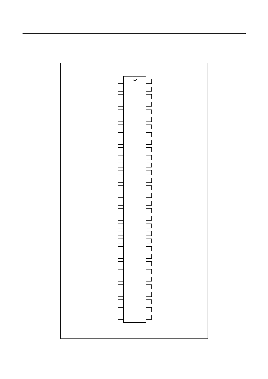
Fig. 4 Pin configuration (SDIP 64)
handbook, halfpage
XXX
MXXxxx
1
2
3
4
5
6
7
8
9
10
11
12
13
14
15
16
17
18
19
20
21
22
23
24
25
26
27
28
29
30
31
32
64
63
62
61
60
59
58
57
56
55
54
53
52
51
50
49
48
47
46
45
44
43
42
41
40
39
38
37
36
35
34
33
TDA955X/6X/8X PS/N1 series (SDIP-64)
P1.3/T1
P1.6/SCL
P1.7/SDA
P2.0/TPMW
P3.0/ADC0
P3.1/ADC1
P3.2/ADC2
P3.3/ADC3
VSSC/P
P0.5
P0.6
VSSA
SECPLL
VP2
DECDIG
HOUT
FBISO
PH2LF
PH1LF
GND3
AVL/EWD/
VDRB
VDRA
IFIN1
IFIN2
EHTO
IREF
VSC
AGCOUT
AUDEEM/SIFIN1
DECSDEM/SIFIN2
PLLIF
IFVO/SVO
DECBG
CVBS1
VP1
C
CVBS/Y
GND1
AUDOUT/AMOUT
AVL/SNDIF/REFO/
BLKIN
BO
GO
RO
BCLIN
R2/VIN
B2/UIN
G2/YIN
INSSW2
VDDA
VPE
VDDC
OSCGND
XTALIN
XTALOUT
RESET
VDDP
P1.0/INT1
P1.1/T0
P1.2/INT0
GND2
AMOUT
AUDEXT/QSSO/
SNDPLL/SIFAGC
AMOUT/AUDEEM/
DECSDEM
2000 Jun 22
13
Philips Semiconductors
Tentative Device Specification
TV signal processor-Teletext decoder with
embedded
µ
-Controller
TDA955X/6X/8X PS/N1 series
FUNCTIONAL DESCRIPTION OF THE 80C51
The functionality of the micro-controller used on this
device is described here with reference to the industry
standard 80C51 micro-controller. A full description of its
functionality can be found in the 80C51 based 8-bit
micro-controllers - Philips Semiconductors (ref. IC20).
Features of the 80c51
∑
80C51 micro-controller core standard instruction set and
timing.
∑
1
µ
s machine cycle.
∑
Maximum 128K x 8-bit Program ROM.
∑
Maximum of 12K x 8-bit Auxiliary RAM.
∑
2K (OSD only version) Auxiliary RAM, maximum
of 1.25K required for Display
∑
3K (1 page teletext version) Auxiliary RAM,
maximum of 2K required for Display
∑
12K (10 page teletext version) Auxiliary RAM,
maximum of 10K required for Display
∑
8-Level Interrupt Controller for individual enable/disable
with two level priority.
∑
Two 16-bit Timer/Counters.
∑
Additional 16-bit Timer with 8-bit Pre-scaler.
∑
WatchDog Timer.
∑
Auxiliary RAM Page Pointer.
∑
16-bit Data pointer
∑
Idle, Stand-by and Power-Down modes.
∑
13 General I/O.
∑
Four 6-bit Pulse Width Modulator (PWM) outputs for
control of TV analogue signals.
∑
One 14-bit PWM for Voltage Synthesis tuner control.
∑
8-bit ADC with 4 multiplexed inputs.
∑
2 high current outputs for directly driving LED's etc.
∑
I
2
C Byte Level bus interface.
Memory Organisation
The device has the capability of a maximum of 128K Bytes
of PROGRAM ROM and 12K Bytes of DATA RAM. The
OSD (& Closed Caption) only version has a 2K RAM and
a maximum of 64K ROM, the 1 page teletext version has
a 3K RAM and also a maximum of 64K ROM whilst the 10
page teletext version has a 12K RAM and a maximum of
128K ROM.
ROM Organisation
The 64K device has a continuous address space from 0 to
64K. The 128K is arranged in four banks of 32K. One of
the 32K banks is common and is always addressable. The
other three banks (Bank0, Bank1, Bank2) can be
accessed by selecting the right bank via the SFR ROMBK
bits 1/0.
RAM Organisation
The Internal Data RAM is organised into two areas, Data
Memory and Special Function Registers (SFRs) as shown
in Fig.6.
D
ATA
M
EMORY
The Data memory is 256 x 8-bits and occupies the address
range 00 to FF Hex when using Indirect addressing and 00
to 7F Hex when using direct addressing. The SFRs occupy
the address range 80 Hex to FF Hex and are accessible
using Direct addressing only. The lower 128 Bytes of Data
memory are mapped as shown in Fig.7. The lowest 32
Fig.5 ROM Bank Switching memory map
8000H
FFFFH
Bank0
32K
0000H
7FFFH
Common
32K
8000H
FFFFH
Bank1
32K
8000H
FFFFH
Bank2
32K
Accessible
by Direct
and Indirect
Addressing
Accessible
by Indirect
Addressing
only
Accessible
by Direct
Addressing
00H
7FH
80H
FFH
Lower
128
Upper
128
Data Memory
Special Function Registers
only
Fig.6 Internal Data Memory
2000 Jun 22
14
Philips Semiconductors
Tentative Device Specification
TV signal processor-Teletext decoder with
embedded
µ
-Controller
TDA955X/6X/8X PS/N1 series
bytes are grouped into 4 banks of 8 registers, the next 16 bytes above the register banks form a block of bit addressable
memory space. The upper 128 bytes are not allocated for any special area or functions.
SFR M
EMORY
The Special Function Register (SFR) space is used for port latches, counters/timers, peripheral control, data capture and
display. These registers can only be accessed by direct addressing. Sixteen of the addresses in the SFR space are both
bit and byte addressable. The bit addressable SFRs are those whose address ends in 0H or 8H. A summary of the SFR
map in address order is shown in Table 2.
ADD
R/W
Names
BIT7
BIT6
BIT5
BIT4
BIT3
BIT2
BIT1
BIT0
80H
R/W
P0
Reserved
P0<6>
P0<5>
Reserved
Reserved
Reserved
Reserved
Reserved
81H
R/W
SP
SP<7>
SP<6>
SP<5>
SP<4>
SP<3>
SP<2>
SP<1>
SP<0>
82H
R/W
DPL
DPL<7>
DPL<6>
DPL<5>
DPL<4>
DPL<3>
DPL<2>
DPL<1>
DPL<0>
83H
R/W
DPH
DPH<7>
DPH<6>
DPH<5>
DPH<4>
DPH<3>
DPH<2>
DPH<1>
DPH<0>
84H
R/W
IEN1
-
-
-
-
-
-
-
ET2
85H
R/W
IP1
-
-
-
-
-
-
-
PT2
87H
R/W
PCON
0
ARD
RFI
WLE
GF1
GF0
PD
IDL
88H
R/W
TCON
TF1
TR1
TF0
TR0
IE1
IT1
IE0
IT0
89H
R/W
TMOD
GATE
C/T
M1
M0
GATE
C/T
M1
M0
8AH
R/W
TL0
TL0<7>
TL0<6>
TL0<5>
TL0<4>
TL0<3>
TL0<2>
TL0<1>
TL0<0>
8BH
R/W
TL1
TL1<7>
TL1<6>
TL1<5>
TL1<4>
TL1<3>
TL1<2>
TL1<1>
TL1<0>
8CH
R/W
TH0
TH0<7>
TH0<6>
TH0<5>
TH0<4>
TH0<3>
TH0<2>
TH0<1>
TH0<0>
8DH
R/W
TH1
TH1<7>
TH1<6>
TH1<5>
TH1<4>
TH1<3>
TH1<2>
TH1<1>
TH1<0>
90H
R/W
P1
P1<7>
P1<6>
Reserved
Reserved
P1<3>
P1<2>
P1<1>
P1<0>
91H
R/W
TP2L
TP2L<7>
TP2L<6>
TP2L<5>
TP2L<4>
TP2L<3>
TP2L<2>
TP2L<1>
TP2L<0>
Table 2
SFR Map
Bank Select
Bits in PSW
00H
08H
10H
18H
20H
07H
0FH
17H
1FH
2FH
11 = BANK3
7FH
10 = BANK2
01 = BANK1
00 = BANK0
Bit Addressable Space
(
Bit Addresses 0-7F)
4 Banks of 8 Registers
R0 - R7
Fig.7
Lower 128 Bytes of Internal RAM

2000 Jun 22
15
Philips Semiconductors
Tentative Device Specification
TV signal processor-Teletext decoder with
embedded
µ
-Controller
TDA955X/6X/8X PS/N1 series
92H
R/W
TP2H
TP2H<15>
TP2H<14>
TP2H<13>
TP2H<12>
TP2H<11>
TP2H<10>
TP2H<9>
TP2H<8>
93H
R/W
TP2PR
TP2PR<7>
TP2PR<6>
TP2PR<5>
TP2PR<4>
TP2PR<3>
TP2PR<2>
TP2PR<1>
TP2PR<0>
94H
R/W
TP2CRL
-
-
-
-
-
-
TP2CRL<1>
TP2CRL<0>
96H
R/W
P0CFGA
Reserved
P0CFGA<6>
P0CFGA<5>
Reserved
Reserved
Reserved
Reserved
Reserved
97H
R/W
P0CFGB
Reserved
P0CFGB<6>
P0CFGB<5>
Reserved
Reserved
Reserved
Reserved
Reserved
98H
R/W
SADB
-
-
-
DC_COMP
SAD<3>
SAD<2>
SAD<1>
SAD<0>
9CH
R
TP2CL
TP2CL<7>
TP2CL<6>
TP2CL<5>
TP2CL<4>
TP2CL<3>
TP2CL<2>
TP2CL<1>
TP2CL<0>
9DH
R
TP2CH
TP2CH<7>
TP2CH<6>
TP2CH<5>
TP2CH<4>
TP2CH<3>
TP2CH<2>
TP2CH<1>
TP2CH<0>
9EH
R/W
P1CFGA
P1CFGA<7>
P1CFGA<6>
Reserved
Reserved
P1CFGA<3>
P1CFGA<2>
P1CFGA<1>
P1CFGA<0>
9FH
R/W
P1CFGB
P1CFGB<7>
P1CFGB<6>
Reserved
Reserved
P1CFGB<3>
P1CFGB<2>
P1CFGB<1>
P1CFGB<0>
A0H
R/W
P2
Reserved
-
-
-
-
-
-
P2<0>
A6H
R/W
P2CFGA
Reserved
P2CFGA<6>
P2CFGA<5>
P2CFGA<4>
P2CFGA<3>
P2CFGA<2>
P2CFGA<1>
P2CFGA<0>
A7H
R/W
P2CFGB
Reserved
P2CFGB<6>
P2CFGB<5>
P2CFGB<4>
P2CFGB<3>
P2CFGB<2>
P2CFGB<1>
P2CFGB<0>
A8H
R/W
IE
EA
EBUSY
ES2
ECC
ET1
EX1
ET0
EX0
B0H
R/W
P3
Reserved
Reserved
Reserved
Reserved
P3<3>
P3<2>
P3<1>
P3<0>
B2H
R/W
TXT18
NOT<3>
NOT<2>
NOT<1>
NOT<0>
0
0
BS<1>
BS<0>
B3H
R/W
TXT19
TEN
TC<2>
TC<1>
TC<0>
0
0
TS<1>
TS<0>
B4H
R/W
TXT20
DRCS
ENABLE
OSD
PLANES
0
0
OSD LANG
ENABLE
OSD
LAN<2>
OSD
LAN<1>
OSD
LAN<0>
B5H
R/W
TXT21
DISP
LINE<1>
DISP
LINES<0>
CHAR
SIZE<1>
CHAR
SIZE<0>
Reserved
CC ON
I2C PORT0
CC/TXT
B6H
R
TXT22
GPF1<7>
GPF1<6>
GPF1<5>
GPF1<4>
GPF1<3>
GPF1<2>
GPF1<1>
GPF1<0>
B7H
R/W
CCLIN
0
0
0
CS<4>
CS<3>
CS<2>
CS<1>
CS<0>
B8H
R/W
IP
0
PBUSY
PES2
PCC
PT1
PX1
PT0
PX0
B9H
R/W
TXT17
0
FORCE
ACQ<1>
FORCE
ACQ<0>
FORCE
DISP<1>
FORCE
DISP<0>
SCREEN
COL<2>
SCREEN
COL<1>
SCREEN
COL<0>
BAH
R
WSS1
0
0
0
WSS<3:0>
ERROR
WSS<3>
WSS<2>
WSS<1>
WSS<0>
BBH
R
WSS2
0
0
0
WSS<7:4>
ERROR
WSS<7>
WSS<6>
WSS<5>
WSS<4>
BCH
R
WSS3
WSS<13:11>
ERROR
WSS<13>
WSS<12>
WSS<11>
WSS<10:8>
ERROR
WSS<10>
WSS<9>
WSS<8>
BEH
R/W
P3CFGA
Reserved
Reserved
Reserved
Reserved
P3CFGA<3>
P3CFGA<2>
P3CFGA<1>
P3CFGA<0>
BFH
R/W
P3CFGB
Reserved
Reserved
Reserved
Reserved
P3CFGB<3>
P3CFGB<2>
P3CFGB<1>
P3CFGB<0>
C0H
R/W
TXT0
X24 POSN
DISPLAY
X24
AUTO
FRAME
DISABLE
HEADER
ROLL
DISPLAY
STATUS
ROW ONLY
DISABLE
FRAME
VPS ON
INV ON
ADD
R/W
Names
BIT7
BIT6
BIT5
BIT4
BIT3
BIT2
BIT1
BIT0
Table 2
SFR Map

2000 Jun 22
16
Philips Semiconductors
Tentative Device Specification
TV signal processor-Teletext decoder with
embedded
µ
-Controller
TDA955X/6X/8X PS/N1 series
C1H
R/W
TXT1
EXT PKT
OFF
8 BIT
ACQ OFF
X26 OFF
FULL
FIELD
FIELD
POLARITY
H
POLARITY
V
POLARITY
C2H
R/W
TXT2
ACQ BANK
REQ<3>
REQ<2>
REQ<1>
REQ<0>
SC<2>
SC<1>
SC<0>
C3H
W
TXT3
-
-
-
PRD<4>
PRD<3>
PRD<2>
PRD<1>
PRD<0>
C4H
R/W
TXT4
OSD BANK
ENABLE
QUAD
WIDTH
ENABLE
EAST/WES
T
DISABLE
DOUBLE
HEIGHT
B MESH
ENABLE
C MESH
ENABLE
TRANS
ENABLE
SHADOW
ENABLE
C5H
R/W
TXT5
BKGND
OUT
BKGND IN
CORB OUT
CORB IN
TEXT OUT
TEXT IN
PICTURE
ON OUT
PICTURE
ON IN
C6H
R/W
TXT6
BKGND
OUT
BKGND IN
CORB OUT
CORB IN
TEXT OUT
TEXT IN
PICTURE
ON OUT
PICTURE
ON IN
C7H
R/W
TXT7
STATUS
ROW TOP
CURSOR
ON
REVEAL
BOTTOM/
TOP
DOUBLE
HEIGHT
BOX ON 24
BOX ON
1-23
BOX ON 0
C8H
R/W
TXT8
(Reserved)
0
FLICKER
STOP ON
HUNT
DISABLE
SPANISH
PKT 26
RECEIVED
WSS
RECEIVED
WSS ON
CVBS1/
CVBS0
C9H
R/W
TXT9
CURSOR
FREEZE
CLEAR
MEMORY
A0
R<4>
R<3>
R<2>
R<1>
R<0>
CAH
R/W
TXT10
0
0
C<5>
C<4>
C<3>
C<2>
C<1>
C<0>
CBH
R/W
TXT11
D<7>
D<6>
D<5>
D<4>
D<3>
D<2>
D<1>
D<0>
CCH
R
TXT12
525/625
SYNC
ROM
VER<4>
ROM
VER<3>
ROM
VER<2>
ROM
VER<1>
ROM
VER<0>
1
VIDEO
SIGNAL
QUALITY
CDH
R/W
TXT14
0
0
0
DISPLAY
BANK
PAGE<3>
PAGE<2>
PAGE<1>
PAGE<0>
CEH
R/W
TXT15
0
0
0
MICRO
BANK
BLOCK<3>
BLOCK<2>
BLOCK<1>
BLOCK<0>
D0H
R/W
PSW
C
AC
F0
RS1
RS0
OV
-
P
D2H
R/W
TDACL
TD<7>
TD<6>
TD<5>
TD<4>
TD<3>
TD<2>
TD<1>
TD<0>
D3H
R/W
TDACH
TPWE
1
TD<13>
TD<12>
TD<11>
TD<10>
TD<9>
TD<8>
D5H
R/W
PWM0
PW0E
1
PW0V<5>
PW0V<4>
PW0V<3>
PW0V<2>
PW0V<1>
PW0V<0>
D6H
R/W
PWM1
PW1E
1
PW1V<5>
PW1V<4>
PW1V<3>
PW1V<2>
PW1V<1>
PW1V<0>
D7H
R
CCDAT1
CCD1<7>
CCD1<6>
CCD1<5>
CCD1<4>
CCD1<3>
CCD1<2>
CCD1<1>
CCD1<0>
D8H
R/W
S1CON
CR<2>
ENSI
STA
STO
SI
AA
CR<1>
CR<0>
D9H
R
S1STA
STAT<4>
STAT<3>
STAT<2>
STAT<1>
STAT<0>
0
0
0
DAH
R/W
S1DAT
DAT<7>
DAT<6>
DAT<5>
DAT<4>
DAT<3>
DAT<2>
DAT<1>
DAT<0>
DBH
R/W
S1ADR
ADR<6>
ADR<5>
ADR<4>
ADR<3>
ADR<2>
ADR<1>
ADR<0>
GC
DCH
R/W
PWM3
PW3E
1
PW3V<5>
PW3V<4>
PW3V<3>
PW3V<2>
PW3V<1>
PW3V<0>
E0H
R/W
ACC
ACC<7>
ACC<6>
ACC<5>
ACC<4>
ACC<3>
ACC<2>
ACC<1>
ACC<0>
E4H
R/W
PWM2
PW2E
1
PW2V<5>
PW2V<4>
PW2V<3>
PW2V<2>
PW2V<1>
PW2V<0>
ADD
R/W
Names
BIT7
BIT6
BIT5
BIT4
BIT3
BIT2
BIT1
BIT0
Table 2
SFR Map

2000 Jun 22
17
Philips Semiconductors
Tentative Device Specification
TV signal processor-Teletext decoder with
embedded
µ
-Controller
TDA955X/6X/8X PS/N1 series
A description of each of the SFR bits is shown in Table 3, The SFRs are in alphabetical order.
E7H
R
CCDAT2
CCD2<7>
CCD2<6>
CCD2<5>
CCD2<4>
CCD2<3>
CCD2<2>
CCD2<1>
CCD2<0>
E8H
R/W
SAD
VHI
CH<1>
CH<0>
ST
SAD<7>
SAD<6>
SAD<5>
SAD<4>
F0H
R/W
B
B<7>
B<6>
B<5>
B<4>
B<3>
B<2>
B<1>
B<0>
F8H
R/W
TXT13
VPS
RECEIVED
PAGE
CLEARING
525
DISPLAY
525 TEXT
625 TEXT
PKT 8/30
FASTEXT
0
FAH
R/W
XRAMP
XRAMP<7>
XRAMP<6>
XRAMP<5>
XRAMP<4>
XRAMP<3>
XRAMP<2>
XRAMP<1>
XRAMP<0>
FBH
R/W
ROMBK
STANDBY
IIC_LUT<1>
IIC_LUT<0>
0
0
0
ROMBK<1>
ROMBK<0>
FDH
R
TEST
TEST<7>
TEST<6>
TEST<5>
TEST<4>
TEST<3>
TEST<2>
TEST<1>
TEST<0>
FEH
W
WDTKEY
WKEY<7>
WKEY<6>
WKEY<5>
WKEY<4>
WKEY<3>
WKEY<2>
WKEY<1>
WKEY<0>
FFH
R/W
WDT
WDV<7>
WDV<6>
WDV<5>
WDV<4>
WDV<3>
WDV<2>
WDV<1>
WDV<0>
Names
BIT7
BIT6
BIT5
BIT4
BIT3
BIT2
BIT1
BIT0
RESET
ACC
ACC<7>
ACC<6>
ACC<5>
ACC<4>
ACC<3>
ACC<2>
ACC<1>
ACC<0>
00H
ACC<7:0>
Accumulator value.
B
B<7>
B<6>
B<5>
B<4>
B<3>
B<2>
B<1>
B<0>
00H
B<7:0>
B Register value.
CCDAT1
CCD1<7>
CCD1<6>
CCD1<5>
CCD1<4>
CCD1<3>
CCD1<2>
CCD1<1>
CCD1<0>
00H
CCD1<7:0>
Closed Caption first data byte.
CCDAT2
CCD2<7>
CCD2<6>
CCD2<5>
CCD2<4>
CCD2<3>
CCD2<2>
CCD2<1>
CCD2<0>
00H
CCD2<7:0>
Closed Caption second data byte.
CCLIN
0
0
0
CS<4>
CS<3>
CS<2>
CS<1>
CS<0>
15H
CS<4:0>
Closed Caption Slice line using 525 line number.
DPH
DPH<7>
DPH<6>
DPH<5>
DPH<4>
DPH<3>
DPH<2>
DPH<1>
DPH<0>
00H
DPH<7:0>
Data Pointer High byte, used with DPL to address display and auxiliary memory.
DPL
DPL<7>
DPL<6>
DPL<5>
DPL<4>
DPL<3>
DPL<2>
DPL<1>
DPL<0>
00H
DPL<7:0>
Data pointer low byte, used with DPH to address display and auxiliary memory.
IE
EA
EBUSY
ES2
ECC
ET1
EX1
ET0
EX0
00H
EA
Disable all interrupts (0), or use individual interrupt enable bits (1).
EBUSY
Enable BUSY Interrupt.
ES2
Enable I
2
C Interrupt.
ECC
Enable Closed Caption Interrupt.
Table 3
SFR Bit description
ADD
R/W
Names
BIT7
BIT6
BIT5
BIT4
BIT3
BIT2
BIT1
BIT0
Table 2
SFR Map

2000 Jun 22
18
Philips Semiconductors
Tentative Device Specification
TV signal processor-Teletext decoder with
embedded
µ
-Controller
TDA955X/6X/8X PS/N1 series
ET1
Enable Timer 1 Interrupt.
EX1
Enable External Interrupt 1.
ET0
Enable Timer 0 Interrupt.
EX0
Enable External Interrupt 0.
IEN1
-
-
-
-
-
-
-
ET2
00H
ET2
Enable Timer 2 Interrupt.
IP
0
PBUSY
PES2
PCC
PT1
PX1
PT0
PX0
00H
PBUSY
Priority EBUSY Interrupt.
PES2
Priority ES2 Interrupt.
PCC
Priority ECC Interrupt.
PT1
Priority Timer 1 Interrupt.
PX1
Priority External Interrupt 1.
PT0
Priority Timer 0 Interrupt.
PX0
Priority External Interrupt 0.
IP1
-
-
-
-
-
-
-
PT2
00H
PT2
Priority Timer 2 Interrupt.
P0
Reserved
P0<6>
P0<5>
Reserved
Reserved
Reserved
Reserved
Reserved
FFH
P0<6:5>
Port 0 I/O register connected to external pins.
P1
P1<7>
P1<6>
Reserved
Reserved
P1<3>
P1<2>
P1<1>
P1<0>
FFH
P1<7:6>
Port 1 I/O register connected to external pins.
P1<3:0>
Port 1 I/O register connected to external pins.
P2
Reserved
P2<6>
P2<5>
P2<4>
P2<3>
P2<2>
P2<1>
P2<0>
FFH
P2<6:0>
Port 2 I/O register connected to external pins.
P3
Reserved
Reserved
Reserved
Reserved
P3<3>
P3<2>
P3<1>
P3<0>
FFH
P3<3:0>
Port 3 I/O register connected to external pins.
P0CFGA
Reserved
P0CFGA<6>
P0CFGA<5>
Reserved
Reserved
Reserved
Reserved
Reserved
FFH
P0CFGB
Reserved
P0CFGB<6>
P0CFGB<5>
Reserved
Reserved
Reserved
Reserved
Reserved
00H
P0CFGB<x>/P0CFGA<x> = 00
MODE 0 Open Drain.
P0CFGB<x>/P0CFGA<x> = 01
MODE 1 Quasi Bi-Directional.
P0CFGB<x>/P0CFGA<x> = 10
MODE2 High Impedance.
P0CFGB<x>/P0CFGA<x> = 11
MODE3 Push Pull.
P1CFGA
P1CFGA<7>
P1CFGA<6>
Reserved
Reserved
P1CFGA<3>
P1CFGA<2>
P1CFGA<1>
P1CFGA<0>
FFH
P1CFGB
P1CFGB<7>
P1CFGB<6>
Reserved
Reserved
P1CFGB<3>
P1CFGB<2>
P1CFGB<1>
P1CFGB<0>
00H
Names
BIT7
BIT6
BIT5
BIT4
BIT3
BIT2
BIT1
BIT0
RESET
Table 3
SFR Bit description

2000 Jun 22
19
Philips Semiconductors
Tentative Device Specification
TV signal processor-Teletext decoder with
embedded
µ
-Controller
TDA955X/6X/8X PS/N1 series
P1CFGB<x>/P1CFGA<x> = 00
MODE 0 Open Drain.
P1CFGB<x>/P1CFGA<x> = 01
MODE 1 Quasi Bi-Directional.
P1CFGB<x>/P1CFGA<x> = 10
MODE2 High Impedance.
P1CFGB<x>/P1CFGA<x> = 11
MODE3 Push Pull.
P2CFGA
Reserved
P2CFGA<6>
P2CFGA<5>
P2CFGA<4>
P2CFGA<3>
P2CFGA<2>
P2CFGA<1>
P2CFGA<0>
FFH
P2CFGB
Reserved
P2CFGB<6>
P2CFGB<5>
P2CFGB<4>
P2CFGB<3>
P2CFGB<2>
P2CFGB<1>
P2CFGB<0>
00H
P2CFGB<x>/P2CFGA<x> = 00
MODE 0 Open Drain.
P2CFGB<x>/P2CFGA<x> = 01
MODE 1 Quasi Bi-Directional.
P2CFGB<x>/P2CFGA<x> = 10
MODE2 High Impedance.
P2CFGB<x>/P2CFGA<x> = 11
MODE3 Push Pull.
P3CFGA
Reserved
Reserved
Reserved
Reserved
P3CFGA<3>
P3CFGA<2>
P3CFGA<1>
P3CFGA<0>
FFH
P3CFGB
Reserved
Reserved
Reserved
Reserved
P3CFGB<3>
P3CFGB<2>
P3CFGB<1>
P3CFGB<0>
00H
P3CFGB<x>/P3CFGA<x> = 00
MODE 0 Open Drain.
P3CFGB<x>/P3CFGA<x> = 01
MODE 1 Quasi Bi-directional.
P3CFGB<x>/P3CFGA<x> = 10
MODE2 High Impedance.
P3CFGB<x>/P3CFGA<x> = 11
MODE3 Push Pull.
PCON
SMOD
ARD
RFI
WLE
GF1
GF0
PD
IDL
00H
SMOD
UART Baud Rate Double Control.
ARD
Auxiliary RAM Disable, All MOVX instructions access the external data memory.
RFI
Disable ALE during internal access to reduce Radio Frequency Interference.
WLE
Watch Dog Timer enable.
GF1
General purpose flag.
GF0
General purpose flag.
PD
Power-down activation bit.
IDL
Idle mode activation bit.
PSW
C
AC
F0
RS<1>
RS<0>
OV
-
P
00H
C
Carry Bit.
AC
Auxiliary Carry bit.
F0
Flag 0, General purpose flag.
RS<1:0>
Register Bank selector bits.
RS<1:0> = 00, Bank0 (00H - 07H).
RS<1:0> = 01, Bank1 (08H - 0FH).
RS<1:0> = 10, Bank2 (10H - 17H).
RS<1:0> = 11, Bank3 (18H - 1FH).
OV
Overflow flag.
Names
BIT7
BIT6
BIT5
BIT4
BIT3
BIT2
BIT1
BIT0
RESET
Table 3
SFR Bit description

2000 Jun 22
20
Philips Semiconductors
Tentative Device Specification
TV signal processor-Teletext decoder with
embedded
µ
-Controller
TDA955X/6X/8X PS/N1 series
P
Parity bit.
PWM0
PW0E
1
PW0V<5>
PW0V<4>
PW0V<3>
PW0V<2>
PW0V<1>
PW0V<0>
40H
PW0E
0 - Disable Pulse Width Modulator 0.
1 - Enable Pulse Width Modulator 0.
PW0V<5:0>
Pulse Width Modulator high time.
PWM1
PW1E
1
PW1V<5>
PW1V<4>
PW1V<3>
PW1V<2>
PW1V<1>
PW1V<0>
40H
PW1E
0 - Disable Pulse Width Modulator 1.
1 - Enable Pulse Width Modulator 1.
PW1V<5:0>
Pulse Width Modulator high time.
PWM2
PW2E
1
PW2V<5>
PW2V<4>
PW2V<3>
PW2V<2>
PW2V<1>
PW2V<0>
40H
PW2E
0 - Disable Pulse Width Modulator 2.
1 - Enable Pulse Width Modulator 2.
PW2V<5:0>
Pulse Width Modulator high time.
PWM3
PW3E
1
PW3V<5>
PW3V<4>
PW3V<3>
PW3V<2>
PW3V<1>
PW3V<0>
40H
PW3E
0 - Disable Pulse Width Modulator 3.
1 - Enable Pulse Width Modulator 3.
PW3V<5:0>
Pulse Width Modulator high time.
ROMBK
STANDBY
IIC_LUT<1>
IIC_LUT<0>
0
0
0
ROMBK<1>
ROMBK<0>
00H
STANDBY
0 - Disable Stand-by Mode
1 - Enable Stand-by Mode
IIC_LUT<1:0>
IIC Lookup table selection:
IIC_LUT<1:0>=00, 558 Normal Mode.
IIC_LUT<1:0>=01, 558 Fast Mode.
IIC_LUT<1:0>=10, 558 Slow Mode.
IIC_LUT<1:0>=11, Reserved.
ROMBK<1:0>
ROM Bank selection
ROMBK<1:0>=00, Bank0
ROMBK<1:0>=01, Bank1
ROMBK<1:0>=10, Bank2
ROMBK<1:0>=11, Reserved
S1ADR
ADR<6>
ADR<5>
ADR<4>
ADR<3>
ADR<2>
ADR<1>
ADR<0>
GC
00H
ADR<6:0>
I2C Slave Address.
GC
0 - Disable I
2
C general call address.
1 - Enable I
2
C general call address.
S1CON
CR<2>
ENSI
STA
STO
SI
AA
CR<1>
CR<0>
00H
CR<2:0>
Clock rate bits.
IIC rates are selectable (three tables)
ENSI
0 - Disable I
2
C interface.
1 - Enable I
2
C interface.
Names
BIT7
BIT6
BIT5
BIT4
BIT3
BIT2
BIT1
BIT0
RESET
Table 3
SFR Bit description

2000 Jun 22
21
Philips Semiconductors
Tentative Device Specification
TV signal processor-Teletext decoder with
embedded
µ
-Controller
TDA955X/6X/8X PS/N1 series
STA
START flag. When this bit is set in slave mode, the hardware checks the I2C bus and generates a START condition if the bus is free or after the bus
becomes free. If the device operates in master mode it will generate a repeated START condition.
STO
STOP flag. If this bit is set in a master mode a STOP condition is generated. A STOP condition detected on the I2C bus clears this bit. This bit may
also be set in slave mode in order to recover from an error condition. In this case no STOP condition is generated to the I2C bus, but the hardware
releases the SDA and SCL lines and switches to the not selected receiver mode. The STOP flag is cleared by the hardware.
SI
Serial Interrupt flag. This flag is set and an interrupt request is generated, after any of the following events occur:
-A START condition is generated in master mode.
-The own slave address has been received during AA=1.
-The general call address has been received while S1ADR.GC and AA=1.
-A data byte has been received or transmitted in master mode (even if arbitration is lost).
-A data byte has been received or transmitted as selected slave.
A STOP or START condition is received as selected slave receiver or transmitter
While the SI flag is set, SCL remains LOW and the serial transfer is suspened.SI must be reset by software.
AA
Assert Acknowledge flag. When this bit is set, an acknowledge is returned after any one of the following conditions
-Own slave address is received.
-General call address is received(S1ADR.GC=1).
-A data byte is received, while the device is programmed to be a master receiver.
-A data byte is received, while the device is selected slave receiver.
When the bit is reset, no acknowledge is returned. Consequently, no interrupt is requested when the own address or general call address is
received.
S1DAT
DAT<7>
DAT<6>
DAT<5>
DAT<4>
DAT<3>
DAT<2>
DAT<1>
DAT<0>
00H
DAT<7:0>
I
2
C Data.
S1STA
STAT<4>
STAT<3>
STAT<2>
STAT<1>
STAT<0>
0
0
0
F8H
STAT<4:0>
I
2
C Interface Status.
SAD
VHI
CH<1>
CH<0>
ST
SAD<7>
SAD<6>
SAD<5>
SAD<4>
00H
VHI
0 - Analogue input voltage less than or equal to DAC voltage.
1 - Analogue input voltage greater then DAC voltage.
CH<1:0>
ADC Input channel select.
CH<1:0> = 00,ADC3.
CH<1:0> = 01,ADC0.
CH<1:0> = 10,ADC1.
CH<1:0> = 11,ADC2.
ST
Initiate voltage comparison between ADC input Channel and SADB<3:0> value.
Note: Set by Software and reset by Hardware.
SAD<7:4>
Most Significant nibble of DAC input word
SADB
0
0
0
DC_COMP
SAD<3>
SAD<2>
SAD<1>
SAD<0>
00H
DC_COMP
0 - Disable DC Comparator mode.
1 - Enable DC Comparator mode.
SAD<3:0>
4-bit SAD value.
SP
SP<7>
SP<6>
SP<5>
SP<4>
SP<3>
SP<2>
SP<1>
SP<0>
07H
SP<7>
Stack Pointer.
TCON
TF1
TR1
TF0
TR0
IE1
IT1
IE0
IT0
00H
TF1
Timer 1 overflow Flag. Set by hardware on Timer/Counter overflow.Cleared by hardware when processor vectors to interrupt routine.
Names
BIT7
BIT6
BIT5
BIT4
BIT3
BIT2
BIT1
BIT0
RESET
Table 3
SFR Bit description

2000 Jun 22
22
Philips Semiconductors
Tentative Device Specification
TV signal processor-Teletext decoder with
embedded
µ
-Controller
TDA955X/6X/8X PS/N1 series
TR1
Timer 1 Run control bit. Set/Cleared by software to turn Timer/Counter on/off.
TF0
Timer 0 overflow Flag. Set by hardware on Timer/Counter overflow.Cleared by hardware when processor vectors to interrupt routine.
TR0
Timer 0 Run control bit. Set/Cleared by software to turn Timer/Counter on/off.
IE1
Interrupt 1 Edge flag (both edges generate flag). Set by hardware when external interrupt edge detected.Cleared by hardware when interrupt
processed.
IT1
Interrupt 1 Type control bit. Set/Cleared by Software to specify edge/low level triggered external interrupts.
IE0
Interrupt 0 Edge l flag. Set by hardware when external interrupt edge detected.Cleared by hardware when interrupt processed.
IT0
Interrupt 0 Type flag.Set/Cleared by Software to specify falling edge/low level triggered external interrupts.
TDACH
TPWE
1
TD<13>
TD<12>
TD<11>
TD<10>
TD<9>
TD<8>
40H
TPWE
0 - Disable Tuning Pulse Width Modulator.
1 - Enable Tuning Pulse Width Modulator.
TD<13:8>
Tuning Pulse Width Modulator High Byte.
TDACL
TD<7>
TD<6>
TD<5>
TD<4>
TD<3>
TD<2>
TD<1>
TD<0>
00H
TD<7:0>
Tuning Pulse Width Modulator Low Byte.
TH0
TH0<7>
TH0<6>
TH0<5>
TH0<4>
TH0<3>
TH0<2>
TH0<1>
TH0<0>
00H
TH0<7:0>
Timer 0 high byte.
TH1
TH1<7>
TH1<6>
TH1<5>
TH1<4>
TH1<3>
TH1<2>
TH1<1>
TH1<0>
00H
TH1<7:0>
Timer 1 high byte.
TL0
TL0<7>
TL0<6>
TL0<5>
TL0<4>
TL0<3>
TL0<2>
TL0<1>
TL0<0>
00H
TL0<7:0>
Timer 0 low byte.
TL1
TL1<7>
TL1<6>
TL1<5>
TL1<4>
TL1<3>
TL1<2>
TL1<1>
TL1<0>
00H
TL1<7:0>
Timer 1 low byte.
TMOD
GATE
C/T
M1
M0
GATE
C/T
M1
M0
00H
Timer / Counter 1
Timer / Counter 0
GATE
Gating Control Timer /Counter 1.
C/T
Counter/Timer 1 selector.
M1,M0
Mode control bits Timer/Counter 1.
M1,M0 = 00, 8 bit timer or 8 bit counter with divide by 32 pre-scaler.
M1,M0 = 01, 16 bit time interval or event counter.
M1,M0 = 10, 8 bit time interval or event counter with automatic reload upon overflow. Reload value stored in TH1.
M1,M0 = 11, stopped.
GATE
Gating control Timer/Counter 0.
C/T
Counter/Timer 0 selector.
Names
BIT7
BIT6
BIT5
BIT4
BIT3
BIT2
BIT1
BIT0
RESET
Table 3
SFR Bit description

2000 Jun 22
23
Philips Semiconductors
Tentative Device Specification
TV signal processor-Teletext decoder with
embedded
µ
-Controller
TDA955X/6X/8X PS/N1 series
M1,M0
Mode Control bits Timer/Counter 0.
M1,M0 = 00, 8 bit timer or 8 bit counter with divide by 32 pre-scaler.
M1,M0 = 01, 16 bit time interval or event counter.
M1,M0 = 10, 8 bit time interval or event counter with automatic reload upon overflow. Reload value stored in TH0.
M1,M0 = 11, one 8 bit time interval or event counter and one 8 bit time interval counter.
TP2CL
TP2CL<7>
TP2CL<6>
TP2CL<5>
TP2CL<4>
TP2CL<3>
TP2CL<2>
TP2CL<1>
TP2CL<0>
00H
TP2CL<7:0>
Indicate the low byte of the Time 2 current value.
TP2CH
TP2CH<7>
TP2CH<6>
TP2CH<5>
TP2CH<4>
TP2CH<3>
TP2CH<2>
TP2CH<1>
TP2CH<0>
00H
TP2CH<7:0>
Indicate the high byte of the Time 2 current value.
TP2H
TP2H<7>
TP2H<6>
TP2H<5>
TP2H<4>
TP2H<3>
TP2H<2>
TP2H<1>
TP2H<0>
00H
TP2H<7:0>
Timer 2 high byte, never change unless updated by the software.
TP2L
TP2L<7>
TP2L<6>
TP2L<5>
TP2L<4>
TP2L<3>
TP2L<2>
TP2L<1>
TP2L<0>
00H
TP2L<7:0>
Timer 2 low byte, never change unless updated by the software.
TP2PR
TP2PR<7>
TP2PR<6>
TP2PR<5>
TP2PR<4>
TP2PR<3>
TP2PR<2>
TP2PR<1>
TP2PR<0>
00H
TP2H<7:0>
Timer 2 Pre-scaler, never change unless updated by the software.
TP2CRL
-
-
-
-
-
-
TP2CRL<1>
TP2CRL<0>
00H
TP2CRL<0>
Timer 2 Control.
0 - Timer 2 disabled.
1 - Timer 2 enabled.
TP2CRL<1>
Timer 2 Status.
0 - No Overflow.
1 - Overflow.
TEST
TEST<7>
TEST<6>
TEST<5>
TEST<4>
TEST<3>
TEST<2>
TEST<1>
TEST<0>
00H
TEST<2:0>
Program Type bit SEL<2:0>.
011 - Display Dram test.
001 - Acquisition1 test.
010 - Acquisition2 test
TEST<4:3>
Functional test mode bits, set via mode select logic.
TEST<7:5>
Dram Size.
000 - 1.5K x 16.
001 - 2K x 16.
010 - 6K x 16.
011 - 7K x 16.
100 - 12K x 16.
101 - 14K x 16.
110 - 1K x 16.
111 - 11K x 16.
TXT0
X24 POSN
DISPLAY
X24
AUTO
FRAME
DISABLE
HEADER
ROLL
DISPLAY
STATUS
ROW
ONLY
DISABLE
FRAME
VPS ON
INV ON
00H
X24 POSN
0 - Store X/24 in extension memory
1 - Store X/24 in basic page memory with packets 0 to 23
Names
BIT7
BIT6
BIT5
BIT4
BIT3
BIT2
BIT1
BIT0
RESET
Table 3
SFR Bit description

2000 Jun 22
24
Philips Semiconductors
Tentative Device Specification
TV signal processor-Teletext decoder with
embedded
µ
-Controller
TDA955X/6X/8X PS/N1 series
DISLAY X24
0 - Display row 24 from basic page memory
1 - Display row 24 from appropriate location in extension memory
AUTO FRAME
0 - Normal Frame output
1 - Frame output is switched off automatically if any video displayed
DISABLE
HEADER ROLL
0 - Write rolling headers and time to current display page
1 - Disable writing of rolling headers and time to into memory
DISPLAY
STATUS ROW
ONLY
0 - Display normal page rows 0 to 24
1- Display only row 24
DISABLE
FRAME
0 - Normal Frame output
1 - Force Frame output to be low (0)
VPS ON
0 - VPS acquisition off
1 - VPS acquisition on
INV ON
0 - Inventory page off
1 - Inventory page on
TXT1
EXT PKT
OFF
8 BIT
ACQ OFF
ACQ OFF
FULL
FIELD
FIELD
POLARITY
H
POLARITY
V
POLARITY
00H
EXT PKT OFF
0 - Acquire extension packets X/24,X/27,8/30/X
1 - Disable acquisition of extension packets
8 BIT
0 - Error check and/or correct packets 0 to 24
1 - Disable checking of packets 0 to 24 written into memory
ACQ OFF
0 - Write requested data into display memory
1 - Disable writing of data into Display memory
X26 OFF
0 - Enable automatic processing of X/26 data
1 - Disable automatic processing of X/26 data
FULL FIELD
0 - Acquire CC data only on selected line.
1 - Acquire CC data on any TV line (for test purposes).
FIELD POLARIY
0 - Vsync pulse in first half of line during even field.
1 - Vsync pulse in second half of line during even field.
H POLARITY
0 - Hsync reference edge is positive going
1 - Hsync reference edge is negative going
V POLARITY
0 - Vsync reference edge is positive going
1 - Vsync reference edge is negative going
TXT2
ACQ
BANK
REQ<3>
REQ<2>
REQ<1>
REQ<0>
SC<2>
SC<1>
SC<0>
00H
ACQ_BANK
0 - Select Acquisition bank 0
1 - Select Acquisition bank 1
REQ<3:0>
Page request
SC<2:0>
Start column of page request
TXT3
PRD<4>
PRD<3>
PRD<2>
PRD<1>
PRD<0>
00H
PRD<4:0>
Page Request data
Names
BIT7
BIT6
BIT5
BIT4
BIT3
BIT2
BIT1
BIT0
RESET
Table 3
SFR Bit description

2000 Jun 22
25
Philips Semiconductors
Tentative Device Specification
TV signal processor-Teletext decoder with
embedded
µ
-Controller
TDA955X/6X/8X PS/N1 series
TXT4
OSD
BANK
ENABLE
QUAD
WIDTH
ENABLE
EAST/WEST
DISABLE
DBL
HEIGHT
B MESH
ENABLE
C MESH
ENABLE
TRANS
ENABLE
SHADOW
ENABLE
00H
OSD BANK
ENABLE
0 - Only alpha numeric OSD characters available, 32 locations
1 - Alternate OSD location available via graphic attribute, additional 32 location
QUAD WIDTH
ENABLE
0 - Disable display of Quadruple width characters
1 - Enable display of Quadruple width characters
EAST/WEST
0 - Western language selection of character codes A0 to FF
1 - Eastern character selection of character codes A0 to FF
DISABLE
DOUBLE
HEIGHT
0 - Allow normal decoding of double height characters
1 - Disable normal decoding of double height characters
B MESH
ENABLE
0 - Normal display of black background
1 - Enable meshing of black background
C MESH
ENABLE
0 - normal display of coloured background
1 - Enable meshing of coloured background
TRANS
ENABLE
0 - Display black background as normal
1 - Display black background as video
SHADOW
ENABLE
0 - Disable display of shadow/fringing
1 - Display shadow/ fringe (default SE black)
TXT5
BKGND
OUT
BKGND IN
COR OUT
COR IN
TEXT OUT
TEXT IN
PICTURE
ON OUT
PICTURE
ON IN
03H
BKGND OUT
0 - Background colour not displayed outside teletext boxes
1 - Background colour displayed outside teletext boxes
BKGND IN
0 - Background colour not displayed inside teletext boxes
1 - Background colour displayed inside teletext boxes
COR OUT
0 - COR not active outside teletext and OSD boxes
1 - COR active outside teletext and OSD boxes
COR IN
0 - COR not active inside teletext and OSD boxes
1 - COR active inside teletext and OSD boxes
TEXT OUT
0 - TEXT not displayed outside teletext boxes
1 - TEXT displayed outside teletext boxes
TEXT IN
0 - TEXT not displayed inside teletext boxes
1 - TEXT displayed inside teletext boxes
PICTURE ON
OUT
0 - VIDEO not displayed outside teletext boxes
1 - VIDEO displayed outside teletext boxes
PICTURE ON IN
0 - VIDEO not displayed inside teletext boxes
1 - VIDEO displayed inside teletext boxes
TXT6
BKGND
OUT
BKGND IN
COR OUT
COR IN
TEXT OUT
TEXT IN
PICTURE
ON OUT
PICTURE
ON IN
03H
BKGND OUT
0 - Background colour not displayed outside teletext boxes
1 - Background colour displayed outside teletext boxes
Names
BIT7
BIT6
BIT5
BIT4
BIT3
BIT2
BIT1
BIT0
RESET
Table 3
SFR Bit description

2000 Jun 22
26
Philips Semiconductors
Tentative Device Specification
TV signal processor-Teletext decoder with
embedded
µ
-Controller
TDA955X/6X/8X PS/N1 series
BKGND IN
0 - Background colour not displayed inside teletext boxes
1 - Background colour displayed inside teletext boxes
COR OUT
0 - COR not active outside teletext and OSD boxes
1 - COR active outside teletext and OSD boxes
COR IN
0 - COR not active inside teletext and OSD boxes
1 - COR active inside teletext and OSD boxes
TEXT OUT
0 - TEXT not displayed outside teletext boxes
1 - TEXT displayed outside teletext boxes
TEXT IN
0 - TEXT not displayed inside teletext boxes
1 - TEXT displayed inside teletext boxes
PICTURE ON
OUT
0 - VIDEO not displayed outside teletext boxes
1 - VIDEO displayed outside teletext boxes
PICTURE ON IN
0 - VIDEO not displayed inside teletext boxes
1 - VIDEO displayed inside teletext boxes
TXT7
STATUS
ROW TOP
CURSOR
ON
REVEAL
BOTTOM/
TOP
DOUBLE
HEIGHT
BOX ON 24
BOX ON
1-23
BOX ON 0
00H
STATUS ROW
TOP
0 - Display memory row 24 information below teletext page (on display row 24)
1 - Display memory row 24 information above teletext page (on display row 0)
CURSOR ON
0 - Disable display of cursor
1 - Display cursor at position given by TXT9 and TXT10
REVEAL
0 - Display as spaces characters in area with conceal attribute set
1 - Display characters in area with conceal attribute set
BOTTOM/TOP
0 - Display memory rows 0 to 11 when double height bit is set
1 - Display memory rows 12 to 23 when double height bit is set
DOUBLE
HEIGHT
0 - Display each characters with normal height
1 - Display each character as twice normal height.
BOX ON 24
0 - Disable display of teletext boxes in memory row 24
1 - Enable display of teletext boxes in memory row 24
BOX ON 1-23
0 - Disable display of teletext boxes in memory row 1 to 23
1 - Enable display of teletext boxes in memory row 1 to 23
BOX ON 0
0 - Disable display of teletext boxes in memory row 0
1 - Enable display of teletext boxes in memory row 0
TXT8
(Reserved)
0
FLICKER
STOP ON
HUNT
DISABLE
SPANISH
PKT 26
RECEIVED
WSS
RECEIVED
WSS ON
(Reserved)
0
00H
FLICKER STOP
ON
0 - Enable `Flicker Stopper' circuitry
1 - Disable `Flicker Stopper' circuitry
HUNT
0 - Allow automatic hunting for amplitude of data to be acquired
1 - Disable automatic hunting for amplitude
DISABLE
SPANISH
0 - Enable special treatment of Spanish packet 26 characters
1 - Disable special treatment of Spanish packet 26 characters
Names
BIT7
BIT6
BIT5
BIT4
BIT3
BIT2
BIT1
BIT0
RESET
Table 3
SFR Bit description

2000 Jun 22
27
Philips Semiconductors
Tentative Device Specification
TV signal processor-Teletext decoder with
embedded
µ
-Controller
TDA955X/6X/8X PS/N1 series
PKT 26
RECEIVED
0 - No packet 26 data has been processed
1 - Packet 26 data has been processed.
Note: This flag is set by Hardware and must be reset by Software
WSS RECEIVED
0 - No Wide Screen Signalling data has been processed
1 - Wide Screen signalling data has been processed
Note: This flag is set by Hardware and must be reset by Software.
WSS ON
0 - Disable acquisition of WSS data.
1 - Enable acquisition of WSS data.
TXT9
CURSOR
FREEZE
CLEAR
MEMORY
A0
R<4>
R<3>
R<2>
R<1>
R<0>
00H
CURSOR
FREEZE
0 - Use current TXT9 and TXT10 values for cursor position.
1 - Lock cursor at current position
CLEAR
MEMORY
0 -
1 - Clear memory block pointed to by TXT15
Note: This flag is set by Software and reset by Hardware
A0
0 - Access memory block pointed to by TXT15
1 - Access extension packet memory
R<4:0>
Current memory ROW value.
Note: Valid range TXT mode 0 to 24, CC mode 0 to 15
TXT10
0
0
C<5>
C<4>
C<3>
C<2>
C<1>
C<0>
00H
C<5:0>
Current memory COLUMN value.
Note: Valid range TXT mode 0 to 39, CC mode 0 to 47
TXT11
D<7>
D<6>
D<5>
D<4>
D<3>
D<2>
D<1>
D<0>
00H
D<7:0>
Data value written or read from memory location defined by TXT9, TXT10 and TXT15
TXT12
625/525
SYNC
ROM
VER<4>
ROM
VER<3>
ROM
VER<2>
ROM
VER<1>
ROM
VER<0>
1
VIDEO
SIGNAL
QUALITY
xxxxxx1xB
625/525 SYNC
0 - 625 line CVBS signal is being received
1 - 525 line CVBS signal is being received
ROM VER<4:0>
Mask programmable identification for character set
Rom Version <4> :
0 - Spanish Flicker Stopper Disabled.
1 - Spanish Flicker Stopper Enabled (Controlled by TXT8 Bit-6).
1
Reserved
VIDEO SIGNAL
QUALITY
0 - Acquisition can not be synchronised to CVBS input.
1 - Acquisition can be synchronised to CVBS
TXT13
VPS
RECEIVED
PAGE
CLEARING
525
DISPLAY
525 TEXT
625 TEXT
PKT 8/30
FASTEXT
0
xxxxxxx0B
VPS RECEIVED
0 -
1 - VPS data
PAGE
CLEARING
0 - No page clearing active
1 - Software or Power On page clear in progress
Names
BIT7
BIT6
BIT5
BIT4
BIT3
BIT2
BIT1
BIT0
RESET
Table 3
SFR Bit description

2000 Jun 22
28
Philips Semiconductors
Tentative Device Specification
TV signal processor-Teletext decoder with
embedded
µ
-Controller
TDA955X/6X/8X PS/N1 series
525 DISPLAY
0 - 625 Line synchronisation for Display.
1 - 525 Line synchronisation for Display.
525 TEXT
0 - 525 Line WST not being received
1 - 525 line WST being received
625 TEXT
0 - 625 Line WST not being received
1 - 625 line WST being received
PKT 8/30
0 - No Packet 8/30/x(625) or Packet 4/30/x(525) data detected
1 - Packet 8/30/x(625) or Packet 4/30/x(525) data detected
FASTEXT
0 - No Packet x/27 data detected
1 - Packet x/27 data detected
0
Reserved
TXT14
0
0
0
DISPLAY
BANK
PAGE<3>
PAGE<2>
PAGE<1>
PAGE<0>
00H
DISPLAY BANK
0 - Select lower bank for Display
1 - Select upper bank for Display
PAGE<3:0>
Current Display page
TXT15
0
0
0
MICRO
BANK
BLOCK<3
>
BLOCK<2
>
BLOCK<1
>
BLOCK<0
>
00H
MICRO BANK
0 - Select lower bank for Micro
1 - Select upper bank for Micro
BLOCK<3:0>
Current Micro block to be accessed by TXT9, TXT10 and TXT11
TXT17
0
FORCE
ACQ<1>
FORCE
ACQ<0>
FORCE
DISP<1>
FORCE
DISP<0>
SCREEN
COL2
SCREEN
COL1
SCREEN
COL0
00H
FORCE
ACQ<1:0>
00 - Automatic Selection
01 - Force 525 timing, Force 525 Teletext Standard
10 - Force 625 timing, Force 625 Teletext Standard
11 - Force 625 timing, Force 525 Teletext Standard
FORCE
DISP<1:0>
00 - Automatic Selection
01 - Force Display to 525 mode (9 lines per row)
10 - Force Display to 625 mode (10 lines per row)
11 - Not Valid (default to 625)
SCREEN
COL<2:0>
Defines colour to be displayed instead of TV picture and black background. The bits <2:0> are equivalent to the RGB components
000 - Transparent
001 - CLUT entry 9
010 - CLUT entry 10
011- CLUT entry 11
100 - CLUT entry 12
101 - CLUT entry 13
110- CLUT entry 14
111 - CLUT entry 15
TXT18
NOT<3>
NOT<2>
NOT<1>
NOT<0>
0
0
BS<1>
BS<0>
00H
NOT<3:0>
National Option table selection, maximum of 32 when used with East/West bit
BS<1:0>
Basic Character set selection
Names
BIT7
BIT6
BIT5
BIT4
BIT3
BIT2
BIT1
BIT0
RESET
Table 3
SFR Bit description

2000 Jun 22
29
Philips Semiconductors
Tentative Device Specification
TV signal processor-Teletext decoder with
embedded
µ
-Controller
TDA955X/6X/8X PS/N1 series
TXT19
TEN
TC<2>
TC<1>
TC<0>
0
0
TS<1>
TS<0>
00H
TEN
0 - Disable Twist function
1- Enable Twist character set
TC<2:0>
Language control bits (C12/C13/C14) that has Twisted character set
TS<1:0>
Twist Character set selection
TXT20
DRCS
ENABLE
OSD
PLANES
0
0
OSD
LANG
ENABLE
OSD
LAN<2>
OSD
LAN<1>
OSD
LAN<0>
00H
DRCS ENABLE
0 - Normal OSD characters used
1 - Re-map column 9 to DRCS (TXT and CC modes),
OSD PLANES
0 - Character code columns 8 and 9 defined as single plane characters
1- Character code columns 8 and 9 defined as double plane characters
OSD LANG
ENABLE
Enable use of OSD LAN<2:0> to define language option for display, instead of C12/C13/C14
OSD LAN<2:0>
Alternative C12/C13/C14 bits for use with OSD menus
TXT21
DISP
LINES<1>
DISP
LINES<0>
CHAR
SIZE<1>
CHAR
SIZE<0>
Reserved
CC ON
I2C PORT0
CC/TXT
02H
DISP
LINES<1:0>
The number of display lines per character row.
00 - 10 lines per character (defaults to 9 lines in 525 mode)
01 - 13 lines per character
10 - 16 lines per character
11 - reserved
CHAR
SIZE<1:0>
Character matrix size.
00 - 10 lines per character (matrix 12x10)
01 - 13 lines per character (matrix 12x13)
10 - 16lines per character (matrix 12x16)
11 - reserved
CCON
0 - Closed Caption acquisition off
1 - Closed Caption acquisition on
I2C PORT0
0 - Disable I2C PORT0
1 - Enable I2C PORT0 selection (P1.7/SDA0, P1.6/SCL0)
CC/TXT
0 - Display configured for TXT mode
1 - Display configured for CC mode
TXT22
GPF<7>
GPF<6>
GPF<5>
GPF<4>
GPF<3>
GPF<2>
GPF<1>
GPF<0>
XXH
GPF<7:6>
General purpose register, bits defined by mask programmable bits
GPF<5>
0 - Standard Painter device
1 - Enhanced Painter device
GPF<4> (Used
for software only)
0 - Choose 6 page teletext device
1 - Choose 10 page teletext device
GPF<3>
0 - PWM0, PWM1, PWM2 & PWM3 output on Port 3.0 to Port 3.3 respectively
1 - PWM0, PWM1, PWM2 & PWM3 output on Port 2.1 to Port 2.4 respectively
Names
BIT7
BIT6
BIT5
BIT4
BIT3
BIT2
BIT1
BIT0
RESET
Table 3
SFR Bit description

2000 Jun 22
30
Philips Semiconductors
Tentative Device Specification
TV signal processor-Teletext decoder with
embedded
µ
-Controller
TDA955X/6X/8X PS/N1 series
GPF<2>
0 - Disable Closed Caption acquisition
1 - Enable Closed Caption acquisition
GPF<1>
0 - Disable Text acquisition
1 - Enable Text acquisition
GPF<0> (Polarity
reversed in
Painter1_Plus
standalone)
0 - Standalone (Painter1_Plus) mode
1 - UOC mode
WDT
WDV<7>
WDV<6>
WDV<5>
WDV<4>
WDV<3>
WDV<2>
WDV<1>
WDV<0>
00H
WDv<7:0>
Watch Dog Timer period
WDTKEY
WKEY<7>
WKEY<6>
WKEY<5>
WKEY<4>
WKEY<3>
WKEY<2>
WKEY<1>
WKEY<0>
00H
WKEY<7:0>
Watch Dog Timer Key.
Note: Must be set to 55H to disable Watch dog timer when active.
WSS1
0
0
0
WSS<3:0>
ERROR
WSS<3>
WSS<2>
WSS<1>
WSS<0>
00H
WSS<3:0>
ERROR
0 - No error in WSS<3:0>
1 - Error in WSS<3:0>
WSS<3:0>
Signalling bits to define aspect ratio (group 1)
WSS2
0
0
0
WSS<7:4>
ERROR
WSS<7>
WSS<6>
WSS<5>
WSS<4>
00H
WSS<7:4>
ERROR
0 - No errors in WSS<7:4>
1 - Error in WSS<7:4>
WSS<7:4>
Signalling bits to define enhanced services (group 2)
WSS3
WSS<13:11
< ERROR
WSS<13>
WSS<12>
WSS<11>
WSS<10:8>
ERROR
WSS<10>
WSS<9>
WSS<8>
00H
WSS<13:11>
ERROR
0 - No error in WSS<13:11>
1 - Error in WSS<13:11>
WSS<13:11>
Signalling bits to define reserved elements (group 4)
WSS<10:8>
ERROR
0 - No error in WSS<10:8>
1 - Error in WS<10:8>
WSS<10:8>
Signalling bits to define subtitles (group 3)
XRAMP
XRAMP<7>
XRAMP<6>
XRAMP<5>
XRAMP<4>
XRAMP<3>
XRAMP<2>
XRAMP<1>
XRAMP<0>
00H
XRAMP<7:0>
Internal RAM access upper byte address.
Names
BIT7
BIT6
BIT5
BIT4
BIT3
BIT2
BIT1
BIT0
RESET
Table 3
SFR Bit description
2000 Jun 22
31
Philips Semiconductors
Tentative Device Specification
TV signal processor-Teletext decoder with
embedded
µ
-Controller
TDA955X/6X/8X PS/N1 series
External (Auxiliary + Display) Memory
The normal 80C51 external memory area has been
mapped internally to the device, this means that the MOVX
instruction accesses data memory internal to the device.
The movx memory map is shown in Fig.8.
Auxiliary RAM Page Selection
The Auxiliary RAM page pointer is used to select one of
the 256 pages within the auxiliary RAM, not all pages are
allocated, refer to Fig.9. A page consists of 256
consecutive bytes. XRAMP only works on internal MOVX
memory.
Power-on Reset
Power on reset is generated internally to the
TDA955x/6x/8x device, hence no external reset circuitry is
required. The TV processor die shall generate the master
reset in the system, which in turn will reset the
microcontroller die
A external reset pin is still present and is logically ORed
with the internal Power on reset. This pin will only be used
for test modes and OTP/ISP programming. The active high
reset pin incorporates an internal pull-down, thus it can be
left unconnected in application.
Power Saving modes of Operation
There are three Power Saving modes, Idle, Stand-by and
Power Down, incorporated into the Painter1_Plus die.
When utilizing either mode, the 3.3v power to the device
(Vddp, Vddc & Vdda) should be maintained, since Power
Saving is achieved by clock gating on a section by section
basis.
S
TAND
-
BY
M
ODE
During Stand-by mode, the Acquisition and Display
sections of the device are disabled. The following
functions remain active:-
∑
80c51 CPU Core
∑
Memory Interface
∑
I2C
∑
Timer/Counters
∑
WatchDog Timer
∑
SAD and PWMs
Data RAM
(1)
0000H
01FFH
7FFFH
8000H
845FH
Display RAM
for
Closed Caption
(3)
8700H
871FH
CLUT
87F0H
87FFH
Display Registers
8800H
8BFFH
Dynamically
Re-definable
Characters
Lower 32K bytes
Upper 32K bytes
8C00H
FFFFH
Fig.8 Movx Address Map
0200H
47FFH
4800H
Display RAM
for
TEXT PAGES
(2)
(1) Amount of Data RAM depends on device, PainterOSD 64K has 0.75K,
Painter1.1 has 1K and Painter1.10 has 2K
(2) Amount of Display RAM depends on the device, PainterOSD 64K has
1.25K, Painter1.1 has 2K and Painter1.10 has 10K
(3) Display RAM for Closed Caption and Text is shared
(XRAMP)=00H
0000H
00FFH
0100H
01FFH
00H
FFH
00H
FFH
(XRAMP)=01H
(XRAMP)=FEH
FE00H
FEFFH
FF00H
FFFFH
00H
FFH
00H
FFH
(XRAMP)=FFH
MOVX @DPTR,A
MOVX @Ri, A
MOVX A, @Ri
MOVX A,@DPTR
Fig.9 Indirect addressing
(Movx address space)

2000 Jun 22
32
Philips Semiconductors
Tentative Device Specification
TV signal processor-Teletext decoder with
embedded
µ
-Controller
TDA955X/6X/8X PS/N1 series
To enter Stand-by mode, the STAND-BY bit in the
ROMBANK register must be set. Once in Stand-By, the
XTAL oscillator continues to run, but the internal clock to
Acquisition and Display are gated out. However, the clocks
to the 80c51 CPU Core, Memory Interface, I2C,
Timer/Counters, WatchDog Timer and Pulse Width
Modulators are maintained. Since the output values on
RGB and VDS are maintained the display output must be
disabled before entering this mode.
This mode may be used in conjunction with both Idle and
Power-Down modes. Hence, prior to entering either Idle or
Power-Down, the STAND-BY bit may be set, thus allowing
wake-up of the 80c51 CPU core without fully waking the
entire device (This enables detection of a Remote Control
source in a power saving mode).
I
DLE
M
ODE
During Idle mode, Acquisition, Display and the CPU
sections of the device are disabled. The following
functions remain active:-
∑
Memory Interface
∑
I2C
∑
Timer/Counters
∑
WatchDog Timer
∑
SAD & PWMs
To enter Idle mode the IDL bit in the PCON register must
be set. The WatchDog timer must be disabled prior to
entering Idle to prevent the device being reset. Once in Idle
mode, the XTAL oscillator continues to run, but the internal
clock to the CPU, Acquisition and Display are gated out.
However, the clocks to the Memory Interface, I2C,
Timer/Counters, WatchDog Timer and Pulse Width
Modulators are maintained. The CPU state is frozen along
with the status of all SFRs, internal RAM contents are
maintained, as are the device output pin values. Since the
output values on RGB and VDS are maintained the
Display output must be disabled before entering this
mode.
There are three methods available to recover from Idle:-
∑
Assertion of an enabled interrupt will cause the IDL bit to
be cleared by hardware, thus terminating Idle mode.
The interrupt is serviced, and following the instruction
RETI, the next instruction to be executed will be the one
after the instruction that put the device into Idle mode.
∑
A second method of exiting Idle is via an Interrupt
generated by the SAD DC Compare circuit. When
Painter is configured in this mode, detection of an
analogue threshold at the input to the SAD may be used
to trigger wake-up of the device i.e. TV Front Panel
Key-press. As above, the interrupt is serviced, and
following the instruction RETI, the next instruction to be
executed will be the one following the instruction that put
the device into Idle.
∑
The third method of terminating Idle mode is with an
external hardware reset. Since the oscillator is running,
the hardware reset need only be active for two machine
cycles (24 clocks at 12MHz) to complete the reset
operation. Reset defines all SFRs and Display memory
to a pre-defined state, but maintains all other RAM
values. Code execution commences with the Program
Counter set to '0000'.
P
OWER
D
OWN
M
ODE
In Power Down mode the XTAL oscillator still runs, and
differential clock transmitter is active. The contents of all
SFRs and Data memory are maintained, however, the
contents of the Auxiliary/Display memory are lost. The port
pins maintain the values defined by their associated SFRs.
Since the output values on RGB and VDS are maintained
the Display output must be made inactive before entering
Power Down mode.
The power down mode is activated by setting the PD bit in
the PCON register. It is advised to disable the WatchDog
timer prior to entering Power down. Recovery from
Power-Down takes several milli-seconds as the oscillator
must be given time to stabilise.
There are three methods of exiting power down:-
∑
An External interrupt provides the first mechanism for
waking from Power-Down. Since the clock is stopped,
external interrupts needs to be set level sensitive prior to
entering Power-Down. The interrupt is serviced, and
following the instruction RETI, the next instruction to be
executed will be the one after the instruction that put the
device into Power-Down mode.
∑
A second method of exiting Power-Down is via an
Interrupt generated by the SAD DC Compare circuit.
When Painter is configured in this mode, detection of a
certain analogue threshold at the input to the SAD may
be used to trigger wake-up of the device i.e. TV Front
Panel Key-press. As above, the interrupt is serviced,
and following the instruction RETI, the next instruction to
be executed will be the one following the instruction that
put the device into Power-Down.
∑
The third method of terminating the Power-Down mode
is with an external hardware reset. Reset defines all
SFRs and Display memory, but maintains all other RAM
values. Code execution commences with the Program
Counter set to '0000'.
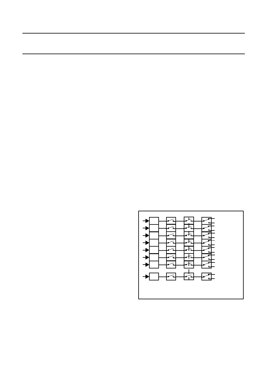
2000 Jun 22
33
Philips Semiconductors
Tentative Device Specification
TV signal processor-Teletext decoder with
embedded
µ
-Controller
TDA955X/6X/8X PS/N1 series
I/O Facility
I/O
PORTS
The IC has 13 I/O lines, each is individually addressable,
or form part of 4 parallel addressable ports which are
port0, port1, port2 and port3.
P
ORT TYPE
All individual ports can be programmed to function in one
of four modes, the mode is defined by two Port
Configuration SFRs. The modes available are Open Drain,
Quasi-bidirectional, High Impedance and Push-Pull.
Open Drain
The Open drain mode can be used for bi-directional
operation of a port. It requires an external pull-up resistor,
the pull-up voltage has a maximum value of 5.5V, to allow
connection of the device into a 5V environment.
Quasi bi-directional
The quasi-bidirectional mode is a combination of open
drain and push pull. It requires an external pull-up resistor
to VDDp (nominally 3.3V). When a signal transition from
0->1 is output from the device, the pad is put into push-pull
mode for one clock cycle (166ns) after which the pad goes
into open drain mode. This mode is used to speed up the
edges of signal transitions. This is the default mode of
operation of the pads after reset.
High Impedance
The high impedance mode can be used for Input only
operation of the port. When using this configuration the two
output transistors are turned off.
Push-Pull
The push pull mode can be used for output only. In this
mode the signal is driven to either 0V or VDDp, which is
nominally 3.3V.
Interrupt System
The device has 8 interrupt sources, each of which can be
enabled or disabled. When enabled, each interrupt can be
assigned one of two priority levels. There are four
interrupts that are common to the 80C51, two of these are
external interrupts (EX0 and EX1) and the other two are
timer interrupts (ET0 and ET1). There is also one interrupt
connected to the 80c51 micro-controller IIC peripheral for
Transmit and Receive operation.
The TDA955x/6x/8x family of devices have an additional
16-bit Timer (with 8-bit Pre-scaler). To accommodate this,
another interrupt ET2PR has been added to indicate timer
overflow.
In addition to the conventional 80c51, two application
specific interrupts are incorporated internal to the device
which have the following functionality:-
CC (Closed Caption Data Ready Interrupt) - This
interrupt is generated when the device is configured for
Closed Caption acquisition. The interrupt is activated at
the end of the currently selected Slice Line as defined in
the CCLIN SFR.
BUSY (Display Busy Interrupt) - An interrupt is
generated when the Display enters either a Horizontal or
Vertical Blanking Period. i.e. Indicates when the
micro-controller can update the Display RAM without
causing undesired effects on the screen. This interrupt can
be configured in one of two modes using the MMR
Configuration Register (Address 87FF, Bit-3 [TXT/V]):-
∑
TeXT Display Busy: An interrupt is generated on each
active horizontal display line when the Horizontal
Blanking Period is entered.
∑
Vertical Display Busy: An interrupt is generated on each
vertical display field when the Vertical Blanking Period is
entered.
I
NTERRUPT
E
NABLE
S
TRUCTURE
Each of the individual interrupts can be enabled or
disabled by setting or clearing the relevant bit in the
interrupt enable SFRs (IE and IEN1). All interrupt sources
can also be globally disabled by clearing the EA bit (IE.7).
I
NTERRUPT
E
NABLE
P
RIORITY
Each interrupt source can be assigned one of two priority
levels. The interrupt priorities are defined by the interrupt
priority SFRs (IP and IP1). A low priority interrupt can be
interrupted by a high priority interrupt, but not by another
low priority interrupt. A high priority interrupt can not be
interrupted by any other interrupt source. If two requests of
EX0
ET0
EX1
ET1
ECC
ES2
EBUSY
H1
H2
H3
H4
H5
H6
H7
L1
L2
L3
L4
L5
L6
L7
Highest Priority Level1
Highest Priority Level0
ET2PR
Lowest Priority Level1
Lowest Priority Level0
IE.0:6
IP.0:6
Source
Enable
Global
Enable
Priority
Control
IE1.0
IP1.0
IE.7
Interrupt
Source
H8
L8
Fig.10 Interrupt Structure

2000 Jun 22
34
Philips Semiconductors
Tentative Device Specification
TV signal processor-Teletext decoder with
embedded
µ
-Controller
TDA955X/6X/8X PS/N1 series
different priority level are received simultaneously, the
request with the highest priority level is serviced. If
requests of the same priority level are received
simultaneously, an internal polling sequence determines
which request is serviced. Thus, within each priority level
there is a second priority structure determined by the
polling sequence as defined in Table 4.
I
NTERRUPT
V
ECTOR
A
DDRESS
The processor acknowledges an interrupt request by
executing a hardware generated LCALL to the appropriate
servicing routine. The interrupt vector addresseses are
shown in Table 4.
L
EVEL
/E
DGE
I
NTERRUPT
The external interrupt can be programmed to be either
level-activated or transition activated by setting or clearing
the IT0/1 bits in the Timer Control SFR(TCON).
The external interrupt INT1 differs from the standard
80C51 in that it is activated on both edges when in edge
sensitive mode. This is to allow software pulse width
measurement for handling remote control inputs.
Timer/Counter
Two 16 bit timers/counters are incorporated Timer0 and
Timer1. Both can be configured to operate as either timers
or event counters.
In Timer mode, the register is incremented on every
machine cycle. It is therefore counting machine cycles.
Since the machine cycle consists of 12 oscillator periods,
the count rate is 1/12 Fosc = 1MHz.
In Counter mode, the register is incremented in response
to a negative transition at its corresponding external pin
T0/1. Since the pins T0/1 are sampled once per machine
cycle it takes two machine cycles to recognise a transition,
this gives a maximum count rate of 1/24 Fosc = 0.5MHz.
There are six special function registers used to control the
timers/counters as defined in Table 6.
Source
Priority within level
Interrupt Vector
EX0
Highest
0003H
ET0
000BH
EX1
0013H
ET1
001BH
ECC
0023H
ES2
002BH
EBUSY
0033H
ET2PR
Lowest
003BH
Table 4
Interrupt Priority (within same level)
ITx
Level
Edge
0
Active low
1
INT0 = Negative Edge
INT1 = Positive and Negative Edge
Table 5
External Interrupt Activation
SFR
Address
TCON
88H
TMOD
89H
TL0
8AH
TH0
8BH
TL1
8CH
TH1
8DH
Table 6
Timer/Counter Registers
TF1 TR TF0 TR
IE1 IT1 IE0 IT0
Symbol
Position
Name and Significance
TF1
TCON.7
Timer 1 overflow flag. Set by hard-
ware on timer/counter overflow.
Cleared by hardware when processor
vectors to interrupt routine.
TR1
TCON.6
Timer 1 Run control bit. Set/cleared
by software to turn timer.counter
on/off.
TF0
TCON.5
Timer 0 overflow flag. Set by hard-
ware on timer/counter overflow.
Cleared by hardware when processor
vectors to interrupt routine.
TR0
TCON.4
Timer 0 Run control bit. Set/cleared
by software to turn timer.counter
on/off.
Symbol
Position
Name and Significance
IE1
TCON.3
Interrupt 1 Edge flag. Set by hardware
when external interrupt edge
detected. Cleared when interrupt
processed.
IT1
TCON.2
Interrupt 1 Type control bit.
Set/cleared by software to specify fall-
ing edge/low level triggered external
interrupts.
IE0
TCON.1
Interrupt 0 Edge flag. Set by hardware
when external interrupt edge
detected. Cleared when interrupt
processed.
IT0
TCON.0
Interrupt 0 Type control bit.
Set/cleared by software to specify fall-
ing edge/low level triggered external
interrupts.
Fig.11 Timer/Counter Control (TCON) register

2000 Jun 22
35
Philips Semiconductors
Tentative Device Specification
TV signal processor-Teletext decoder with
embedded
µ
-Controller
TDA955X/6X/8X PS/N1 series
The Timer/Counter function is selected by control bits C/T
in the Timer Mode SFR (TMOD). These two
Timer/Counter have four operating modes, which are
selected by bit-pairs (M1.M0) in the TMOD. Refer to the
80C51 based 8-bit micro-controllers - Philips
Semiconductors (ref. IC20) for detail of the modes and
operation.
TL0/TL1 and TH0/TH1 are the actual timer/counter
registers for timer0 / timer1. TL0/TL1 is the low byte and
TH0/TH1 is the high byte.
T
IMER WITH
P
RE
-
SCALER
An additional 16-bit timer with 8-bit pre-scaler is provided
to allow timer periods up to 16.777 seconds. This timer
remains active during IDLE mode.
TP2L sets the lower value of the period for timer 2 and
TP2H is the upper timer value. TP2PR provides an 8-bit
pre-scaler for timer 2. The value on TP2PR, TP2H and
TP2L shall never change unless updated by the software.
If the micro reads TP2R, TP2H orTP2L at any stage, this
should return the value written and not the current timer 2
value. The timer 2 should continue after overflow by
re-loading the timer with the values of SFRs TP2PR, TP2H
and TP2L.
TP2CL and TP2CH indicate the current timer 2 value.
These should be readable both when the timer 2 is active
and inactive. Once the timer 2 is disabled, the timer 2 value
at the time of disabling should be maintained on the SFRs
TP2CL and TP2CH. At a count of zero (on TP2CL and
TP2CH), the overflow flag should be set :- TP2CRL<1> -
'0' = no timer 2 overflow, '1'= timer 2 overflow.
TP2CRL is the control and status for timer 2. TP2CRL.0 is
the timer enable and TP2CRL.1 is the timer overflow
status. The overflow flag will need to be reset by software.
Hence, if required, software may poll flag rather than use
interrupt. Upon overflow an interrupt should also be
generated.
Reset values of all registers should be 00 hex.
In Timer mode, Timer 2 should count down from the value
set on SFRs TP2PR, TP2H and TP2L. It is therefore
counting machine cycles. Since the machine cycle
consists of 12 oscillator periods, the count rate is 1/12 fosc
(1MHz).
Timer2 interval = ( TP2H * 256 + TP2L ) * ( TP2PR + 1 ) * 1 us
WatchDog Timer
The WatchDog timer is a counter that once in an overflow
state forces the micro-controller in to a reset condition. The
purpose of the WatchDog timer is to reset the
micro-controller if it enters an erroneous processor state
(possibly caused by electrical noise or RFI) within a
reasonable period of time. When enabled, the WatchDog
circuitry will generate a system reset if the user program
fails to reload the WatchDog timer within a specified length
of time known as the WatchDog interval.
The WatchDog timer consists of an 8-bit counter with an
16-bit pre-scaler. The pre-scaler is fed with a signal whose
frequency is 1/12 fosc (1MHz).
The 8 bit timer is incremented every `t' seconds where:
t=12x65536x1/fosc=12x65536x1/12x10
6
= 65.536ms
W
ATCH
D
OG
T
IMER OPERATION
The WatchDog operation is activated when the WLE bit in
the Power Control SFR (PCON) is set. The WatchDog can
be disabled by Software by loading the value 55H into the
WatchDog Key SFR (WDTKEY). This must be performed
before entering Idle/Power Down mode to prevent exiting
the mode prematurely.
Once activated the WatchDog timer SFR (WDT) must be
reloaded before the timer overflows. The WLE bit must be
set to enable loading of the WDT SFR, once loaded the
WLE bit is reset by hardware, this is to prevent erroneous
Software from loading the WDT SFR.
The value loaded into the WDT defines the WatchDog
interval.
WatchDog interval = (256 - WDT) * t = (256 -WDT) * 65.536ms.
The range of intervals is from WDT=00H which gives
16.777s to WDT=FFH which gives 65.536ms.
PORT Alternate Functions
The Ports 1,2 and 3 are shared with alternate functions to
enable control of external devices and circuitry. The
alternate functions are enabled by setting the appropriate
Gat C/T M1
M0 Gat C/T M1
M0
Timer 1
Timer 0
Gate
Gating control when set. Timer/counter is enabled only
while px_int_n is high and TR control bit is set. When
cleared timer/counter is enabled whenever TR control bit
is set.
C/T
Timer or Counter selector. Cleared for timer operation
(input from system clock). Set for counter operation (input
from T input pin.
M1
M0
Operating
0
0
8048 Timer, TL serves as 5-bit prescaler.
0
1
16-bit Timer/Counter, TL and TH are cascaded.
1
0
8-bit auto-reload Timer/Counter, TH holds a value
which is to be loaded into TL.
1
1
timer 0: two 8-bit Timers/Counters. TL0 is controlled by
timer 0 control bits. TH0 is controlled by timer 1 control
bits. timer 1: stopped.
Fig.12 Timer/Counter Mode control (TMOD)

2000 Jun 22
36
Philips Semiconductors
Tentative Device Specification
TV signal processor-Teletext decoder with
embedded
µ
-Controller
TDA955X/6X/8X PS/N1 series
SFR and also writing a `1' to the Port bit that the function
occupies.
PWM P
ULSE
W
IDTH
M
ODULATORS
The device has four 6-bit Pulse Width Modulated (PWM)
outputs for analogue control of e.g. volume, balance, bass,
treble, brightness, contrast, hue and saturation. The PWM
outputs generate pulse patterns with a repetition rate of
21.33us, with the high time equal to the PWM SFR value
multiplied by 0.33us. The analogue value is determined by
the ratio of the high time to the repetition time, a D.C.
voltage proportional to the PWM setting is obtained by
means of an external integration network (low pass filter).
PWM Control
The relevant PWM is enabled by setting the PWM enable
bit PWxE in the PWMx Control register. The high time is
defined by the value PWxV<5:0>
TPWM T
UNING
P
ULSE
W
IDTH
M
ODULATOR
The device has a single 14-bit PWM that can be used for
Voltage Synthesis Tuning. The method of operation is
similar to the normal PWM except the repetition period is
42.66us.
TPWM Control
Two SFRs are used to control the TPWM, they are TDACL
and TDACH. The TPWM is enabled by setting the TPWE
bit in the TDACH SFR. The most significant bits TD<13:7>
alter the high period between 0 and 42.33us. The 7 least
significant bits TD<6:0> extend certain pulses by a further
0.33us. e.g. if TD<6:0> = 01H then 1 in 128 periods will be
extended by 0.33us, if TD<6:0>=02H then 2 in 128 periods
will be extended.
The TPWM will not start to output a new value until TDACH
has been written to. Therefore, if the value is to be
changed, TACL should be written before TDACH.
SAD S
OFTWARE
A/D
Four successive approximation Analogue to Digital
Converters can be implemented in software by making use
of the on board 8-bit Digital to Analogue Converter and
Analogue Comparator.
SAD Control
The control of the required analogue input is done using
the channel select bits CH<1:0> in the SAD SFR, this
selects the required analogue input to be passed to one of
the inputs of the comparator. The second comparator input
is generated by the DAC whose value is set by the bits
SAD<7:0> in the SAD and SADB SFRs. A comparison
between the two inputs is made when the start compare bit
ST in the SAD SFR is set, this must be at least one
instruction cycle after the SAD<7:0> value has been set.
The result of the comparison is given on VHI one
instruction cycle after the setting of ST.
SAD Input Voltage
The external analogue voltage that is used for comparison
with the internally generated DAC voltage does not have
the same voltage range. The DAC has a lower reference
level of V
SSA
and an upper reference level of V
SSA
. The
resolution of the DAC voltage with a nominal value is
3.3/256 ~ 13mV. The external analogue voltage has a
lower value equivalent to V
SSA
and an upper value
equivalent to V
DDP
- V
tn
, were V
tn
is the threshold voltage
for an NMOS transistor. The reason for this is that the input
pins for the analogue signals (P3.0 to P3.3) are 5V tolerant
for normal port operations, i.e. when not used as analogue
input. To protect the analogue multiplexer and comparator
circuitry from the 5V, a series transistor is used to limit the
voltage. This limiting introduces a voltage drop equivalent
to V
tn
(~0.6V) on the input voltage. Therefore, for an input
voltage in the range V
DDP
to V
DDp
-V
tn
the SAD returns the
same comparison value.
SAD DC Comparator Mode
The SAD module incorporates a DC Comparator mode
which is selected using the 'DC_COMP' control bit in the
SADB SFR. This mode enables the micro-controller to
detect a threshold crossing at the input to the selected
analogue input pin (P3.0, P3.1, P3.2 or P3.3) of the
Software A/D Converter. A level sensitive interrupt is
generated when the analogue input voltage level at the pin
falls below the analogue output level of the SAD D/A
converter.
This mode is intended to provide the device with a
wake-up mechanism from Power-Down or Idle when a
key-press on the front panel of the TV is detected.
+
-
VHI
MUX
4-1
8-bit
DAC
SAD<7:0>
ADC0
ADC1
ADC2
ADC3
CH<1:0>
V
DDP
Fig.13 SAD Block Diagram
2000 Jun 22
37
Philips Semiconductors
Tentative Device Specification
TV signal processor-Teletext decoder with
embedded
µ
-Controller
TDA955X/6X/8X PS/N1 series
The following software sequence should be used when
utilizing this mode for Power-Down or Idle:-
1. Disable INT1 using the IE SFR.
2. Set INT1 to level sensitive using the TCON SFR.
3. Set the D/A Converter digital input level to the desired
threshold level using the SAD/SADB SFRs and select
the required input pin (P3.0, P3.1, P3.2 or P3,3) using
CH1, CH0 in the SAD SFR.
4. Enter DC Compare mode by setting the 'DC_COMP'
enable bit in the SADB SFR.
5. Enable INT1 using the IE SFR.
6. Enter Power-Down/Idle. Upon wake-up the SAD
should be restored to its conventional operating mode
by disabling the 'DC_COMP' control bit.
I2C Serial I/O Bus
The I
2
C bus consists of a serial data line (SDA) and a serial
clock line (SCL). The definition of the I
2
C protocol can be
found in the 80C51 based 8-bit micro-controllers - Philips
Semiconductors (ref. IC20).
The device operates in four modes: -
∑
Master Transmitter
∑
Master Receiver
∑
Slave Transmitter
∑
Slave Receiver
The micro-controller peripheral is controlled by the Serial
Control SFR (S1CON) and its Status is indicated by the
status SFR (S1STA). Information is transmitted/received
to/from the I
2
C bus using the Data SFR (S1DAT) and the
Slave Address SFR (S1ADR) is used to configure the
slave address of the peripheral.
The byte level I
2
C serial port is identical to the I
2
C serial
port on the 8xC558, except for the clock rate selection bits
CR<2:0>. The operation of the subsystem is described in
detail in the 8xC558 datasheet and can be found in the
80C51 based 8-bit micro-controllers - Philips
Semiconductors (ref. IC20).
Three different IIC selection tables for CR<2:0> can be
configured using the ROMBANK SFR (IIC_LUT<1:0>) as
follows: -
`558 nominal mode' (iic_lut="00")
This option accommodates the 558 I2C. The various serial
rates are shown below: -
`558 fast mode' (iic_lut="01")
This option accommodates the 558 I
2
C doubled rates as
shown below: -
`558 slow mode' (iic_lut="10")
This option accommodates the 558 I
2
C rates divided by 2
as shown below: -
CR2
CR1
CR0
f
clk
(6MHz)
divided by
I2C Bit Frequency
(KHz) at f
clk
0
0
0
60
100
0
0
1
1600
3.75
0
1
0
40
150
0
1
1
30
200
1
0
0
240
25
1
0
1
3200
1.875
1
1
0
160
37.5
1
1
1
120
50
Table 7
IIC Serial Rates `558 nominal mode'
CR2
CR1
CR0
f
clk
(6MHz)
divided by
I2C Bit Frequency
(KHz) at f
clk
0
0
0
30
200
0
0
1
800
7.5
0
1
0
20
300
0
1
1
15
400
1
0
0
120
50
1
0
1
1600
3.75
1
1
0
80
75
1
1
1
60
100
Table 8
IIC Serial Rates `558 fast mode'
CR2
CR1
CR0
f
clk
(6MHz)
divided by
I2C Bit Frequency
(KHz) at f
clk
0
0
0
120
50
0
0
1
3200
1.875
0
1
0
80
75
0
1
1
60
100
1
0
0
480
12.5
1
0
1
6400
0.9375
Table 9
IIC Serial Rates `558 slow mode'

2000 Jun 22
38
Philips Semiconductors
Tentative Device Specification
TV signal processor-Teletext decoder with
embedded
µ
-Controller
TDA955X/6X/8X PS/N1 series
Note: In the above tables the f
clk
relates to the clock rate of
the 80c51 IIC module (6MHz).
I2C Port Enable
One external I
2
C port is available. This port is enabled
using TXT21.I2C PORT0. Any information transmitted to
the device can only be acted upon if the port is enabled.
Internal communication between the 80c51
micro-controller and the TV Signal Processor will continue
regardless of the value written to TXT21.I2C PORT0.
LED Support
Port pins P0.5 and P0.6 have a 8mA current sinking
capability to enable LEDs in series with current limiting
resistors to be driven directly, without the need for
additional buffering circuitry.
MEMORY INTERFACE
The memory interface controls the access to the
embedded DRAM, refreshing of the DRAM and page
clearing. The DRAM is shared between Data Capture,
Display and Microcontroller sections. The Data Capture
section uses the DRAM to store acquired information that
has been requested. The Display reads the DRAM
information and converts it to RGB output values. The
Microcontroller uses the DRAM as embedded auxiliary
RAM.
DATA CAPTURE
The Data Capture section takes in the analogue
Composite Video and Blanking Signal (CVBS) from One
Chip, and from this extracts the required data, which is
then decoded and stored in SFR memory.
The extraction of the data is performed in the digital
domain. The first stage is to convert the analogue CVBS
signal into a digital form. This is done using an ADC
sampling at 12MHz. The data and clock recovery is then
performed by a Multi-Rate Video Input Processor
(MulVIP). From the recovered data and clock the following
data types are extracted WST Teletext (625/525),Closed
Caption, VPS, WSS. The extracted data is stored in either
memory (DRAM) via the Memory Interface or in SFR
locations.
Data Capture Features
∑
Video Signal Quality detector.
∑
Data Capture for 625 line WST
∑
Data Capture for 525 line WST
∑
Data Capture for US Closed Caption
∑
Data Capture for VPS data (PDC system A)
∑
Data Capture for Wide Screen Signalling (WSS) bit
decoding
∑
Automatic selection between 525 WST/625WST
∑
Automatic selection between 625WST/VPS on line 16 of
VBI
∑
Real-time capture and decoding for WST Teletext in
Hardware, to enable optimised microprocessor
throughput
∑
Upto 10 pages stored On-Chip
∑
Inventory of transmitted Teletext pages stored in the
Transmitted Page Table (TPT) and Subtitle Page Table
(SPT)
∑
Automatic detection of FASTEXT transmission
∑
Real-time packet 26 engine in Hardware for processing
accented, G2 and G3 characters
∑
Signal quality detector for WST/VPS data types
∑
Comprehensive Teletext language coverage
∑
Full Field and Vertical Blanking Interval (VBI) data
capture of WST data
Analogue to Digital Converter
The CVBS input is passed through a differential to single
ended converter (DIVIS), although in this device it is used
in single ended configuration with a reference.The
analogue output of DIVIS is converted into a digital
representation by a full flash ADC with a sampling rate of
12MHz.
Multi Rate Video Input Processor
The multi rate video input processor is a Digital Signal
Processor designed to extract the data and recover the
clock from the digital CVBS signal.
1
1
0
320
18.75
1
1
1
240
25
CR2
CR1
CR0
f
clk
(6MHz)
divided by
I2C Bit Frequency
(KHz) at f
clk
Table 9
IIC Serial Rates `558 slow mode'

2000 Jun 22
39
Philips Semiconductors
Tentative Device Specification
TV signal processor-Teletext decoder with
embedded
µ
-Controller
TDA955X/6X/8X PS/N1 series
Data Standards
The data and clock standards that can be recovered are
shown in Table 10 below:-
Data Capture Timing
The Data Capture timing section uses the Synchronisation
information extracted from the CVBS signal to generate
the required Horizontal and Vertical reference timings.
The timing section automatically recognises and selects
the appropriate timings for either 625 (50Hz)
synchronisation or 525 (60Hz) synchronisation. A flag
TXT12.Video Signal Quality is set when the timing section
is locked correctly to the incoming CVBS signal. When
TXT12.Video Signal Quality is set another flag
TXT12.625/525 SYNC can be used to identify the
standard.
Acquisition
The acquisition sections extracts the relevant information
from the serial stream of data from the MulVIP and stores
it in memory.
625 WST A
CQUISITION
The family is capable of acquiring 625-line and 525-line
World System Teletext. Teletext pages are identified by
seven numbers: magazine (page hundreds), page tens,
page units, hours tens, hours units, minutes tens and
minutes units. The last four digits, hours and minutes, are
known as the subcode, and were originally intended to be
time related, hence their names.
Making a page request
A page is requested by writing a series of bytes into the
TXT3.PRD<4:0> SFR which correspond to the number of
the page required. The bytes written into TXT3 are stored
in a RAM with an auto-incrementing address. The start
address for the RAM is set using the TXT2.SC<2:0> to
define which part of the page request is being written, and
TXT2.REQ<3:0> is used to define which of the 10 page
requests is being modified. If TXT2.REQ<3:0> is greater
than 09h, then data being written to TXT3 is ignored. Table
11 shows the contents of the page request RAM.
Up to 10 pages of teletext can be acquired on the 10 page
device, when TXT1.EXT PKT OFF is set to logic 1, and up
to 9 pages can be acquired when this bit is set to logic 0.
f the 'Do Care' bit for part of the page number is set to 0
then that part of the page number is ignored when the
teletext decoder is deciding whether a page being
received off air should be stored or not. For example, if the
Do Care bits for the 4 subcode digits are all set to 0 then
every subcode version of the page will be captured.
Table 11 The contents of the Page request RAM
Note: MAG = Magazine PT = Page Tens PU = Page Units
HT = Hours Tens HU = Hours Units
MT = Minutes Tens MU = Minutes Units E = Error check
mode
When the Hold bit is set to 0 the teletext decoder will not
recognise any page as having the correct page number
and no pages will be captured. In addition to providing the
user requested hold function this bit should be used to
prevent the inadvertent capture of an unwanted page
when a new page request is being made. For example, if
the previous page request was for page 100 and this was
being changed to page 234, it would be possible to capture
page 200 if this arrived after only the requested magazine
number had been changed.
The E1 and E0 bits control the error checking which should
be carried out on packets 1 to 23 when the page being
requested is captured. This is described in more detail in a
later section (`Error Checking').
For a multi page device, each packet can only be written
into one place in the teletext RAM so if a page matches
more than one of the page requests the data is written into
the area of memory corresponding to the lowest numbered
matching page request.
At power-up each page request defaults to any page, hold
on and error check mode 0.
Rolling Headers and Time
When a new page has been requested it is conventional
for the decoder to turn the header row of the display green
Data Standard
Clock Rate
625WST
6.9375 MHz
525WST
5.7272 MHz
VPS
5.0 MHz
WSS
5.0 MHz
Closed Caption
500 KHz
Table 10 Data Slicing Standards
Start
Column
Byte
Identification
PRD<4>
PRD<3>
PRD<2>
PRD<1>
PRD<0>
0
Magazine
DO CARE
HOLD
MAG2
MAG1
MAG0
1
Page Tens
DO CARE
PT3
PT2
PT1
PT0
2
Page Units
DO CARE
PU3
PU2
PU1
PU0
3
Hours Tens
DO CARE
x
x
HT1
HT0
4
Hours Units
DO CARE
HU3
HU2
HU1
HU0
5
Minutes Tens
DO CARE
x
MT2
MT1
MT0
6
Minutes Units
DO CARE
MU3
MU2
MU1
MU0
7
Error Mode
x
x
x
E1
E0

2000 Jun 22
40
Philips Semiconductors
Tentative Device Specification
TV signal processor-Teletext decoder with
embedded
µ
-Controller
TDA955X/6X/8X PS/N1 series
and to display each page header as it arrives until the
correct page has been found.
When a page request is changed (i.e.: when the TXT3
SFR is written to) a flag (PBLF) is written into bit 5, column
9, row 25 of the corresponding block of the page memory.
The state of the flag for each block is updated every TV
line, if it is set for the current display block, the acquisition
section writes all valid page headers which arrive into the
display block and automatically writes an alpha-numerics
green character into column 7 of row 0 of the display block
every TV line.
When a requested page header is acquired for the first
time, rows 1 to 23 of the relevant memory block are
cleared to space, i.e.: have 20h written into every column,
before the rest of the page arrives. Row 24 is also cleared
if the TXT0.X24 POSN bit is set. If the TXT1.EXT PKT OFF
bit is set the extension packets corresponding to the page
are also cleared.
The last 8 characters of the page header are used to
provide a time display and are always extracted from every
valid page header as it arrives and written into the display
block
The TXT0. DISABLE HEADER ROLL bit prevents any
data being written into row 0 of the page memory except
when a page is acquired off air i.e.: rolling headers and
time are not written into the memory. The TXT1.ACQ OFF
bit prevents any data being written into the memory by the
teletext acquisition section.
When a parallel magazine mode transmission is being
received only headers in the magazine of the page
requested are considered valid for the purposes of rolling
headers and time. Only one magazine is used even if don't
care magazine is requested. When a serial magazine
mode transmission is being received all page headers are
considered to be valid.
Error Checking
Before teletext packets are written into the page memory
they are error checked. The error checking carried out
depends on the packet number, the byte number, the error
check mode bits in the page request data and the TXT1.8
BIT bit.
If an incorrectable error occurs in one of the Hamming
checked addressing and control bytes in the page header
or in the Hamming checked bytes in packet 8/30, bit 4 of
the byte written into the memory is set, to act as an error
flag to the software. If incorrectable errors are detected in
any other Hamming checked data the byte is not written
into the memory.
Teletext Memory Organisation
The teletext memory is divided into 2 banks of 10 blocks.
Normally, when the TXT1.EXT PKT OFF bit is logic 0,
each of blocks 0 to 8 contains a teletext page arranged in
the same way as the basic page memory of the page
device and block 9 contains extension packets. When the
TXT1.EXT PKT OFF bit is logic 1, no extension packets
are captured and block 9 of the memory is used to store
another page. The number of the memory block into which
a page is written corresponds to the page request number
which resulted in the capture of the page.
Packet 0, the page header, is split into 2 parts when it is
written into the text memory. The first 8 bytes of the header
contain control and addressing information. They are
Hamming decoded and written into columns 0 to 7 of row
25. Row 25 also contains the magazine number of the
acquired page and the PBLF flag but the last 14 bytes are
unused and may be used by the software, if necessary.
Row 25 Data Contents
The Hamming error flags are set if the on-board 8/4
Hamming checker detects that there has been an
incorrectable (2 bit) error in the associated byte. It is
possible for the page to still be acquired if some of the
page address information contains incorrectable errors if
that part of the page request was a 'don't care'. There is no
error flag for the magazine number as an incorrectable
error in this information prevents the page being acquired.
The interrupted sequence (C9) bit is automatically dealt
with by the acquisition section so that rolling headers do
not contain a discontinuity in the page number sequence.
The magazine serial (C11) bit indicates whether the
transmission is a serial or a parallel magazine
transmission. This affects the way the acquisition section
operates and is dealt with automatically.
The newsflash (C5), subtitle (C6), suppress header (C7),
inhibit display (C10) and language control (C12 to 14) bits
are dealt with automatically by the display section,
described below.
The update (C8) bit has no effect on the hardware. The
remaining 32 bytes of the page header are parity checked
and written into columns 8 to 39 of row 0. Bytes which pass
the parity check have the MSB set to 0 and are written into
the page memory. Bytes with parity errors are not written
into the memory.
Inventory Page
If the TXT0.INV on bit is 1, memory block 8 is used as an
inventory page. The inventory page consists of two tables,
- the Transmitted Page Table (TPT) and the subtitle page
table (SPT).
In each table, every possible combination of the page tens
and units digit, 00 to FFh, is represented by a byte. Each
bit of these bytes corresponds to a magazine number so
each page number, from 100 to 8FF, is represented by a
bit in the table.The bit for a particular page in the TPT is set

2000 Jun 22
41
Philips Semiconductors
Tentative Device Specification
TV signal processor-Teletext decoder with
embedded
µ
-Controller
TDA955X/6X/8X PS/N1 series
when a page header is received for that page. The bit in
the SPT is set when a page header for the page is received
which has the `subtitle' page header control bit (C6)
set.The bit for a particular page in the TPT is set when a
page header is received for that page. The bit in the SPT
is set when a page header for the page is received which
has the `subtitle' page header control bit (C6) set.
Packet 26 Processing
One of the uses of packet 26 is to transmit characters
which are not in the basic teletext character set. The family
automatically decodes packet 26 data and, if a character
corresponding to that being transmitted is available in the
character set, automatically writes the appropriate
character code into the correct location in the teletext
memory. This is not a full implementation of the packet 26
specification allowed for in level 2 teletext, and so is often
referred to as level 1.5.
By convention, the packets 26 for a page are transmitted
before the normal packets. To prevent the default
character data over writing the packet 26 data the device
incorporates a mechanism which prevents packet 26 data
from being overwritten. This mechanism is disabled when
the Spanish national option is detected as the Spanish
transmission system sends even parity (i.e. incorrect)
characters in the basic page locations corresponding to
the characters sent via packet 26 and these will not over
write the packet 26 characters anyway. The special
treatment of Spanish national option is prevented if
TXT12. ROM VER R4 is logic 0 or if the TXT8.DISABLE
SPANISH is set.
Packet 26 data is processed regardless of the TXT1. EXT
PKT OFF bit, but setting theTXT1.X26 OFF disables
packet 26 processing.
The TXT8. Packet 26 received bit is set by the hardware
whenever a character is written into the page memory by
the packet 26 decoding hardware. The flag can be reset by
writing a 0 into the SFR bit.
525 WST
The 525 line format is similar to the 625 line format but the
data rate is lower and there are less data bytes per packet
(32 rather than 40). There are still 40 characters per
display row so extra packets are sent each of which
contains the last 8 characters for four rows. These packets
can be identified by looking at the `tabulation bit' (T), which
replaces one of the magazine bits in 525 line teletext.
When an ordinary packet with T = 1 is received, the
decoder puts the data into the four rows starting with that
corresponding to the packet number, but with the 2 LSBs
set to 0. For example, a packet 9 with T = 1 (packet X/1/9)
contains data for rows 8, 9, 10 and 11. The error checking
carried out on data from packets with T = 1 depends on the
setting of the TXT1. 8 BIT bit and the error checking control
bits in the page request data and is the same as that
applied to the data written into the same memory location
in the 625 line format.
The rolling time display (the last 8 characters in row 0) is
taken from any packets X/1/1, 2 or 3 received. In parallel
magazine mode only packets in the correct magazine are
used for rolling time. Packet number X/1/0 is ignored.
The tabulation bit is also used with extension packets. The
first 8 data bytes of packet X/1/24 are used to extend the
Fastext prompt row to 40 characters. These characters are
written into whichever part of the memory the packet 24 is
being written into (determined by the `X24 Posn' bit).
Packets X/0/27/0 contain 5 Fastext page links and the link
control byte and are captured, Hamming checked and
stored by in the same way as are packets X/27/0 in 625
line text. Packets X/1/27/0 are not captured.
Because there are only 2 magazine bits in 525 line text,
packets with the magazine bits all set to 0 are referred to
as being in magazine 4. Therefore, the broadcast service
data packet is packet 4/30, rather than packet 8/30. As in
625 line text, the first 20 bytes of packet 4/30 contain
encoded data which is decoded in the same way as that in
packet 8/30. The last 12 bytes of the packet contains half
of the parity encoded status message. Packet 4/0/30
contains the first half of the message and packet 4/1/30
contains the second half. The last 4 bytes of the message
are not written into memory. The first 20 bytes of the each
version of the packet are the same so they are stored
whenever either version of the packet is acquired.
In 525 line text each packet 26 only contains ten 24/18
Hamming encoded data triplets, rather than the 13 found
in 625 line text. The tabulation bit is used as an extra bit
(the MSB) of the designation code, allowing 32 packet 26s
to be transmitted for each page. The last byte of each
packet 26 is ignored.
F
ASTEXT
D
ETECTION
When a packet 27, designation code 0 is detected,
whether or not it is acquired, the TXT13. FASTEXT bit is
set. If the device is receiving 525 line teletext, a packet
X/0/27/0 is required to set the flag. The flag can be reset
by writing a 0 into the SFR bit.
B
ROADCAST
S
ERVICE
D
ATA
D
ETECTION
When a packet 8/30 is detected, or a packet 4/30 when the
device is receiving a 525 line transmission, the TXT13.
Packet 8/30. The flag can be reset by writing a 0 into the
SFR bit.
VPS A
CQUISITION
When the TXT0. VPS ON bit is set, any VPS data present
on line 16, field 0 of the CVBS signal at the input of the

2000 Jun 22
42
Philips Semiconductors
Tentative Device Specification
TV signal processor-Teletext decoder with
embedded
µ
-Controller
TDA955X/6X/8X PS/N1 series
teletext decoder is error checked and stored in row 25,
block 9 of the basic page memory. The device
automatically detects whether teletext or VPS is being
transmitted on this line and decodes the data
appropriately.
Each VPS byte in the memory consists of 4 bi-phase
decoded data bits (bits 0-3), a bi-phase error flag (bit 4)
and three 0s (bits5-7). The TXT13. VPS Received bit is set
by the hardware whenever VPS data is acquired. The flag
can be reset by writing a 0 into the SFR bit.
WSS A
CQUISITION
The Wide Screen Signalling data transmitted on line 23
gives information on the aspect ratio and display position
of the transmitted picture, the position of subtitles and on
the camera/film mode. Some additional bits are reserved
for future use. A total of 14 data bits are transmitted. All of
the available data bits transmitted by the Wide Screen
Signalling signal are captured and stored in SFRs WSS1,
WSS2 and WSS3. The bits are stored as groups of related
bits and an error flag is provided for each group to indicate
when a transmission error has been detected in one or
more of the bits in the group. Wide screen signalling data
is only acquired when the TXT8.WSS ON bit is set. The
TXT8.WSS RECEIVED bit is set by the hardware
whenever wide screen signalling data is acquired. The flag
can be reset by writing a 0 into the SFR bit.
C
LOSED
C
APTION
A
CQUISITION
The US Closed Caption data is transmitted on line 21 (525
line timings) and is used for Captioning information, Text
information and Extended Data Services. Closed Caption
data is only acquired when TXT21.CC ON bit is set.
Two bytes of data are stored per field in SFRs, the first bye
is stored in CCDAT1 and the second byte is stored in
CCDAT2. The value in the CCDAT registers are reset to
00h at the start of the Closed Caption line defined by
CCLIN.CS<4:0>. At the end of the Closed Caption line an
interrupt is generated if IE.ECC is active.
The processing of the Closed Caption data to convert into
a displayable format is performed by Software.
DISPLAY
The display section is based on the requirements for a
Level 1.5 WST Teletext and US Closed Caption. There are
some enhancements for use with locally generated
On-Screen Displays.
The display section reads the contents of the Display
memory and interprets the control/character codes. Using
this information and other global settings, the display
produces the required RGB signals and Video/Data (Fast
Blanking) signal for the TV signal processing.
The display is synchronised to the TV signal processing by
way of Horizontal and Vertical sync signals generated
within TDA955x/6x/8x. From these signals all display
timings are derived.
Display Features
∑
Teletext and Enhanced OSD modes
∑
Level 1.5 WST features
∑
US Closed Caption Features
∑
Serial and Parallel Display Attributes
∑
Single/Double/Quadruple Width and Height for
characters
∑
Scrolling of display region.
∑
Variable flash rate controlled by software.
∑
Globally selectable scan lines per row 9/10/13/16.
∑
Globally selectable character matrix (HxV) 12x9, 12x10,
12x13, 12x16.
∑
Italics, Underline and Overline.
∑
Soft Colours using CLUT with 4096 colour palette.
∑
Fringing (Shadow) selectable from N-S-E-W direction.
∑
Fringe colour selectable.
∑
Meshing of defined area.
∑
Contrast reduction of defined area.
∑
Cursor.
∑
Special Graphics characters with two planes, allowing
four colours per character.
∑
32 Software re-definable On-Screen Display characters.
∑
4 WST Character sets(G0/G2) in single device (e.g.
Latin,Cyrillic,Greek,Arabic).
∑
G1 Mosaic graphics, Limited G3 Line drawing
characters.
∑
WST Character sets and Closed Caption Character set
in single device.
Display Modes
The display section has two distinct modes with different
features available in each. The two modes are:
Fig.14 VPS Data Storage
Teletext page
header data
VPS
byte 11
VPS
byte 12
VPS
byte 13
VPS
byte 14
VPS
byte 15
VPS
byte 4
VPS
byte 5
0
9 10
11
12
13
14
15 16 17
18
19 20 21
22 23
column
row 25

2000 Jun 22
43
Philips Semiconductors
Tentative Device Specification
TV signal processor-Teletext decoder with
embedded
µ
-Controller
TDA955X/6X/8X PS/N1 series
∑
TXT:This is the display configured as the WST mode
with additional serial and global attributes to enable
the same functionality as the SAA5497 (ETT)
device.The display is configured as a fixed 25 rows
with 40 characters per row.
∑
CC:This is the display configured as the US Closed
Caption mode with the same functionality as the
PC83C771 device. The display is configured as a
maximum of 16 rows with a maximum of 48
characters per row.
In both of the above modes the Character matrix, and TV
lines per row can be defined. There is an option of 9, 10,
13 & 16 TV lines per display row, and a Character matrix
(HxV) of 12x9, 12x10, 12x13, or 12x16. Not all
combinations of TV lines per row and maximum display
rows give a sensible OSD display, since there is limited
number of TV scan lines available.
Special Function Register, TXT21 is used to control the
character matrix and lines per row.
Display Features available in each mode
The following is a list of features available in each mode.
Each setting can either be a serial or parallel attribute, and
some have a global effect on the display.
Feature
TXT
CC
Flash
serial
serial
Boxes
Txt/OSD (Serial)
serial
Horizontal Size
x1/x2/x4 (serial)
x1/x2 (serial)
Vertical Size
x1/x2 (serial)
x4 (global)
x1/x2 (serial)
Italic
N/A
serial
Foreground
colours
8 (serial)
8+8 (parallel)
Background
colours
8 (serial)
16 (serial)
Soft Colours
(CLUT)
16 from 4096
16 from 4096
Underline
N/A
serial
Overline
N/A
serial
Fringe
N+S+E+W
N+S+E+W
Fringe Colour
16 (Global)
16 (Serial)
Meshing of
Background
Black or Colour
(Global)
All (Global)
Fast Blanking
Polarity
YES
YES
Screen Colour
16 (Global)
16 (Global)
DRCS
32 (Global)
32 (Global)
Character Matrix
(HxV)
12x9/10/13/16
12x9/10/13/16
No. of Rows
25
16
No. of Columns
40
48
No of Characters
displayable
1000
768
Cursor
YES
YES
Special Graphics
(2 planes per
character)
16
16
Scroll
NO
YES
Table 12 Display Features

2000 Jun 22
44
Philips Semiconductors
Tentative Device Specification
TV signal processor-Teletext decoder with
embedded
µ
-Controller
TDA955X/6X/8X PS/N1 series
Display Feature Descriptions
F
LASH
Flashing causes the foreground colour pixel to be
displayed as the background pixels.The flash frequency is
controlled by software setting and resetting display
register REG0: Status at the appropriate interval.
CC: This attribute is valid from the time set (see Table 18)
until the end of the row or until otherwise modified.
TXT: This attribute is set by the control character `flash'
(08h) and remains valid until the end of the row or until
reset by the control character `steady' (09h).
B
OXES
CC: This attribute is valid from the time set until end of row
or otherwise modified if set with Serial Mode 0. If set with
Serial Mode 1, then it is set from the next character
onwards.
In CC text mode the background colour is displayed
regardless of the setting of the box attribute bit. Boxes take
affect only during mixed mode, where boxes are set in this
mode the background colour is displayed. Character
locations where boxes are not set show video/screen
colour (depending on the setting in the display control
register. REG0: Display Control) in stead of the
background colour.
TXT: Two types of boxes exist the Teletext box and the
OSD box. The Teletext box is activated by the `start box'
control character (0Bh), Two start box characters are
required begin a Teletext box, with box starting between
the 2 characters. The box ends at the end of the line or
after a `end box' control character.
TXT mode can also use OSD boxes, they are started using
size implying OSD control chracters(BCh/BDh/BEh/BFh).
The box starts after the control character (`set after') and
ends either at the end of the row or at the next size
implying OSD character (`set at'). The attributes flash,
teletext box, conceal, separate graphics, twist and hold
graphics are all reset at the start of an OSD box, as they
are at the start of the row. OSD Boxes are only valid in TV
mode which is defined by TXT5=03h and TXT6=03h.
S
IZE
The size of the characters can be modified in both the
horizontal and vertical directions.
CC: Two sizes are available in both the horizontal and
vertical directions. The sizes available are normal (x1),
double (x2) height/width and any combination of these.
The attribute setting is always valid for the whole row.
Mixing of sizes within a row is not possible.
TXT: Three horizontal sizes are available
normal(x1),double(x2),quadruple(x4). The control
characters `normal size' (0Ch/BCh) enables normal size,
the `double width' or double size (0Eh/BEh/0Fh/BFh)
enables double width characters. Any two consecutive
combination of `double width' or `double size'
(0Eh/BEh/0Fh/Bfh) activates quadruple width characters,
provided quadruple width characters are enabled by
TXT4.Quad Width Enable. Three vertical sizes are
available normal(x1),double(x2),quadruple(x4). The
control characters `normal size' (0Ch/BCh) enable normal
size, the `double height' or `double size'
(0Dh/BDh/0Fh/BFh) enable double height characters.
Quadruple height character are achieved by using double
height characters and setting the global attributes
TXT7.Double Height(expand) and TXT7.Bottom/Top.
If double height characters are used in teletext mode,
single height characters in the lower row of the double
height character are automatically disabled.
I
TALIC
CC: This attribute is valid from the time set until the end of
the row or otherwise modified. The attribute causes the
character foreground pixels to be offset horizontally by 1
pixel per 4 scan lines (interlaced mode). The base is the
bottom left character matrix pixel. The pattern of the
character is indented as shown in Fig.15.
2000 Jun 22
45
Philips Semiconductors
Tentative Device Specification
TV signal processor-Teletext decoder with
embedded
µ
-Controller
TDA955X/6X/8X PS/N1 series
TXT: The Italic attribute is not available.
C
OLOURS
CLUT (Colour Look Up Table)
A CLUT (Colour Look Up Table) with 16 colour entries is
provided. The colours are programmable out of a palette
of 4096(4 bits per R, G and B). The CLUT is defined by
writing data to a RAM that resides in the MOVX address
space of the 80C51.
Foreground Colour
CC: The foreground colour can be chosen from 8 colours
on a character by character basis. Two sets of 8 colours
are provided. A serial attribute switches between the
banks (see Table 18 Serial Mode 1, bit 7). The colours are
the CLUT entries 0 to 7 or 8 to 15.
TXT: The foreground colour is selected via a control
character. The colour control characters takes effect at the
start of the next character ("Set-After") and remain valid
until the end of the row, or until modified by a control
character. Only 8 foreground colours are available.
The TEXT foreground control characters map to the CLUT
entries as shown below:
Background Colour
CC: This attribute is valid from the time set until end of row
or otherwise modified if set with Serial Mode 0. If set with
Serial Mode 1, then the colour is set from the next
character onwards.
The background colour can be chosen from all 16 CLUT
entries.
0 2 4 6 8 10
Indented by 6/5/3
Indented by 5/4/2
Indented by 4/3/1
Indented by 3/2/0
Indented by 2/1
Indented by 1/0
Indented by 0
0 2 4 6 8 10 0 2 4 6 8 10 0 2 4 6 8 10 0 2 4 6 8 10 0 2 4 6 8 10
Indented by 7/6/4
0
1
2
3
4
5
6
7
8
9
10
11
12
13
14
15
Field 1
Field 2
12x16 character matrix
12x13 character matrix
12x10 character matrix
Fig.15 Italic Characters (12x10, 12x13 & 12x16).
RED3-0
b11. . .b4
GRN3-0
b7. . .b4
BLU3-0
b3. . .b0
Colour
entry
0 0 0 0
0 0 0 0
0 0 0 0
0
0 0 0 0
0 0 0 0
1 1 1 1
1
...
...
...
...
1 1 1 1
1 1 1 1
0 0 0 0
14
1 1 1 1
1 1 1 1
1 1 1 1
15
Table 13 CLUT Colour values
Control Code
Defined Colour
CLUT Entry
00h
Black
0
01h
Red
1
02h
Green
2
03h
Yellow
3
04h
Blue
4
05h
Magenta
5
06h
Cyan
6
07h
White
7
Table 14 Foreground CLUT mapping
2000 Jun 22
46
Philips Semiconductors
Tentative Device Specification
TV signal processor-Teletext decoder with
embedded
µ
-Controller
TDA955X/6X/8X PS/N1 series
TXT: The control character "New background" ("1Dh") is
used to change the background colour to the current
foreground colour. The selection is immediate ("Set at")
and remains valid until the end of the row or until otherwise
modified.
The TEXT background control characters map to the
CLUT entries as shown below:
B
ACKGROUND
D
URATION
The attribute when set takes effect from the current
position until to the end of the text display defined in
REG4:Text Area End.
CC: The background duration attribute (see Table 18,
Serial Mode 1, bit 8) in combination with the End Of Row
attribute (see Table 18, Serial Mode 1, bit 9) forces the
background colour to be display on the row until the end of
the text area is reached.
TXT: This attribute is not available.
U
NDERLINE
The underline attribute causes the characters to have the
bottom scan line of the character cell forced to foreground
colour, including spaces. If background duration is set,
then underline is set until the end of the text area.
CC: The underline attribute (see Table 18, Serial Mode
0/1, bit 4) is valid from the time set until end of row or
otherwise modified.
TXT: This attribute is not available.
O
VERLINE
The overline attribute causes the characters to have the
top scan line of the character cell forced to foreground
colour, including spaces. If background duration is set,
then overline is set until the end of the text area.
CC: The overline attribute (see Table 18, Serial Mode 0/1,
bit 5) is valid from the time set until end of row or otherwise
modified. Overlining of Italic characters is not possible.
TXT: This attribute is not available.
E
ND OF
R
OW
CC: The number of characters in a row is flexible and can
determined by the end of row attribute (see Table 18,
Serial Mode 1, bit 9). However the maximum number of
character positions displayed is determined by the setting
of the REG2:Text Position Horizontal and REG4:Text Area
End.
NOTE: When using the end of row attribute the next
character location after the attribute should always be
occupied by a 'space'.
TXT: This attribute is not available, Row length is fixed at
40 characters.
F
RINGING
A fringe (shadow) can be defined around characters. The
fringe direction is individually selectable in any of the
North, South, East and West direction using
REG3:Fringing Control. The colour of the fringe can also
be defined as one of the entries in the CLUT, again using
REG3:Fringing Control.
CC: The fringe attribute (see Table 18, Serial Mode 0, bit
9) is valid from the time set until the end of the row or
otherwise modified.
TXT: The display of fringing in TXT mode is controlled by
the TXT4.SHADOW bit. When set all the alphanumeric
characters being displayed are shadowed, graphics
characters are not shadowed.
Fig.16 South and Southwest Fringing
M
ESHING
The attribute effects the background colour being
displayed. Alternate pixels are displayed as the
background colour or video.The structure is offset by 1
Control Code
Defined Colour
CLUT Entry
00h+1Dh
Black
8
01h+1Dh
Red
9
02h+1Dh
Green
10
03h+1Dh
Yellow
11
04h+1Dh
Blue
12
05h+1Dh
Magenta
13
06h+1Dh
Cyan
14
07h+1Dh
White
15
Table 15 Background CLUT mapping
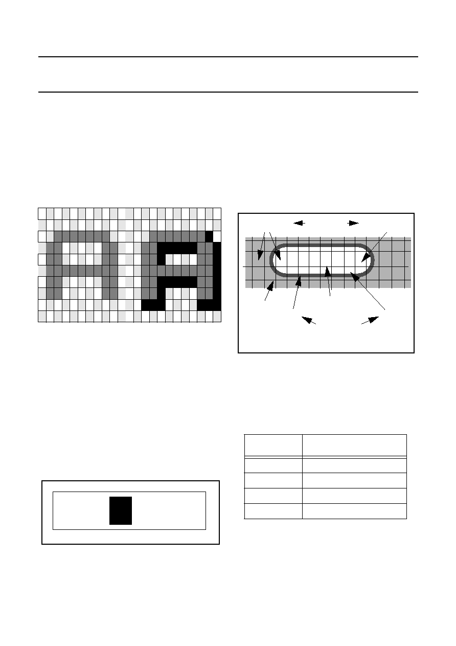
2000 Jun 22
47
Philips Semiconductors
Tentative Device Specification
TV signal processor-Teletext decoder with
embedded
µ
-Controller
TDA955X/6X/8X PS/N1 series
pixel from scan line to scan line, thus achieving a checker
board display of the background colour and video.
TXT: There are two meshing attributes one that only
affects black background colours TXT4.BMESH and a
second that only affects backgrounds other than black
TXT4.CMESH. A black background is defined as CLUT
entry 8, a none black background is defined as CLUT entry
9-15.
CC: The setting of the Mesh bit in REG0:Display Control
has the effect of meshing any background colour.
Fig.17 Meshing and Meshing / Fringing (South+West)
C
URSOR
The cursor operates by reversing the background and
foreground colours in the character position pointed to by
the active cursor position. The cursor is enabled using
TXT7.CURSOR ON. When active, the row the cursor
appears on is defined by TXT9.R<4:0> and the column is
defined by TXT10.C<5:0>. The position of the cursor can
be fixed using TXT9.CURSOR FREEZE.
CC: The valid range for row is 0 to 15. The valid range for
column is 0 to 47. The cursor remains rectangular at all
times, it's shape is not affected by italic attribute, therefore
it is not advised to use the cursor with italic characters.
TXT: The valid range for row positioning is 0 to 24.The
valid range for column is 0 to 39.
S
PECIAL
G
RAPHICS
C
HARACTERS
CC/TXT: Several special characters are provided for
improved OSD effects. These characters provide a choice
of 4 colours within a character cell. The total number of
special graphics characters is limited to 16. They are
stored in the character codes 8Xh and 9Xh of the character
table (32 ROM characters), or in the DRCs which overlay
character codes 8Xh and 9Xh. Each special graphics
character uses two consecutive normal characters.
Fringing, underline and overline is not possible for special
graphics characters. Special graphics characters are
activated when TXT21.OSD_PLANE = 1.
The example in Fig.19 can be done with 8 special graphics
characters.
If the screen colour is transparent (implicit in mixed mode)
and inside the object the box attribute is set, then the
object is surrounded by video. If the box attribute is not set
the background colour inside the object will also be
displayed as transparent.
A B
C
D E F
Fig.18 Cursor Display
Plane
1 0
Colour Allocation
0 0
Background Colour
0 1
Foreground Colour
1 0
CLUT entry 6
1 1
CLUT entry 7
Table 16 Special Character Colour allocation
VOLUME
Background Colour
Foreground Colour 7
Background Colour Serial Attribute
"set at" (Mode 0)
Background Colour
"set after" (Mode 1)
Foreground Colour
Normal Character
Foreground Colour 6
Special Character
Fig.19 Special Character Example

2000 Jun 22
48
Philips Semiconductors
Tentative Device Specification
TV signal processor-Teletext decoder with
embedded
µ
-Controller
TDA955X/6X/8X PS/N1 series
Character and Attribute Coding
CC M
ODE
Character coding is split into character oriented attributes (parallel) and character group coding (serial). The serial
attributes take effect either at the position of the attribute (Set At), or at the following location (Set After) and remain
effective until either modified by a new serial attribute or until the end of the row. A serial attribute is represented as a
space (the space character itself however is not used for this purpose), the attributes that are still active, e.g. overline
and underline will be visible during the display of the space. The default setting at the start of a row is:
∑
1x size, flash and italics OFF
∑
overline and underline OFF
∑
Display mode = superimpose
∑
fringing OFF
∑
background colour duration = 0
∑
end of row = 0
The coding is done in 12 bit words. The codes are stored sequentially in the display memory. A maximum of 768
character positions can be defined for a single display.
P
ARALLEL
C
HARACTER
C
ODING
Bits
Description
0-7
8 bit character code
8-10
3 bits for 8 foreground colours
11
Mode bit:
0 = Parallel code
Table 17 Parallel Character Coding

2000 Jun 22
49
Philips Semiconductors
Tentative Device Specification
TV signal processor-Teletext decoder with
embedded
µ
-Controller
TDA955X/6X/8X PS/N1 series
S
ERIAL
C
HARACTER
C
ODING
Table 18 Serial Character Coding
TXT M
ODE
Character coding is in a serial format, with only one
attributes being changed at any single location. The serial
attributes take effect either at the position of the attribute
(Set At), or at the following location (Set After). The
attribute remainseffective until either modified by new
serial attributes or until the end of the row.The default
settings at the start of a row is:
∑
foreground colour white (CLUT Address 7)
∑
background colour black (CLUT Address 8)
Bits
Description
Serial Mode 0
("set at")
Serial Mode 1
Char.Pos. 1 ("set at")
Char.Pos. >1 ("set after")
0-3
4 bits for 16 Background
colours
4 bits for 16 Background colours
4 bits for 16 Background colours
4
0 = Underline OFF
1 = Underline ON
Horizontal Size:
0 = normal
1 = x2
0 = Underline OFF
1 = Underline ON
5
0 = Overline OFF
1 = Overline ON
Vertical Size:
0 = normal
1 = x2
0 = Overline OFF
1 = Overline ON
6
Display mode:
0 = Superimpose
1 = Boxing
Display mode:
0 = Superimpose
1 = Boxing
Display mode:
0 = Superimpose
1 = Boxing
7
0 = Flash OFF
1 = Flash ON
Foreground colour switch
0 = Bank 0 (colours 0-7)
1 = Bank 1 (colours 8-15)
Foreground colour switch
0 = Bank 0 (colours 0-7)
1 = Bank 1 (colours 8-15)
8
0 = Italics OFF
1 = Italics ON
Background colour duration:
0 = stop BGC
1 = set BGC to end of row
Background colour duration
(set at):
0 = stop BGC
1 = set BGC to end of row
9
0 = Fringing OFF
1 = Fringing ON
End of Row
0 = Continue Row
1 = End Row
End of Row (set at):
0 = Continue Row
1 = End Row
10
Switch for Serial coding
mode 0 and 1:
0 = mode 0
Switch for Serial coding mode 0
and 1:
1 = mode 1
Switch for Serial coding mode 0
and 1:
1 = mode 1
11
Mode bit:
1 = Serial code
Mode bit:
1 = Serial code
Mode bit:
1 = Serial code
2000 Jun 22
50
Philips Semiconductors
Tentative Device Specification
TV signal processor-Teletext decoder with
embedded
µ
-Controller
TDA955X/6X/8X PS/N1 series
∑
Horizontal size x1, Vertical size x1 (normal size)
∑
Alphanumeric ON
∑
Contiguous Mosaic Graphics
∑
Release Mosaics
∑
Flash, Box, Conceal and Twist OFF
The attributes have individual codes which are defined in the basic character table below:
Fig.20 TXT Basic Character Set (Pan-European)
0
1
2
3
4
5
6
7
8
9
A
B
C
D
E
F
0
1
2
3
4 5 6
7a 8 8a
A
B
C
2a
3a
6a 7
0 0 0 0
0 0 0 1
0 0 1 0
0 0 1 1
alpha
black
alpha
red
alpha
green
alpha
yellow
alpha
blue
alpha
magenta
alpha
cyan
alpha
white
graphics
red
graphics
green
graphics
yellow
graphics
blue
graphics
magenta
graphics
cyan
graphics
white
flash
steady
end
box
start
box
normal
height
double
height
double
width
double
size
conceal
display
contiguous
graphics
separated
graphics
black
bkgnd
new
bkgnd
hold
graphics
release
graphics
bkgnd
black
bkgnd
red
bkgnd
green
bkgnd
yellow
bkgnd
blue
bkgnd
magenta
bkgnd
cyan
bkgnd
white
norm sz
OSD
dbl ht
OSD
dbl wd
OSD
dbl sz
OSD
column
ro
w
bits
b7
b6
b5
b4
b3 b2 b1 b0
graphics
black
0 1 0 0
0 1 0 1
0 1 1 0
0 1 1 1
1 0 0 0
1 0 0 1
1 0 1 0
1 0 1 1
1 1 0 0
1 1 0 1
1 1 1 0
1 1 1 1
D E F
0
0
0
0
1
0
0
0
0
1
0
0
1
1
0
0
0
1
1
0
1
1
1
0
0
0
1
0
1
0
1
0
0
1
0
1
1
1
0
1
0
0
1
1
1
0
1
1
0
1
1
1
1
1
1
1
D E F
1
0
1
1
0
1
1
1
1
1
1
1
E/W = 0
E/W = 1
Nat
Opt
Nat
Opt
Nat
Opt
Nat
Opt
Nat
Opt
Nat
Opt
Nat
Opt
Nat
Opt
Nat
Opt
Nat
Opt
Nat
Opt
Nat
Opt
Nat
Opt
O
S
D
O
S
D
O
S
D
O
S
D
O
S
D
O
S
D
O
S
D
O
S
D
O
S
D
O
S
D
O
S
D
O
S
D
O
S
D
O
S
D
O
S
D
O
S
D
O
S
D
O
S
D
O
S
D
O
S
D
O
S
D
O
S
D
O
S
D
O
S
D
O
S
D
O
S
D
O
S
D
O
S
D
O
S
D
O
S
D
O
S
D
O
S
D
9a
O
S
D
O
S
D
O
S
D
O
S
D
O
S
D
O
S
D
O
S
D
O
S
D
O
S
D
O
S
D
O
S
D
O
S
D
O
S
D
O
S
D
O
S
D
O
S
D
9
O
S
D
O
S
D
O
S
D
O
S
D
O
S
D
O
S
D
O
S
D
O
S
D
O
S
D
O
S
D
O
S
D
O
S
D
O
S
D
O
S
D
O
S
D
O
S
D
1
0
0
1
0
0
0
1
twist

2000 Jun 22
51
Philips Semiconductors
Tentative Device Specification
TV signal processor-Teletext decoder with
embedded
µ
-Controller
TDA955X/6X/8X PS/N1 series
Screen and Global Controls
A number of attributes are available that affect the whole
display region, and cannot be applied selectively to
regions of the display.
TV
SCAN LINES PER
ROW
The number of TV scan lines per field used for each
display row can be defined, the value is independent of the
character size being used. The number of lines can be
either 10/13/16 per display row. The number of TV scan
lines per row is defined TXT21.DISP_LINES<1:0>.
A value of 9 lines per row can be achieved if the display is
forced into 525 line display mode by
TXT17.DISP_FORCE<1:0>, or if the device is in 10 line
mode and the automatic detection circuitry within display
finds 525 line display syncs.
C
HARACTER
M
ATRIX
(H
X
V)
There are four different character matrices available, these
are 12x10, 12x13, and 12x16. The selection is made using
TXT21.CHAR_SIZE<1:0> and is independent of the
number of display lines per row.
If the character matrix is less than the number of TV scan
lines per row then the matrix is padded with blank lines. If
the character matrix is greater than the number of TV scan
lines then the character is truncated.
D
ISPLAY
M
ODES
CC: When attributes superimpose or when boxing (see
Table 18, Serial Mode 0/1, bit 6) is set, the resulting display
depends on the setting of the following screen control
mode bits in REG0:Display Control.
Table 19 Display Modes
TXT: The display mode is controlled by the bits in the TXT5
and TXT6. There are 3 control functions - Text on,
Background on and Picture on. Separate sets of bits are
used inside and outside Teletext boxes so that different
display modes can be invoked. TXT6 is used if the
newsflash (C5) or subtitle (C6) bits in row 25 of the basic
page memory are set otherwise TXT5 is used. This allows
the software to set up the type of display required on
newsflash and subtitle pages (e.g. text inside boxes, TV
picture outside) this will be invoked without any further
software intervention when such a page is acquired.
Display Mode
MOD
1 0
Description
Video
0 0
Video mode disables all display
activities and sets the RGB to true
black and VDS to video.
Full Text
0 1
Full Text mode displays screen
colour at all locations not covered by
character foreground or background
colour. The box attribute has no
effect.
Mixed Screen
Colour
1 0
Mixed Screen mode displays screen
colour at all locations not covered by
character foreground, within boxed
areas or, background colour.
Mixed Video
1 1
Mixed Video mode displays video at
all locations not covered by
character foreground, within boxed
areas or, background colour.
Picture On
Text On
Background
On
Effect
0
0
x
Text mode, black screen
0
1
0
Text mode, background always black
0
1
1
Text mode
1
0
x
Video mode
1
1
0
Mixed text and TV mode
1
1
1
Text mode, TV picture outside text area
Table 20 TXT Display Control Bits
2000 Jun 22
52
Philips Semiconductors
Tentative Device Specification
TV signal processor-Teletext decoder with
embedded
µ
-Controller
TDA955X/6X/8X PS/N1 series
Screen Colour
Screen colour is displayed from 10.5 ms to 62.5 ms after
the active edge of the HSync input and on TV lines 23 to
310 inclusive, for a 625 line display, and lines 17 to 260
inclusive for a 525 line display.
The screen colour is defined by REG0:Display Control and
points to a location in the CLUT table. The screen colour
covers the full video width. It is visible when the Full Text
or Mixed Screen Colour mode is set and no foreground or
background pixels are being displayed.
Text Display Controls
T
EXT
D
ISPLAY
C
ONFIGURATION
Two types of area are possible. The one area is static and
the other is dynamic. The dynamic area allows scrolling of
a region to take place. The areas cannot cross each other.
Only one scroll region is possible.
Display Map
The display map allows a flexible allocation of data in the
memory to individual rows.
Sixteen words are provided in the display memory for this
purpose. The lower 10 bits address the first word in the
memory where the row data starts. This value is an offset
in terms of 16-bit words from the start of Display Memory
(8000 Hex). The most significant bit enables the display
when not within the scroll (dynamic) area.
The display map memory is fixed at the first 16 words in
the closed caption display memory.
S
OFT
S
CROLL
A
CTION
The dynamic scroll region is defined by the REG5:Scroll
Area, REG6:Scroll Range, REG14:Top Scroll line and the
REG8:Status Register. The scroll area is enabled when
the SCON bit is set in REG8: Status.
The position of the soft scroll area window is defined using
the Soft Scroll Position (SSP<3:0), and the height of the
window is defined using the Soft Scroll Height (SSH<3:0>)
both are in REG6:Scroll Range. The rows that are scrolled
through the window are defined using the Start Scroll Row
(STS<3:0>) and the Stop Scroll Row (SPS<3:0>) both are
in REG5:Scroll Area.
The soft scrolling function is done by modifying the Scroll
Line (SCL<3:0>) in REG14: Top Scroll Line. and the first
scroll row value SCR<3:0> in REG8:Status. If the number
of rows allocated to the scroll counter is larger than the
defined visible scroll area, this allows parts of rows at the
top and bottom to be displayed during the scroll function.
The registers can be written throughout the field and the
values are updated for display with the next field sync.
Care should be taken that the register pairs are written to
by the software in the same field.
Only a region that contains only single height rows or only
double height rows can be scrolled.
b11 b10
b9
b8
b7
b6
b5
b4
b3
b2
b1
b0
Pointer to Row Data
Reserved, should be set to 0
Text Display Enable, valid outside Soft Scroll Area
0 = Disable
1 = Enable
Table 21 Display map Bit Allocation
Display Memory
Text Area
ROW
1
2
3
4
5
6
7
8
9
10
11
12
13
14
15
0
1
2
3
4
5
6
7
8
9
10
11
12
13
14
15
0
Display Map Entries
Display Data
Enable bit = 0
Display
possible
Display
possible
Soft Scrolling
display possible
Fig.21 Display Map and Data Pointers
2000 Jun 22
53
Philips Semiconductors
Tentative Device Specification
TV signal processor-Teletext decoder with
embedded
µ
-Controller
TDA955X/6X/8X PS/N1 series
Display Positioning
The display consists of the Screen Colour covering the
whole screen and the Text Area that is placed within the
visible screen area. The screen colour extends over a
large vertical and horizontal range so that no offset is
needed. The text area is offset in both directions relative to
the vertical and horizontal sync pulses.
S
CREEN
C
OLOUR
D
ISPLAY
A
REA
This area is covered by the screen colour. The screen
colour display area starts with a fixed offset of 8 us from
the leading edge of the horizontal sync pulse in the
horizontal direction. A vertical offset is not necessary.
T
EXT
D
ISPLAY
A
REA
The text area can be defined to start with an offset in both
the horizontal and vertical direction.
The horizontal offset is set in REG2: Text Area Start. The
offset is done in full width characters using TAS<5:0> and
quarter characters using HOP<1:0> for fine setting. The
ROW
1
2
3
4
5
6
7
8
9
10
11
12
13
14
15
0
Soft Scroll Position
Pointer SSP<3:0> e.g. 6
Soft Scroll Height
SSH<3:0> e.g.4
Start Scroll Row
Stop Scroll Row
Usable for OSD Display
Should not be used for
Should not be used for
Usable for OSD Display
Soft Scrolling Area
OSD Display
OSD Display
STS<3:0> e.g. 3
SPS<3:0> e.g. 11
Fig.22 Soft Scroll Area
Closed Captioning data row n
Closed Captioning data row n+1
Closed Captioning data row n+2
Closed Captioning data row n+3
Closed Captioning data row n+4
ROW
1
2
3
4
5
6
7
8
9
10
11
12
13
14
15
0
P01 NBC
0-63 lines
Visible area
for scrolling
Scroll Area
Offset
row1
row0
row2
row3
row4
row5
row6
row7
row8
row13
row14
Fig.23 CC Text Areas
Horizontal
starts 8 us after the leading edge of H-Sync for 56
us.
Vertical
line 9, field 1 (321, field 2) with respect to leading
edge of vertical sync (line numbering using 625
Standard).
Table 22 Screen Colour Display Area
Horizontal
Up to 48 full sized characters per row.
Start position setting from 3 to 64 characters from
the leading edge of H-Sync. Fine adjustment in
quarter characters.
Vertical
256 lines (nominal 41- 297).
Start position setting from leading edge of vertical
sync legal values are 4 to 64 lines.
(line numbering using 625 Standard)
Table 23 Text Display Area
Horizontal Sync.
Vertical
Text Area
Screen Colour Area
Text Area Start
56
µ
s
Sync.
0.25 char. offset
Text Area End
Screen Colour Offset = 8
µ
s
Text
Vertical
Offset
6 Lines
Offset
H-Sync delay
Fig.24 Display Area Positioning

2000 Jun 22
54
Philips Semiconductors
Tentative Device Specification
TV signal processor-Teletext decoder with
embedded
µ
-Controller
TDA955X/6X/8X PS/N1 series
values 00h to 03h for TAS<5:0> will result in a corrupted
display.
The width of the text area is defined in REG4:Text Area
End by setting the end character value TAE<5:0>. This
number determines where the background colour of the
Text Area will end if set to extend to the end of the row. It
will also terminate the character fetch process thus
eliminating the necessity of a row end attribute. This
entails however writing to all positions.
The vertical offset is set in REG1:Text Position Vertical
Register. The offset value VOL<5:0> is done in number of
TV scan lines.
NOTE: REG1:Text Position Vertical Register should not
be set to 00 Hex as the Display Busy interrupt is not
generated in these circumstances.
Character Set
To facilitate the global nature of the device the character
set has the ability to accommodate a large number of
characters, which can be stored in different matrices.
C
HARACTER
M
ATRICES
The character matrices that can be accommodated are: -
(HxVxPlanes) 12x9x1, 12x10x1, 12x13x1, 12x16x1.
These modes allow two colours per character position.
In CC mode two additional character matrices are
available to allow four colours per character: -
(HxVxPlanes) 12x13x2, 12x16x2.
The characters are stored physically in ROM in a matrix of
size either 12x10 or 12x16.
C
HARACTER
S
ET
S
ELECTION
Four character sets are available in the device. A set can
consist of alphanumeric characters as required by the
WST Teletext or FCC Closed Captioning, Customer
definable On-Screen Display characters, and Special
Graphic characters.
CC:- Only a single character set can be used for display
and this is selected using the Basic Set selection
TXT18.BS<1:0>. When selecting a character set in CC
mode the Twist Set selection TXT18.TS<1:0> should be
set to the same value as TXT18.BS<1:0> for correct
operation.
TXT:- Two character sets can be displayed at once. These
are the basic G0 set or the alternative G0 set (Twist Set).
The basic set is selected using TXT18.BS<1:0>, The
alternative/twist character set is defined by
TXT19.TS<1:0>. Since the alternative character set is an
option it can be enabled or disabled using TXT19.TEN,
and the language code that is defined for the alternative
set is defined by TXT19.TC<2:0>.
ROM A
DDRESSING
Three ROM's are used to generate the correct pixel
information. The first contains the National Option look-up
table, the second contains the Basic Character look-up
table and the third contains the Character Pixel
information. Although these are individual ROM, since
they do not need to be accessed simultaneously they are
all combined into a single ROM unit.
Fig.25 ROM Organisation
CHAR PIXEL
DATA
LOOK-UP
Basic + Nat Opt
0000H
0800H
2400H
2048 location
Approx. 710 Text
or
71680 x 12 bits
430Text +176CC
Look-Up Set 0
Look-Up Set1
Look-Up Set2
Look-Up Set3
0000
0200
0400
0600
0800

2000 Jun 22
55
Philips Semiconductors
Tentative Device Specification
TV signal processor-Teletext decoder with
embedded
µ
-Controller
TDA955X/6X/8X PS/N1 series
C
HARACTER
T
ABLE
The character table is shown in Table 24:-
Re-definable Characters
A number of Dynamically Re-definable Characters (DRC) are available. These are mapped onto the normal character
codes, and replace the pre-defined OTP character Rom value.
There are 32 DRCs which occupy character codes 80H to 9FH. Alternatively, These locations can be utilized as 16
special graphics characters. The remapping of the standard OSD to the DRCs is activated when the TXT21.DRCS
ENABLE bit is set. The selection of Normal or Special OSD symbols is defined by the TXT21.OSD PLANES.
Each character is stored in a matrix of 16x16x1 (V x H x planes), this allows for all possible character matrices to be
defined within a single location.
Character code columns (Bits 4-7)
0
1
2
3
4
5
6
7
8
9
A
B
C
D
E
F
Character code rows (Bits 0-3)
0
Æ
SP
0
@
P
˙
p
1
∞
!
1
A
Q
a
q
2
1/2
"
2
B
R
b
r
3
ø
#
3
C
S
c
s
4
TM
$
4
D
T
d
t
5
¢
%
5
E
U
e
u
6
£
&
6
F
V
f
v
7
¥
7
G
W
g
w
8
ý
(
8
H
X
h
x
9
_
)
9
I
Y
i
y
A
Ë
·
:
J
Z
j
z
B
‚
+
;
K
[
k
Á
C
Í
,
<
L
È
l
D
Ó
-
=
M
]
m
—
E
Ù
.
>
N
Ì
n
Ò
F
˚
/
?
O
Û
o
n
Table 24 Closed Caption Character Table
Special Characters are in column 8.
Additional table locations for normal characters
Table locations for normal characters
2000 Jun 22
56
Philips Semiconductors
Tentative Device Specification
TV signal processor-Teletext decoder with
embedded
µ
-Controller
TDA955X/6X/8X PS/N1 series
D
EFINING
C
HARACTERS
The DRC RAM is mapped on to the 80C51 RAM address
space and starts at location 8800H. The character matrix
is 12 bits wide and therefore requires two bytes to be
written for each word, the first byte (even addresses),
addresses the lower 8 bits and the second byte (odd
addresses) addresses the upper 4 bits.
For characters of 9, 10 or 16 lines high the pixel
information starts in the first address and continues
sequentially for the required number of addresses.
Characters of 13 lines high are defined with an initial offset
of 1 address, this is to allow for correct generation of
fringing across boundaries of clustered characters (see
Fig.27). The characters continue sequentially for 13 lines
after which a further line can again be used for generation
of correct fringing across boundaries of clustered
characters.
DRCs are defined by writing data to the DRC RAM using
the 80C51 MOVX command. Setting bits 3 to 9 of the first
line of a 12 wide by 16 line character would require setting
the high byte of the 80C51 data pointer to 88H, the low
byte of the 80C51 data pointer to 00H, using the MOVX
command to load address 8800H with data F8H,
incrementing the data pointer, and finally using the MOVX
command to load address 8801H with data 03H.
Display Synchronization
The horizontal and vertical synchronizing signals from the
TV deflection are used as inputs. Both signals can be
inverted before being delivered to the Phase Selector
section.
CC: The polarity is controlled using either VPOL or HPOL
in REG2:Text position Vertical.
TXT: SFRs bits TXT1.HPOL & TXT1.VPOL control the
polarity.
A line locked 12 MHz clock is derived from the 12MHz free
running oscillator by the Phase Selector. This line locked
clock is used to clock the whole of the Display block.
The H & V Sync signals are synchronized with the 12 MHz
clock before being used in the display section.
Video/Data Switch (Fast Blanking) Polarity
The polarity of the Video/Data (Fast Blanking) signal can
be inverted. The polarity is set with the VDSPOL in REG7:
RGB Brightness register.
Video/Data Switch Adjustment
To take into account the delay between the RGB values
and the VDS signal due to external buffering, the VDS
signal can be moved in relation to the RGB signals. The
VDS signal can be set to be either a clock cycle before or
after the RGB signal, or coincident with the RGB signal.
This is done using VDEL<2:0> in REG15:Configuration.
CHAR 1
CHAR 2
CHAR 30
CHAR 31
CHAR 0
A
00
01
02
03
04
05
06
07
08
09
0A
0B
0C
0D
0E
0F
CHAR 0
Address
12 bits
Micro Address
8800
881F
8820
883F
8840
885F
8BFF
8BE0
8BDF
8BC0
Char Code
80h
81h
82h
9Eh
9Fh
Fig.26 Organisation of DRC RAM
Top Left
Bottom Right
Fringing
Top Line
Hex
003
00C
030
0C0
300
C00
C00
300
C00
030
00C
003
000
440
Line 13 from
character above
Line 1 from
character below
Fringing
1A8
000
Pixel
Pixel
Line not used
Line
No.
0
1
2
3
4
5
6
7
8
9
10
11
12
13
14
15
Bottom Line
MSB
LSB
Fig.27 13 Line High DRC's Character Format
VDSP
OL
VDS
Condition
0
1
RGB display
0
0
Video Display
1
0
RGB display
1
1
Video Display
Table 25 Fast Blanking Signal Polarity

2000 Jun 22
57
Philips Semiconductors
Tentative Device Specification
TV signal processor-Teletext decoder with
embedded
µ
-Controller
TDA955X/6X/8X PS/N1 series
RGB Brightness Control
A brightness control is provided to allow the RGB upper
output voltage level to be modified. The RGB amplitude
may be varied between 60% and 100%.
The brightness is set in the RGB Brightness register as
follows: -
Contrast Reduction
TXT: The COR bits in SFRs TXT5 & TXT6 control when
the COR output of the device is activated (i.e. Pulled-low).
This output is intended to act on the TV's display circuits to
reduce contrast of the video when it is active. The result of
contrast reduction is to improve the readability of the text
in a mixed teletext and video display.
The bits in the TXT5 & TXT6 SFRs allow the display to be
set up so that, for example, the areas inside teletext boxes
will be contrast reduced when a subtitle is being displayed
but that the rest of the screen will be displayed as normal
video.
CC: This feature is not available in CC mode.
Memory Mapped Registers
The memory mapped registers are used to control the
display. The registers are mapped into the Microcontroller
MOVX address space, starting at address 87F0h and
extending to 87FF.
MMR M
AP
BRI3-0
RGB Brightness
0 0 0 0
Lowest value
...
...
1 1 1 1
Highest value
Table 26 RGB Brightness
ADD
R/W
Names
BIT7
BIT6
BIT5
BIT4
BIT3
BIT2
BIT1
BIT0
87F0
R/W
Display Control
SRC<3>
SRC<2>
SRC<1>
SRC<0>
-
MSH
MOD<1>
MOD<0>
87F1
R/W
Text
Position
Vertical
VPOL
HPOL
VOL<5>
VOL<4>
VOL<3>
VOL<2>
VOL<1>
VOL<0>
87F2
R/W
Text Area Start
HOP<1>
HOP<0>
TAS<5>
TAS<4>
TAS<3>
TAS<2>
TAS<1>
TAS<0>
87F3
R/W
Fringing Control
FRC<3>
FRC<2>
FRC<1>
FRC<0>
FRDN
FRDE
FRDS
FRDW
87F4
R/W
Text Area End
-
-
TAE<5>
TAE<4>
TAE<3>
TAE<2>
TAE<1>
TAE<0>
87F5
R/W
Scroll Area
SSH<3>
SSH<2>
SSH<1>
SSH<0>
SSP<3>
SSP<2>
SSP<1>
SSP<0>
87F6
R/W
Scroll Range
SPS<3>
SPS<2>
SPS<1>
SPS<0>
STS<3>
STS<2>
STS<1>
STS<0>
87F7
R/W
RGB Bright.ness
VDSPOL
-
-
-
BRI<3>
BRI<2>
BRI<1>
BRI<0>
87F8
R
Status read
BUSY
FIELD
SCON
FLR
SCR<3>
SCR<2>
SCR<1>
SCR<0>
87F8
W
Status write
-
-
SCON
FLR
SCR<3>
SCR<2>
SCR<1>
SCR<0>
87FC
R/W
H-Sync. Delay
-
HSD<6>
HSD<5>
HSD<4>
HSD<3>
HSD<3>
HSD<1>
HSD<0>
87FD
R/W
V-Sync. Delay
-
VSD<6>
VSD<5>
VSD<4>
VSD<3>
VSD<2>
VSD<1>
VSD<0>
87FE
R/W
Top Scroll Line
-
-
-
-
SCL<3>
SCL<2>
SCL<1>
SCL<0>
87FF
R/W
Configuration
CC
VDEL<2>
VDEL<1>
VDEL<0>
TXT/V
-
-
-
Table 27 MMR Memory Map

2000 Jun 22
58
Philips Semiconductors
Tentative Device Specification
TV signal processor-Teletext decoder with
embedded
µ
-Controller
TDA955X/6X/8X PS/N1 series
MMR B
IT DEFINITION
Names
BIT7
BIT6
BIT5
BIT4
BIT3
BIT2
BIT1
BIT0
RESET
Display Control.
SRC<3>
SRC<2>
SRC<1>
SRC<0>
-
MSH
MOD<1>
MOD<0>
00H
SRC<3:0>
Screen Colour definition
MSH
0 - No meshing of background
1 - Meshing all background colours
MOD<1:0>
00 - Video
01 - Full Text
10 - Mixed Screen Colour
11 - Mixed Video
Text Position
Vertical
VPOL
HPOL
VOL<5>
VOL<4>
VOL<3>
VOL<2>
VOL<1>
VOL<0>
00H
VPOL
0 - Input polarity
1 - Inverted input polarity
HPOL
0 - Input Polarity
1 - Inverted input polarity
VOL<5:0>
Display start Vertical Offset from V-Sync. (lines)
Text Area Start
HOP<1>
HOP<0>
TAS<5>
TAS<4>
TAS<3>
TAS<2>
TAS<1>
TAS<0>
00H
HOP<1:0>
Fine Horizontal Offset in quarter of characters
TAS<5:0>
Text area start
Fringing Control.
FRC<3>
FRC<2>
FRC<1>
FRC<0>
FRDN
FRDE
FRDS
FRDW
00H
FRC<3:0>
Fringing colour, value address of CLUT
FRDN
0 - No fringe in North direction
1 - Fringe in North direction
FRDE
0 - No fringe in East direction
1 - Fringe in East direction
FRDS
0 - No fringe in South direction
1 - Fringe in South direction
FRDW
0 - No fringe in West direction
1 - Fringe in West direction
Text Area End
-
-
TAE<5>
TAE<4>
TAE<3>
TAE<2>
TAE<1>
TAE<0>
00H
TAE<5:0>
Text Area End, in full characters
Scroll Area
SSH<3>
SSH<2>
SSH<1>
SSH<0>
SSP<3>
SSP<2>
SSP<1>
SSP<0>
00H
SSH<3:0>
Soft Scroll Height
SSP<3:0>
Soft Scroll Position
Scroll Range
SPS<3>
SPS<2>
SPS<1>
SPS<0>
STS<3>
STS<2>
STS<1>
STS<0>
00H
SPS<3:0>
Stop Scroll row
STS<3:0>
Start Scroll row
RGB Brightness
VDSPOL
-
-
-
BRI<3>
BRI<2>
BRI<1>
BRI<0>
00H

2000 Jun 22
59
Philips Semiconductors
Tentative Device Specification
TV signal processor-Teletext decoder with
embedded
µ
-Controller
TDA955X/6X/8X PS/N1 series
Table 28 MMR Descriptions
VDSPOL
VDS Polarity
0 - RGB (1), Video (0)
1 - RGB (0), Video (1)
BRI<3:0>
RGB Brightness control
Status read
BUSY
FIELD
SCON
FLR
SCR<3>
SCR<2>
SCR<1>
SCR<0>
00H
BUSY
0 - Access to display memory will not cause display problems
1 - Access to display memory could cause display problems.
FIELD
0 - Odd Field
1 - Even Field
FLR
0 - Active flash region foreground and background displayed
1 - Active flash region background only displayed
SCR<3:0>
First scroll row
Status write
-
-
SCON
FLR
SCR<3>
SCR<2>
SCR<1>
SCR<0>
00H
SCON
0 - Scroll area disabled
1 - Scroll area enabled
FLR
0 - Active flash region foreground and background colour displayed
1 - Active flash region background colour only displayed
SCR<3:0>
First Scroll Row
H-Sync. delay
-
HSD<6>
HSD<5>
HSD<4>
HSD<3>
HSD<3>
HSD<1>
HSD<0>
00H
HSD<6:0>
H-Sync delay, in full size characters
V-Sync Delay
-
VSD<6>
VSD<5>
VSD<4>
VSD<3>
VSD<2>
VSD<1>
VSD<0>
00H
VSD<6:0>
V-Sync delay in number of TV lines
Top Scroll Line
-
-
-
-
SCL<3>
SCL<2>
SCL<1>
SCL<0>
00H
SCL<3:0>
Top line for scroll
Configuration
CC
VDEL<2>
VDEL<1>
VDEL<0>
TXT/V
-
-
-
00H
CC
0 - OSD mode
1 - Closed Caption mode
VDEL<2:0>
Pixel delay between VDS and RGB output
000 - VDS switched to video, not active
001 - VDS active one pixel earlier then RGB
010 - VDS synchronous to RGB
100 - VDS active one pixel after RGB
TXT/V
BUSY Signal switch
1 - Horizontal
0 - Vertical

2000 Jun 22
60
Philips Semiconductors
Tentative Device Specification
TV signal processor-Teletext decoder with
embedded
µ
-Controller
TDA955X/6X/8X PS/N1 series
OTP MEMORY
These may be programmed either using the Parallel
Programming Interface or via the ISP Programming
Interface.
Parallel Programming
The following pins form the parallel programming
interface:-
ISecurity Bits
The family of devices have a set of security bits for the
combined OTP Program ROM, Character ROM and
Packet 26 ROM. The security bits are used to prevent the
ROM from being overwritten once programmed, and also
the contents being verified once programmed. The
security bits are one-time programmable and CANNOT be
erased.
Pin
Name
Function
P0.5
IO(0)
Bit 0:- Address/Data/Mode
P0.6
IO(1)
Bit 1:- Address/Data/Mode
P1.0
IO(2)
Bit 2:- Address/Data/Mode
P1.1
IO(3)
Bit 3:- Address/Data/Mode
P1.2
IO(4)
Bit 4:- Address/Data/Mode
P1.3
IO(5)
Bit 5:- Address/Data/Mode
P3.1
IO(6)
Bit 6:- Address/Data/Mode
P3.2
IO(7)
Bit 7:- Address/Data/Mode
P2.0
OEB
Output Enable
0 = IO is output
1 = IO is input
P3.0
WEB
Write
Enable,
programming
pulse
>100us
0 = Program
P1.6
MODE
0 = IO(7:0) defined by A/DB
1 = IO(7:0) contains mode information
P1.7
A/DB
0 = IO(7:0) contains Data
1
=
IO(7:0)
contains
Address
Information
P3.3
Unused
VPE
VPE
9V Programming Voltage
RESET
RESET
Device reset/ mode selection
XTALIN
CLK
Clock 4 MHz
Table 29 Parallel Programming Interface

2000 Jun 22
61
Philips Semiconductors
Tentative Device Specification
TV signal processor-Teletext decoder with
embedded
µ
-Controller
TDA955X/6X/8X PS/N1 series
The memory and security bits are structured as follows:-
Table 30 Security bit structure
The security bits are set as follows for production programmed devices (i.e. programmed by Philips):-
The security bits are set as follows for production un-programmed (blank) devices:-
MEMORY
SECURITY BITS INTERACTION
PROGRAM
ROM
USER ROM Programming
(Enable/Disable)
TEST ROM Programming
(Enable/Disable)
Verify
(Enable/Disable)
USER ROM
(i.e. 128k x 8 bits)
=
Yes
No
Yes
TEST ROM
RESERVED
(1k x 8 bits)
=
No
Yes
Yes
CHARACTER
ROM
USER ROM Programming
(Enable/Disable)
TEST ROM Programming
(Enable/Disable)
Verify
(Enable/Disable)
USER ROM
(9k x 12 bits)
=
Yes
No
Yes
TEST ROM
RESERVED
(0.5k x 12 bits)
=
No
Yes
Yes
PACKET 26
ROM
USER ROM Programming
(Enable/Disable)
TEST ROM Programming
(Enable/Disable)
Verify
(Enable/Disable)
USER ROM
(4k x 8 bits)
=
Yes
No
Yes
MEMORY
SECURITY BITS SET
USER ROM Programming
(Enable/Disable)
TEST ROM Programming
(Enable/Disable)
Verify
(Enable/Disable)
PROGRAM ROM
=
DISABLED
DISABLED
ENABLED
CHARACTER ROM
=
DISABLED
DISABLED
ENABLED
PACKET 26 ROM
=
DISABLED
DISABLED
ENABLED
Table 31 Security bits for production devices
MEMORY
SECURITY BITS SET
USER ROM Programming
(Enable/Disable)
TEST ROM Programming
(Enable/Disable)
Verify
(Enable/Disable)
PROGRAM ROM
=
ENABLED
DISABLED
ENABLED
CHARACTER ROM
=
ENABLED
DISABLED
ENABLED
PACKET 26 ROM
=
ENABLED
DISABLED
ENABLED
Table 32 Security bits for Blank devices

2000 Jun 22
62
Philips Semiconductors
Tentative Device Specification
TV signal processor-Teletext decoder with
embedded
µ
-Controller
TDA955X/6X/8X PS/N1 series

2000 Jun 22
63
Philips Semiconductors
Tentative Device Specification
TV signal processor-Teletext decoder with
embedded
µ
-Controller
TDA955X/6X/8X PS/N1 series
FUNCTIONAL DESCRIPTION OF VIDEO PROCESSOR
Vision IF amplifier
The vision IF amplifier can demodulate signals with
positive and negative modulation. The PLL demodulator is
completely alignment-free.
The VCO of the PLL circuit is internal and the frequency is
fixed to the required value by using the clock frequency of
the
µ
-Controller/Teletext decoder as a reference. The
setting of the various frequencies (38, 38.9, 45.75 and
58.75 MHz) can be made via the control bits IFA-IFC in
subaddress 27H. Because of the internal VCO the IF
circuit has a high immunity to EMC interferences.
QSS Sound circuit
The sound IF amplifier is similar to the vision IF amplifier
and has an external AGC decoupling capacitor.
The single reference QSS mixer is realised by a multiplier.
In this multiplier the SIF signal is converted to the
intercarrier frequency by mixing it with the regenerated
picture carrier from the VCO. The mixer output signal is
supplied to the output via a high-pass filter for attenuation
of the residual video signals. With this system a high
performance hi-fi stereo sound processing can be
achieved.
The AM sound demodulator is realised by a multiplier. The
modulated sound IF signal is multiplied in phase with the
limited SIF signal. The demodulator output signal is
supplied to the output via a low-pass filter for attenuation
of the carrier harmonics. The AM signal is supplied to the
output (AUDOUT/AMOUT) via the volume control.
Switching between the QSS output and AM output is made
by means of the AM bit in subaddress 29H (see also
Table 1).
FM demodulator
The FM demodulator is realised as narrow-band PLL with
external loop filter, which provides the necessary
selectivity without using an external band-pass filter. To
obtain a good selectivity a linear phase detector and a
constant input signal amplitude are required. For this
reason the intercarrier signal is internally supplied to the
demodulator via a gain controlled amplifier and AGC
circuit. To improve the selectivity an internal bandpass
filter is connected in front of the PLL circuit. This bandpass
filter can be switched off by means of the BPB bit in
subaddress 2CH.
The nominal frequency of the demodulator is tuned to the
required frequency (4.5/5.5/6.0/6.5 MHz) by means of a
calibration circuit which uses the clock frequency of the
µ
-Controller/Teletext decoder as a reference. It is also
possible to frequencies of 4.74 and 5.74 MHz so that a
second sound channel can be demodulated. In the latter
application an external bandpass filter has to be applied to
obtain sufficient selectivity (the sound input can be
activated by the SIF bit in subaddress 28H). The setting to
the wanted frequency is realised by means of the control
bits FMA, FMB and FMC in the control bit 29H.
From the output status bytes it can be read whether the
PLL frequency is inside or outside the window and whether
the PLL is in lock or not. With this information it is possible
to make an automatic search system for the incoming
sound frequency. This can be realised by means of a
software loop which switches the demodulator to the
various frequencies and then select the frequency on
which a lock condition has been found.
The deemphasis output signal amplitude is independent of
the TV standard and has the same value for a frequency
deviation of
±
25 kHz at the 4.5 MHz standard and for a
deviation of
±
50 Khz for the other standards.
In versions with QSS amplifier and mono intercarrier
sound circuit the FM radio mode is available. This mode is
activated by means of the FMR-bit (subaddress 2CH). The
selectivity must be made by means of a SAW filter at the
sound input with a centre frequency of 33.4 MHz for
Europe and 41.25 MHz for the USA. For this application
the IF demodulator must be set to a fixed frequency (42
MHz for Europe and 48 MHz for the USA). The resulting
input frequency for the FM demodulator is then 8.6 MHz for
Europe and 6.75 MHz for the USA. This frequency must be
selected by means of the bits FMA, FMB and FMC (see
table 108).
Audio circuit and input signal selection
The audio control circuit contains an audio switch with 1
external input and a volume control circuit. The selection
of the various inputs is made by means of the ADX bit. In
various versions the Automatic Volume Levelling (AVL)
function can be activated. The pin to which the external
capacitor has to be connected depends on the IC version.
For the 90
∞
types the capacitor is connected to the EW
output pin. For the 110
∞
types a choice must be made
between the AVL function and a sub-carrier output for
comb filter applications. This choice is made via the
CBM0/1 bits (in subaddress 22H). When the AVL is active
it automatically stabilises the audio output signal to a
certain level.
2000 Jun 22
64
Philips Semiconductors
Tentative Device Specification
TV signal processor-Teletext decoder with
embedded
µ
-Controller
TDA955X/6X/8X PS/N1 series
It is possible to use the deemphasis pin as additional audio
input. In that case the internal signal must, of course, be
switched off. This can be realised by means of the sound
mute bit (SM in subaddress 29H). When the IF circuit is
switched to positive modulation the internal signal on the
deemphasis pin is automatically muted.
CVBS and Y/C input signal selection
The circuit has 2 inputs for external CVBS signals and one
input can also be used as one Y/C input (see Fig. 27).
It is possible to supply the selected CVBS signal to the
demodulated IF video output pin. This mode is selected by
means of the SVO bit in subaddress 22H. The vision IF
amplifier is switched off in this mode.
The video ident circuit can be connected to the incoming
`internal' video signal or to the selected signal. This ident
circuit is independent of the synchronisation and can be
used to switch the time-constant of the horizontal PLL
depending on the presence of a video signal (via the VID
bit). In this way a very stable OSD can be realised.
The subcarrier output is combined with a 3-level output
switch (0 V, 2.3 V and 4.5 V). The output level and the
availability of the subcarrier signal is controlled by the
CMB1 and CMB0 bits. The output can be used to switch
sound traps etc. It is also possible to use this pin for the
connection of the AVL capacitor or as AM output.
TO LUMA/SYNC PROCESSING
TO CHROMA PROCESSING
CVBS2/Y
CVBS1
VIM
VIDEO IDENT
IDENT
Fig.27 CVBS switch and interfacing of video ident
C
(+)
IFVO
IFVO/SVO
SVO
Synchronisation circuit
The IC contains separator circuits for the horizontal and
vertical sync pulses and a data-slicing circuit which
extracts the digital teletext data from the analog signal.
The horizontal drive signal is obtained from an internal
VCO which is running at a frequency of 25 MHz. This
oscillator is stabilised to this frequency by using a 12 MHz
signal coming from the reference oscillator of the
µ
-Controller/Teletext decoder.
The horizontal drive is switched on and off via the soft
start/stop procedure. This function is realised by means of
variation of the T
ON
of the horizontal drive pulses. In
addition the horizontal drive circuit has a `low-power
start-up' function.
The vertical synchronisation is realised by means of a
divider circuit. The vertical ramp generator needs an
external resistor and capacitor. For the vertical drive a
differential output current is available. The outputs must be
DC coupled to the vertical output stage.
In the types which are intended for 90
∞
picture tubes the
following geometry parameters can be adjusted:
∑
Horizontal shift
∑
Vertical amplitude
∑
Vertical slope
∑
S-correction
∑
Vertical shift

2000 Jun 22
65
Philips Semiconductors
Tentative Device Specification
TV signal processor-Teletext decoder with
embedded
µ
-Controller
TDA955X/6X/8X PS/N1 series
The types which are intended to be used in combination
with 110
∞
picture tubes have an East-West control circuit
in stead of the AVL function. The additional controls for
these types are:
∑
EW width
∑
EW parabola width
∑
EW upper and lower corner parabola correction
∑
EW trapezium correction
∑
Vertical zoom
∑
horizontal parallelogram and bow correction.
When the vertical amplitude is compressed (zoom
factor <1) it is still possible to display the black current
measuring lines in the overscan. This function is activated
by means of the bit OSVE in subaddress 26H.
Chroma, luminance and feature processing
The chroma band-pass and trap circuits (including the
SECAM cloche filter) are realised by means of gyrators
and are tuned to the right frequency by comparing the
tuning frequency with the reference frequency of the
colour decoder. The luminance delay line and the delay
cells for the peaking circuit are also realised with gyrators.
The circuit contains the following picture improvement
features:
∑
Video dependent coring in the peaking circuit. The
coring can be activated only in the low-light parts of the
screen. This effectively reduces noise while having
maximum peaking in the bright parts of the picture.
∑
Black stretch. This function corrects the black level for
incoming signals which have a difference between the
black level and the blanking level.
∑
Blue-stretch. This circuit is intended to shift colour near
`white' with sufficient contrast values towards more blue
to obtain a brighter impression of the picture.
∑
Dynamic skin tone (flesh) control. This function is
realised in the YUV domain by detecting the colours
near to the skin tone.
Colour decoder
The ICs can decode PAL, NTSC and SECAM signals. The
PAL/NTSC decoder does not need external reference
crystals but has an internal clock generator which is
stabilised to the required frequency by using the 12 MHz
clock signal from the reference oscillator of the
µ
-Controller/Teletext decoder.
Under bad-signal conditions (e.g. VCR-playback in feature
mode), it may occur that the colour killer is activated
although the colour PLL is still in lock. When this killing
action is not wanted it is possible to overrule the colour
killer by forcing the colour decoder to the required standard
and to activate the FCO-bit (Forced Colour On) in
subaddress 21H.
The Automatic Colour Limiting (ACL) circuit (switchable
via the ACL bit in subaddress 20H) prevents that
oversaturation occurs when signals with a high
chroma-to-burst ratio are received. The ACL circuit is
designed such that it only reduces the chroma signal and
not the burst signal. This has the advantage that the colour
sensitivity is not affected by this function.
The SECAM decoder contains an auto-calibrating PLL
demodulator which has two references, viz: the divided 12
MHz reference frequency (obtained from the
µ
-Controller)
which is used to tune the PLL to the desired free-running
frequency and the bandgap reference to obtain the correct
absolute value of the output signal. The VCO of the PLL is
calibrated during each vertical blanking period, when the
IC is in search or SECAM mode.
The base-band delay line (TDA 4665 function) is
integrated. This delay line is also active during NTSC to
obtain a good suppression of cross colour effects. The
demodulated colour difference signals are internally
supplied to the delay line.

2000 Jun 22
66
Philips Semiconductors
Tentative Device Specification
TV signal processor-Teletext decoder with
embedded
µ
-Controller
TDA955X/6X/8X PS/N1 series
RGB output circuit and black-current stabilization
In the RGB control circuit the signal is controlled on
contrast, brightness and saturation. The ICs have a linear
input for external RGB/YUV signals. Switching between
RGB and the YUV/YP
R
P
B
mode can be realised via the
YUV0/YUV1 bits in subaddress 2BH. The signals for OSD
and text are internally supplied to the control circuit. The
output signal has an amplitude of about 2 V black-to-white
at nominal input signals and nominal settings of the
various controls.
To obtain an accurate biasing of the picture tube the
`Continuous Cathode Calibration' system has been
included in these ICs.
A black level off-set can be made with respect to the level
which is generated by the black current stabilization
system. In this way different colour temperatures can be
obtained for the bright and the dark part of the picture.
In the V
g2
adjustment mode (AVG = 1) the black current
stabilization system checks the output level of the 3
channels and indicates whether the black level of the
highest output is in a certain window (WBC-bit) or below or
above this window (HBC-bit). This indication can be read
from the status byte 01 and can be used for automatic
adjustment of the V
g2
voltage during the production of the
TV receiver. During this test the vertical scan remains
active so that the indication of the 2 bits can be made
visible on the TV screen.
The control circuit contains a beam current limiting circuit
and a peak white limiting circuit. The peak white level is
adjustable via the I
2
C-bus. To prevent that the peak white
limiting circuit reacts on the high frequency content of the
video signal a low-pass filter is inserted in front of the peak
detector. The circuit also contains a soft-clipper which
prevents that the high frequency peaks in the output signal
become too high. The difference between the peak white
limiting level and the soft clipping level is adjustable via the
I
2
C-bus in a few steps.
During switch-off of the TV receiver a fixed beam current
is generated by the black current control circuit. This
current ensures that the picture tube capacitance is
discharged. During the switch-off period the vertical
deflection can be placed in an overscan position so that
the discharge is not visible on the screen.
A wide blanking pulse can be activated in the RGB outputs
by means of the HBL bit in subaddress 2BH. The timing of
this blanking can be adjusted by means of the bits WBF/R
bits in subaddress 03H.
SOFTWARE CONTROL
The CPU communicates with the peripheral functions
using Special function Registers (SFRs) which are
addressed as RAM locations. The registers for the
Teletext decoder appear as normal SFRs in the
µ
-Controller memory map and are written to these
functions by using a serial bus. This bus is controlled by
dedicated hardware which uses a simple handshake
system for software synchronisation.
For compatibility reasons and possible re-use of software
blocks, the I
2
C-bus control for the TV processor is
organised as in the stand-alone TV signal processors. The
TV processor registers cannot be read, so when the
content of these registers is needed in the software, a copy
should be stored in Auxiliary RAM or Non Volatile RAM.
The slave address of the TV signal processor is given in
Fig.28.
Valid subaddresses: 03H to 2EH, subaddress FE and FF
are reserved for test purposes. Auto-increment mode
available for subaddresses.
handbook, halfpage
MLA743
A6
A5
A4
A3
A2
A1
A0
1
0
0
0
1
0
1
1/0
R/W
Fig.28 Slave address (8A).

2000 Jun 22
67
Philips Semiconductors
Tentative Device Specification
TV signal processor-Teletext decoder with
embedded
µ
-Controller
TDA955X/6X/8X PS/N1 series
DESCRIPTION OF THE I
2
C-BUS SUBADDRESSES
Table 33
Inputs TV-processor
Note
1. These functions are only available in versions which have the East-West drive output.
2. The AVL function is only available in versions which have no East-West output or when the subcarrier output is used for
the connection of the AVL capacitor (via the bits CMB1 and CMB0 in subaddress 22H).
3. Only available in types with QSS sound IF circuit and AM demodulator.
FUNCTION
SUBADDR
(HEX)
DATA BYTE
POR
D7
D6
D5
D4
D3
D2
D1
D0
Value
Timing of `wide blanking'
03
WBF3
WBF2
WBF1
WBF0
WBR3 WBR2 WBR1 WBR0
88
Peak white limiting
04
0
0
SOC1
SOC0
A3
A2
A1
A0
08
Off-set IF demodulator
05
0
0
A5
A4
A3
A2
A1
A0
20
Horizontal parallelogram
06
0
0
A5
A4
A3
A2
A1
A0
20
Horizontal bow
07
0
0
A5
A4
A3
A2
A1
A0
20
Hue
08
0
0
A5
A4
A3
A2
A1
A0
00
Horizontal shift (HS)
09
0
0
A5
A4
A3
A2
A1
A0
20
EW width (EW)
(1)
0A
0
0
A5
A4
A3
A2
A1
A0
20
EW parabola/width (PW)
(1)
0B
0
0
A5
A4
A3
A2
A1
A0
20
EW upper corner parabola
(1)
0C
0
0
A5
A4
A3
A2
A1
A0
20
EW lower corner parabola
(1)
0D
0
0
A5
A4
A3
A2
A1
A0
20
EW trapezium (TC)
(1)
0E
0
0
A5
A4
A3
A2
A1
A0
20
Vertical slope (VS)
0F
0
0
A5
A4
A3
A2
A1
A0
20
Vertical amplitude (VA)
10
0
0
A5
A4
A3
A2
A1
A0
20
S-correction (SC)
11
0
0
A5
A4
A3
A2
A1
A0
20
Vertical shift (VSH)
12
0
0
A5
A4
A3
A2
A1
A0
20
Vertical zoom (VX)
(1)
13
0
0
A5
A4
A3
A2
A1
A0
20
Black level offset R
14
0
0
A5
A4
A3
A2
A1
A0
20
Black level offset G
15
0
0
A5
A4
A3
A2
A1
A0
20
White point R
16
0
0
A5
A4
A3
A2
A1
A0
20
White point G
17
0
0
A5
A4
A3
A2
A1
A0
20
White point B
18
0
0
A5
A4
A3
A2
A1
A0
20
Peaking
19
PF1
PF0
A5
A4
A3
A2
A1
A0
20
Luminance delay time
1A
0
0
0
0
YD3
YD2
YD1
YD0
00
Brightness
1B
0
0
A5
A4
A3
A2
A1
A0
20
Saturation
1C
0
0
A5
A4
A3
A2
A1
A0
20
Contrast
1D
0
0
A5
A4
A3
A2
A1
A0
20
AGC take-over
1E
0
0
A5
A4
A3
A2
A1
A0
20
Volume control
1F
0
0
A5
A4
A3
A2
A1
A0
20
Colour decoder 0
20
CM3
CM2
CM1
CM0
MAT
MUS
ACL
CB
00
Colour decoder 1
21
0
0
0
0
0
0
BPS
FCO
00
AV-switch 0
22
0
0
SVO
CMB1
CMB0
INA
INB
INC
00
AV-switch 1
23
0
0
0
0
0
E2D
0
RGBL
00
Synchronisation 0
24
0
HP2
FOA
FOB
POC
STB
VIM
VID
00
Synchronisation 1
25
0
0
FSL
OSO
FORF
FORS
DL
NCIN
00
Deflection
26
OSVE
AFN
DFL
XDT
SBL
AVG
EVG
HCO
(1)
00
Vision IF 0
27
IFA
IFB
IFC
VSW
MOD
AFW
IFS
STM
00
Vision IF 1
28
SIF
IFE
AGCM
IFLH
AMFM AGC1
AGC0
FFI
00
Sound 0
29
AGN
SM1
FMWS
AM
(3)
SM0
FMC
FMB
FMA
00
Control 0
2A
0
IE2
RBL
AKB
CL3
CL2
CL1
CL0
00
Control 1
2B
0
0
0
SOY
0
YUV1
YUV0
HBL
(1)
00
Sound 1
2C
FMD
0
ADX
0
FMR
AVL
(2)
QSS
FMI
00
Features 0
2D
0
0
COR1
COR0
DSK
0
BLS
BKS
00
Features 1
2E
0
0
RPO1
RPO0
0
0
0
0
00

2000 Jun 22
68
Philips Semiconductors
Tentative Device Specification
TV signal processor-Teletext decoder with
embedded
µ
-Controller
TDA955X/6X/8X PS/N1 series
Table 34 Outputs TV-processor
FUNCTION
SUBADDR
DATA BYTE
D7
D6
D5
D4
D3
D2
D1
D0
Output status bytes
00
POR
IFI
LOCK
SL
CD3
CD2
CD1
CD0
01
XPR
NDF
FSI
IVW
WBC
HBC
BCF
IN2
02
SUP
AGC
0
QSS
AFA
AFB
FMW
FML
03
ID7
ID6
ID5
ID4
ID3
ID2
ID1
ID0
04
SN1
SN0
X
X
X
X
X
X
Explanation input control data TV-processor
Table 35 Timing of `wide blanking'
Table 36 Soft clipping level
Table 37 Peak White Limiting; note 1
Note
1. CVBS/Y input signal at which the Peak White Limiting
is activated. Nominal input signal: 1.0 V
BL-WH
.
Table 38 Off-set IF demodulator
Table 39 Horizontal parallelogram
Table 40
Horizontal bow
Table 41
Hue control
Table 42
Horizontal shift
DAC SETTING
SETTING
0
3.5 / 7.8
µ
s
0F
5.9 / 10.2
µ
s
SOC1
SOC0
VOLTAGE DIFFERENCE BETWEEN
SOFT CLIPPING AND PWL
0
0
0% above PWL level
0
1
5% above PWL level
1
0
10% above PWL level
1
1
soft clipping off
DAC SETTING
CONTROL
00
0.55 V
BL-WH
0F
0.85 V
BL-WH
DAC SETTING
CONTROL
0
tbf
20
no correction
3F
tbf
DAC SETTING
CONTROL
0
screen top 0.5
µ
s delayed and screen
bottom 0.5
µ
s advanced with respect
to centre
20
no correction
3F
screen top 0.5
µ
s advanced and
screen bottom 0.5
µ
s delayed with
respect to centre
DAC SETTING
CONTROL
0
screen top and bottom 0.5
µ
s delayed
with respect to centre
20
no correction
3F
screen top and bottom 0.5
µ
s
advanced with respect to centre
DAC SETTING
CONTROL
0
-
45
∞
20
0
∞
3F
+45
∞
DAC SETTING
CONTROL
0
-
2
µ
s
20
0
3F
+2
µ
s

2000 Jun 22
69
Philips Semiconductors
Tentative Device Specification
TV signal processor-Teletext decoder with
embedded
µ
-Controller
TDA955X/6X/8X PS/N1 series
Table 43
EW width
Table 44
EW parabola/width
Table 45
EW upper/lower corner parabola
Table 46
EW trapezium
Table 47
Vertical slope
Table 48
Vertical amplitude
Table 49
S-correction
Table 50
Vertical shift
Table 51
Vertical zoom
Table 52
Black level off-set R/G
Table 53
White point R/G/B
Table 54
Peaking centre frequency
Table 55
Peaking control (overshoot in direction `black')
DAC SETTING
CONTROL
0
output current 700
µ
A
3F
output current 0
µ
A
DAC SETTING
CONTROL
0
output current 0
µ
A
3F
output current 440
µ
A at top and
bottom of screen
DAC SETTING
CONTROL
0
output current +76
µ
A
11
output current 0
µ
A
3F
output current
-
207
µ
A
DAC SETTING
CONTROL
0
output current at top of screen 100
µ
A
lower that at bottom
20
no correction
3F
output current at top of screen 100
µ
A
higher than at bottom
DAC SETTING
CONTROL
0
correction
-
20%
20
no correction
3F
correction +20%
DAC SETTING
CONTROL
0
amplitude 80%
20
amplitude 100%
3F
amplitude 120%
DAC SETTING
CONTROL
0
correction
-
10%
0E
no correction
3F
correction 25%
DAC SETTING
CONTROL
0
shift
-
5%
20
no correction
3F
shift +5%
DAC SETTING
CONTROL
0
amplitude 75%
20
amplitude 100%
3F
amplitude 138%
DAC SETTING
CONTROL
0
off-set of
-
160 mV
20
no off-set
3F
off-set of +160 mV
DAC SETTING
CONTROL
0
gain
-
3 dB
20
no correction
3F
gain +3 dB
PF1
PF0
CENTRE FREQUENCY
0
0
2.7 MHz
0
1
3.1 MHz
1
0
3.5 MHz
1
1
spare
DAC SETTING
CONTROL
0
depeaking (overshoot
-
22%)
10
no peaking
3F
overshoot 80%

2000 Jun 22
70
Philips Semiconductors
Tentative Device Specification
TV signal processor-Teletext decoder with
embedded
µ
-Controller
TDA955X/6X/8X PS/N1 series
Table 56
Y-delay adjustment; note 1
Note
1. For an equal delay of the luminance and chrominance
signal the delay must be set at a value of 160 ns. This
is only valid for a CVBS signal without group
delay distortions.
Table 57
Brightness control
Table 58
Saturation control
Table 59
Contrast control
Table 60
AGC take-over
Table 61
Volume control
YD0 to YD3
Y-DELAY
YD3
YD3
◊
160 ns +
YD2
YD2
◊
80 ns +
YD1
YD1
◊
80 ns +
YD0
YD0
◊
40 ns
DAC SETTING
CONTROL
0
correction
-
0.7V
20
no correction
3F
correction +0.7V
DAC SETTING
CONTROL
0
colour off (
-
52 dB)
17
saturation nominal
3F
saturation +300%
DAC SETTING
CONTROL
0
RGB amplitude
-
14 dB
20
RGB amplitude nominal
3F
RGB amplitude +6 dB
DAC SETTING
CONTROL
0
tuner take-over at IF input signal of
0.4 mV
3F
tuner take-over at IF input signal of 80
mV
DAC SETTING
CONTROL
0
attenuation 80 dB
3F
no attenuation
Table 62
Colour decoder mode, note 1
Note
1. The decoder frequencies for the various standards are
obtained from an internal clock generator which is
synchronised by a 12 MHz reference signal which is
obtained from the
µ
-Controller clock generator.
These frequencies are:
a) A: 4.433619 MHz
b) B: 3.582056 MHz (PAL-N)
c) C: 3.575611 MHz (PAL-M)
d) D: 3.579545 MHz (NTSC-M)
Table 63
PAL-SECAM/NTSC matrix
Table 64
NTSC matrix
CM3 CM2 CM1 CM0
DECODER MODE
FREQ
0
0
0
0
PAL/NTSC/SECAM
A
0
0
0
1
PAL/SECAM
A
0
0
1
0
PAL
A
0
0
1
1
NTSC
A
0
1
0
0
SECAM
0
1
0
1
PAL/NTSC
B
0
1
1
0
PAL
B
0
1
1
1
NTSC
B
1
0
0
0
PAL/NTSC/SECAM
ABCD
1
0
0
1
PAL/NTSC
C
1
0
1
0
PAL
C
1
0
1
1
NTSC
C
1
1
0
0
PAL/NTSC
(Tri-Norma)
BCD
1
1
0
1
PAL/NTSC
D
1
1
1
0
PAL
D
1
1
1
1
NTSC
D
MAT
MATRIX POSITION
0
adapted to standard
1
PAL matrix
MUS
MATRIX POSITION
0
Japanese matrix
1
USA matrix

2000 Jun 22
71
Philips Semiconductors
Tentative Device Specification
TV signal processor-Teletext decoder with
embedded
µ
-Controller
TDA955X/6X/8X PS/N1 series
Table 65
Automatic colour limiting
Table 66
Chroma bandpass centre frequency
Table 67
Bypass of chroma base-band delay line
Table 68
Forced Colour-On
Table 69 Selected video out (pin 38)
Table 70 Condition AVL/SNDIF/REFO/REFIN (pin 27)
Table 71 Source select
Table 72 Selection of audio output signal on AUDEEM
pin, note 1
Note
1. This function can be activated only when the MOD bit
is 0.
Table 73 Blanking of RGB outputs
Table 74 Synchronization of OSD/TEXT display
Table 75
Phase 1 (
1
) time constant
Table 76
Synchronization mode
Table 77
Stand-by
Table 78
Video ident mode
ACL
COLOUR LIMITING
0
not active
1
active
CB
CENTRE FREQUENCY
0
F
SC
1
1.1
◊
F
SC
BPS
DELAY LINE MODE
0
active
1
bypassed
FCO
CONDITION
0
off
1
on
SVO
CONDITION
0
IF video available at output
1
selected CVBS available at output
CMB1 CMB0
CONDITION
0
0
AVL/SNDIF active (depends on SIF bit)
0
1
output voltage 2.3 V + subcarrier;
1
0
output voltage 0 V
1
1
output voltage 4.5V
INA
INB
INC
SELECTED SIGNALS
0
0
0
CVBS1
0
1
0
CVBS2
1
0
0
Y/C
E2D
MODE
0
deemphasis (front-end audio available)
1
selected audio signal available
RGBL
CONDITION
0
normal operation
1
RGB outputs blanked continuously
HP2
µ
-CONTROLLER COUPLED TO
0
1 loop
1
2 loop
FOA
FOB
MODE
0
0
normal
0
1
slow
1
0
slow/fast
1
1
fast
POC
MODE
0
active
1
not active
STB
MODE
0
stand-by
1
normal
VIM
MODE
0
ident coupled to internal CVBS (pin 40)
1
ident coupled to selected CVBS

2000 Jun 22
72
Philips Semiconductors
Tentative Device Specification
TV signal processor-Teletext decoder with
embedded
µ
-Controller
TDA955X/6X/8X PS/N1 series
Table 79
Video ident mode
Table 80 Forced slicing level for vertical sync
Table 81
Switch-off in vertical overscan
Table 82
Forced field frequency
Table 83
Interlace
Table 84
Vertical divider mode
Table 85 Black current measuring lines in overscan (for
vertical zoom setting
< 1
)
Table 86 AFC switch
Table 87 Disable flash protection
Table 88 X-ray detection
Table 89 Service blanking
Table 90
Adjustment V
g2
voltage
Table 91
Enable vertical guard (RGB blanking)
Table 92
EHT tracking mode
VID
VIDEO IDENT MODE
0
1 loop switched on and off
1
not active
FSL
SLICING LEVEL
0
slicing level dependent on noise detector
1
fixed slicing level of 70%
OSO
MODE
0
Switch-off undefined
1
Switch-off in vertical overscan
FORF
FORS
FIELD FREQUENCY
0
0
auto (60 Hz when line not in sync)
0
1
60 Hz
1
0
keep last detected field frequency
1
1
auto (50 Hz when line not in sync)
DL
STATUS
0
interlace
1
de-interlace
NCIN
VERTICAL DIVIDER MODE
0
normal operation
1
switched to search window
OSVE
MODE
0
normal operation
1
measuring lines in overscan
AFN
MODE
0
normal operation
1
AFC not active
DFL
MODE
0
flash protection active
1
flash protection disabled
XDT
MODE
0
protection mode, when a too high EHT is
detected the receiver is switched to stand-by
and the XPR-bit is set to 1
1
detection mode, the receiver is not switched
to stand-by and only the XPR-bit is set to 1
SBL
SERVICE BLANKING MODE
0
off
1
on
AVG
MODE
0
normal operation
1
V
g2
adjustment (WBC and HBC bits in output
byte 01 can be read)
EVG
VERTICAL GUARD MODE
0
not active
1
active
HCO
TRACKING MODE
0
EHT tracking only on vertical
1
EHT tracking on vertical and EW

2000 Jun 22
73
Philips Semiconductors
Tentative Device Specification
TV signal processor-Teletext decoder with
embedded
µ
-Controller
TDA955X/6X/8X PS/N1 series
Table 93
PLL demodulator frequency adjust
Table 94
Video mute
Table 95
Modulation standard
Table 96
AFC window
Table 97
IF sensitivity
Table 98
Search tuning mode
Table 99
Selection external input for sound IF circuit
Table 100Calibration of IF PLL demodulator
Table 101AM/FM operation (QSS versions);
Table 102IF AGC speed
Table 103 Fast filter IF-PLL
Table 104 Gain FM demodulator
Table 105Sound mute
Note
1. The mute is activated when the digital acquisition help
is out-of-window.
Table 106Window selection of Narrow-band sound PLL
IFE
IFA
IFB
IFC
IF FREQUENCY
0
0
0
0
58.75 MHz
0
0
0
1
45.75 MHz
0
0
1
0
38.90 MHz
0
0
1
1
38.00 MHz
0
1
0
0
33.40 MHz
0
1
1
0
33.90 MHz
0
1
0
1
42.00 MHz
0
1
1
1
48.00 MHz
1
X
X
X
external reference carrier
VSW
STATE
0
normal operation
1
IF-video signal switched off
MOD
MODULATION
0
negative
1
positive
AFW
AFC WINDOW
0
normal
1
enlarged
IFS
IF SENSITIVITY
0
normal
1
reduced
STM
MODE
0
normal operation
1
reduced sensitivity of video indent circuit
SIF
MODE
0
IF input not selected
1
IF input selected (see also table 1)
IFLH
MODE
0
calibration system active
1
calibration system not active
AMFM
CONDITION
0
normal operation
1
FM demodulator activated
AGC1
AGC0
AGC SPEED
0
0
0.7
◊
norm
0
1
norm
1
0
3
◊
norm
1
1
6
◊
norm
FFI
CONDITION
0
normal time constant
1
increased time constant
AGN
MODE
0
normal operation
1
gain +6 dB, to be used for the demodulation of
mono signals in the NTSC system
SM1
SM0
CONDITION
0
1
see note 1
1
0
mute on
1
1
mute off
FMWS
FUNCTION
0
small window
1
large window

2000 Jun 22
74
Philips Semiconductors
Tentative Device Specification
TV signal processor-Teletext decoder with
embedded
µ
-Controller
TDA955X/6X/8X PS/N1 series
Table 107 Selection QSS out or AM out
Table 108 Nominal frequency FM demodulator
Table 109 FM demodulator at 10.7 MHz
Table 110Enable fast blanking ext.RGB/YUV
Table 111 RGB blanking
Table 112 Black current stabilization
Table 113 Cathode drive level (15 steps; 3.5 V/step)
Note
1. The given values are valid for the following conditions:
a) - Nominal CVBS input signal
b) - Nominal settings for contrast, WPA and peaking
c) - Black- and blue-stretch switched-off
d) - Gain of output stage such that no clipping occurs
e) - Beam current limiting not active
f) The tolerance on these values is about
±
3 V.
Table 114Synchronisation on YUV input
Table 115RGB/YUV switch
Note
1. YUV input with the specification:
Y = +1.4 V
P-P
; U =
-
1.33 V
P-P
; V =
-
1.05 V
P-P
.
These signal amplitudes are based on a colour bar
signal with 75% saturation.
2. YP
R
P
B
input with the specification:
Y = +1.0 V
P-P
; P
B
= +0.7 V
P-P
; P
R
= +0.7 V
P-P
.
These signal amplitudes are based on a colour bar
signal with 100% saturation.
Table 116 RGB blanking mode (110
∞
types)
AM
MODE
0
QSS output selected
1
AM output selected
FMC
FMB
FMA
FREQUENCY
0
0
0
5.5 MHz
0
0
1
6.0 MHz
0
1
0
4.5 MHz
0
1
1
6.5 MHz
1
0
0
5.74 MHz
1
0
1
6.75 MHz
1
1
0
4.74 MHz
1
1
1
8.60 MHz
FMD
MODE
0
frequency FM demodulator determined by the
bits FMA, FMB and FMC
1
frequency FM demodulator 10.7 MHz
IE2
FAST BLANKING
0
not active
1
active
RBL
RGB BLANKING
0
not active
1
active
AKB
MODE
0
active
1
not active
CL3
CL2
CL1
CL0
SETTING CATHODE
DRIVE AMPLITUDE;
NOTE 1
0
0
0
0
50 V
BL-WH
0
1
1
1
75 V
BL-WH
1
1
1
1
95 V
BL-WH
SOY
MODE
0
sync coupled to CVBS (Y) input
1
sync coupled to Y input
YUV1
YUV0
MODE
0
0
RGB input activated
0
1
spare
1
0
YUV input; input conditions: note 1
1
1
YP
R
P
B
input; input conditions: note 2
HBL
MODE
0
normal blanking (horizontal flyback)
1
wide blanking

2000 Jun 22
75
Philips Semiconductors
Tentative Device Specification
TV signal processor-Teletext decoder with
embedded
µ
-Controller
TDA955X/6X/8X PS/N1 series
Table 117Audio signal selection
Table 118FM radio function enabled
Table 119Auto Volume Levelling
Table 120Mode of Quasi Split Sound amplifier
Table 121Connection of output of QSS amplifier
Table 122Video dependent coring (peaking)
Table 123Dynamic skin control on/off
Table 124 Blue stretch
Table 125 Black stretch
Table 126 Ratio pre- and overshoot
ADX
SELECTED SIGNAL
0
internal audio signal
1
external audio signal
FMR
MODE
0
TV mode
1
FM radio mode
AVL
MODE
0
not active
1
active
QSS
MODE
0
QSS amplifier not active, input of sound PLL
connected to vision IF amplifier output
1
QSS amplifier active, output connected to
QSSO or to input sound PLL (via FMI bit)
FMI
MODE
0
output connected to QSSO output
1
output connected to sound PLL circuit
COR1
COR0
SETTING
0
0
off
0
1
coring active between 0 and 20 IRE
1
0
coring active between 0 and 40 IRE
1
1
coring active between 0 and 100 IRE
DSK
MODE
0
off
1
on
BLS
BLUE STRETCH MODE
0
off
1
on
BKS
BLACK STRETCH MODE
0
off
1
on
RPO1
RPO0
RATIO PRE-/OVERSHOOT
0
0
1 : 1
0
1
1 : 1.25
1
0
1 : 1.5
1
1
1 : 1.8

2000 Jun 22
76
Philips Semiconductors
Tentative Device Specification
TV signal processor-Teletext decoder with
embedded
µ
-Controller
TDA955X/6X/8X PS/N1 series
Explanation output control data TV-processor
Table 127 Power-on-reset
Table 128 Output video identification
Table 129 IF-PLL lock indication
Table 130 Phase 1 (
1
) lock indication
Table 131 Colour decoder mode, note 1
Note
1. The values for the various frequencies can be found in
the note of table 62.
Table 132 X-ray protection
Table 133 Output vertical guard
Table 134 Field frequency indication
Table 135 Condition vertical divider
Table 136 Indication output black level in/out window
Table 137 Indication output black level
Table 138 Condition black current loop
Table 139 Indication RGB-2 input condition
Table 140 Supply voltage indication
POR
MODE
0
normal
1
power-down
IFI
VIDEO SIGNAL
0
no video signal identified
1
video signal identified
LOCK
INDICATION
0
not locked
1
locked
SL
INDICATION
0
not locked
1
locked
CD3 CD2 CD1 CD0
STANDARD
0
0
0
0
no colour standard identified
0
0
0
1
NTSC with freq. A
0
0
1
0
PAL with freq. A
0
0
1
1
NTSC with freq. B
0
1
0
0
PAL with freq. B
0
1
0
1
NTSC with freq. C
0
1
1
0
PAL with freq. C
0
1
1
1
NTSC with freq. D
1
0
0
0
PAL with freq. D
1
0
1
0
SECAM
XPR
OVERVOLTAGE
0
no overvoltage detected
1
overvoltage detected
NDF
VERTICAL OUTPUT STAGE
0
OK
1
failure
FSI
FREQUENCY
0
50 Hz
1
60 Hz
IVW
STANDARD VIDEO SIGNAL
0
no standard video signal
1
standard video signal (525 or 625 lines)
WBC
CONDITION
0
black current stabilisation outside window
1
black current stabilisation inside window
HBC
CONDITION
0
black current stabilisation below window
1
black current stabilisation above window
BCF
CONDITION
0
black current loop is stabilised
1
black current loop is not stabilised
IN2
RGB INSERTION
0
no
1
yes
SUP
CONDITION
0
supply voltage (8 Volt) not present
1
supply voltage (8 Volt) present
2000 Jun 22
77
Philips Semiconductors
Tentative Device Specification
TV signal processor-Teletext decoder with
embedded
µ
-Controller
TDA955X/6X/8X PS/N1 series
Table 141 Indication tuner AGC
Table 142 Version indication
Table 143 AFC output
Table 144 Indication FM-PLL in/out window
Table 145 Indication FM-PLL in/out lock
Table 146 Signal-to-Noise ratio
AGC
CONDITION
0
tuner gain control active
1
no gain control of tuner
QSS
IC VERSION
0
version with intercarrier mono sound circuit
1
version with QSS-IF circuit
AFA
AFB
CONDITION
0
0
outside window; RF too low
0
1
outside window; RF too high
1
0
in window; below reference
1
1
in window; above reference
FMW
CONDITION
0
FM-PLL in window
1
FM-PLL out of window
FML
CONDITION
0
FM-PLL out of lock
1
FM-PLL locked
SN1
SN0
CONDITION
0
0
S/N
24 dB
0
1
S/N
24 dB and
27 dB
1
0
S/N
27 dB and
31 dB
1
1
S/N
31 dB

2000 Jun 22
78
Philips Semiconductors
Tentative Device Specification
TV signal processor-Teletext decoder with
embedded
µ
-Controller
TDA955X/6X/8X PS/N1 series

2000 Jun 22
79
Philips Semiconductors
Tentative Device Specification
TV signal processor-Teletext decoder with
embedded
µ
-Controller
TDA955X/6X/8X PS/N1 series
LIMITING VALUES
In accordance with the Absolute Maximum Rating System (IEC 134).
Notes
1. This maximum value has an absolute maximum of 5.5 V independent of V
DD
.
2. All pins are protected against ESD by means of internal clamping diodes.
3. Human Body Model (HBM): R = 1.5 k
; C = 100 pF.
4. Machine Model (MM): R = 0
; C = 200 pF.
THERMAL CHARACTERISTICS
QUALITY SPECIFICATION
In accordance with
"SNW-FQ-611E".
Latch-up
At an ambient temperature of 70
∞
C all pins meet the following specification:
∑
I
trigger
100 mA or
1.5V
DD(max)
∑
I
trigger
-
100 mA or
-
0.5V
DD(max)
.
SYMBOL
PARAMETER
CONDITIONS
MIN.
MAX.
UNIT
V
P
supply voltage
-
9
V
V
DD
supply voltage (all digital
supplies)
-
0.5
5.0
V
V
I
digital inputs
note 1
-
0.5
V
DD
+ 0.5
V
V
O
digital outputs
note 1
-
0.5
V
DD
+ 0.5
V
I
O
output current (each output)
-
±
10
mA
I
IOK
DC input or output diode current
-
±
20
mA
T
stg
storage temperature
-
25
+150
∞
C
T
amb
operating ambient temperature
0
70
∞
C
T
sol
soldering temperature
for 5 s
-
260
∞
C
T
j
operating junction temperature
-
150
∞
C
V
es
electrostatic handling
HBM; all pins; notes 2 and 3
-
2000
+2000
V
MM; all pins; notes 2 and 4
-
300
+300
V
SYMBOL
PARAMETER
VALUE
UNIT
R
th j-a
thermal resistance from junction to ambient in free air
44
K/W

2000 Jun 22
80
Philips Semiconductors
Tentative Device Specification
TV signal processor-Teletext decoder with
embedded
µ
-Controller
TDA955X/6X/8X PS/N1 series
CHARACTERISTICS OF MICRO-COMPUTER AND TEXT DECODER
V
DD
= 3.3 V
±
10%; V
SS
= 0 V; T
amb
=
-
20 to +70
∞
C; unless otherwise specified
NUMBER
PARAMETER
CONDITIONS
MIN.
TYP.
MAX.
UNIT
Supplies
VM.1.1
supply voltage
(V
DDA/P/C
)
3.0
3.3
3.6
V
VM.1.2
periphery supply current
(I
DDP
)
note 1
1
-
-
mA
VM.1.3
core supply current
(I
DDC
)
-
15
tbf
mA
VM.1.4
analog supply current
(I
DDA
)
-
45
tbf
mA
Digital inputs
RESET
I.1.1
low level input voltage
-
-
0.8
V
I.1.2
high level input voltage
2.0
-
5.5
V
I.1.3
hysteresis of Schmitt Trigger
input
0.4
-
0.7
V
I.1.4
input leakage current
V
I
= 0
-
-
1
µ
A
I.1.5
equivalent pull down resistance
V = V
DD
-
33
-
k
I.1.6
capacitance of input pin
-
-
10
pF
Digital input/outputs
P1.0
TO
P1.3, P2.0
TO
P2.6
AND
P3.0
TO
P3.3
IO.1.1
low level input voltage
-
-
0.8
V
IO.1.2
high level input voltage
2.0
-
5.5
V
IO.1.3
hysteresis of Schmitt Trigger
input
0.4
-
0.7
V
IO.1.4
low level output voltage
I
OL
= 4 mA
-
-
0.4
V
IO.1.5
high level output voltage
open drain
-
-
5.5
V
IO.1.6
high level output voltage
I
OH
= 4 mA
2.4
-
-
V
IO.1.7
output rise time (push-pull only)
10% to 90%
load 100 pF
-
16
-
ns
IO.1.8
output fall time 10% to 90%
load 100pF
-
14
-
ns
IO.1.9
load capacitance
-
-
100
pF
IO.1.10
capacitance of input pin
-
-
10
pF

2000 Jun 22
81
Philips Semiconductors
Tentative Device Specification
TV signal processor-Teletext decoder with
embedded
µ
-Controller
TDA955X/6X/8X PS/N1 series
Note
1. Peripheral current is dependent on external components and voltage levels on I/Os
2. The simplified circuit diagram of the oscillator is given in Fig.29.
A suitable crystal for this oscillator is the Saronix type 9922 520 00169. The nominal tuning of the crystal is important
to obtain a symmetrical catching range for the PLL in the colour decoder. This tuning can be adapted by means of
the values of the capacitors C
x1
and C
x2
in Fig.29. Good results were obtained with capacitor values of 39 pF,
however, for a new application the optimum value should be determined by checking the symmetry of the catching
range of the colour decoder.
P0.5
AND
P0.6
IO.2.1
low level input voltage
-
-
0.8
V
IO.2.2
high level input voltage
2.0
-
5.5
V
IO.2.3
hysteresis of Schmitt Trigger
input
0.4
-
0.7
V
IO.2.4
low level output voltage
I
OL
= 8mA
-
-
0.4
V
IO.2.5
high level output voltage
open drain
-
-
5.5
V
IO.2.6
high level output voltage
I
OH
= 8mA
2.4
-
-
V
IO.2.7
output rise time (push-pull only)
10% to 90%
load 100 pF
-
16
-
ns
IO.2.8
output fall time 10% to 90%
load 100pF
-
14
-
ns
IO.2.9
load capacitance
-
-
100
pF
IO.2.10
capacitance of input pin
-
-
10
pF
P1.6
AND
P1.7
IO.3.1
low level input voltage
(V
IL
)
-
-
1.5
V
IO.3.2
high level input voltage
(V
IH
)
3.0
-
5.5
V
IO.3.3
hysteresis of Schmitt-trigger
input
0.2
-
-
V
IO.3.4
low level output voltage
sink current 8mA
0
-
0.4
V
IO.3.5
high level output voltage
open drain
-
-
5.5
V
IO.3.6
output fall time (V
IH
to V
IL
for C
L
)
20+0.1
◊
C
L
-
250
ns
IO.3.7
bus load capacitance
10
-
400
pF
IO.3.8
capacitance of IO pin
-
-
10
pF
Crystal oscillator
OSCIN
;
NOTE
2
X.1.1
resonator frequency
-
12
-
MHz
X.1.2
input capacitance (C
i
)
-
4.0
-
pF
X.1.3
output capacitance (C
o
)
-
5.0
-
pF
X.1.4
C
x1
= C
x2
12
-
56
pF
X.1.5
R
i
(crystal)
-
-
100
NUMBER
PARAMETER
CONDITIONS
MIN.
TYP.
MAX.
UNIT

2000 Jun 22
82
Philips Semiconductors
Tentative Device Specification
TV signal processor-Teletext decoder with
embedded
µ
-Controller
TDA955X/6X/8X PS/N1 series
CHARACTERISTICS OF TV-PROCESSORS
V
P
= 5 V; T
amb
= 25
∞
C; unless otherwise specified.
NUMBER
PARAMETER
CONDITIONS
MIN.
TYP.
MAX.
UNIT
Supplies
M
AIN SUPPLY
;
NOTE
1
V.1.1
supply voltage
7.2
8.0
8.4
V
V.1.2
total supply current
-
tbf
-
mA
V.1.4
total power dissipation
-
tbf
-
mW
IF circuit
V
ISION
IF
AMPLIFIER INPUTS
input sensitivity (RMS value)
note 2
M.1.1
f
i
= 38.90 MHz
-
35
100
µ
V
M.1.2
f
i
= 45.75 MHz
-
35
100
µ
V
M.1.3
f
i
= 58.75 MHz
-
35
100
µ
V
M.1.4
input resistance (differential)
note 3
-
2
-
k
M.1.5
input capacitance (differential)
note 3
-
3
-
pF
M.1.6
gain control range
64
-
-
dB
M.1.7
maximum input signal
(RMS value)
150
-
-
mV
PLL
DEMODULATOR
;
NOTES
4
AND
5
M.2.1
Free-running frequency of VCO
PLL not locked, deviation
from nominal setting
-
500
-
+500
kHz
M.2.2
Catching range PLL
without SAW filter
-
±
1
-
MHz
M.2.3
delay time of identification
via LOCK bit
-
-
20
ms
V
IDEO AMPLIFIER OUTPUT
;
NOTES
7
AND
8
M.3.1
zero signal output level
negative modulation; note 9
-
4.7
-
V
M.3.2
positive modulation; note 9
-
2.0
-
V
M.3.3
top sync level
negative modulation
1.9
2.0
2.1
V
M.3.4
white level
positive modulation
-
4.5
-
V
M.3.5
difference in amplitude between
negative and positive modulation
-
0
15
%
M.3.6
video output impedance
-
50
-
M.3.7
internal bias current of NPN
emitter follower output transistor
1.0
-
-
mA
M.3.8
maximum source current
-
-
5
mA
M.3.9
bandwidth of demodulated
output signal
at
-
3 dB
6
9
-
MHz
M.3.10
differential gain
note 10
-
2
5
%
M.3.11
differential phase
notes 10 and 6
-
-
5
deg

2000 Jun 22
83
Philips Semiconductors
Tentative Device Specification
TV signal processor-Teletext decoder with
embedded
µ
-Controller
TDA955X/6X/8X PS/N1 series
V
IDEO AMPLIFIER
(
CONTINUED
)
M.3.12
video non-linearity
note 11
-
-
5
%
M.3.13
white spot clamp level
-
5.3
-
V
M.3.14
noise inverter clamping level
note 12
-
1.7
-
V
M.3.15
noise inverter insertion level
(identical to black level)
note 12
-
2.8
-
V
intermodulation
notes 6 and 13
M.3.16
blue
V
o
= 0.92 or 1.1 MHz
60
66
-
dB
M.3.17
V
o
= 2.66 or 3.3 MHz
60
66
-
dB
M.3.18
yellow
V
o
= 0.92 or 1.1 MHz
56
62
-
dB
M.3.19
V
o
= 2.66 or 3.3 MHz
60
66
-
dB
signal-to-noise ratio
notes 6 and 14
M.3.20
weighted
56
60
-
dB
M.3.21
unweighted
49
53
-
dB
M.3.22
residual carrier signal
note 6
-
5.5
-
mV
M.3.23
residual 2nd harmonic of carrier
signal
note 6
-
2.5
-
mV
IF
AND TUNER
AGC;
NOTE
15
Timing of IF-AGC
M.4.1
modulated video interference
30% AM for 1 mV to 100 mV;
0 to 200 Hz (system B/G)
-
-
10
%
M.4.2
response time to IF input signal
amplitude increase of 52 dB
positive and negative
modulation
-
2
-
ms
M.4.3
response to an IF input signal
amplitude decrease of 52 dB
negative modulation
-
50
-
ms
M.4.4
positive modulation
-
100
-
ms
Tuner take-over adjustment (via I
2
C-bus)
M.5.1
minimum starting level for tuner
take-over (RMS value)
-
0.4
0.8
mV
M.5.2
maximum starting level for tuner
take-over (RMS value)
40
80
-
mV
Tuner control output
M.6.1
maximum tuner AGC output
voltage
maximum tuner gain; note 3
-
-
8
V
M.6.2
output saturation voltage
minimum tuner gain;
I
O
= 2 mA
-
-
300
mV
M.6.3
maximum tuner AGC output
swing
5
-
-
mA
M.6.4
leakage current RF AGC
-
-
1
µ
A
M.6.5
input signal variation for
complete tuner control
0.5
2
4
dB
NUMBER
PARAMETER
CONDITIONS
MIN.
TYP.
MAX.
UNIT

2000 Jun 22
84
Philips Semiconductors
Tentative Device Specification
TV signal processor-Teletext decoder with
embedded
µ
-Controller
TDA955X/6X/8X PS/N1 series
AFC
OUTPUT
(
VIA
I
2
C-
BUS
);
NOTE
16
M.7.1
AFC resolution
-
2
-
bits
M.7.2
window sensitivity
-
125
-
kHz
M.7.3
window sensitivity in large
window mode
-
275
-
kHz
V
IDEO IDENTIFICATION OUTPUT
(
VIA
IFI
BIT IN OUTPUT BYTE
00)
M.8.1
delay time of identification after
the AGC has stabilized on a new
transmitter
-
-
10
ms
NUMBER
PARAMETER
CONDITIONS
MIN.
TYP.
MAX.
UNIT

2000 Jun 22
85
Philips Semiconductors
Tentative Device Specification
TV signal processor-Teletext decoder with
embedded
µ
-Controller
TDA955X/6X/8X PS/N1 series
QSS Sound IF circuit
S
OUND
IF
AMPLIFIER
input sensitivity (RMS value)
Q.1.1
FM mode (
-
3 dB)
-
30
70
µ
V
Q.1.2
AM mode (
-
3 dB)
-
60
100
µ
V
maximum input signal
(RMS value)
Q.1.3
FM mode
50
70
-
mV
Q.1.4
AM mode
80
140
-
mV
Q.1.5
input resistance (differential)
note 3
-
2
-
k
Q.1.6
input capacitance (differential)
note 3
-
3
-
pF
Q.1.7
gain control range
64
-
-
dB
Q.1.8
crosstalk attenuation between
SIF and VIF input
50
-
-
dB
S
OUND
IF
INTERCARRIER OUTPUT
;
WITH
AM = 0
Q.2.1
output signal amplitude (RMS
value)
SC-1; sound carrier 2 off
75
100
125
mV
Q.2.2
bandwidth (-3 dB)
7.5
9
-
MHz
Q.2.3
residual IF sound carrier (RMS
value)
-
2
-
mV
Q.2.4
output resistance
-
tbf
-
Q.2.5
DC output voltage
-
tbf
-
V
Q.2.6
internal bias current of emitter
follower
-
tbf
-
mA
Q.2.7
maximum AC and DC sink
current
-
tbf
-
mA
Q.2.8
maximum AC and DC source
current
-
tbf
-
mA
Q.2.9
weighted S/N ratio (SC1/SC2).
Ratio of PC/SC1 at vision IF
input of 40 dB or higher, note 18
black picture
53/48
58/55
-
dB
Q.2.10
white picture
52/47
55/53
-
dB
Q.2.11
6 kHz sinewave
(black-to-white modulation)
44/42
48/46
-
dB
Q.2.12
250 kHz sine wave
(black-to-white modulation)
44/25
48/30
-
dB
Q.2.13
sound carrier subharmonics
(f=2.75 MHz
±
3 kHz)
45/44
51/50
-
dB
Q.2.14
sound carrier subharmonics
(f=2.87 MHz
±
3 kHz)
46/45
52/51
-
dB
NUMBER
PARAMETER
CONDITIONS
MIN.
TYP.
MAX.
UNIT

2000 Jun 22
86
Philips Semiconductors
Tentative Device Specification
TV signal processor-Teletext decoder with
embedded
µ
-Controller
TDA955X/6X/8X PS/N1 series
AM
SOUND OUTPUT
;
DEPENDING ON SETTING OF
CMB0/CMB1
AND
AM
BITS
Q.3.1
AF output signal amplitude
(RMS value)
54% modulation
400
500
600
mV
Q.3.2
total harmonic distortion
54% modulation
-
0.5
1.0
%
Q.3.21
total harmonic distortion
80% modulation
-
tbf
5.0
%
Q.3.3
AF bandwidth
-
3 dB
100
125
-
kHz
Q.3.4
weighted signal-to-noise ratio
47
53
-
dB
Q.3.5
DC output voltage
-
tbf
-
V
Q.3.6
power supply ripple rejection
-
tbf
-
dB
FM demodulator and audio amplifier
FM-PLL D
EMODULATOR
;
NOTE
19
G.1.1
IF intercarrier level at IF video
output (RMS value) for lock-in of
PLL
-
-
tbf
mV
G.1.2
gain control range AGC amplifier
26
30
-
dB
G.1.3
catching range PLL
note 20
-
±
225
-
kHz
G.1.4
maximum phase detector output
current
-
±
100
-
µ
A
G.1.5
VCO steepness
f
FM
/
V
C
(K
0
)
-
3.3
-
MHz/V
G.1.6
phase detector steepness
I
C
/
VFM
(K
D
)
-
9
-
µ
A/rad
G.1.7
AM rejection
note 21
40
46
-
dB
E
XTERNAL SOUND
IF
INPUT
(SNDIF,
WHEN SELECTED
)
G.1.8
input limiting for lock-in of PLL
(RMS value)
-
1
2
mV
G.1.9
input resistance
note 3
-
8.5
-
k
G.1.10
input capacitance
note 3
-
-
5
pF
D
E
-
EMPHASIS OUTPUT
;
NOTE
23
G.2.1
output signal amplitude (RMS
value)
note 20
-
500
-
mV
G.2.2
output resistance
-
15
-
k
G.2.3
DC output voltage
-
3
-
V
A
UDIO INPUT VIA DEEMPHASIS OUTPUT
;
NOTE
23
G.2.4
input signal amplitude (RMS
value)
-
500
-
mV
G.2.5
input resistance
-
15
-
k
G.2.6
voltage gain between input and
output
maximum volume
-
9
-
dB
NUMBER
PARAMETER
CONDITIONS
MIN.
TYP.
MAX.
UNIT

2000 Jun 22
87
Philips Semiconductors
Tentative Device Specification
TV signal processor-Teletext decoder with
embedded
µ
-Controller
TDA955X/6X/8X PS/N1 series
Audio Amplifier
A
UDIO OUTPUT OR VOLUME CONTROLLED
AM-
OUT
A.1.1
controlled output signal
amplitude (RMS value)
-
6 dB; nominal audio input
signal
500
700
900
mV
A.1.2
output resistance
-
500
-
A.1.3
DC output voltage
-
tbf
-
V
A.1.4
total harmonic distortion
note 24
-
-
0.5
%
A.1.5
total harmonic distortion
note 25
-
-
tbf
%
A.1.6
power supply rejection
note 6
-
tbf
-
dB
A.1.7
internal signal-to-noise ratio
note 6 + 26
-
60
-
dB
A.1.8
external signal-to-noise ratio
note 6 + 26
-
80
-
dB
A.1.9
output level variation with
temperature
note 6 + 27
-
-
tbf
dB
A.1.10
control range
see also Fig.30
-
80
-
dB
A.1.11
suppression of output signal
when mute is active
-
80
-
dB
A.1.12
DC shift of the output when mute
is active
-
10
50
mV
E
XTERNAL AUDIO INPUT
A.2.1
input signal amplitude (RMS
value)
-
500
2000
mV
A.2.2
input resistance
-
25
-
k
A.2.3
voltage gain between input and
output
maximum volume
-
9
-
dB
A.2.4
crosstalk between internal and
external audio signals
60
-
-
dB
A
UTOMATIC VOLUME LEVELLING
;
NOTE
28
A.3.1
gain at maximum boost
-
6
-
dB
A.3.2
gain at minimum boost
-
-14
-
dB
A.3.3
charge (attack) current
-
1
-
mA
A.3.4
discharge (decay) current
-
200
-
nA
A.3.5
control voltage at maximum
boost
-
tbf
-
V
A.3.6
control voltage at minimum boost
-
tbf
-
V
NUMBER
PARAMETER
CONDITIONS
MIN.
TYP.
MAX.
UNIT

2000 Jun 22
88
Philips Semiconductors
Tentative Device Specification
TV signal processor-Teletext decoder with
embedded
µ
-Controller
TDA955X/6X/8X PS/N1 series
CVBS, Y/C and RGB/YUV INPUTS
CVBS-Y/C
SWITCH
S.1.1
CVBS or Y input voltage
(peak-to-peak value)
note 29
-
1.0
1.4
V
S.1.2
CVBS or Y input current
-
4
-
µ
A
S.1.3
suppression of non-selected
CVBS input signal
notes 6 and 30
50
-
-
dB
S.1.4
chrominance input voltage (burst
amplitude)
note 3 and 31
-
0.3
1.0
V
S.1.5
chrominance input impedance
-
50
-
k
E
XTERNAL
RGB / YUV (YP
B
P
R
)
INPUT
S.2.1
RGB input signal amplitude for
an output signal of 1 V
(black-to-white) (peak-to-peak
value)
note 32
-
0.7
0.8
V
S.2.2
RGB input signal amplitude
before clipping occurs
(peak-to-peak value)
note 6
1.0
-
-
V
S.2.3
Y input signal amplitude
(peak-to-peak value)
input signal amplitude for an
output signal of 2 V
(black-to-white); when
activated via the YUV1/YUV0
bits; note 33
-
1.4/1.0
2.0
V
S.2.4
U/P
B
input signal amplitude
(peak-to-peak value)
-
-
1.33/
+0.7
2.0
V
S.2.5
V/P
R
input signal amplitude
(peak-to-peak value)
-
-
1.05/
+0.7
1.5
V
S.2.6
difference between black level of
internal and external signals at
the outputs
-
-
20
mV
S.2.7
input currents
no clamping; note 3
-
0.1
1
µ
A
S.2.8
delay difference for the three
channels
note 6
-
0
20
ns
F
AST INSERTION
S.3.1
input voltage
no data insertion
-
-
0.4
V
S.3.2
data insertion
0.9
-
-
V
S.3.3
maximum input pulse
insertion
-
-
3.0
V
S.3.4
delay time from RGB in to
RGB out
data insertion; note 6
-
-
tbf
ns
S.3.5
delay difference between
insertion to RGB out and RGB in
to RGB out
data insertion; note 6
-
-
tbf
ns
S.3.6
input current
-
-
0.2
mA
S.3.7
suppression of internal RGB
signals
notes 6 and 30; insertion;
f
i
= 0 to 5 MHz
-
55
-
dB
S.3.8
suppression of external RGB
signals
notes 6 and 30; no insertion;
f
i
= 0 to 5 MHz
-
55
-
dB
NUMBER
PARAMETER
CONDITIONS
MIN.
TYP.
MAX.
UNIT

2000 Jun 22
89
Philips Semiconductors
Tentative Device Specification
TV signal processor-Teletext decoder with
embedded
µ
-Controller
TDA955X/6X/8X PS/N1 series
Chrominance and Luminance filters
C
HROMINANCE TRAP CIRCUIT
;
NOTE
34
F.1.1
trap frequency
-
f
osc
-
MHz
F.1.2
Bandwidth at f
SC
= 3.58 MHz
-
3 dB
-
2.8
-
MHz
F.1.3
Bandwidth at f
SC
= 4.43 MHz
-
3 dB
-
3.4
-
MHz
F.1.4
colour subcarrier rejection
24
26
-
dB
F.1.5
trap frequency during SECAM
reception
-
4.3
-
MHz
C
HROMINANCE BANDPASS CIRCUIT
F.2.1
centre frequency (CB = 0)
-
f
osc
-
MHz
F.2.2
centre frequency (CB = 1)
-
1.1
◊
f
osc
-
MHz
F.2.3
bandpass quality factor
-
3
-
C
LOCHE FILTER
F.3.1
centre frequency
4.26
4.29
4.31
MHz
F.3.2
Bandwidth
241
268
295
kHz
Y
DELAY LINE
F.4.1
delay time
note 6
-
480
-
ns
F.4.2
tuning range delay time
8 steps
-
160
-
+160
ns
F.4.3
bandwidth of internal delay line
note 6
8
-
-
MHz
NUMBER
PARAMETER
CONDITIONS
MIN.
TYP.
MAX.
UNIT

2000 Jun 22
90
Philips Semiconductors
Tentative Device Specification
TV signal processor-Teletext decoder with
embedded
µ
-Controller
TDA955X/6X/8X PS/N1 series
Picture Improvement Features
P
EAKING CONTROL
;
NOTE
35
P.1.1
width of preshoot or overshoot
note 3
-
160
-
ns
P.1.2
peaking signal compression
threshold
-
50
-
IRE
P.1.3
overshoot at maximum peaking
positive
-
45
-
%
P.1.4
negative
-
80
-
%
P.1.5
Ratio negative/positive
overshoot; note 36
-
1.8
-
P.1.6
peaking control curve
63 steps
see Fig.31
P.1.7
peaking centre frequency
setting PF1/PF0 = 0/0
-
2.7
-
MHz
P.1.8
setting PF1/PF0 = 0/1
-
3.1
-
MHz
P.1.9
setting PF1/PF0 = 1/0
-
3.5
-
MHz
C
ORING STAGE
;
NOTE
37
P.1.10
coring range
-
10
-
IRE
B
LACK LEVEL STRETCHER
;
NOTE
38
P.2.1
Maximum black level shift
15
21
27
IRE
P.2.2
level shift at 100% peak white
-
1
0
1
IRE
P.2.3
level shift at 50% peak white
-
1
-
3
IRE
P.2.4
level shift at 15% peak white
6
8
10
IRE
D
YNAMIC SKIN TONE
(
FLESH
)
CONTROL
;
NOTE
39
P.4.1
control angle
-
123
-
deg
P.4.2
correction range (angle)
-
45
-
deg
B
LUE
S
TRETCH
;
NOTE
41
P.7.1
decrease of small signal gain for
the red and green channel
BLS = 1
-
14
-
%
NUMBER
PARAMETER
CONDITIONS
MIN.
TYP.
MAX.
UNIT

2000 Jun 22
91
Philips Semiconductors
Tentative Device Specification
TV signal processor-Teletext decoder with
embedded
µ
-Controller
TDA955X/6X/8X PS/N1 series
Horizontal and vertical synchronization and drive circuits
S
YNC VIDEO INPUT
H.1.1
sync pulse amplitude
note 3
50
300
350
mV
H.1.2
slicing level for horizontal sync
note 42
-
50
-
%
H.1.3
slicing level for vertical sync
note 42
-
35
-
%
H
ORIZONTAL OSCILLATOR
H.2.1
free running frequency
-
15625
-
Hz
H.2.2
spread on free running
frequency
-
-
±
2
%
H.2.3
frequency variation with respect
to the supply voltage
V
P
= 8.0 V
±
10%; note 6
-
0.2
0.5
%
H.2.4
frequency variation with
temperature
T
amb
= 0 to 70
∞
C; note 6
-
-
80
Hz
F
IRST CONTROL LOOP
;
NOTE
43
H.3.1
holding range PLL
-
±
0.9
±
1.2
kHz
H.3.2
catching range PLL
note 6
±
0.6
±
0.9
-
kHz
H.3.3
signal-to-noise ratio of the video
input signal at which the time
constant is switched
-
24
-
dB
H.3.4
hysteresis at the switching point
-
3
-
dB
S
ECOND CONTROL LOOP
H.4.1
control sensitivity
-
150
-
µ
s/
µ
s
H.4.2
control range from start of
horizontal output to flyback at
nominal shift position
-
19
-
µ
s
H.4.3
horizontal shift range
63 steps
±
2
-
-
µ
s
H.4.4
control sensitivity for dynamic
compensation
-
7.6
-
µ
s/V
H.4.5
Voltage to switch-on the `flash'
protection
note 44
6.0
-
-
V
H.4.6
Input current during protection
-
-
1
mA
H.4.7
control range of the
parallelogram correction
note 45
-
±
0.5
-
µ
s
H.4.8
control range of the bow
correction
note 45
-
±
0.5
-
µ
s
NUMBER
PARAMETER
CONDITIONS
MIN.
TYP.
MAX.
UNIT

2000 Jun 22
92
Philips Semiconductors
Tentative Device Specification
TV signal processor-Teletext decoder with
embedded
µ
-Controller
TDA955X/6X/8X PS/N1 series
H
ORIZONTAL OUTPUT
;
NOTE
46
H.5.1
LOW level output voltage
I
O
= 10 mA
-
-
0.3
V
H.5.2
maximum allowed output current
10
-
-
mA
H.5.3
maximum allowed output voltage
-
-
V
P
V
H.5.4
duty factor
V
OUT
= LOW (T
ON
)
-
55
-
%
H.5.5
switch-on time of horizontal drive
pulse
-
1175
-
ms
H.5.6
switch-off time of horizontal drive
pulse
-
43
-
ms
F
LYBACK PULSE INPUT AND SANDCASTLE OUTPUT
H.6.1
required input current during
flyback pulse
note 3
100
-
300
µ
A
H.6.2
output voltage
during burst key
4.8
5.3
5.8
V
during blanking
2.3
2.5
2.7
V
H.6.3
clamped input voltage during
flyback
2.6
3.0
3.4
V
H.6.4
pulse width
burst key pulse
3.3
3.5
3.7
µ
s
H.6.5
vertical blanking, note 47
-
14/9.5
-
lines
H.6.6
delay of start of burst key to start
of sync
4.6
4.8
5.0
µ
s
V
ERTICAL OSCILLATOR
;
NOTE
48
H.7.1
free running frequency
-
50/60
-
Hz
H.7.2
locking range
45
-
64.5/72 Hz
H.7.3
divider value not locked
-
625/525
-
lines
H.7.4
locking range
434/488
-
722
lines/
frame
V
ERTICAL RAMP GENERATOR
H.8.1
sawtooth amplitude
(peak-to-peak value)
VS = 1FH;
C = 100 nF; R = 39 k
-
3.0
-
V
H.8.2
discharge current
-
1
-
mA
H.8.3
charge current set by external
resistor
note 49
-
16
-
µ
A
H.8.4
vertical slope
63 steps; see Fig. 51
-
20
-
+20
%
H.8.5
charge current increase
f = 60 Hz
-
19
-
%
H.8.6
LOW level of ramp
-
2.3
-
V
V
ERTICAL DRIVE OUTPUTS
H.9.1
differential output current
(peak-to-peak value)
VA = 1FH
-
0.95
-
mA
H.9.2
common mode current
-
400
-
µ
A
H.9.3
output voltage range
0
-
4.0
V
NUMBER
PARAMETER
CONDITIONS
MIN.
TYP.
MAX.
UNIT

2000 Jun 22
93
Philips Semiconductors
Tentative Device Specification
TV signal processor-Teletext decoder with
embedded
µ
-Controller
TDA955X/6X/8X PS/N1 series
EHT
TRACKING
/
OVERVOLTAGE PROTECTION
H.10.1
input voltage
1.2
-
2.8
V
H.10.2
scan modulation range
-
5
-
+5
%
H.10.3
vertical sensitivity
-
6.3
-
%/V
H.10.4
EW sensitivity
when switched-on
-
-
6.3
-
%/V
H.10.5
EW equivalent output current
+100
-
-
100
µ
A
H.10.6
overvoltage detection level
note 44
-
3.9
-
V
D
E
-
INTERLACE
H.11.1
first field delay
-
0.5H
-
EW
WIDTH
;
NOTE
50
H.12.1
control range
63 steps; see Fig. 54
100
-
65
%
H.12.2
equivalent output current
0
-
700
µ
A
H.12.3
EW output voltage range
1.0
-
5.0
V
H.12.4
EW output current range
0
-
1200
µ
A
EW
PARABOLA
/
WIDTH
H.13.1
control range
63 steps; see Fig. 55
0
-
23
%
H.13.2
equivalent output current
EW=3FH; CP=11H; TC=1FH 0
-
450
µ
A
EW
UPPER
/
LOWER CORNER
/
PARABOLA
H.14.1
control range
63 steps; see Fig. 56
-
46
-
+17
%
H.14.2
equivalent output current
PW=3FH; EW=3FH; TC=1FH
-
207
-
+76
µ
A
EW
TRAPEZIUM
H.15.1
control range
63 steps; see Fig. 57
-
5
-
+5
%
H.15.2
equivalent output current
EW=1FH; CP=11H; PW=1FH
-
100
-
+100
µ
A
V
ERTICAL AMPLITUDE
H.16.1
control range
63 steps; see Fig. 50
80
-
120
%
H.16.2
equivalent differential vertical
drive output current
(peak-to-peak value)
SC = 0EH
760
-
1140
µ
A
V
ERTICAL SHIFT
H.17.1
control range
63 steps; see Fig. 52
-
5
-
+5
%
H.17.2
equivalent differential vertical
drive output current
(peak-to-peak value)
-
50
-
+50
µ
A
S-
CORRECTION
H.18.1
control range
63 steps; see Fig. 53
-
10
-
25
%
V
ERTICAL ZOOM MODE
(
OUTPUT CURRENT VARIATION WITH RESPECT TO NOMINAL SCAN
);
NOTE
51
H.19.1
vertical expand factor
0.75
-
1.38
H.19.2
output current limiting and RGB
blanking
-
1.05
-
NUMBER
PARAMETER
CONDITIONS
MIN.
TYP.
MAX.
UNIT

2000 Jun 22
94
Philips Semiconductors
Tentative Device Specification
TV signal processor-Teletext decoder with
embedded
µ
-Controller
TDA955X/6X/8X PS/N1 series
Colour demodulation part
C
HROMINANCE AMPLIFIER
D.1.1
ACC control range
note 52
26
-
-
dB
D.1.2
change in amplitude of the
output signals over the ACC
range
-
-
2
dB
D.1.3
threshold colour killer ON
-
30
-
-
dB
D.1.4
hysteresis colour killer OFF
strong signal conditions;
S/N
40 dB; note 6
-
+3
-
dB
D.1.5
noisy input signals; note 6
-
+1
-
dB
ACL
CIRCUIT
;
NOTE
53
D.2.1
chrominance burst ratio at which
the ACL starts to operate
-
3.0
-
R
EFERENCE PART
Phase-locked loop
D.3.1
catching range
±
500
tbf
-
Hz
D.3.2
phase shift for a
±
400 Hz
deviation of the oscillator
frequency
note 6
-
-
2
deg
H
UE CONTROL
D.5.1
hue control range
63 steps; see Fig.32
±
35
±
40
-
deg
D.5.2
hue variation for
±
10% V
P
note 6
-
0
-
deg
D.5.3
hue variation with temperature
T
amb
= 0 to 70
∞
C; note 6
-
0
-
deg
D
EMODULATORS
General
D.6.3
spread of signal amplitude ratio
between standards
note 6
-
1
-
+1
dB
D.6.5
bandwidth of demodulators
-
3 dB; note 54
-
650
-
kHz
PAL/NTSC demodulator
D.6.6
gain between both demodulators
G(B
-
Y) and G(R
-
Y)
1.60
1.78
1.96
D.6.12
change of output signal
amplitude with temperature
note 6
-
0.1
-
%/K
D.6.13
change of output signal
amplitude with supply voltage
note 6
-
-
±
0.1
dB
D.6.14
phase error in the demodulated
signals
note 6
-
-
±
5
deg
NUMBER
PARAMETER
CONDITIONS
MIN.
TYP.
MAX.
UNIT

2000 Jun 22
95
Philips Semiconductors
Tentative Device Specification
TV signal processor-Teletext decoder with
embedded
µ
-Controller
TDA955X/6X/8X PS/N1 series
SECAM demodulator
D.7.1
black level off-set
-
-
7
kHz
D.7.2
pole frequency of deemphasis
77
85
93
kHz
D.7.3
ratio pole and zero frequency
-
3
-
D.7.4
non linearity
-
-
3
%
D.7.5
calibration voltage
tbf
2.3
tbf
V
Base-band delay line
D.8.1
variation of output signal for
adjacent time samples at
constant input signals
-
0.1
-
0.1
dB
D.8.2
residual clock signal
(peak-to-peak value)
-
-
5
mV
D.8.3
delay of delayed signal
63.94
64.0
64.06
µ
s
D.8.4
delay of non-delayed signal
40
60
80
ns
D.8.5
difference in output amplitude
with delay on or off
-
-
5
%
C
OLOUR DIFFERENCE MATRICES
(
IN CONTROL CIRCUIT
)
PAL/SECAM mode; (R
-
Y) and (B
-
Y) not affected
D.9.1
ratio of demodulated signals
(G
-
Y)/(R
-
Y)
-
-
0.51
±
10%
-
D.9.2
ratio of demodulated signals
(G
-
Y)/(B
-
Y)
-
-
0.19
±
25%
-
NTSC mode; the matrix results in the following signals (nominal hue setting)
MUS-bit = 0
D.9.6
(B
-
Y) signal: 2.03/0
∞
2.03U
R
D.9.7
(R
-
Y) signal: 1.59/95
∞
-
0.14U
R
+ 1.58V
R
D.9.8
(G
-
Y) signal: 0.61/240
∞
-
0.31U
R
-
0.53V
R
MUS-bit = 1
D.9.9
(B
-
Y) signal: 2.20/
-
1
∞
2.20U
R
-
0.04V
R
D.9.10
(R
-
Y) signal: 1.53/99
∞
-
0.24U
R
+ 1.51V
R
D.9.11
(G
-
Y) signal: 0.70/223
∞
-
0.51U
R
-
0.48V
R
R
EFERENCE SIGNAL OUTPUT
/
SWITCH OUTPUT
;
NOTE
55
D.10.1
reference frequency
CMB1/CMB0 = 01
3.58/4.43
MHz
D.10.2
output signal amplitude
(peak-to-peak value)
CMB1/CMB0 = 01
0.2
0.25
0.3
V
D.10.3
output level (mid position)
CMB1/CMB0 = 01
tbf
2.3
tbf
V
D.10.4
output level LOW
CMB1/CMB0 = 10
-
-
0.8
V
D.10.5
output level HIGH
CMB1/CMB0 = 11
4.5
-
-
V
NUMBER
PARAMETER
CONDITIONS
MIN.
TYP.
MAX.
UNIT

2000 Jun 22
96
Philips Semiconductors
Tentative Device Specification
TV signal processor-Teletext decoder with
embedded
µ
-Controller
TDA955X/6X/8X PS/N1 series
Control part
S
ATURATION CONTROL
;
NOTE
32
C.1.1
saturation control range
63 steps; see Fig.33
52
-
-
dB
C
ONTRAST CONTROL
;
NOTE
32
C.2.1
contrast control range
63 steps; see Fig.34
-
20
-
dB
C.2.2
tracking between the three
channels over a control range of
10 dB
-
-
0.5
dB
C.2.6
contrast reduction
-
6
-
dB
B
RIGHTNESS CONTROL
C.3.1
brightness control range
63 steps; see Fig.35
-
±
0.7
-
V
RGB
AMPLIFIERS
C.4.1
output signal amplitude
(peak-to-peak value)
at nominal luminance input
signal, nominal settings for
contrast, white-point
adjustment and cathode drive
level(CL3-CL0 = 0111)
tbf
2.0
tbf
V
C.4.2
maximum signal amplitude
(black-to-white)
note 56
-
tbf
-
V
C.4.3
input signal amplitude
(CVBS/Y-input) at which the soft
clipping is activated
note 56
-
tbf
-
V
C.4.4
output signal amplitude for the
`red' channel (peak-to-peak
value)
at nominal settings for
contrast and saturation
control and no luminance
signal to the input (R
-
Y, PAL)
tbf
2.1
tbf
V
C.4.5
nominal black level voltage
-
2.5
-
V
C.4.6
black level voltage
when black level stabilisation
is switched-off (via AKB bit)
-
2.5
-
V
C.4.61
black level voltage control range AVG bit active; note 57
1.8
2.5
3.2
V
C.4.71
timing of video blanking with
respect to mid sync (HBL = 1)
start of blanking; note 58
3.5
-
5.9
µ
s
C.4.72
end of blanking; note 58
7.8
-
10.2
µ
s
C.4.8
control range of the black-current
stabilisation
-
±
1
-
V
C.4.81
RGB output level when RGBL=1
-
tbf
-
V
C.4.9
blanking level
difference with black level,
note 56
-
-
0.5
-
V
C.4.10
level during leakage
measurement
-
-
0.1
-
V
C.4.11
level during `low' measuring
pulse
-
0.25
-
V
C.4.12
level during `high' measuring
pulse
-
0.5
-
V
C.4.13
adjustment range of the cathode
drive level
note 56
-
±
3
-
dB
NUMBER
PARAMETER
CONDITIONS
MIN.
TYP.
MAX.
UNIT

2000 Jun 22
97
Philips Semiconductors
Tentative Device Specification
TV signal processor-Teletext decoder with
embedded
µ
-Controller
TDA955X/6X/8X PS/N1 series
C.4.131
gain control range to
compensate spreads in picture
tube characteristics for the
2-point black -current
stabilization system
-
±
6
-
dB
C.4.14
variation of black level with
temperature
note 6
-
1.0
-
mV/K
C.4.141
black level off-set adjustment on
the Red and Green channel
63 steps
tbf
±
160
tbf
mV
C.4.15
relative variation in black level
between the three channels
during variations of
note 6
C.4.16
supply voltage (
±
10%)
nominal controls
-
-
tbf
mV
C.4.17
saturation (50 dB)
nominal contrast
-
-
tbf
mV
C.4.18
contrast (20 dB)
nominal saturation
-
-
tbf
mV
C.4.19
brightness (
±
0.5 V)
nominal controls
-
-
tbf
mV
C.4.20
temperature (range 40
∞
C)
-
-
tbf
mV
C.4.21
signal-to-noise ratio of the output
signals
RGB input; note 59
60
-
-
dB
C.4.22
CVBS input; note 59
50
-
-
dB
C.4.23
residual voltage at the RGB
outputs (peak-to-peak value)
at f
osc
-
-
15
mV
C.4.24
at 2f
osc
plus higher harmonics
-
-
15
mV
C.4.25
bandwidth of output signals
RGB input; at
-
3 dB
tbf
15
-
MHz
C.4.26
CVBS input; at
-
3 dB;
f
osc
= 3.58 MHz
-
2.8
-
MHz
C.4.27
CVBS input; at
-
3 dB;
f
osc
= 4.43 MHz
-
3.4
-
MHz
C.4.28
S-VHS input; at
-
3 dB
5
-
-
MHz
W
HITE
-
POINT ADJUSTMENT
C.5.1
I
2
C-bus setting for nominal gain
HEX code
-
20H
-
C.5.2
adjustment range of the relative
R, G and B drive levels
AKB = 0
-
+2.2/-3.2
-
dB
C.5.21
AKB = 1
-
±
1
-
dB
2-
POINT
B
LACK
-
CURRENT STABILIZATION
,
NOTES
60
C.6.1
amplitude of `low' reference
current
-
8
-
µ
A
C.6.2
amplitude of `high' reference
current
-
40
-
µ
A
C.6.3
acceptable leakage current
-
±
75
-
µ
A
C.6.4
maximum current during scan
-
tbf
-
mA
C.6.5
input impedance
during measuring pulses
-
200
-
C.6.5
during scan
-
tbf
-
k
C.6.7
minimum input current to
activate the guard circuit
note 61
-
0.1
-
mA
NUMBER
PARAMETER
CONDITIONS
MIN.
TYP.
MAX.
UNIT

2000 Jun 22
98
Philips Semiconductors
Tentative Device Specification
TV signal processor-Teletext decoder with
embedded
µ
-Controller
TDA955X/6X/8X PS/N1 series
Notes
1. When the 3.3 V supply is present and the
µ
-Controller is active a `low-power start-up' mode can be activated. When
all sub-address bytes have been sent and the POR and XPR flags have been cleared the horizontal output can be
switched-on via the STB-bit (subaddress 24H). In this condition the horizontal drive signal has the nominal T
OFF
and
the T
ON
grows gradually from zero to the nominal value. As soon as the 8 V supply is present the switch-on procedure
(e.g. closing of the second loop) is continued.
2. On set AGC.
3. This parameter is not tested during production and is just given as application information for the designer of the
television receiver.
4. Loop bandwidth BL = 60 kHz (natural frequency fN = 15 kHz; damping factor d = 2; calculated with top sync level as
FPLL input signal level).
5. The IF-PLL demodulator uses an internal VCO (no external LC-circuit required) which is calibrated by means of a
digital control circuit which uses the clock frequency of the
µ
-Controller as a reference. The required IF frequency for
the various standards is set via the IFA-IFC bits in subaddress 27H. When the system is locked the resulting IF
frequency is very accurate with a deviation from the nominal value of less than 25 kHz.
6. This parameter is not tested during production but is guaranteed by the design and qualified by means of matrix
batches which are made in the pilot production period.
7. Measured at 10 mV (RMS) top sync input signal.
8. Via this pin both the demodulated IF signal and the selected CVBS (or Y+C) signal can be supplied to the output.
The selection between both signals is realised by means of the SVO bit in subaddress 22H.
9. So called projected zero point, i.e. with switched demodulator.
B
EAM CURRENT LIMITING
C.7.1
contrast reduction starting
voltage
-
2.8
-
V
C.7.2
voltage difference for full contrast
reduction
-
1.8
-
V
C.7.3
brightness reduction starting
voltage
-
1.7
-
V
C.7.4
voltage difference for full
brightness reduction
-
0.9
-
V
C.7.5
internal bias voltage
-
3.3
-
V
C.7.6
maximum allowable current
-
tbf
-
mA
F
IXED BEAM CURRENT SWITCH
-
OFF
;
NOTE
62
C.8.1
discharge current during
switch-off
0.85
1.0
1.15
mA
C.8.2
discharge time of picture tube
-
38
-
ms
P
EAK WHITE LIMITER AND SOFT CLIPPING
;
NOTES
63
AND
64
C.9.1
CVBS/Y-input signal amplitude
at which peak white limiter is
activated (black-to-white value)
PWL range (15 steps); at
max. contrast
0.55
-
0.85
V
C.9.2
soft clipper gain reduction
maximum contrast; note 64,
see Fig.47
-
8
-
dB
NUMBER
PARAMETER
CONDITIONS
MIN.
TYP.
MAX.
UNIT

2000 Jun 22
99
Philips Semiconductors
Tentative Device Specification
TV signal processor-Teletext decoder with
embedded
µ
-Controller
TDA955X/6X/8X PS/N1 series
10. Measured in accordance with the test line given in Fig.36. For the differential phase test the peak white setting is
reduced to 87%.
The differential gain is expressed as a percentage of the difference in peak amplitudes between the largest and
smallest value relative to the subcarrier amplitude at blanking level.
The phase difference is defined as the difference in degrees between the largest and smallest phase angle.
11. This figure is valid for the complete video signal amplitude (peak white-to-black), see Fig.37.
12. The noise inverter is only active in the `strong signal mode' (no noise detected in the incoming signal)
13. The test set-up and input conditions are given in Fig.38. The figures are measured with an input signal of
10 mV RMS. This test can only be carried out in a test set-up in which the test options of the IC can be activated.
This because the IF-AGC control input is not available in this IC.
14. Measured at an input signal of 10 mV
RMS
. The S/N is the ratio of black-to-white amplitude to the black level noise
voltage (RMS value). B = 5 MHz. Weighted in accordance with CCIR 567.
15. The time-constant of the IF-AGC is internal and the speed of the AGC can be set via the bits AGC1 and AGC0 in
subaddress 28H. The AGC response time is also dependent on the acquisition time of the PLL demodulator. The
values given are valid for the `norm' setting (AGC1-AGC0 = 0-1) and when the PLL is in lock.
16. The AFC control voltage is generated by the digital tuning system of the PLL demodulator. This system uses the
clock frequency of the
µ
-Controller/Teletext decoder as a reference and is therefore very accurate. For this reason
no maximum and minimum values are given for the window sensitivity figures (parameters M.7.2 and M.7.3). The
tuning information is supplied to the tuning system via the AFA and AFB bits in output byte 02H. The AFC value is
valid only when the LOCK-bit is 1.
17. The reference signal for the I-mixer (frequency 42 or 48 MHz) is internally generated. It is also possible to supply an
external reference signal to the mixer. This external mode is activated by means of the IFE bit, the signal has to be
supplied to the pin which is normally used as the reference signal output of the colour decoder (REFO).
18. The weighted S/N ratio is measured under the following conditions:
a) The vision IF modulator must meet the following specifications:
Incidental phase modulation for black-to-white jumps less than 0.5 degrees.
QSS AF performance, measured with the television-demodulator AMF2 (audio output, weighted S/N ratio) better
than 60 dB (deviation 27 kHz) for 6 kHz sine wave black-to-white modulation.
Picture-to-sound carrier ratio: PC/SC1 = 13 dB (transmitter).
b) The measurements must be carried out with the Siemens SAW filters G3962 for vision IF and G9350 for sound
IF. Input level for sound IF 10 mV
RMS
with 27 kHz deviation.
c) The PC/SC ratio at the vision IF input is calculated as the addition of the TV transmitter ratio and the SAW filter
PC/SC ratio. This PC/SC ratio is necessary to achieve the S/N(W) values as indicated.

2000 Jun 22
100
Philips Semiconductors
Tentative Device Specification
TV signal processor-Teletext decoder with
embedded
µ
-Controller
TDA955X/6X/8X PS/N1 series
19. Calculation of the FM-PLL filter can be done approximately by use of the following equations:
BL
-
3dB
= f
0
(1.55
-
2
)
These equations are only valid under the conditions that
1 and C
S
>
5C
P
.
Definitions:
K
0
= VCO steepness in rad/V
K
D
= phase detector steepness
µ
A/rad
R = loop filter resistor
C
S
= series capacitor
C
P
= parallel capacitor
f
0
= natural frequency of PLL
BL
-
3dB
= loop bandwidth for
-
3dB
= damping factor
Some examples for these values are given in table 147
20. Modulation frequency: 1 kHz,
f =
±
50 kHz.
21. f = 4.5/5.5 MHz; FM: 70 Hz,
±
50 kHz deviation; AM: 1.0 kHz, 30% modulation.
22. This figure is independent of the TV standard and valid for a frequency deviation of
±
25 kHz at a carrier frequency
of 4.5 MHz or a deviation of
±
50 kHz at a carrier frequency of 5.5/6.0/6.5 MHz.
23. The deemphasis pin can also be used as additional audio input. In that case the internal (demodulated FM signal)
must be switched off. This can be realised by means of the SM (sound mute) bit. When the vision IF amplifier is
switched to positive modulation the signal from the FM demodulator is automatically switched off. The external signal
must be switched off when the internal signal is selected.
24. Audio input signal 200 mV
RMS
. Measured with a bandwidth of 15 kHz and the audio attenuator at
-
6 dB.
25. Audio input signal 1 V
RMS
and the volume control setting such that no clipping occurs in the audio output.
26. Unweighted RMS value, audio input signal 500 mV
RMS
, audio attenuator at
-
6 dB.
27. Audio attenuator at
-
20 dB; temperature range 10 to 50
∞
C.
28. In various versions the Automatic Volume Levelling (AVL) function can be activated. The pin to which the external
capacitor has to be connected depends on the IC version. For the 90
∞
types the capacitor is connected to the EW
output pin. For the 110
∞
types a choice can be made between the AVL function and a sub-carrier output / general
purpose switch output. The selection must be made by means of the CMB0 and CMB1 bit in subaddress 22H (see
also table G-1 on page G-9). More details about the sub-carrier output are given in the parameters D.10.
The Automatic Volume Levelling (AVL) circuit stabilises automatically the audio output signal to a certain level which
can be set by means of the volume control. This AVL function prevents big audio output fluctuations due to variation
of the modulation depth of the transmitter. The AVL can be switched on and off via the AVL bit in subaddress 29H.
The AVL is active over an input voltage range (measured at the deemphasis output) of 150 to 1500 mV
RMS
. The AVL
control curve is given in Fig.39. The control range of +6 dB to
-
14 dB is valid for input signals with 50% of the
maximum frequency deviation.
29. Signal with negative-going sync. Amplitude includes sync pulse amplitude.
30. This parameter is measured at nominal settings of the various controls.
31. Indicated is a signal for a colour bar with 75% saturation (chroma : burst ratio = 2.2 : 1).
f
o
1
2
-------
K
0
K
D
C
P
--------------
=
1
2R K
0
K
D
C
P
-----------------------------------
=

2000 Jun 22
101
Philips Semiconductors
Tentative Device Specification
TV signal processor-Teletext decoder with
embedded
µ
-Controller
TDA955X/6X/8X PS/N1 series
32. The contrast and saturation control is active on the internal signal (YUV) and on the external RGB/YUV input. The
Text/OSD input can be controlled on brightness only. Nominal contrast is specified with the DAC in position 20 HEX.
Nominal saturation as maximum
-
10 dB.
33. The YUV/YP
B
P
R
input signal amplitudes are based on a colour bar signal with 75/100% saturation.
34. When the decoder is forced to a fixed subcarrier frequency (via the CM-bits) the chroma trap is always switched-on,
also when no colour signal is identified. In the automatic mode the chroma trap is switched-off when no colour signal
is identified.
35. Valid for a signal amplitude on the Y-input of 0.7 V black-to-white (100 IRE) with a rise time (10% to 90%) of 70 ns
and the video switch in the Y/C mode. During production the peaking function is not tested by measuring the
overshoots but by measuring the frequency response of the Y output.
36. The ratio between the positive and negative peaks can be varied by means of the bits RPO1 and RPO0 in
subaddress 2EH. For ratios which are smaller than 1.8 the positive peak is not affected and the negative peak is
reduced.
37. The coring can be activated in the low-light part of the picture. This effectively reduces the noise while having
maximum peaking in the bright parts of the picture. The setting the video content at which the coring is active can be
adapted by means of the COR1/COR0 bits in subaddress 2DH.
38. For video signals with a black level which deviates from the back-porch blanking level the signal is "stretched" to the
blanking level. The amount of correction depends on the IRE value of the signal (see Fig.40). The black level is
detected by means of an internal capacitor. The black level stretcher can be switched on and off via the BKS bit in
subaddress 2DH. The values given in the specification are valid only when the luminance input signal has an
amplitude of 1 V
p-p
.
39. The Dynamic Skin Tone Correction circuit is designed such that it corrects (instantaneously and locally) the hue of
those colours which are located in the area in the UV plane that matches to skin tones. The correction is dependent
on the luminance, saturation and distance to the preferred axis. Because the amount of correction is dependent on
the parameters of the incoming YUV signal it is not possible to give exact figures for the correction angle. The
correction angle of 45 (
±
22.5) degrees is just given as an indication and is valid for an input signal with a luminance
signal amplitude of 75% and a colour saturation of 50%. A graphical representation of the control behaviour is given
in Figure 41 on page 112.
40. Stretching is 50% when the average video content has the level which is chosen with these bits. The stretching varies
from 100% to 0% over an average video range of 25% to 30%.
41. Via the `blue stretch' (BLS bit) function the colour temperature of the bright scenes (amplitudes which exceed a value
of 80% of the nominal amplitude) can be increased. This effect is obtained by decreasing the small signal gain of the
red and green channel signals which exceed the 80% level. The effect is illustrated in Figure 42 on page 113.
42. The slicing level is independent of sync pulse amplitude. The given percentage is the distance between the slicing
level and the black level (back porch). When the amplitude of the sync pulse exceeds the value of 350 mV the sync
separator will slice the sync pulse at a level of 175 mV above top sync. The maximum sync pulse amplitude is 4 V
p-p
.
The vertical slicing level is dependent on the S/N ratio of the incoming video signal. For a S/N
24 dB the slicing
level is 35%, for a S/N
24 dB the slicing level is 60%. With the bit FSL (Forced Slicing Level) the vertical slicing
level can be forced to 60%.
43. To obtain a good performance for both weak signal and VCR playback the time constant of the first control loop is
switched depending on the input signal condition and the condition of the POC, FOA, FOB and VID bits in
subaddress 24H. The circuit contains a noise detector and the time constant is switched to `slow' when too much
noise is present in the signal. In the `fast' mode during the vertical retrace time the phase detector current is increased
50% so that phase errors due to head-switching of the VCR are corrected as soon as possible. Switching of the time
constant can be automatically or can be set by means of the control bits.
The circuit contains a video identification circuit which is independent of the first loop. This identification circuit can
be used to close or open the first control loop when a video signal is present or not present on the input. This enables
a stable On Screen Display (OSD) when just noise is present at the input.

2000 Jun 22
102
Philips Semiconductors
Tentative Device Specification
TV signal processor-Teletext decoder with
embedded
µ
-Controller
TDA955X/6X/8X PS/N1 series
To prevent that the horizontal synchronisation is disturbed by anti copy signals like Macrovision the phase detector
is gated during the vertical retrace period so that pulses during scan have no effect on the output voltage. The width
of the gate pulse is about 22
µ
s. During weak signal conditions (noise detector active) the gating is active during the
complete scan period and the width of the gate pulse is reduced to 5.7
µ
s so that the effect of noise is reduced to a
minimum.
The output current of the phase detector in the various conditions are shown in Table 148.
44. The ICs have 2 protection inputs. The protection on the second phase detector pin is intended to be used as `flash'
protection. When this protection is activated the horizontal drive is switched-off immediately and then switched-on
again via the slow start procedure.
The protection on the EHT input is intended for overvoltage (X-ray) protection. When this protection is activated the
horizontal drive is directly switched-off (via the slow stop procedure).
The EHT protection input can also be used to switch-off the TV receiver in a correct way when it is switched off via
the mains power switch or when the power supply is interrupted by pulling the mains plug. This can be realised by
means of a detection circuit which monitors the main supply voltage of the receiver. When this voltage suddenly
decreases the EHT protection input must be pulled HIGH and then the horizontal drive is switched off via the slow
stop procedure. Whether the EHT capacitor is discharged in the overscan or not during the switch-off period depends
on the setting of the OSO bit (subaddress 25H, D4). See also note 62.
45. The control range indicates the maximum phase difference at the top and the bottom of the screen. Compared with
the phase position at the centre of the screen the maximum phase difference at the top and the bottom of the screen
is
±
0.5
µ
s for both the parallelogram and the bow correction.
46. During switch-on the horizontal drive starts-up in a soft-start mode. The horizontal drive starts with a very short T
ON
time of the horizontal output transistor, the `off time' of the transistor is identical to the `off time' in normal operation.
The starting frequency during switch-on is therefore about 2 times higher than the normal value. The `on time' is
slowly increased to the nominal value in a time of about 1175 ms (see Fig.45). The rather slow rise of the T
ON
between 75% and 100% of T
ON
is introduced to obtain a sufficiently slow rise of the EHT for picture tubes with
Dynamic Astigmatic Focus (DAF) guns. When the nominal frequency is reached the PLL is closed in such a way that
only very small phase corrections are necessary. This ensures a safe operation of the output stage.
During switch-off the soft-stop function is active. This is realised by decreasing the T
ON
of the output transistor
complimentary to the start-up behaviour. The switch-off time is about 43 ms (see Fig.45). When the `switch off
command' is received the soft-stop procedure is started after a delay of about 2 ms. During the switch-off time the
EHT capacitor of the picture tube is discharged with a fixed beam current which is forced by the black current loop
(see also note 62). The discharge time is about 38 ms.
The horizontal output is gated with the flyback pulse so that the horizontal output transistor cannot be switched-on
during the flyback time.
47. The vertical blanking pulse in the RGB outputs has a width of 27 or 22 lines (50 or 60 Hz system). The vertical pulse
in the sandcastle pulse has a width of 14 or 9.5 lines (50 or 60 Hz system). This to prevent a phase distortion on top
of the picture due to a timing modulation of the incoming flyback pulse.
48. The timing pulses for the vertical ramp generator are obtained from the horizontal oscillator via a divider circuit.
During TV reception this divider circuit has 3 modes of operation:
a) Search mode `large window'.
This mode is switched on when the circuit is not synchronized or when a non-standard signal (number of lines
per frame outside the range between 311 and 314(50 Hz mode) or between 261 and 264 (60 Hz mode) is
received). In the search mode the divider can be triggered between line 244 and line 361 (approximately
45 to 64.5 Hz).

2000 Jun 22
103
Philips Semiconductors
Tentative Device Specification
TV signal processor-Teletext decoder with
embedded
µ
-Controller
TDA955X/6X/8X PS/N1 series
b) Standard mode `narrow window'.
This mode is switched on when more than 15 succeeding vertical sync pulses are detected in the narrow window.
When the circuit is in the standard mode and a vertical sync pulse is missing the retrace of the vertical ramp
generator is started at the end of the window. Consequently, the disturbance of the picture is very small. The
circuit will switch back to the search window when, for 6 successive vertical periods, no sync pulses are found
within the window.
c) Standard TV-norm (divider ratio 525 (60 Hz) or 625 (50 Hz).
When the system is switched to the narrow window it is checked whether the incoming vertical sync pulses are
in accordance with the TV-norm. When 15 standard TV-norm pulses are counted the divider system is switched
to the standard divider ratio mode. In this mode the divider is always reset at the standard value even if the vertical
sync pulse is missing.
When 3 vertical sync pulses are missed the system switches back to the narrow window and when also in this
window no sync pulses are found (condition 3 missing pulses) the system switches over to the search window.
The vertical divider needs some waiting time during channel-switching of the tuner. When a fast reaction of the
divider is required during channel-switching the system can be forced to the search window by means of the NCIN bit
in subaddress 25H.
When RGB signals are inserted the maximum vertical frequency is increased to 72 Hz. This has the consequence
that the circuit can also be synchronised by signals with a higher vertical frequency like VGA.
49. Conditions: frequency is 50 Hz; normal mode; VS = 1F.
50. The output range percentages mentioned for E-W control parameters are based on the assumption that 400
µ
A
variation in E-W output current is equivalent to 20% variation in picture width.
51. The ICs have a zoom adjustment possibility for the horizontal and vertical deflection. For this reason an extra DAC
has been added in the vertical amplitude control which controls the vertical scan amplitude between 0.75 and 1.38
of the nominal scan. At an amplitude of 1.06 of the nominal scan the output current is limited and the blanking of the
RGB outputs is activated. This is illustrated in Fig. 43.
When the vertical amplitude is compressed (zoom factor <1) it is still possible to display the black-current measuring
lines in the vertical overscan. The feature is activated by means of the OSVE-bit in sub-address 26H. Because the
vertical deflection output stage needs some time for the excursion from the top of the picture to the required position
on the screen the vertical blanking is increased when the OSVE-bit is activated. The shape of the vertical deflection
current for a zoom factor of 0.75 with OSVE activated is given in Fig. 44. The exact timing of the measuring pulses
and vertical blanking for the various conditions is given in Fig. 46.
a) The nominal scan height must be adjusted at a position of 19 HEX of the vertical `zoom' DAC.
52. At a chrominance input voltage of 660 mV (p-p) (colour bar with 75% saturation i.e. burst signal amplitude
300 mV (p-p)) the dynamic range of the ACC is +6 and
-
20 dB.
53. The ACL function can be activated by via the ACL bit in the subaddress 20H. The ACL circuit reduces the gain of the
chroma amplifier for input signals with a chroma-to-burst ratio which exceeds a value of 3.0.
54. This parameter indicates the bandwidth of the complete chrominance circuit including the chrominance bandpass
filter. The bandwidth of the low-pass filter of the demodulator is approximately 1 MHz.
55. The subcarrier output is combined with a 3-level switch output which can be used to switch external circuits like
sound traps etc. This output is controlled by the CMB1 and CMB0 bits in control byte 22H. The subcarrier signal is
available when CMB1/0 are set to 0/1. During the demodulation of SECAM signals the subcarrier signal is only
available during the vertical retrace period. The frequency is 4.43 MHz in this condition. When CMB1/0 are set to 00
in versions for 90
∞
picture tubes (no EW output) the output is high ohmic.
56. Because of the 2-point black current stabilization circuit both the black level and the amplitude of the RGB output
signals depend on the drive characteristic of the picture tube. The system checks whether the returning measuring
currents meet the requirement and adapts the output level and gain of the circuit when necessary. Therefore the
typical value of the black level and amplitude at the output are just given as an indication for the design of the RGB
output stage.

2000 Jun 22
104
Philips Semiconductors
Tentative Device Specification
TV signal processor-Teletext decoder with
embedded
µ
-Controller
TDA955X/6X/8X PS/N1 series
The 2-point black level system adapts the drive voltage for each cathode in such a way that the 2 measuring currents
have the right value. This has the consequence that a change in the gain of the output stage will be compensated
by a gain change of the RGB control circuit. Because different picture tubes may require different drive voltage
amplitudes the ratio between the output signal amplitude and the inserted measuring pulses can be adapted via the
I
2
C-bus. This is indicated in the parameter `Adjustment range of the cathode drive level'.
Because of the dependence of the output signal amplitude on the application the soft clipping limiting has been
related to the input signal amplitude.
57. The alignment system for the V
g2
voltage of the picture tube can be activated by means of the AVG bit. In that
condition a certain black level is inserted at the RGB outputs during a few lines. The value of this level can be
adjusted by means of the brightness control DAC. An automatic adjustment of the V
g2
of the picture tube can be
realised by using the WBC and HBC bits in output byte 01. For a black level feedback current between 12 and 20
µ
A
the WBC = 1, for a higher or lower current WBC = 0. Whether the current is too high or too low can be found from
the HBC bit. The indication of these bits can be made visible on the screen via OSD so that this alignment procedure
can also be used for service purposes.
58. When the reproduction of 4 : 3 pictures on a 16 : 9 picture tube is realised by means of a reduction of the horizontal
scan amplitude the edges of the picture may slightly be disturbed. This effect can be prevented by adding an
additional blanking to the RGB signals. The blanking pulse is derived form the horizontal oscillator and is directly
related to the incoming video signal (independent of the flyback pulse). This blanking is activated with the HBL bit.
The width of the blanking can be set by means of the bits WBF3-WBF0 (start of blanking) and WBR3-WBR0 (end of
blanking) in subaddress 03H (see Fig.48).
59. Signal-to-noise ratio (S/N) is specified as peak-to-peak signal with respect to RMS noise (bandwidth 5 MHz).
60. This is a current input. The timing of the measuring pulses and the vertical blanking for the 50/60 Hz standard are
given in Fig.46
The start-up procedure is as follows.
When the TV receiver is switched-on the RGB outputs are blanked and the black-current loop will try to adjust the
picture tube to the right bias levels. The RGB drive signals are switched-on as soon as the black current loop is
stabilised. This results in the shortest switch-on time.
When this switch-on system results in a visible disturbance of the picture it is possible to add a further switch-on delay
via a software routine. In that case the RGB outputs must be blanked by means of the RBL bit. As soon as the black
current loop is stabilised the BCF-bit is set to 0 (output byte 01). This information can then be used to switch-on the
RGB outputs with some additional delay.
61. The vertical guard function has been combined with the black current measuring input. For a reliable operation of the
protection system and to avoid that the black current stabilization system is disturbed the end of the protection pulse
during normal operation should not overlap the measuring pulses (see also Fig.46). Therefore this pulse must end
before line 14.
62. During switch-off the magnitude of the discharge current of the picture tube is controlled by the black current loop.
Dependent on the setting of the OSO bit the vertical scan can be stopped in an overscan position during that time so
that the discharge is not visible on the screen. The switch-off procedure is as follows:
a) When the switch-off command is received the RGB outputs are blanked for a time of about 2 ms.
b) If OSO = 1 the vertical scan is placed in an overscan position
c) If OSO = 0 the vertical deflection will keep running during the switch-off time
d) The soft-stop procedure is started with a reduction of the T
ON
of the output stage from nominal to zero
e) The fixed beam current is forced via the black current loop
The soft-stop time has a value of 43 ms, the fixed beam current is flowing during a time of 38 ms.

2000 Jun 22
105
Philips Semiconductors
Tentative Device Specification
TV signal processor-Teletext decoder with
embedded
µ
-Controller
TDA955X/6X/8X PS/N1 series
63. The control circuit contains a Peak White Limiting (PWL) circuit and a soft clipper.
a) The detection level of the PWL is adjustable via the I
2
C-bus and has a control range between 0.55 and
0.85 V
BL-WH
(this amplitude is related to the CVBS/Y input signal (typical amplitude 1.0 V
BL-WH
) at maximum
contrast setting). The high frequency components of the video signal are suppressed so that they do not activate
the limiting action. The contrast reduction of the PWL is obtained by discharging the capacitor of the beam current
limiting input.
b) In addition to the PWL circuit the IC contains a soft clipper function which limits the high frequency signals when
they exceed the peak white limiting level. The difference between the peak white limiting level and the soft clipping
level is adjustable via the I
2
C-bus and can be varied between 0 and 10% in 3 steps (soft clipping level equal or
higher than the PWL level). It is also possible to switch-off the soft clipping function.
64. The soft clipper gain reduction is measured by applying a sawtooth signal with rising slope and 0.7 V
BL-WH
at the
CVBS input. To prevent the beam current limiter from operating a DC voltage of 3.5V must be applied to BCLIN pin.
The contrast is set at the maximum value, the PWL (peak white limiting) level at the minimum value, and the soft
clipping level is set at 0% above the PWL level (SOC
10
=00). The tangents of the sawtooth waveform at one of the
RGB outputs is now determined at begin and end of the sawtooth. The soft clipper gain reduction is defined as the
ratio of the slopes of the tangents for black and white, see Fig.47.
Table 147 Some examples for the FM-PLL filter
Table 148 Output current of the phase detector in the various conditions
Note
1. Gating is active during vertical retrace, the width is 22
µ
s. This gating prevents disturbance due to Macro Vision Anti
Copy signals.
2. Gating is continuously active and is 5.7
µ
s wide
BL
-
3dB
(kHz)
C
S
(nF)
C
P
(nF)
R (k
)
100
4.7
820
2.7
0.5
160
4.7
330
3.9
0.5
I
2
C-BUS COMMANDS
IC CONDITIONS
-1 CURRENT/MODE
VID
POC
FOA
FOB
IFI
SL
NOISE
SCAN
V-RETR
GATING
MODE
-
0
0
0
yes
yes
no
200
300
yes
(1)
normal
-
0
0
0
yes
yes
yes
30
30
yes
(2)
normal
-
0
0
0
yes
no
-
200
300
no
normal
-
0
0
1
yes
yes
-
30
30
yes
(2)
slow
-
0
0
1
yes
no
-
200
300
no
slow
-
0
1
0
yes
yes
no
200
300
yes
(2)
slow/fast
-
0
1
0
yes
yes
yes
30
30
yes
(2)
slow/fast
-
-
1
1
-
-
-
200
300
yes
(1)
fast
0
0
-
-
no
-
-
6
6
no
OSD
-
1
-
-
-
-
-
-
-
-
off
2000 Jun 22
106
Philips Semiconductors
Tentative Device Specification
TV signal processor-Teletext decoder with
embedded
µ
-Controller
TDA955X/6X/8X PS/N1 series
Fig.29 Simplified diagram crystal oscillator.
f
osc
1
L
i
C
i
C
tot
◊
C
i
C
tot
+
----------------------
◊
2
-----------------------------------------
=
C
tot
C
p
C
a
C
b
◊
C
a
C
b
+
--------------------
+
=
C
a
= C
i
+ C
x1
C
b
= C
o
+ C
x2
handbook, halfpage
MGR447
100 k
XTALI
XTALO
crystal
or
ceramic
resonator
Ri
Li
Ci
Ci
gm
Cp
Ca
Cb
276
XTALIN
XTALOUT
C
x2
C
x1
C
o
C
i

2000 Jun 22
107
Philips Semiconductors
Tentative Device Specification
TV signal processor-Teletext decoder with
embedded
µ
-Controller
TDA955X/6X/8X PS/N1 series
Fig. 30 Volume control curve
0
-20
-40
-60
-80
0
10
20
30
40
DAC (HEX)
dB
Fig. 31 Peaking control curve.
Overshoot in direction `black'.
0
10
20
30
40
DAC (HEX)
20
40
60
80
%
-
20
0
Fig.32 Hue control curve.
+50
+30
+10
-
10
-
30
-
50
(deg)
0
10
20
30
40
DAC(HEX)
Fig. 33 Saturation control curve.
MLA740 - 1
250
25
0
(%)
0
10
20
30
40
DAC (HEX)
50
75
100
125
150
175
200
225
300
250
200
150
100
50
0
%
2000 Jun 22
108
Philips Semiconductors
Tentative Device Specification
TV signal processor-Teletext decoder with
embedded
µ
-Controller
TDA955X/6X/8X PS/N1 series
Fig. 34 Contrast control curve.
MLA741 - 1
90
50
10
(%)
0
10
20
30
40
DAC (HEX)
20
30
40
60
70
80
100
MLA742 - 1
0.7
0.35
0
0.35
0.7
0
(V)
0
10
20
30
40
DAC (HEX)
Fig. 35 Brightness control curve.
MBC212
100%
92%
30%
16 %
for negative modulation
100% = 10% rest carrier
Fig. 36 Video output signal.
MBC211
100%
86%
72%
58%
44%
30%
64
60
56
52
48
44
40
36
32
22
12
10
26
µ
s
Fig. 37 Test signal waveform.

2000 Jun 22
109
Philips Semiconductors
Tentative Device Specification
TV signal processor-Teletext decoder with
embedded
µ
-Controller
TDA955X/6X/8X PS/N1 series
MBC213
SC CC
PC
30 dB
13.2 dB
3.2 dB
SC CC
PC
30 dB
13.2 dB
10 dB
BLUE
YELLOW
Fig. 38 Test set-up intermodulation.
Input signal conditions: SC = sound carrier; CC = colour carrier; PC = picture carrier.
All amplitudes with respect to top sync level.
Value at 0.92 or 1.1 MHz
20 log
V
O
at 3.58 or 4.4 MHz
V
O
at 0.92 or 1.1 MHz
------------------------------------------------------------
3.6 dB
+
=
Value at 2.66 or 3.3 MHz
20 log
V
O
at 3.58 or 4.4 MHz
V
O
at 2.66 or 3.3 MHz
------------------------------------------------------------
=
MBC210
ATTENUATOR
SPECTRUM
ANALYZER
TEST
CIRCUIT
CC
PC
SC
gain setting
adjusted for blue

2000 Jun 22
110
Philips Semiconductors
Tentative Device Specification
TV signal processor-Teletext decoder with
embedded
µ
-Controller
TDA955X/6X/8X PS/N1 series
CHARACTERISTIC POINTS AVL
A
B
C
D
UNIT
Deemphasis voltage
150
300
500
1500
mV
RMS
FM swing
15
30
50
150
kHz
10.0m
100.0m
1.0
2.0
100.0m
1.0
1.8
DEEMP
AVL is ON
AVL is OFF
Fig. 39 AVL characteristic
A
B
C
D
2000 Jun 22
111
Philips Semiconductors
Tentative Device Specification
TV signal processor-Teletext decoder with
embedded
µ
-Controller
TDA955X/6X/8X PS/N1 series
Fig. 40 I/O relation of the black level stretch circuit
OUTPUT (IRE)
100
80
60
40
20
0
-20
A
A
B
B
20
40
60
80
100
INPUT (IRE)
A-A: MAXIMUM BLACK LEVEL SHIFT
B-B: LEVEL SHIFT AT 15% OF PEAK WHITE

2000 Jun 22
112
Philips Semiconductors
Tentative Device Specification
TV signal processor-Teletext decoder with
embedded
µ
-Controller
TDA955X/6X/8X PS/N1 series
Fig.41 Skin tone correction range for the correction angle of 123 deg.
I-axis
V
U
red
yellow
fully saturated colours

2000 Jun 22
113
Philips Semiconductors
Tentative Device Specification
TV signal processor-Teletext decoder with
embedded
µ
-Controller
TDA955X/6X/8X PS/N1 series
Fig.42 Blue stretch characteristic
Input (%)
Output (%)
80
85
90
95
100
85
90
95
100
BLUE
RED/GREEN
(BLS=1)
2000 Jun 22
114
Philips Semiconductors
Tentative Device Specification
TV signal processor-Teletext decoder with
embedded
µ
-Controller
TDA955X/6X/8X PS/N1 series
TOP
PICTURE
BOTTOM
PICTURE
138%
100%
75%
T/2
T
60
50
40
30
20
10
0
-10
-20
-30
-40
-50
-60
VER
TICAL POSITION
TIME
BLANKING FOR EXPANSION OF 138%
Fig. 43 Vertical position and blanking pulse for 110
∞
types
%
2000 Jun 22
115
Philips Semiconductors
Tentative Device Specification
TV signal processor-Teletext decoder with
embedded
µ
-Controller
TDA955X/6X/8X PS/N1 series
Fig.44 Measuring lines in vertical overscan for vertical compressed scan
V-DRIVE
I-COIL
Measuring lines
Vertical blanking
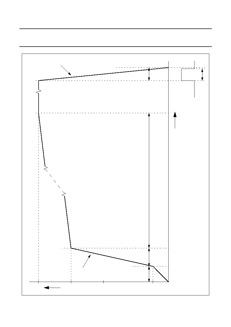
2000
Jun
22
116
Philips Semiconductors
T
entativ
e De
vice Specification
TV signal processor-T
elete
xt decoder with
embedded
µ
-Controller
TD
A955X/6X/8X PS/N1 ser
ies
T
ON
(%)
50
100
Fig. 45 Soft start and soft stop behaviour of horizontal output and timing picture tube discharge current
57
73
1045
43
38
Discharge current
picture tube
Time (ms)
Soft start
Soft stop
75
12

2000 Jun 22
117
Philips Semiconductors
Tentative Device Specification
TV signal processor-Teletext decoder with
embedded
µ
-Controller
TDA955X/6X/8X PS/N1 series
Fig.46 Timing of vertical blanking and black current measuring pulses
Reset V
e
r
t. Sa
w
V
e
r
t. Blank
Blac
k current pulses
Video
625
23
Video
312
336
Blac
k current pulses
V
e
r
t. Blank
RESET LINE COUNTER
Reset V
e
r
t. Sa
w
V
e
r
t. Blank
Blac
k current pulses
inter
nal
LR
G
B
50Hz
60Hz
1ST
2ND
1ST
2ND
signal
signal
inter
nal
FIELD
FIELD
FIELD
FIELD
2f
H
cloc
k
V
e
r
t. Blank
Blac
k current pulses
2f
H
cloc
k
LR
G
B
4.5 lines (OSVE = 0)
14.5 lines (OSVE = 1)
4.5 lines (OSVE = 0)
14.5 lines (OSVE = 1)
14 lines
17
18
19
20
329
330
331
332
end line 23 (OSVE = 0)
end line 33 (OSVE = 1)
line 335.5 (OSVE = 0)
line 345.5 (OSVE = 1)
LR
G
B
LR
G
B
17
18
19
20
279
280
281
282
end line 20(OSVE = 0)
end line 32 (OSVE = 1)
line 282.5 (OSVE = 0)
line 294.5 (OSVE = 1)
4 lines (OSVE = 0)
16 lines (OSVE = 1)
4 lines (OSVE = 0)
16 lines (OSVE = 1)
9.5 lines
2000 Jun 22
118
Philips Semiconductors
Tentative Device Specification
TV signal processor-Teletext decoder with
embedded
µ
-Controller
TDA955X/6X/8X PS/N1 series
Fig.47 Peak White Limiting / Soft clipper characteristic.
20
40
60
80
100
2.0
3.0
YIN (IRE)
clipper off
clipper on
1.0
RGBout
(V
b-w
)
PWL setting
4.0
120
130
00H
08H
0FH
Soft clipping
range
(Defined by
SOC1/SOC0 bits)
VIDEO
REF
-1
BURST KEY
BLANKING
3.5
µ
s
7.8
µ
s
5.9
µ
s
10.2
µ
s
15 steps of 0.16
µ
s
15 steps of 0.16
µ
s
Fig.48 Timing of horizontal wide blanking
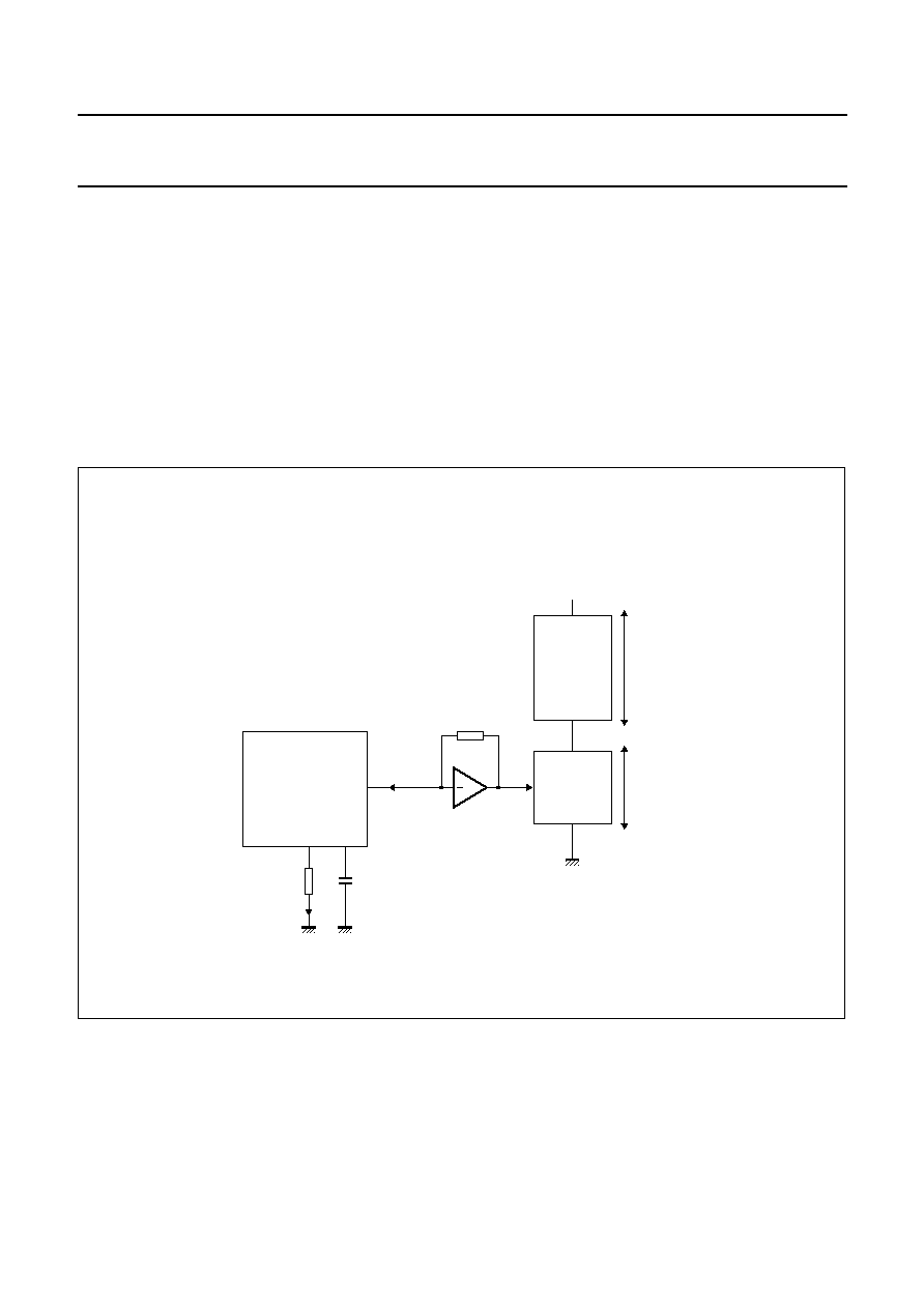
2000 Jun 22
119
Philips Semiconductors
Tentative Device Specification
TV signal processor-Teletext decoder with
embedded
µ
-Controller
TDA955X/6X/8X PS/N1 series
TEST AND APPLICATION INFORMATION
East-West output stage
In order to obtain correct tracking of the vertical and
horizontal EHT-correction, the EW output stage should be
dimensioned as illustrated in Fig.49.
Resistor R
EW
determines the gain of the EW output stage.
Resistor R
c
determines the reference current for both the
vertical sawtooth generator and the geometry processor.
The preferred value of R
c
is 39 k
which results in a
reference current of 100
µ
A (V
ref
= 3.9 V).
The value of R
EW
must be:
Example: With V
ref
= 3.9 V; R
c
= 39 k
and V
scan
= 120 V
then R
EW
= 68 k
.
R
EW
R
c
V
scan
18
V
ref
◊
-----------------------
◊
=
handbook, full pagewidth
MLA744 - 1
TDA8366
HORIZONTAL
DEFLECTION
STAGE
DIODE
MODULATOR
VDD
V scan
V EW
Rew
EW output
stage
EWD
Csaw
100 nF
(5%)
Vref
Rc
39 k
(2%)
I ref
43
49
50
Fig. 49 East-West output stage.
TDA
935X
21
28
27
UOC series
15
20
21

2000 Jun 22
120
Philips Semiconductors
Tentative Device Specification
TV signal processor-Teletext decoder with
embedded
µ
-Controller
TDA955X/6X/8X PS/N1 series
Fig. 50 Control range of vertical amplitude.
VA = 0, 1FH and 3FH; VSH = 1FH; SC = 0EH.
Fig. 51 Control range of vertical slope.
VS = 0, 1FH and 3FH; VA = 1FH; VSH = 1FH; SC = 0EH.
700
500
300
100
-100
-300
-500
-700
I
VERT
(
µ
A)
TIME
0
T/2
T
Fig. 52 Control range of vertical shift.
VSH = 0, 1FH and 3FH; VA = 1FH; SC = 0EH.
-1.0
-750.0m
-500.0m
-250.0m
0.0
250.0m
500.0m
750.0m
1.0
Fig. 53 Control range of S-correction.
SC = 0, 0EH and 3FH; VA = 1FH; VSH = 1FH.
TIME
0
T/2
T
I
VERT
(
µ
A)
600
400
200
0
-200
-400
-600
2000 Jun 22
121
Philips Semiconductors
Tentative Device Specification
TV signal processor-Teletext decoder with
embedded
µ
-Controller
TDA955X/6X/8X PS/N1 series
0.0
200.0m
400.0m
600.0m
800.0m
1.0
Fig. 54 Control range of EW width.
EW = 0, 1FH and 3FH; PW = 3FH; TC = 1FH; CP = 11H.
1200
1000
800
600
400
200
0
I
EW
(
µ
A)
0
T/2
T
TIME
0.0
200.0m
400.0m
600.0m
800.0m
1.0
Fig. 55 Control range of EW parabola/width ratio.
PW = 0, 1FH and 3FH; EW = 3FH; TC = 1FH; CP = 11H.
I
EW
(
µ
A)
0
T/2
T
TIME
500
400
300
200
100
0
0.0
200.0m
400.0m
600.0m
800.0m
1.0
Fig. 56 Control range of EW corner/parabola ratio.
CP = 0, 11H and 3FH; EW = 3FH; PW = 3FH; TC = 1FH.
0
T/2
T
TIME
I
EW
(
µ
A)
600
500
400
300
200
100
0
0.0
200.0m
400.0m
600.0m
800.0m
1.0
Fig. 57 Control range of EW trapezium correction.
TC = 0, 1FH and 3FH; EW = 1FH; PW = 1FH; CP = 11H.
I
EW
(
µ
A)
0
T/2
T
TIME
650
600
550
500
450
400
350

2000 Jun 22
122
Philips Semiconductors
Tentative Device Specification
TV signal processor-Teletext decoder with
embedded
µ
-Controller
TDA955X/6X/8X PS/N1 series
Adjustment of geometry control parameters
The deflection processor offers 5 control parameters for
picture alignment, viz:
∑
S-correction
∑
vertical amplitude
∑
vertical slope
∑
vertical shift
∑
horizontal shift.
The 110
∞
types offer in addition:
∑
EW width
∑
EW parabola width
∑
EW upper/lower corner parabola
∑
EW trapezium correction.
∑
Vertical zoom
∑
Horizontal parallelogram and bow correction for some
versions in the range
It is important to notice that the ICs are designed for use
with a DC-coupled vertical deflection stage. This is the
reason why a vertical linearity alignment is not necessary
(and therefore not available).
For a particular combination of picture tube type, vertical
output stage and EW output stage it is determined which
are the required values for the settings of S-correction, EW
parabola/width ratio and EW corner/parabola ratio. These
parameters can be preset via the I
2
C-bus, and do not need
any additional adjustment. The rest of the parameters are
preset with the mid-value of their control range (i.e. 1FH),
or with the values obtained by previous TV-set
adjustments.
The vertical shift control is meant for compensation of
off-sets in the external vertical output stage or in the
picture tube. It can be shown that without compensation
these off-sets will result in a certain linearity error,
especially with picture tubes that need large S-correction.
The total linearity error is in first order approximation
proportional to the value of the off-set, and to the square of
the S-correction needed. The necessity to use the vertical
shift alignment depends on the expected off-sets in vertical
output stage and picture tube, on the required value of the
S-correction, and on the demands upon vertical linearity.
For adjustment of the vertical shift and vertical slope
independent of each other, a special service blanking
mode can be entered by setting the SBL bit HIGH. In this
mode the RGB-outputs are blanked during the second half
of the picture. There are 2 different methods for alignment
of the picture in vertical direction. Both methods make use
of the service blanking mode.
The first method is recommended for picture tubes that
have a marking for the middle of the screen. With the
vertical shift control the last line of the visible picture is
positioned exactly in the middle of the screen. After this
adjustment the vertical shift should not be changed. The
top of the picture is placed by adjustment of the vertical
amplitude, and the bottom by adjustment of the vertical
slope.
The second method is recommended for picture tubes that
have no marking for the middle of the screen. For this
method a video signal is required in which the middle of the
picture is indicated (e.g. the white line in the circle test
pattern). With the vertical slope control the beginning of the
blanking is positioned exactly on the middle of the picture.
Then the top and bottom of the picture are placed
symmetrical with respect to the middle of the screen by
adjustment of the vertical amplitude and vertical shift.
After this adjustment the vertical shift has the right setting
and should not be changed.
If the vertical shift alignment is not required VSH should be
set to its mid-value (i.e. VSH = 1F). Then the top of the
picture is placed by adjustment of the vertical amplitude
and the bottom by adjustment of the vertical slope. After
the vertical picture alignment the picture is positioned in
the horizontal direction by adjustment of the EW width and
the horizontal shift. Finally (if necessary) the left- and
right-hand sides of the picture are aligned in parallel by
adjusting the EW trapezium control.
To obtain the full range of the vertical zoom function the
adjustment of the vertical geometry should be carried out
at a nominal setting of the zoom DAC at position 19 HEX.
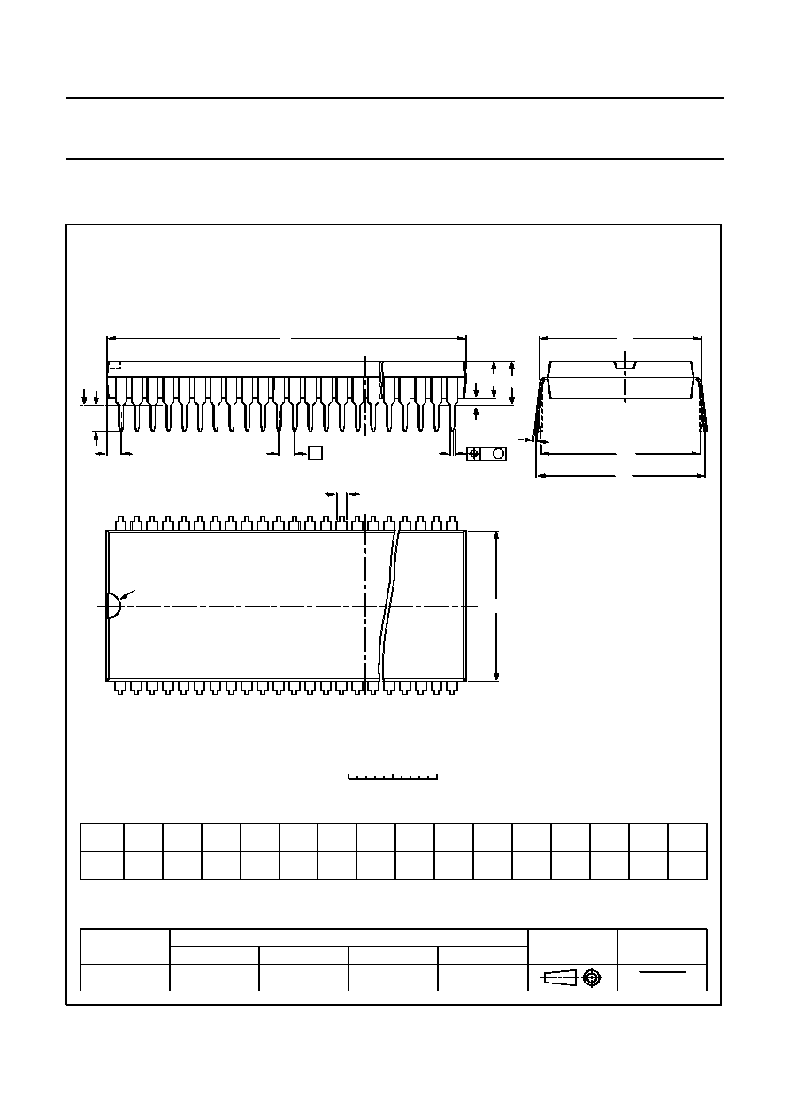
2000 Jun 22
123
Philips Semiconductors
Tentative Device Specification
TV signal processor-Teletext decoder with
embedded
µ
-Controller
TDA955X/6X/8X PS/N1 series
PACKAGE OUTLINE
UNIT
b
1
c
E
e
M
H
L
REFERENCES
OUTLINE
VERSION
EUROPEAN
PROJECTION
ISSUE DATE
IEC
JEDEC
EIAJ
mm
DIMENSIONS (mm are the original dimensions)
SOT274-1
92-10-13
95-02-04
b
max.
w
M
E
e
1
1.3
0.8
0.53
0.40
0.32
0.23
58.67
57.70
17.2
16.9
3.2
2.8
0.18
1.778
19.05
19.61
19.05
20.96
19.71
1.73
5.84
0.51
4.57
M
H
c
(e )
1
M
E
A
L
seating plane
A
1
w
M
b
1
e
D
A
2
Z
0
5
10 mm
scale
Note
1. Plastic or metal protrusions of 0.25 mm maximum per side are not included.
(1)
(1)
D
(1)
Z
64
1
33
32
b
E
pin 1 index
A
max.
1
2
A
min.
A
max.
SDIP64: plastic shrink dual in-line package; 64 leads (750 mil)
SOT274-1

2000 Jun 22
124
Philips Semiconductors
Tentative Device Specification
TV signal processor-Teletext decoder with
embedded
µ
-Controller
TDA955X/6X/8X PS/N1 series
SOLDERING
Introduction
There is no soldering method that is ideal for all IC
packages. Wave soldering is often preferred when
through-hole and surface mounted components are mixed
on one printed-circuit board. However, wave soldering is
not always suitable for surface mounted ICs, or for
printed-circuits with high population densities. In these
situations reflow soldering is often used.
This text gives a very brief insight to a complex technology.
A more in-depth account of soldering ICs can be found in
our
"IC package Databook" (order code 9398 652 90011).
SDIP
S
OLDERING BY DIPPING OR BY WAVE
The maximum permissible temperature of the solder is
260
∞
C; solder at this temperature must not be in contact
with the joint for more than 5 seconds. The total contact
time of successive solder waves must not exceed
5 seconds.
The device may be mounted up to the seating plane, but
the temperature of the plastic body must not exceed the
specified maximum storage temperature (T
stg max
). If the
printed-circuit board has been pre-heated, forced cooling
may be necessary immediately after soldering to keep the
temperature within the permissible limit.
R
EPAIRING SOLDERED JOINTS
Apply a low voltage soldering iron (less than 24 V) to the
lead(s) of the package, below the seating plane or not
more than 2 mm above it. If the temperature of the
soldering iron bit is less than 300
∞
C it may remain in
contact for up to 10 seconds. If the bit temperature is
between 300 and 400
∞
C, contact may be up to 5 seconds.
QFP
R
EFLOW SOLDERING
Reflow soldering techniques are suitable for all QFP
packages.
The choice of heating method may be influenced by larger
plastic QFP packages (44 leads, or more). If infrared or
vapour phase heating is used and the large packages are
not absolutely dry (less than 0.1% moisture content by
weight), vaporization of the small amount of moisture in
them can cause cracking of the plastic body. For details,
refer to the Drypack information in our
"Quality Reference
Handbook" (order code 9397 750 00192).
Reflow soldering requires solder paste (a suspension of
fine solder particles, flux and binding agent) to be applied
to the printed-circuit board by screen printing, stencilling or
pressure-syringe dispensing before package placement.
Several methods exist for reflowing; for example,
infrared/convection heating in a conveyor type oven.
Throughput times (preheating, soldering and cooling) vary
between 50 and 300 seconds depending on heating
method. Typical reflow peak temperatures range from
215 to 250
∞
C.
W
AVE SOLDERING
Wave soldering is not recommended for QFP packages.
This is because of the likelihood of solder bridging due to
closely-spaced leads and the possibility of incomplete
solder penetration in multi-lead devices.
If wave soldering cannot be avoided, for QFP
packages with a pitch (e) larger than 0.5 mm, the
following conditions must be observed:
∑
A double-wave (a turbulent wave with high upward
pressure followed by a smooth laminar wave)
soldering technique should be used.
∑
The footprint must be at an angle of 45
∞
to the board
direction and must incorporate solder thieves
downstream and at the side corners.
During placement and before soldering, the package must
be fixed with a droplet of adhesive. The adhesive can be
applied by screen printing, pin transfer or syringe
dispensing. The package can be soldered after the
adhesive is cured.
Maximum permissible solder temperature is 260
∞
C, and
maximum duration of package immersion in solder is
10 seconds, if cooled to less than 150
∞
C within
6 seconds. Typical dwell time is 4 seconds at 250
∞
C.
A mildly-activated flux will eliminate the need for removal
of corrosive residues in most applications.
R
EPAIRING SOLDERED JOINTS
Fix the component by first soldering two diagonally-
opposite end leads. Use only a low voltage soldering iron
(less than 24 V) applied to the flat part of the lead. Contact
time must be limited to 10 seconds at up to 300
∞
C. When
using a dedicated tool, all other leads can be soldered in
one operation within 2 to 5 seconds between
270 and 320
∞
C.

2000 Jun 22
125
Philips Semiconductors
Tentative Device Specification
TV signal processor-Teletext decoder with
embedded
µ
-Controller
TDA955X/6X/8X PS/N1 series
DEFINITIONS
LIFE SUPPORT APPLICATIONS
These products are not designed for use in life support appliances, devices, or systems where malfunction of these
products can reasonably be expected to result in personal injury. Philips customers using or selling these products for
use in such applications do so at their own risk and agree to fully indemnify Philips for any damages resulting from such
improper use or sale.
PURCHASE OF PHILIPS I
2
C COMPONENTS
Data sheet status
Objective specification
This data sheet contains target or goal specifications for product development.
Preliminary specification
This data sheet contains preliminary data; supplementary data may be published later.
Product specification
This data sheet contains final product specifications.
Limiting values
Limiting values given are in accordance with the Absolute Maximum Rating System (IEC 134). Stress above one or
more of the limiting values may cause permanent damage to the device. These are stress ratings only and operation
of the device at these or at any other conditions above those given in the Characteristics sections of the specification
is not implied. Exposure to limiting values for extended periods may affect device reliability.
Application information
Where application information is given, it is advisory and does not form part of the specification.
Purchase of Philips I
2
C components conveys a license under the Philips' I
2
C patent to use the
components in the I
2
C system provided the system conforms to the I
2
C specification defined by
Philips. This specification can be ordered using the code 9398 393 40011.