Document Outline
- CONTENTS
- 1 FEATURES
- 2 GENERAL DESCRIPTION
- 3 ORDERING INFORMATION
- 4 BLOCK DIAGRAM
- 5 PINNING
- 6 FUNCTIONAL DESCRIPTION
- 6.1 Record-mute mode or head identification selection
- 6.2 Hi-fi audio output level
- 6.3 Reference current
- 6.4 Head amplifier
- 6.5 Automatic calibration
- 6.6 Power muting
- 6.7 Envelope output
- 6.8 RF converter output
- 6.9 Audio dubbing
- 7 I 2 C-BUS PROTOCOL
- 7.1 Addresses and data bytes
- 7.2 Valid transmissions to and from the TDA9605H
- 7.3 Overview of the TDA9605H I 2 C-bus control
- 7.4 Control byte at subaddress 00H
- 7.5 Select byte at subaddress 01H
- 7.6 Input byte at subaddress 02H
- 7.7 Output byte at subaddress 03H
- 7.8 Volume bytes at subaddresses 04H, 05H and 06H
- 7.9 Power byte at subaddress 07H
- 8 LIMITING VALUES
- 9 THERMAL CHARACTERISTICS
- 10 GENERAL CHARACTERISTICS
- 11 RECORD-MUTE MODE CHARACTERISTICS
- 12 RECORD MODE CHARACTERISTICS
- 13 PLAYBACK MODE CHARACTERISTICS
- 14 APPLICATION AND TEST INFORMATION
- 14.1 RM and HID control signals
- 14.3 Setting line output level
- 14.4 Test modes
- 15 INTERNAL CIRCUITRY
- 16 PACKAGE OUTLINE
- 17 SOLDERING
- 17.1 Introduction to soldering surface mount packages
- 17.2 Reflow soldering
- 17.3 Wave soldering
- 17.4 Manual soldering
- 17.5 Suitability of surface mount IC packages for wave and reflow soldering methods
- 18 DEFINITIONS
- 19 LIFE SUPPORT APPLICATIONS
- 20 PURCHASE OF PHILIPS I 2 C COMPONENTS

DATA SHEET
Product specification
File under Integrated Circuits, IC02
1999 Apr 14
INTEGRATED CIRCUITS
TDA9605H
Audio processor with head amplifier
for VHS hi-fi

1999 Apr 14
2
Philips Semiconductors
Product specification
Audio processor with head amplifier for VHS hi-fi
TDA9605H
CONTENTS
1
FEATURES
2
GENERAL DESCRIPTION
3
ORDERING INFORMATION
4
BLOCK DIAGRAM
5
PINNING
6
FUNCTIONAL DESCRIPTION
6.1
Record-mute mode or head identification
selection
6.2
Hi-fi audio output level
6.3
Reference current
6.4
Head amplifier
6.4.1
Playback mode
6.4.2
Record-mute mode
6.4.3
Record mode
6.4.4
Head amplifier power supply and ground
6.5
Automatic calibration
6.6
Power muting
6.7
Envelope output
6.8
RF converter output
6.9
Audio dubbing
6.9.1
Output mix
6.9.2
Input mix
7
I
2
C-BUS PROTOCOL
7.1
Addresses and data bytes
7.2
Valid transmissions to and from the TDA9605H
7.3
Overview of the TDA9605H I
2
C-bus control
7.4
Control byte at subaddress 00H
7.4.1
Audio FM mode
7.4.2
Playback mode
7.4.3
Record mode
7.4.4
System standard selection
7.4.5
Head amplifier playback amplification
7.4.6
Head amplifier record current
7.5
Select byte at subaddress 01H
7.5.1
Decoder output select
7.5.2
Head amplifier record current range select
7.5.3
Normal input level
7.6
Input byte at subaddress 02H
7.6.1
Input select
7.6.2
Normal select
7.7
Output byte at subaddress 03H
7.7.1
Line output amplification
7.7.2
Output select
7.7.3
Envelope output select
7.7.4
Line output select
7.7.5
Decoder output select
7.7.6
RF converter mute
7.8
Volume bytes at subaddresses 04H, 05H
and 06H
7.8.1
Left and right volume control
7.9
Power byte at subaddress 07H
7.9.1
Calibration start
7.9.2
DC output voltage selection
7.9.3
Test mode
7.9.4
Power-on reset
7.9.5
Head amplifier disable
7.9.6
Power muting
7.9.7
Standby select
7.10
Read byte
7.10.1
Calibration ready
7.10.2
Auto-normal selection
7.10.3
Calibration error
7.10.4
Power-on reset
8
LIMITING VALUES
9
THERMAL CHARACTERISTICS
10
GENERAL CHARACTERISTICS
11
RECORD-MUTE MODE CHARACTERISTICS
12
RECORD MODE CHARACTERISTICS
13
PLAYBACK MODE CHARACTERISTICS
14
APPLICATION AND TEST INFORMATION
14.1
RM and HID control signals
14.2
Reference current resistor
14.3
Setting line output level
14.4
Test modes
15
INTERNAL CIRCUITRY
16
PACKAGE OUTLINE
17
SOLDERING
17.1
Introduction to soldering surface mount
packages
17.2
Reflow soldering
17.3
Wave soldering
17.4
Manual soldering
17.5
Suitability of surface mount IC packages for
wave and reflow soldering methods
18
DEFINITIONS
19
LIFE SUPPORT APPLICATIONS
20
PURCHASE OF PHILIPS I
2
C COMPONENTS
1999 Apr 14
3
Philips Semiconductors
Product specification
Audio processor with head amplifier for VHS hi-fi
TDA9605H
1
FEATURES
∑
All functions controlled via the serial 2-wire I
2
C-bus
∑
Integrated standby modes for low power consumption
∑
Audio FM head amplifier:
≠ Programmable recording current
≠ Programmable playback amplification
≠ Fast record-mute mode control input.
∑
Hi-fi signal processing:
≠ Adjustment free
≠ High performance
≠ Low distortion switching noise suppressor
≠ NTSC and PAL (SECAM) system.
∑
Linear audio input:
≠ Programmable (playback) level.
∑
5 stereo inputs and additional mono Second Audio
Program (SAP) input
∑
2 stereo outputs (line and decoder) with independent
output select function
∑
RF converter output with overload-protection AGC
∑
Integrated output power muting
∑
Audio level meter output
∑
Extensive input and output select function
∑
Full support of video recorder feature modes.
2
GENERAL DESCRIPTION
The TDA9605H is a single-chip device in a small package
that contains all the required functions, including the head
amplifier, to realize the audio FM hi-fi stereo system in a
VHS video recorder (see Fig.1). The device is adjustment
free by use of an integrated auto-calibration system.
Extensive signal select functions are offered to support
pay-TV decoding and video recorder feature modes.
The high performance and functionality of the TDA9605H
comprises world-wide system and application
requirements for NTSC, PAL, SECAM and multi-standard
video recorders from basic up to high-end models.
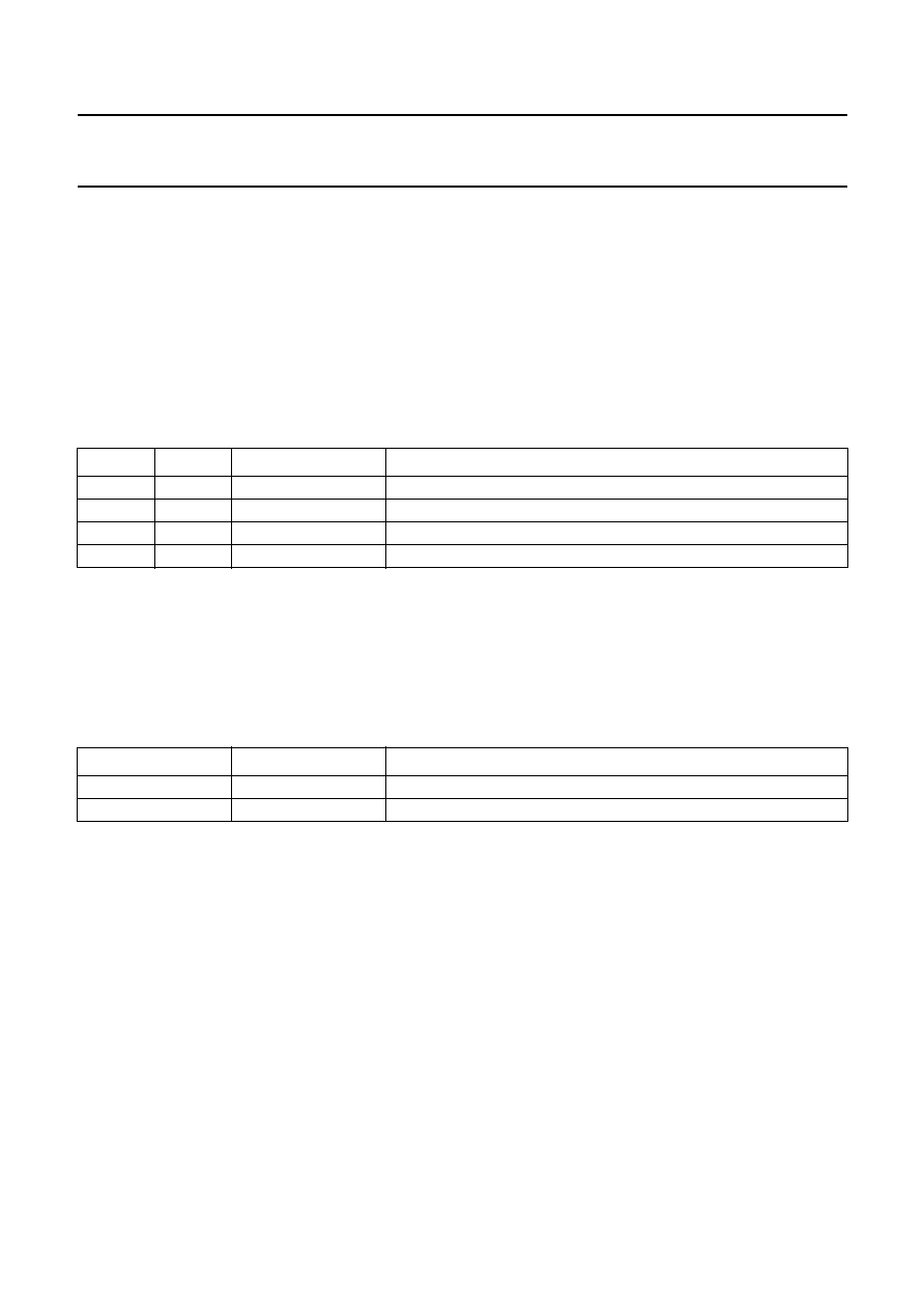
3
ORDERING INFORMATION
TYPE
NUMBER
PACKAGE
NAME
DESCRIPTION
VERSION
TDA9605H
QFP44
plastic quad flat package; 44 leads (lead length 1.3 mm);
body 10
◊
10
◊
1.75 mm
SOT307-2
1999
Apr
14
4
Philips Semiconductors
Product specification
Audio processor with head amplifier for VHS hi-fi
TDA9605H
This text is here in white to force landscape pages to be rotated correctly when browsing through the pdf in the Acrobat reader.This text is here in
_
white to force landscape pages to be rotated correctly when browsing through the pdf in the Acrobat reader.This text is here inThis text is here in
white to force landscape pages to be rotated correctly when browsing through the pdf in the Acrobat reader. white to force landscape pages to be ...
4
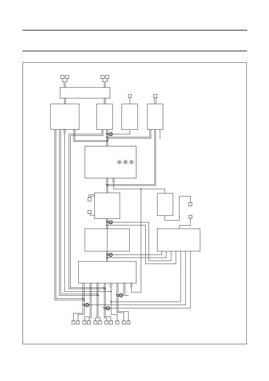
BLOCK DIAGRAM
n
dbook, full pagewidth
MGR834
M
M
M
M
TUL
SAP
VCCH
GNDH
PBIN1
PBIN2
RECOUT
HMSW
1
TUNL
2
TUNR
3
CINL
4
40
39
37
35
36
38
CINR
5
EXT1L
6
EXT1R
7
EXT2L
SAP
TUL
TUR
E1L
E1R
E2L
E2R
8
EXT2R
9
AUXL
10
AUXR
N
dub
11
normal select
input select
volume right
M
normal
input
level
RF converter
mute
volume left
decoder
select
+
1 dB 12 V
TDA9605H
1.7 or 1.8 MHz
SAP
21
22
LINOUT LININ
TUR
DCL
DCR
HID
HID
SDA
SCL
DCFBL
26
25
EMPHL
24
DCL
23
DETL
DCFBR
EMPHR
DCR
DETR
TUL
E1L
SAP
TUR
E1R
E2L
E2R
VCC
SAP
+
+
+
+
+
+
41
44
42
43
standby select
SUPPLY
VCC
GND
Vref
Iref
34
27
29
28
playback.
+
record-mute,
recording
M
+
E2L
E2R
+
HF LFP
L
DCR
R
N
dub
HF LIMITER
PEAK HOLD
LEVEL
DETECTOR
PLL
CCO
(1.7 or
1.8 MHz)
LEVEL
DETECTOR
DROPOUT
CANCELING
HI-FI
DETECTOR
1.3 or 1.4 MHz
HF LFP
HF AGC
M
carrier ratio select,
record-mute
playback head
amplification,
record head
current
HF LIMITER
PLL
CCO
(1.3 or
1.4 MHz)
envelope output
select
+
record
envelope
output
select
+
playback
DCL
MUTEL
MUTER
LINEL
DECR
DECL
LINER
RFCOUT
MUTEC
mute
R
L
PEAK HOLD
AUTO-MUTE
line select
output select
AUTN
AUTN
M
NOISE
SUPPRESSION
NOISE
SUPPRESSION
RECTIFIER
NOISE REDUCTION
FM (DE-)MODULATOR
HEAD AMPLIFIER
I/O CONTROL
CCA
W
+
FM
5th ORDER
AUDIO LPF
COMPRESSOR
EXPANDER
DETECTOR
AUDIO
CLIPPER
I
2
C-BUS
INTERFACE
M = mute
I
2
C-bus
control
HID
RM
RMHID
ENVOUT
RM
19
20
16
15
17
18
13
14
AUDIO
CLIPPER
12
RFCAGC
30
31
32
33
RECTIFIER
CCA
W
+
FM
5th ORDER
AUDIO LPF
COMPRESSOR
EXPANDER
DETECTOR
Fig.1 Block diagram.
1999 Apr 14
5
Philips Semiconductors
Product specification
Audio processor with head amplifier for VHS hi-fi
TDA9605H
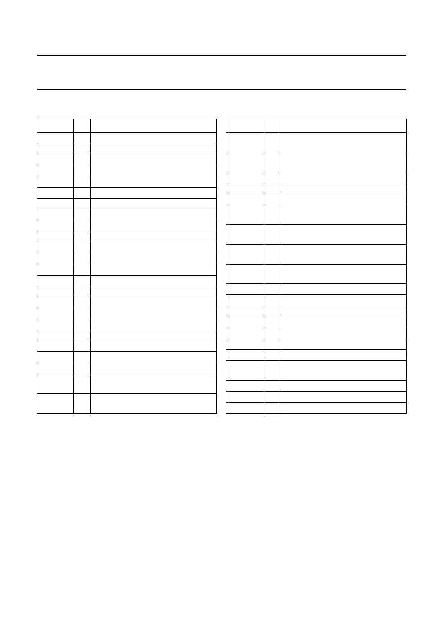
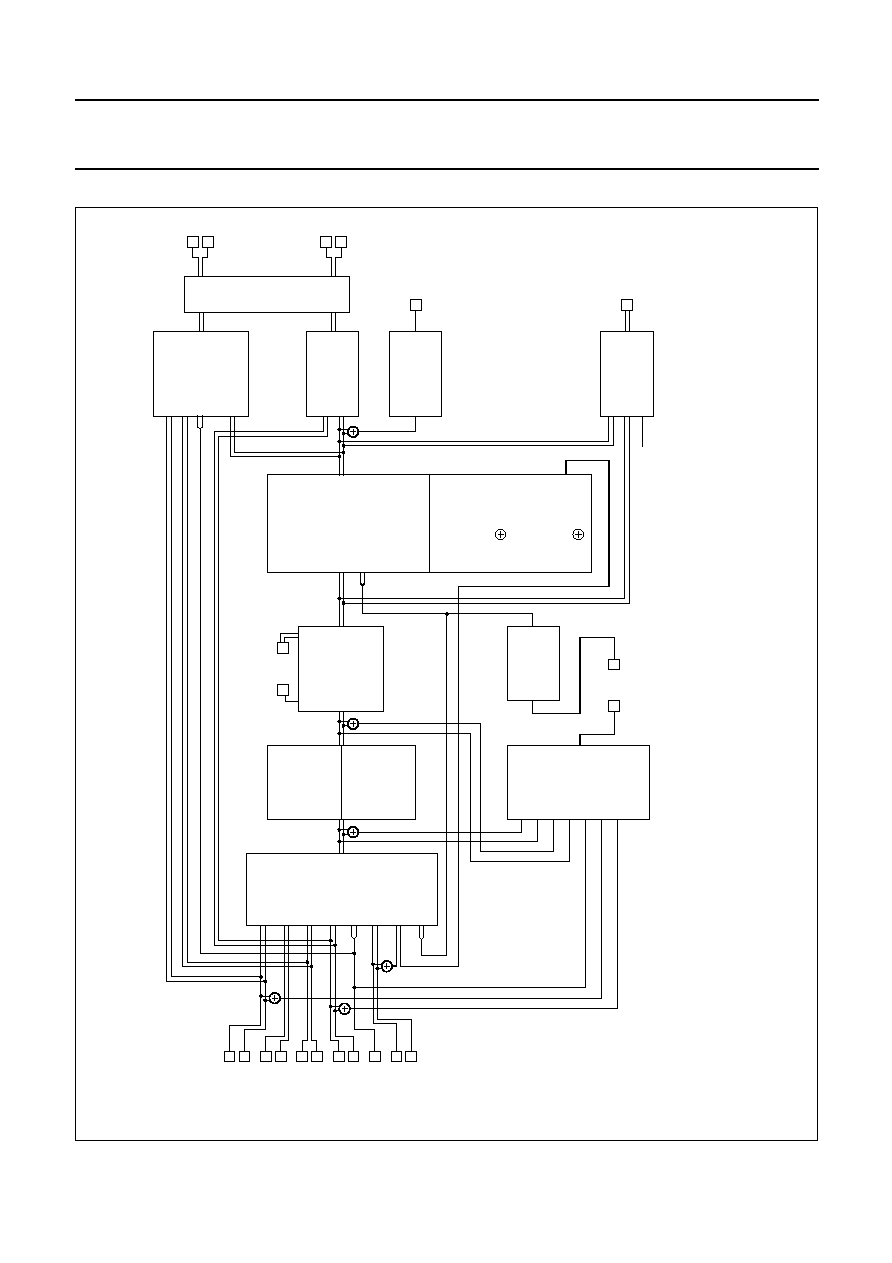
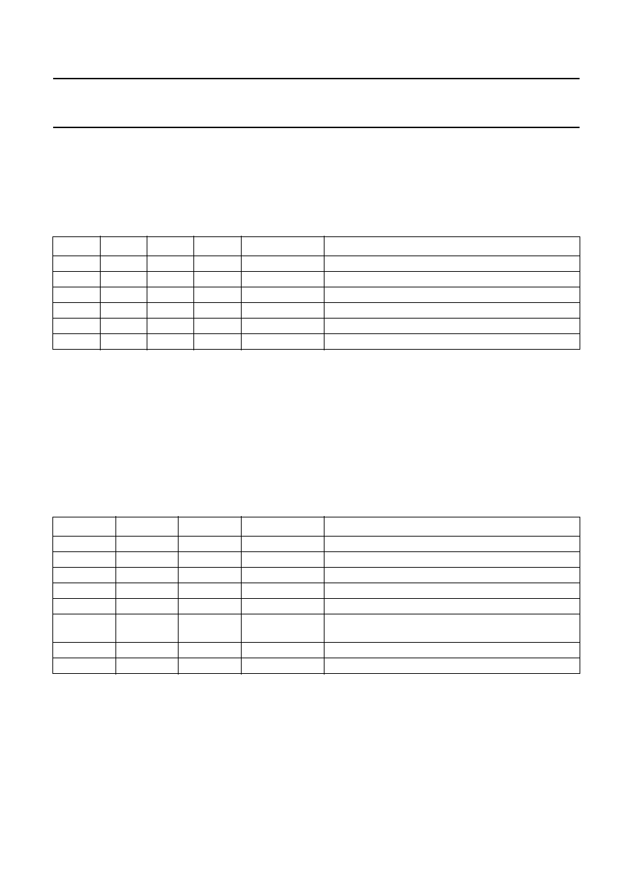
5
PINNING
SYMBOL PIN
DESCRIPTION
SAP
1
tuner input mono
TUNL
2
tuner input left
TUNR
3
tuner input right
CINL
4
CINCH input left
CINR
5
CINCH input right
EXT1L
6
external 1 input left
EXT1R
7
external 1 input right
EXT2L
8
external 2 input left
EXT2R
9
external 2 input right
AUXL
10
auxiliary input left
AUXR
11
auxiliary input right
RFCAGC
12
RF converter AGC timing connection
RFCOUT
13
RF converter output
MUTEC
14
mute for RF converter output
MUTEL
15
mute for line output left
LINEL
16
line output left
LINER
17
line output right
MUTER
18
mute for line output right
DECL
19
decoder output left
DECR
20
decoder output right
LINOUT
21
linear audio output
LININ
22
linear audio input
DCFBL
23
DC feedback noise reduction
connection left
EMPHL
24
emphasis noise reduction connection
left
DCL
25
DC decoupling noise reduction
connection left
DETL
26
detector noise reduction connection
left
GND
27
ground
I
ref
28
reference standard current connection
V
ref
29
reference voltage connection
DETR
30
detector noise reduction connection
right
DCR
31
DC decoupling noise reduction
connection right
EMPHR
32
emphasis noise reduction connection
right
DCFBR
33
DC feedback noise reduction
connection right
V
CC
34
power supply
PBIN2
35
head 2 playback input
RECOUT
36
recording current output
PBIN1
37
head 1 playback input
HMSW
38
head amplifier mode switch connection
GNDH
39
ground of head amplifier
V
CCH
40
power supply of head amplifier
RMHID
41
record-mute mode or head
identification input
SDA
42
I
2
C-bus data input/output
SCL
43
I
2
C-bus clock input
ENVOUT
44
HF or AF envelope output
SYMBOL PIN
DESCRIPTION
1999 Apr 14
6
Philips Semiconductors
Product specification
Audio processor with head amplifier for VHS hi-fi
TDA9605H
6
FUNCTIONAL DESCRIPTION
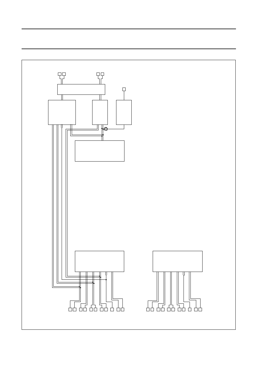
Input and output selections for the various modes are given in the following diagrams:
∑
Standard operating mode (see Fig.3)
∑
Dub-mix mode (see Fig.4)
∑
Standby mode: active or passive (see Fig.5).
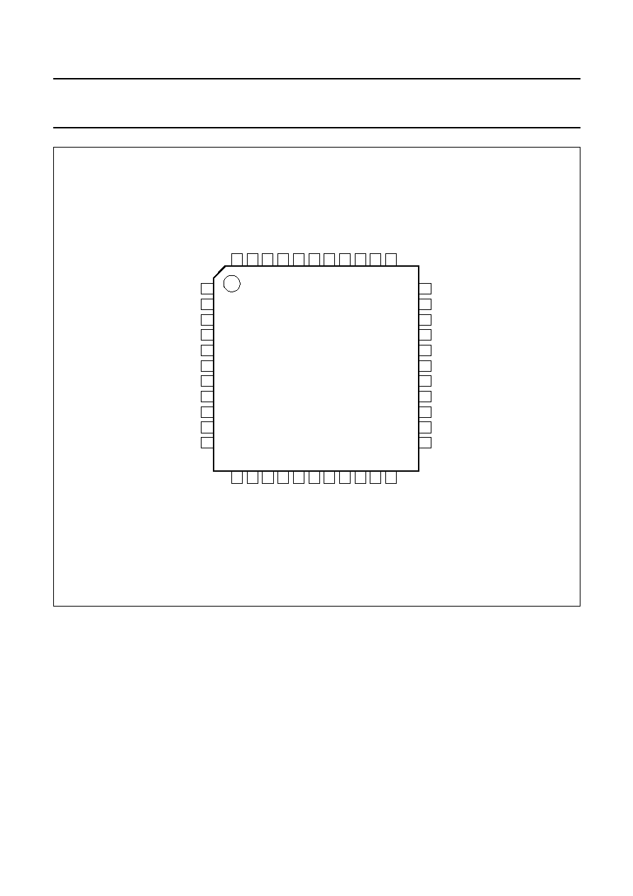
Fig.2 Pin configuration.
handbook, full pagewidth
1
2
3
4
5
6
7
8
9
10
11
33
32
31
30
29
28
27
26
25
24
23
12
13
14
15
16
17
18
19
20
21
22
44
43
42
41
40
39
38
37
36
35
34
TDA9605H
MGR835
DCFBR
EMPHR
DCR
DETR
Iref
GND
DETL
DCL
EMPHL
DCFBL
SAP
TUNL
TUNR
CINL
CINR
EXT1L
EXT2L
EXT2R
AUXR
Vref
SCL
SDA
RMHID
V
CCH
GNDH
HMSW
RECOUT
PBIN2
V
CC
ENVOUT
PBIN1
RFCOUT
MUTEC
MUTEL
LINEL
LINER
MUTER
DECR
LINOUT
LININ
RFCAGC
DECL
EXT1R
AUXL
1999
Apr
14
7
Philips Semiconductors
Product specification
Audio processor with head amplifier for VHS hi-fi
TDA9605H
This text is here in white to force landscape pages to be rotated correctly when browsing through the pdf in the Acrobat reader.This text is here in
_
white to force landscape pages to be rotated correctly when browsing through the pdf in the Acrobat reader.This text is here inThis text is here in
white to force landscape pages to be rotated correctly when browsing through the pdf in the Acrobat reader. white to force landscape pages to be ...
o
ok, full pagewidth
MGR836
TUNL
TUNER
MUTE
(
-
47 to 0 dB;
0 to
+
15 dB)
MUTE
(0 to
+
14 dB)
AUDIO FM
PROCESSING
HI-FI
MUTE
(
-
47 to 0 dB;
0 to
+
15 dB)
CINCH
EXT1
EXT2
SAP
(1)
AUX
INPUT SELECT
INPUT LEFT
VOLUME
VOLUME LEFT
SAP
LINOUT
linear audio
processing
LININ
TUNER
EXT2
MUTE
DUB MIX
MUTE
LEFT
EXT2
OUTPUT SELECT
OUTPUT SELECT
ENVOUT
RFCOUT
HF ENVELOPE
HF envelope
STEREO
RIGHT
STEREO
NORMAL
TUNER
EXT1
SAP
MUTE
OUTPUT SELECT
NORMAL
TUNR
CINL
CINR
EXT1L
EXT1R
EXT2R
AUXL
SAP
EXT2L
AUXR
volume left
volume right
output select
line select
input select
NORMAL
LEFT
NORMAL
RIGHT
NORMAL
STEREO
decoder select
0 dB AGC
0 dB
+
1 dB
MUTE
RF converter AGC
envelope select
normal input level
normal select
DECL
line output
amplification
DECR
LINEL
LINER
RECOUT
tape
PBIN1
PBIN2
Fig.3 Input and output selections for standard operating mode.
(1) For dub-mix mode signal selections see Fig.4.
1999
Apr
14
8
Philips Semiconductors
Product specification
Audio processor with head amplifier for VHS hi-fi
TDA9605H
This text is here in white to force landscape pages to be rotated correctly when browsing through the pdf in the Acrobat reader.This text is here in
_
white to force landscape pages to be rotated correctly when browsing through the pdf in the Acrobat reader.This text is here inThis text is here in
white to force landscape pages to be rotated correctly when browsing through the pdf in the Acrobat reader. white to force landscape pages to be ...
k
, full pagewidth
MGR837
TUNL
MUTE
(
-
47 to 0 dB;
0 to
+
15 dB)
MUTE
(0 to
+
14 dB)
AUDIO FM
PROCESSING
HI-FI
MUTE
(
-
47 to 0 dB;
0 to
+
15 dB)
INPUT SELECT
INPUT LEFT
VOLUME
VOLUME LEFT
SAP
LINOUT
linear audio
processing
(record)
LININ
TUNER
EXT2
MUTE
DUB MIX
MUTE
LEFT
EXT2
OUTPUT SELECT
OUTPUT SELECT
ENVOUT
RFCOUT
HF ENVELOPE
HF envelope
STEREO
RIGHT
STEREO
NORMAL
TUNER
EXT1
SAP
MUTE
OUTPUT SELECT
TUNR
CINL
CINR
EXT1L
EXT1R
EXT2R
AUXL
SAP
EXT2L
AUXR
RECOUT
tape
volume aux
output select
line select
input select
PBIN1
PBIN2
NORMAL
NORMAL
NORMAL
MUTE
LEFT
RIGHT
MUTE
LEFT
RIGHT
LEFT
RIGHT
LEFT
RIGHT
decoder select
0 dB AGC
0 dB
+
1 dB
MUTE
RF converter AGC
envelope select
normal input level
normal select
DECL
line output
amplification
DECR
LINEL
LINER
volume hi-fi
(playback)
Fig.4 Input and output selections for dub-mix mode.
Dub-mix mode: IS2 = 1, IS1 = 0 and IS0 = 1.
Input mixing of the hi-fi (playback) signal with the auxiliary, used for linear audio dubbing recording.
Selections generally used in combination with dub-mix mode are shown in heavy line type.
1999
Apr
14
9
Philips Semiconductors
Product specification
Audio processor with head amplifier for VHS hi-fi
TDA9605H
This text is here in white to force landscape pages to be rotated correctly when browsing through the pdf in the Acrobat reader.This text is here in
_
white to force landscape pages to be rotated correctly when browsing through the pdf in the Acrobat reader.This text is here inThis text is here in
white to force landscape pages to be rotated correctly when browsing through the pdf in the Acrobat reader. white to force landscape pages to be ...
handbook, full pagewidth
MGR838
TUNL
MUTE
EXT2
OUTPUT SELECT
RFCOUT
TUNER
EXT1
SAP
MUTE
OUTPUT SELECT
TUNR
CINL
CINR
EXT1L
EXT1R
EXT2R
AUXL
SAP
EXT2L
AUXR
line select
input select
MUTE
output select
TUNL
MUTE
TUNR
CINL
CINR
EXT1L
EXT1R
EXT2R
AUXL
SAP
EXT2L
AUXR
input select
decoder select
0 dB
+
1 dB
MUTE
RF converter AGC
DECL
line output
amplification
DECR
LINEL
LINER
Fig.5 Input and output selections for standby modes.
b. Passive standby mode (bit STBP = 1); over 90% power reduction.
a. Active standby mode (bit STBA = 1, bit STBP = 0); over 80% power reduction.

1999 Apr 14
10
Philips Semiconductors
Product specification
Audio processor with head amplifier for VHS hi-fi
TDA9605H
6.1
Record-mute mode or head identification
selection
Pin RMHID allows input of two independent digital control
signals for selecting the record-mute or head identification
modes which are voltage coded. The RM control signal is
selected via a 10 k
resistor and the HID control signal is
selected via a 18 k
resistor. This set-up enables the two
signals within the TDA9605H to be separated. The RM
control signal is only in use during the record mode
(bit AFM = 1); during the playback mode (bit AFM = 0) the
RM signal is ignored. Pin RMHID should be connected to
ground when the RM control signal is not used.
The use of the RM control signal is optional since the same
function is available via the I
2
C-bus control in the
record-mute mode. However, accurate timing of recording
start and stop may sometimes be difficult to realize via the
I
2
C-bus control. In this event the RM control signal can be
used instead. There is also the possibility to use the
record-mute mode control line of the video head amplifier.
6.2
Hi-fi audio output level
When the application circuit is used in accordance with the
application diagram, the standard FM deviation of 50 kHz
equals a 1 kHz audio signal of
-
8 dBV line output level
(bit LOH = 0). A different standard audio level can be
selected by changing the external filter components of the
noise reduction on pins EMPHL and EMPHR
(see Section 14.3). The standard audio level changes
proportionally to the impedance of the external
de-emphasis filter.
6.3
Reference current
The external resistor connected to pin I
ref
defines the
internal reference currents and determines the
temperature stability of circuits adjusted by the
auto-calibration function.
6.4
Head amplifier
6.4.1
P
LAYBACK MODE
The playback mode is selected by setting bit AFM = 0.
During the playback mode the input circuit on pins PBIN2
and PBIN1 is enabled (see Fig.6). Pin RECOUT is
disabled and pin HMSW shows a low impedance to
ground, so realizing an AC ground for the head circuit via
the external capacitor connected between these pins.
The head identification (HID) signal on pin RMHID selects
between the head signals on pins PBIN2 or PBIN1. Head
selection is defined as shown in Table 1.
The state of the RM control signal on pin RMHID is don't
care in the playback mode.
I
2
C-bus control bits HAC2, HAC1 and HAC0 offer a wide
selection of playback amplification to fit different head and
head transformer specifications. The advised setting of the
playback amplification realizes a level of 24 mV (RMS) for
each carrier signal after the head amplifier to obtain a
17 dB overhead compared to the auto-normal level (hi-fi
detection). However, performance is not critical and a
different setting can be used if desired.
The carrier level can be measured using the HF envelope
output voltage on pin ENVOUT (bit EOS = 1). During
standard operating mode the HF envelope signal is
derived from the left channel carrier amplitude
(1.3 or 1.4 MHz carrier) but the special test 10 of the test
mode also enables the HF envelope output of the right
channel carrier amplitude (1.7 or 1.8 MHz carrier).
The advised carrier playback level of 24 mV (RMS) equals
an HF envelope voltage of 3.3 V.
The head amplifier output signal can be monitored directly
by using test 8 of the test mode. Pin ENVOUT functions as
the test output showing 6 dB attenuation compared to the
actual head amplifier output level (see Section 14.4).
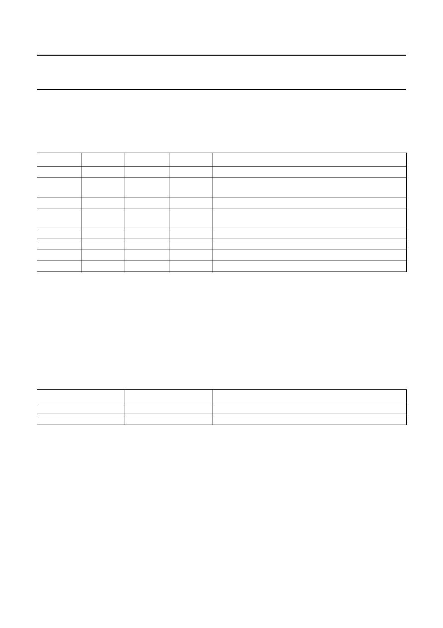
Table 1
Selection of the head signal
6.4.2
R
ECORD
-
MUTE MODE
The record-mute mode is selected by setting bit AFM = 1
and either setting bits DOC, SHH and DETH to logic 0 or
switching the RM control signal to HIGH-level.
During the record-mute mode no recording current is
present on pin RECOUT (see Fig.6). The head amplifier
status actually equals the playback mode, however, the
second amplifier stage is disabled to minimize power
consumption.
The RM control signal on pin RMHID enables fast
switching between the record and record-mute modes
(see Table 2). If the I
2
C-bus control is set to the record
mode, the use of record-mute mode control via pin RM
allows for accurate timing of recording start and stop,
independent of the I
2
C-bus control (see Section 6.1).
HID
SIGNAL
LEVEL ON PIN RMHID
SELECTION OF
HEAD SIGNAL
LOW
lower than 0.6 V or
between 2.65 and 3.8 V
pin PBIN2
(head 2)
HIGH
between 1.0 and 2.35 V
or higher than 4.3 V
pin PBIN1
(head 1)
1999 Apr 14
11
Philips Semiconductors
Product specification
Audio processor with head amplifier for VHS hi-fi
TDA9605H
Table 2
Selection of recording modes
6.4.3
R
ECORD MODE
The record mode is selected by setting bit AFM = 1 and
setting bits DOC, SHH and DETH from logic 001 to 111
and switching the RM control signal to LOW-level.
During the record mode actual recording is activated and
the recording current is output on pin RECOUT
(see Fig.6). Pins PBIN2 and PBIN1 form a connection to
the 5 V head amplifier supply voltage (V
CCH
). Pin HMSW
is internally connected to pin RECOUT and the external
capacitor has no function in this mode.
The desired carrier mix ratio is set via I
2
C-bus control
bits DOC, SHH and DETH. A wide selection of recording
currents is available to fit different head and head
transformer specifications and are set via bits HAC2,
HAC1, HAC0 and range bit HRL. The setting of the carrier
mix ratio does not change the selected recording current.
RM
SIGNAL
LEVEL ON
PIN RMHID
RECORD MODE
LOW
lower than 2.35 V
record or record-mute
mode as defined by
I
2
C-bus control
HIGH
higher than 2.65 V record-mute mode
The DC bias current on pin RECOUT is changed
proportional to the selected recording current for
optimizing the performance and minimizing the power
consumption for each recording current selected.
A Boucherot damping circuit is connected between
pin HMSW and ground to prevent head current resonance
peaking. A capacitor of 10 nF and a resistor of 470
are
specified in Fig.14, but the component values are not
critical.
6.4.4
H
EAD AMPLIFIER POWER SUPPLY AND GROUND
The head amplifier is supplied via a separate 5 V supply
(pin V
CCH
) and ground (pin GNDH).
A capacitor of 100 nF should be placed close to the device
between pins V
CCH
and GNDH for proper decoupling of
the power supply.
The head amplifier ground (pin GNDH) should be
connected to the main ground (pin GND).
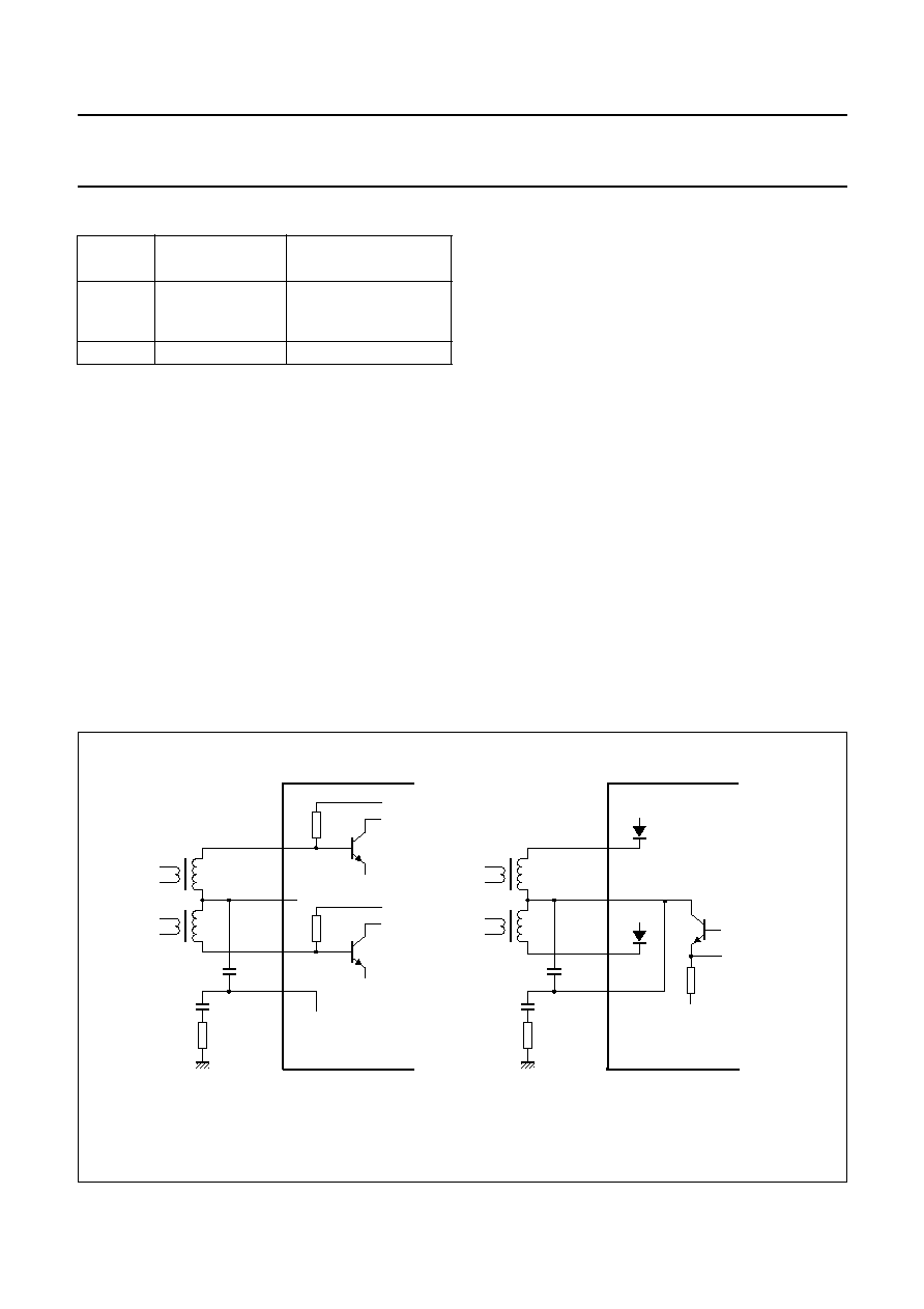
Fig.6 Simplified circuit diagrams of the head amplifier modes.
handbook, full pagewidth
MGR841
35 k
GNDH
GNDH
AH2
PBIN2
PBIN1
HMSW
RECOUT
AH1
35 k
GNDH
TDA9605H
38
37
36
35
PBIN2
PBIN1
HMSW
RECOUT
38
37
36
35
5
GNDH
AH2
AH1
VCCH
VCCH
TDA9605H
a. Playback mode and record-mute mode.
b. Record mode.
1999 Apr 14
12
Philips Semiconductors
Product specification
Audio processor with head amplifier for VHS hi-fi
TDA9605H
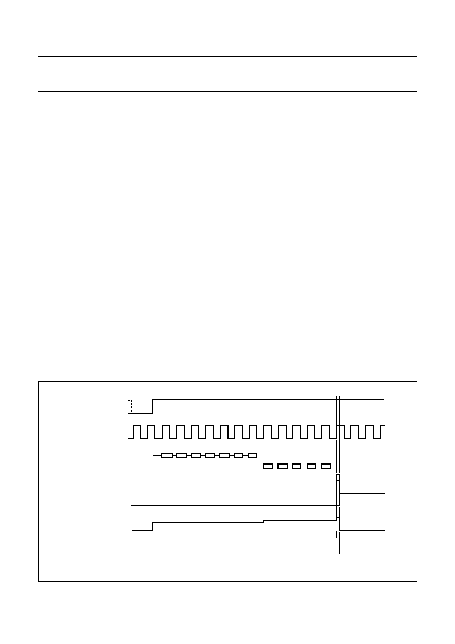
6.5
Automatic calibration
The integrated auto-calibration system is activated by
means of bit CALS of the power byte (see Fig.7).
The auto-calibration system ensures hi-fi processing is
well in accordance with the VHS hi-fi system standard by
an automated adjustment of carrier frequencies,
band-pass filters and noise reduction filters. Calibration is
only needed after start-up of the video recorder.
The calibration settings remain stable as long as the
supply voltage (V
CC
) is present.
Auto-calibration is only executed in the record-mute mode
or record mode and no standby mode or test mode should
be selected, i.e. auto-calibration requires the setting of
bit AFM = 1, bit STBP = 0, bit STBA = 0 and bit TEST = 0.
Auto-calibration is started after setting bit CALS = 1.
Calibration is performed fully automatically, using the HID
control signal as a time reference. Audio signals are not
disturbed during the calibration process.
Calibration of the oscillator frequencies is performed by
measuring the number of oscillator cycles within one
period when the HID control signal is at HIGH-level and
comparing this result with an internal value stored in the
Read Only Memory (ROM). Four different ROM values are
available for NTSC or PAL (SECAM) system calibration of
both the left and right channel carrier.
In case of NTSC a special routine is active for the
calibration of the right channel carrier which results in a
frequency difference between the left and right channel
carrier near to 401.2 kHz. This value effectively reduces
the crosstalk from hi-fi carriers to video colour signal as
present during Extended Play (EP) tape speed. NTSC
calibration uses a standard HID control signal of 29.97 Hz
(pulse width =16.683 ms) where PAL calibration uses a
standard HID control signal of 25 Hz (pulse
width = 20 ms). After auto-calibration the maximum
frequency error is
±
5 kHz assuming a time error of
maximum of 5
µ
s when the HID control signal is at
HIGH-level. Jitter on the HID control signal should not
exceed 1
µ
s to realize EP optimization within
±
2 kHz for
NTSC. In general, the crystal based HID control signal
available in the video recorder can be used without
modification.
When the calibration of the oscillators is completed the
band-pass filters are calibrated. The integrated weighting
and FM de-emphasis filters of the noise reduction are
calibrated at the same time.
The total auto-calibration time needed is maximum
17 cycles of the HID control signal. Completion of the
calibration is signalled by bit CALR =1 of the read byte.
The calibration can also be monitored by means of the
envelope output. For this purpose the voltage on
pin ENVOUT is forced to >2.5 V during the calibration.
The audio signal to the audio envelope function (level
meter) should be muted (i.e. output select = mute).
Fig.7 Example of automatic calibration flow.
handbook, full pagewidth
MGR842
logic 1
logic 0
logic 1
logic 0
4 V
3 V
5 V
calibration
ready
I
2
C-bus write bit CALS
I
2
C-bus read bit CALR
ENVOUT output
RMHD input
left channel oscillator
right channel oscillator
band-pass and
noise reduction filters
1999 Apr 14
13
Philips Semiconductors
Product specification
Audio processor with head amplifier for VHS hi-fi
TDA9605H
Otherwise, the audio envelope output voltage may
become >2.5 V which makes it impossible to detect the
completion of the calibration on pin ENVOUT.
Calibration relies upon the frequency accuracy of the HID
control signal. The calibration result may be incorrect
when the HID control signal is disturbed during a critical
part of the calibration. An additional check is incorporated
to detect such a situation by reading bit CALE during
calibration. When bit CALE = 1, the calibration result is
detected to be unreliable due to external causes. A new
auto-calibration can be started by setting bit CALS = 0
followed by setting bit CALS = 1. Bit CALE always reads
logic 1 when bit CALS is logic 0.
The oscillators and band-pass filters can be switched
between NTSC and PAL system frequencies after a
calibration in NTSC or PAL mode without the need of
additional calibration. Switching between these system
modes is executed immediately and can be done in any
operating mode. The frequency accuracy of system
switching is 100
±
3 kHz for both carriers. To obtain the
best possible frequency accuracy in the record mode it is
good practice to recalibrate after system switching.
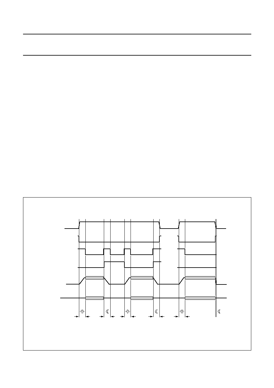
6.6
Power muting
Switching off and on of the power supply voltage or using
the built-in passive standby mode results in rising and
dropping of the output DC voltages and causes strong
disturbances on the output pins. The TDA9605H includes
three integrated mute switches to block such disturbances
so avoiding the need for an external mute circuit. Pop-free
line and RF converter output signals are realized by
connecting the integrated power mute switches behind the
line and RFC output capacitors.
Power muting is active when bit MUTE = 1 (see Fig.8).
Power muting is automatically activated when V
CC
is
switched on, because this situation is the Power-on reset
default state. The integrated mute switches on
pins MUTEC, MUTEL and MUTER are closed and form a
low-impedance path to ground. Furthermore, the
pins RFCOUT, LINEL and LINER are current limited to
-
1 mA to avoid excessive supply currents and to achieve
good noise attenuation without the need for a series
resistor between the output and mute pins. Pins DECL and
DECR are also current limited for using the integrated
power mute switches or for assisting external muting.
Fig.8 Examples of power mute control and the auto-mute function.
handbook, full pagewidth
MGR843
VCC
auto-mute
(VCC < 7 V)
bit MUTE (I
2
C-bus)
(
1
)
(
1
)
bit STBP (I
2
C-bus)
MUTEC
MUTEL
MUTER
RFCOUT
LINEL
LINER
output signal
with power mute
tmute
tmute
tmute
tmute
tmute
auto-mute
active
operation
power
off
power
off
active
operation
power off
(standby)
active
operation
passive
standby
(1) Power-on reset.

1999 Apr 14
14
Philips Semiconductors
Product specification
Audio processor with head amplifier for VHS hi-fi
TDA9605H
During power muting the internal output signal is also
muted. After the output DC voltage has been established
power muting can be de-activated by setting bit MUTE = 0.
Now the mute switches are opened resulting in a
high-impedance path of 100 k
to ground. The output
current limiting is not active.
Power muting is also used in combination with the
integrated passive standby mode (bit STBP = 1). During
this mode the output circuits are switched off and the line,
decoder and RF converter output voltages decrease to 0 V
using a discharge current of 1 mA. Do not set power mute
mode and change the passive standby mode at the same
time. Power mute mode should be activated first, followed
by switching on or off of the passive standby mode to avoid
possible output glitches.
It should be noted that the time needed for stabilizing the
output DC voltage is proportional to the output capacitor
value. A safe mute time is 200 ms using a 10
µ
F capacitor
(t
mute
= C
◊
20000 s). Power muting consumes
approximately 4 mA additional supply current, so to obtain
minimum power consumption the mute mode should be
de-activated after use. Very good performance is achieved
for power-up, power-down and passive standby mode
switching.
An auto-mute function is included which activates power
muting when the supply voltage drops below 7 V.
The performance of this auto-mute function depends upon
the power voltage drop rate. The voltage drop rate should
not exceed 1 V during 10 ms. The best performance
independent of voltage drop rate is realized by activating
the passive standby mode before switching off the power
supply voltage (by setting bit MUTE = 1 and bit STBP = 1).
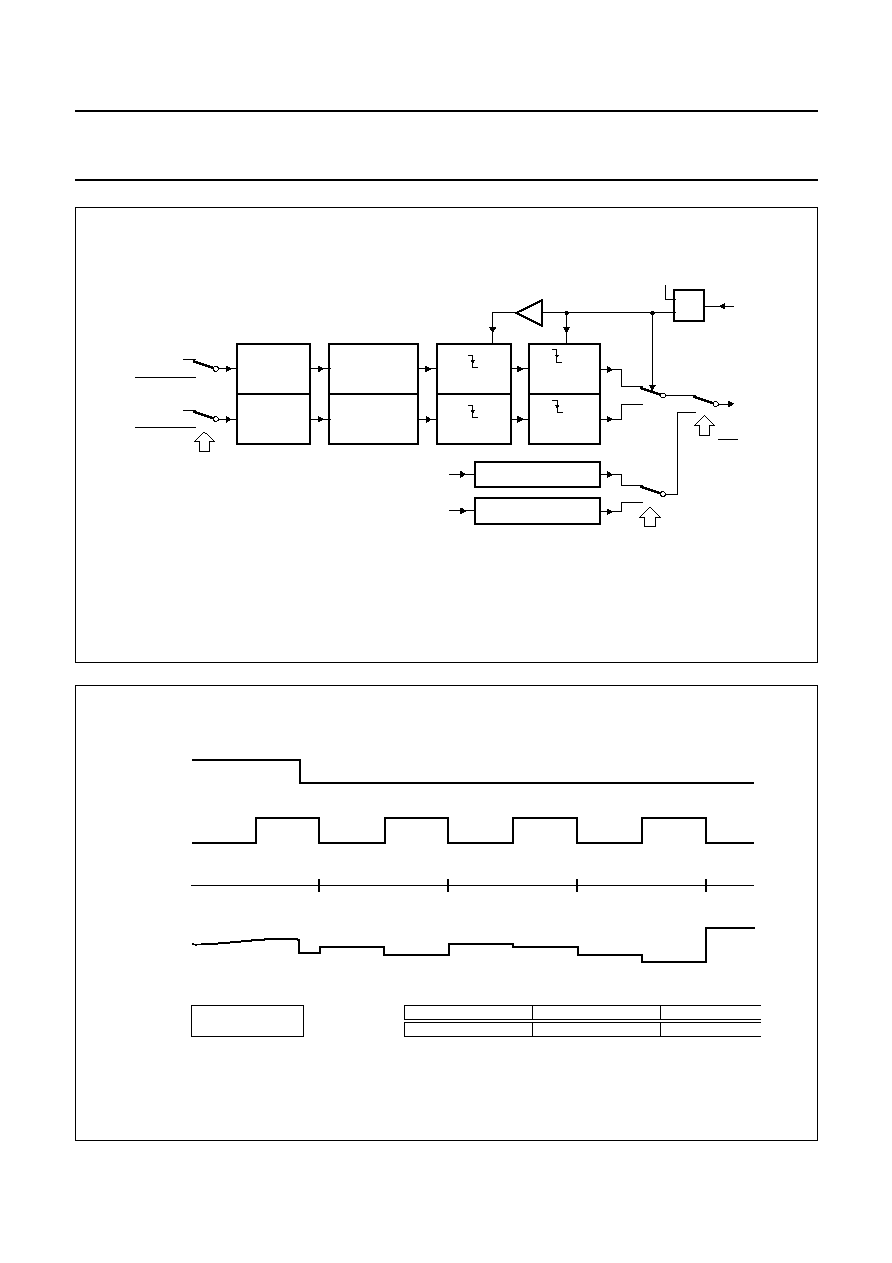
6.7
Envelope output
Pin ENVOUT is an analog output for stereo audio level
(e.g. level meter display) and for playback FM carrier level
(e.g. auto-tracking). The functional diagram is given in
Fig.9 and the timing diagram is shown in Fig.10. Only one
ADC input is needed on the microcontroller for reading all
the required information.
During the playback mode the selection between audio
level and carrier level information is realized by setting
I
2
C-bus control bit EOS (see Table 3). The AF envelope
output is defined by the signal selection made at the output
select.
During the record mode bit EOS offers the selection
between the audio level of the output select or the audio
level of the fixed hi-fi stereo signal. This is a helpful setting
when the microcontroller uses the audio level information
to adjust the hi-fi recording level (volume control).
The HF envelope output signal is continuous and is
derived from the left channel carrier. The HF envelope
output exhibits a logarithmic characteristic (see Fig.11).
In a standard application circuit only the left channel carrier
level is required to support auto-tracking or manual
tracking. However, test 10 of the special test mode allows
for the right channel carrier level output instead for
measurement purposes (see Section 14.4).
The AF envelope output as a function of the output level is
given in Fig.12.
The AF envelope circuit uses time multiplexing for the left
and right channel audio level. A peak-hold function and
dynamic range compression (square root function) are
included for easy read out. The peak-hold function and the
left and right channel multiplexing are controlled by the
HID control signal on pin RMHID (see Table 4).
Table 3
Selection of the envelope output
Table 4
AF envelope output with channel multiplexing
MODE
BIT AFM
BIT EOS
ENVELOPE OUTPUT
FUNCTION
Playback
0
0
AF envelope: via output select
level meter display
1
HF envelope
auto-tracking or manual tracking display
Record
1
0
AF envelope: via output select
level meter display
1
AF envelope: hi-fi stereo
record volume control (and level display)
HID SIGNAL
LEVEL ON PIN RMHID
AF ENVELOPE OUTPUT
LOW
lower than 0.6 V or between 2.65 and 3.8 V
left channel audio peak level
HIGH
between 1.0 and 2.35 V or higher than 4.3 V
right channel audio peak level
1999 Apr 14
15
Philips Semiconductors
Product specification
Audio processor with head amplifier for VHS hi-fi
TDA9605H
Fig.9 Functional diagram of the envelope output circuit.
handbook, full pagewidth
MGR845
output select
hi-fi
output select
left channel audio:
right channel audio:
hi-fi
EOS ∑ AFM
AF
envelope
FULL-WAVE
RECTIFIER
FULL-WAVE
RECTIFIER
PEAK HOLD
PEAK HOLD
1.3 or 1.4 MHz carrier
RESET
RESET
EOS ∑ AFM
test 10
HF
envelope
SAMPLE-
AND-HOLD
RMHID
RM
HID
ENVOUT
SAMPLE-
AND-HOLD
SAMPLE
SAMPLE
HF LEVEL DETECTOR
1.7 or 1.8 MHz carrier
HF LEVEL DETECTOR
SQUARE ROOT
COMPRESSION
SQUARE ROOT
COMPRESSION
td
Fig.10 Timing diagram of the envelope output signal.
handbook, full pagewidth
MGR844
I
2
C-bus
registers
HID signal
HID period
ENVOUT
level meter
display
EOS = 0 or AFM = 1
EOS = 1 and
AFM = 0
0
1
2
3
HF envelope
peak right
in period
-
1
peak right
in period 0
peak right
in period
+
1
peak right
in period
+
2
peak left
in period 0
left (period 0)
right (period 0)
tracking level
indication
peak left
in period 1
peak left
in period 2
peak left
in period
+
3
left (period 1)
right (period 1)
left (period 2)
right (period 2)
1999 Apr 14
16
Philips Semiconductors
Product specification
Audio processor with head amplifier for VHS hi-fi
TDA9605H
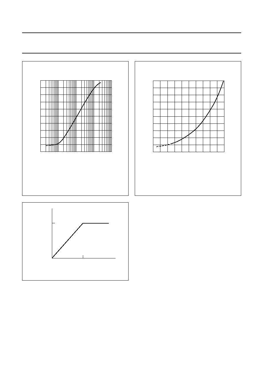
Fig.11 HF envelope output (playback carrier level).
1.3 MHz (NTSC) or 1.4 MHz (PAL) at internal node between head
amplifier and HF AGC.
handbook, halfpage
0
5
1
2
3
4
MGR846
10
-
1
1
10
10
2
10
3
ENVOUT
output
voltage
(V)
left channel carrier amplitude (RMS value) (mV)
Fig.12 AF envelope output (audio peak level).
Bit LOH = 0.
handbook, halfpage
5
0
1
MGR847
2
3
4
-
40
10
-
30
-
20
-
10
0
ENVOUT
output
voltage
(V)
LINEL and LINER output level (dBV)
Fig.13 AGC output of RF converter.
handbook, halfpage
MGR848
RF
converter
output
(dBV)
-
3
-
3
line output (dBV)
6.8
RF converter output
An AGC function is incorporated to avoid overmodulation
in the RF converter connected to pin RFCOUT. The AGC
limits the maximum signal level on the RF converter output
to
-
3 dBV (see Fig.13).
The RF converter output can be muted by setting
bit RFCM = 1. When using this RF converter mute, the
AGC control is reset by discharging the capacitor
connected to pin RFACG.

1999 Apr 14
17
Philips Semiconductors
Product specification
Audio processor with head amplifier for VHS hi-fi
TDA9605H
6.9
Audio dubbing
The TDA9605H includes unparalleled functionality
supporting the audio dubbing function of hi-fi video
recorders. Audio dubbing is a feature which enables the
recording of new sound material on the linear audio track
(i.e. normal sound) of an existing recording. The dub-mix
mode is selected by setting bit IS2 = 1, bit IS1 = 0 and
bit IS0 = 1. Audio dubbing can be used in two different
ways:
∑
Output mix
∑
Input mix.
6.9.1
O
UTPUT MIX
A new additional recording is made on the linear audio
track. In the playback mode, the new linear audio sound
and the original hi-fi sound are combined. In this way the
hi-fi stereo quality remains and the linear audio sound is
partly used (e.g. for commentary only). However, there is
no control over the original hi-fi sound.
Mixing of the hi-fi and normal sound signals in the playback
mode is supported by the output select function mix-left,
mix-right and mix-stereo (bits OSN, OSR and OSL) and
creates a new fixed output signal of
1
/
2
◊
hi-fi plus
1
/
2
◊
normal.
6.9.2
I
NPUT MIX
A new complete recording is made on the linear audio
track (see Fig.4). In the playback mode, only the linear
audio sound is used. In this way the hi-fi stereo quality is
lost, but total freedom in defining the new sound material
is an extra advantage. Furthermore, such recording is no
longer restricted to playback on hi-fi video recorders (with
an output mix option).
The circuit changes into a mixing desk when using the
dub-mix mode of the input select function in combination
with the volume setting of normal select. A new linear
audio recording can be created by mixing together the new
and the original sound.
Continuous user control over amplitude and ratio mix of
the auxiliary input signal (e.g. a microphone input) and the
original hi-fi playback sound is possible using the left and
right channel volume controls. This function is realized
inside the IC by connecting the auxiliary input signal pair
(pins AUXL and AUXR) to the left channel volume control
and the hi-fi output signal pair to the right channel volume
control.
The settings of the output select function are used to
arrange the hi-fi selection and the output signals in the
dub-mix mode. However, some of these settings are
overruled in the dub-mix mode. The normal signal is
available on the line outputs for monitoring the dub-mix
recording signals in the output select function modes
mix-left, mix-right and mix-stereo.
Mix-stereo of the output select function is generally used
for audio dubbing. In combination with the volume setting
of normal select, user control over amplitude and ratio is
offered for the auxiliary and the hi-fi signal as follows:
(
1
/
4
◊
aux left +
1
/
4
◊
aux right)
◊
volume left plus
(
1
/
4
◊
hi-fi left +
1
/
4
◊
hi-fi right)
◊
volume right.
The dub-mix mode is to be used in the (hi-fi) playback
mode. In the record mode, a signal loop from output to
input can be closed which may cause audio oscillation.
The auto-normal switching is not active during the dub-mix
mode. The hi-fi sound is muted when no hi-fi input signal
is detected; bit AUTN is not affected.
Table 5
Dub-mix mode
OUTPUT SELECT
MODE
DUB-MIX OUTPUT
SELECTION
DUB-MIX INPUT
LEFT CHANNEL
RIGHT CHANNEL
mute
mute
aux stereo
mute
hi-fi left
hi-fi left
aux stereo
hi-fi left
hi-fi right
hi-fi right
aux stereo
hi-fi right
hi-fi stereo
hi-fi stereo
aux stereo
hi-fi stereo
normal
normal
aux stereo
mute
mix-left
normal
aux stereo
hi-fi left
mix-right
normal
aux stereo
hi-fi right
mix-stereo
normal
aux stereo
hi-fi stereo
1999 Apr 14
18
Philips Semiconductors
Product specification
Audio processor with head amplifier for VHS hi-fi
TDA9605H
7
I
2
C-BUS PROTOCOL
7.1
Addresses and data bytes
Full control of the TDA9605H is accomplished via the 2-wire I
2
C-bus. Bus speeds up to 400 kbits/s can be used in
accordance with the I
2
C-bus fast-mode specification.
Seven data byte registers are available for programming the device (write mode) and one data byte register is available
for reading data from the device (read mode). The registers are addressable via eight subaddresses. Automatic
subaddress incrementing enables writing of successive data bytes in one transmission.
During power-up, the data byte registers and auto-calibration registers are reset to a default state by the use of a
Power-On Reset (POR) circuit. The reset signal is derived from an internally generated voltage supplied by V
CC
.
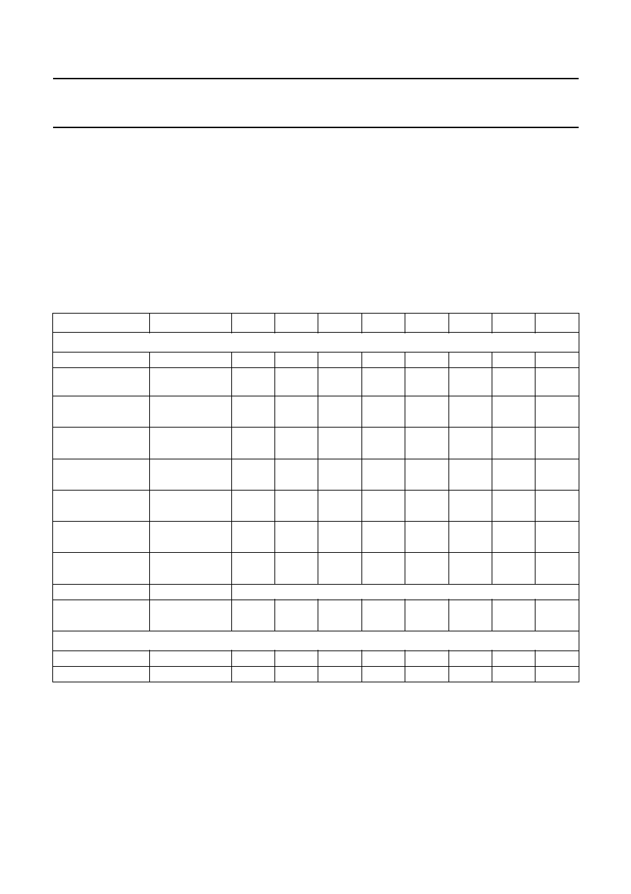
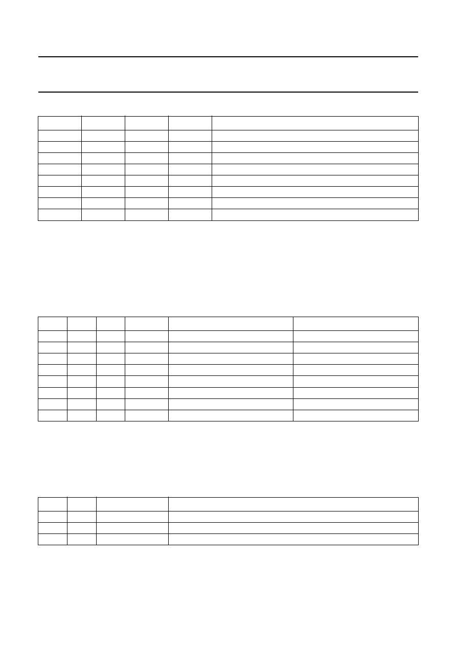
Table 6
Addresses and POR state bits
Notes
1. Continuous writing to a single data byte register is possible when subaddresses F0H to F7H (1111 0xxx) are used
instead of 00H to 07H (0000 0xxx). In that case automatic subaddress incrementing is disabled.
2. It is advised to keep the not-used write bits equal to the POR state to accommodate future compatibility.
3. You cannot rely upon the state of the not-used read bits because their state may change during development.
NAME
ADDRESS
BIT 7
BIT 6
BIT 5
BIT 4
BIT 3
BIT 2
BIT 1
BIT 0
Write mode
Slave byte
B8H
1
0
1
1
1
0
0
0
Subaddress byte
00H to 07H;
note 1
0
0
0
0
0
0 or 1
0 or 1
0 or 1
Control byte
subaddress 00H AFM
DOC
SHH
DETH
NTSC
HAC2
HAC1
HAC0
POR state
1
0
0
0
1
0
0
0
Select byte
subaddress 01H DOS1
DOS0
s5
HRL
NIL3
NIL2
NIL1
NIL0
POR state
0
0
0
(2)
0
0
0
0
0
Input byte
subaddress 02H i7
IS2
IS1
IS0
NS2
NS1
NS0
i0
POR state
0
(2)
0
0
0
1
1
1
0
(2)
Output byte
subaddress 03H LOH
OSN
OSR
OSL
EOS
LOS
DOS
RFCM
POR state
0
0
0
0
0
0
0
1
Left volume byte
subaddress 04H l7
VLS
VL5
VL4
VL3
VL2
VL1
VL0
POR state
0
(2)
1
0
0
0
0
0
0
Right volume byte
subaddress 05H r7
VRS
VR5
VR4
VR3
VR2
VR1
VR0
POR state
0
(2)
1
0
0
0
0
0
0
Volume byte
subaddress 06H simultaneous loading of the subaddress 04H and subaddress 05H registers
Power byte
subaddress 07H CALS
VCCS
TEST
PORR
HPD
MUTE
STBP
STBA
POR state
0
0
0
0
0
1
0
0
Read mode
Slave address byte
B9H
1
0
1
1
1
0
0
1
Read byte
B9H
CALR
AUTN
CALE
POR
0
(3)
0
(3)
0
(3)
0
(3)
1999 Apr 14
19
Philips Semiconductors
Product specification
Audio processor with head amplifier for VHS hi-fi
TDA9605H
7.2
Valid transmissions to and from the TDA9605H
Table 7
Examples of valid transmissions
7.3
Overview of the TDA9605H I
2
C-bus control
Table 8
Condensed overview
FUNCTION
DATA TRANSFER SEQUENCE
Write
START, B8H, 00H, data for 00, STOP
Write with auto-increment
START, B8H, 00H, data for 00, data for 01, data for 02, STOP
Write with auto-increment `wrap-around'
START, B8H, 07H, data for 07, data for 00, data for 01, STOP
Write without auto-increment
START, BBH, F6H, data for 06, data for 06, data for 06, STOP
Read
START, B9H, data from IC, STOP
Read (continued)
START, B9H, data from IC, data from IC, data from IC, STOP
FUNCTION
MODES
CONTROL BITS
Audio FM mode
playback and record
AFM
Playback dropout cancelling
on and off
DOC
Playback head switch noise cancel time
6
µ
s and 8
µ
s
SHH
Playback hi-fi carrier detection time
slow and fast
DETH
Record-mute and carrier ratio select
record-mute, 3, 4.5, 6, 8, 9.5, 11
and 12.5 dB mix ratio
DOC, SHH and DETH
System standard
NTSC and PAL
NTSC
Playback head amplifier amplification
48, 51, 54, 57, 60, 63, 66 and 69 dB
HAC2, HAC1 and HAC0
Record head amplifier current
12.5, 15, 17.5, 21, 25, 30, 35, 42, 50, 60,
71 and 84 mA (p-p)
HAC2, HAC1, HAC0 and HRL
Normal input level
0 to 14 dB and mute
NIL3, NIL2, NIL1 and NIL0
Input select
tuner, CINCH, ext1, ext2, SAP, dub-mix,
normal and aux
IS2, IS1 and IS0
Normal select
input select, volume, input-left,
volume-left, SAP, tuner, ext2 and mute
NS2, NS1 and NS0
Line output amplification
0 dB and +1 dB
LOH
Output select
mute, left, right, stereo, normal, mix-left,
mix-right and mix-stereo
OSN, OSR and OSL
Envelope select
output select, stereo and HF envelope
EOS and AFM
Line select
output select and ext2
LOS
Decoder select
output select, tuner, ext1, SAP and mute DOS, DOS1 and DOS0
RF converter mute
0 dB AGC and mute
RFCM
Volume left
-
47 to 0 dB, mute and 0 to 15 dB
VLS and VL5 to VL0
Volume right
-
47 to 0 dB, mute and 0 to 15 dB
VRS and VR5 to VR0
Auto-calibration
off and start calibration
CALS
Supply voltage select
9 V and 12 V
VCCS
Test
standard operating mode and test mode
TEST, HRL, NIL3, NIL2, NIL1
and NIL0
1999 Apr 14
20
Philips Semiconductors
Product specification
Audio processor with head amplifier for VHS hi-fi
TDA9605H
7.4
Control byte at subaddress 00H
The control byte is used to set the parameters of hi-fi processing and head amplifier control.
7.4.1
A
UDIO
FM
MODE
Bit AFM controls the main mode of the hi-fi processing and head amplifier. The function of other bits of the control byte
and bit EOS of the output byte depends on the state of bit AFM.
Table 9
Audio FM mode selection (bit AFM)
7.4.2
P
LAYBACK MODE
When during the playback mode no FM carrier is detected from tape, the normal audio signal on pin LININ is
automatically selected by the output select function.
For this auto-normal mode:
∑
The timing of the hi-fi carrier detection can be selected via bit DETH which defines the auto-normal release time:
≠ Fast mode: hi-fi detection delay is 1 to 2 HID control signal periods (for NTSC: 33 to 66 ms; for PAL: 40 to 80 ms)
≠ Slow mode: hi-fi detection delay is 7 to 8 HID control signal periods (for NTSC: 233 to 267 ms;
for PAL: 280 to 320 ms).
∑
The state of hi-fi detection and auto-normal can be monitored by I
2
C-bus control bit AUTN of the read byte.
∑
In case automatic selection of the normal audio signal is not required the normal input level control can be set to mute
(bits NIL3 to NIL0 of the select byte).
Table 10 Dropout cancelling (bit DOC), sample-and-hold high-state (bit SHH) and detector time hi-fi (bit DETH) in the
playback mode; note 1
Note
1. X = don't care.
Playback head amplifier disable
standard operating mode and playback
disabled
HPD
Power output muting
power mute
MUTE
Operating mode
standard operating mode, active standby
and passive standby
STBP and STBA
AFM
MODE
DESCRIPTION
0
playback
hi-fi processing in playback mode and head amplifier in playback mode
1
record
hi-fi processing in record mode and head amplifier is in record mode or record-mute mode
AFM DOC SHH DETH
MODE
DESCRIPTION
0
0
X
X
playback and DOC off
dropout cancelling disabled
0
1
X
X
playback and DOC on
dropout cancelling active
0
X
0
X
playback and sample-and-hold time = 6
µ
s
head switch noise cancel time set to 6
µ
s
0
X
1
X
playback and sample-and-hold time = 8
µ
s
head switch noise cancel time set to 8
µ
s
0
X
X
0
playback and hi-fi detect = fast
fast mode hi-fi detector timing
0
X
X
1
playback and hi-fi detect = slow
slow mode hi-fi detector timing
FUNCTION
MODES
CONTROL BITS
1999 Apr 14
21
Philips Semiconductors
Product specification
Audio processor with head amplifier for VHS hi-fi
TDA9605H
7.4.3
R
ECORD MODE
During the record-mute mode, the recording output current on pin RECOUT is muted and the head amplifier is partly
disabled. The record mode, set by I
2
C-bus control, can also be changed to the record-mute mode by an external control
signal on pin RMHID. Sometimes the record-mute mode is named loop-through mode or EE mode.
Table 11 Dropout cancelling (bit DOC), sample-and-hold high-state (bit SHH) and detector time hi-fi (bit DETH) in the
record mode
Note
1. Power-on reset state.
7.4.4
S
YSTEM STANDARD SELECTION
Bit NTSC selects between the NTSC and PAL (SECAM) system carrier frequencies for the CCO modulators or PLL
demodulators and the band-pass filters. FM carrier frequencies of 1.3 and 1.7 MHz are used for the NTSC system where
1.4 and 1.8 MHz are used for the PAL system. Different code settings for the auto-calibration circuit assure proper
calibration using the standard HID control signal frequency of 29.97 Hz for NTSC mode and 25 Hz for PAL mode. After
auto-calibration is completed bit NTSC enables instant switching between the NTSC and PAL system.
Table 12 System standard selection (bit NTSC)
Note
1. Power-on reset state.
AFM
DOC
SHH
DETH
MODE
DESCRIPTION
1
0
0
0
record-mute
record-mute and no recording output current; note 1
1
0
0
1
record and 3 dB mix
recording with 3 dB output carrier ratio (1 : 1.4)
1
0
1
0
record and 4.5 dB mix
recording with 4.5 dB output carrier ratio (1 : 1.7)
1
0
1
1
record and 6 dB mix
recording with 6 dB output carrier ratio (1 : 2)
1
1
0
0
record and 8 dB mix
recording with 8 dB output carrier ratio (1 : 2.5)
1
1
0
1
record and 9.5 dB mix
recording with 9.5 dB standard output carrier ratio (1 : 3)
1
1
1
0
record and 11 dB mix
recording with 11 dB output carrier ratio (1 : 3.5)
1
1
1
1
record and 12.5 dB mix
recording with 12.5 dB output carrier ratio (1 : 4.2)
NTSC
MODE
DESCRIPTION
0
PAL
hi-fi circuit in PAL mode
1
NTSC
hi-fi circuit in NTSC mode; note 1

1999 Apr 14
22
Philips Semiconductors
Product specification
Audio processor with head amplifier for VHS hi-fi
TDA9605H
7.4.5
H
EAD AMPLIFIER PLAYBACK AMPLIFICATION
Eight settings of playback amplification can be selected for the head amplifier. The amplification values are valid for the
head signals from pins PBIN1 or PBIN2 to the internal node between the head amplifier and HF AGC circuit. The setting
of the playback amplification results in a selection of the hi-fi detection level (auto-normal function). The hi-fi detection
level indicated is the RMS value of the left channel carrier signal on pins PBIN1 and PBIN2.
The signal at the internal node can be monitored for testing purposes via pin ENVOUT using test 8 of the test mode.
It should be noted that the output level of test 8 shows 6 dB attenuation compared to the internal node level.
Table 13 Head amplifier control (bits HAC2, HAC1 and HAC0) in the playback mode
7.4.6
H
EAD AMPLIFIER RECORD CURRENT
A total of twelve settings of the recording current can be selected for the head amplifier record output pin RECOUT.
Bit HRL of the select byte selects between high and low current settings. The recording current is defined as the
peak-to-peak value of the current of the record output signal which includes both the left and right carrier signal.
The selected recording current is independent of the selected record mix ratio setting, but recording is disabled during
the record-mute mode as defined by the bits DOC, SHH and DETH or the control signal on pin RMHID.
Table 14 Head amplifier control (bits HAC2, HAC1 and HAC0) and head record current low (bit HRL) in the record
mode
AFM
HAC2
HAC1
HAC0
MODE
DESCRIPTION
0
0
0
0
48 dB
hi-fi detection level equals 13
µ
V (RMS) from head
0
0
0
1
51 dB
hi-fi detection level equals 9.4
µ
V (RMS) from head
0
0
1
0
54 dB
hi-fi detection level equals 6.7
µ
V (RMS) from head
0
0
1
1
57 dB
hi-fi detection level equals 4.7
µ
V (RMS) from head
0
1
0
0
60 dB
hi-fi detection level equals 3.3
µ
V (RMS) from head
0
1
0
1
63 dB
hi-fi detection level equals 2.4
µ
V (RMS) from head
0
1
1
0
66 dB
hi-fi detection level equals 1.7
µ
V (RMS) from head
0
1
1
1
69 dB
hi-fi detection level equals 1.2
µ
V (RMS) from head
AFM
HAC2
HAC1
HAC0
HRL
MODE
DESCRIPTION
1
0
0
0
0
25 mA (p-p)
high recording current is 25 mA (p-p)
1
0
0
1
0
30 mA (p-p)
high recording current is 30 mA (p-p)
1
0
1
0
0
35 mA (p-p)
high recording current is 35 mA (p-p)
1
0
1
1
0
42 mA (p-p)
high recording current is 42 mA (p-p)
1
1
0
0
0
50 mA (p-p)
high recording current is 50 mA (p-p)
1
1
0
1
0
60 mA (p-p)
high recording current is 60 mA (p-p)
1
1
1
0
0
71 mA (p-p)
high recording current is 71 mA (p-p)
1
1
1
1
0
84 mA (p-p)
high recording current is 84 mA (p-p)
1
0
0
0
1
12.5 mA (p-p)
low recording current is 12.5 mA (p-p)
1
0
0
1
1
15 mA (p-p)
low recording current is 15 mA (p-p)
1
0
1
0
1
17.5 mA (p-p)
low recording current is 17.5 mA (p-p)
1
0
1
1
1
21 mA (p-p)
low recording current is 21 mA (p-p)
1999 Apr 14
23
Philips Semiconductors
Product specification
Audio processor with head amplifier for VHS hi-fi
TDA9605H
7.5
Select byte at subaddress 01H
The select byte is used for decoder output select, record current range select and linear audio volume control.
7.5.1
D
ECODER OUTPUT SELECT
By setting bit DOS = 0 of the output byte, the decoder output signal on pins DECL and DECR is defined by the output
select function. However, by setting bit DOS = 1 the decoder select function enables several independent signal
selections controlled via bits DOS1 and DOS0. Via the decoder select function the input signals on pins TUNL
and TUNR, pins EXT1L and EXT1R and pin SAP can be selected. The mute mode can also be selected.
The indicated decoder select function modes are also available during the active standby mode by setting bit STBA = 1.
Table 15 Decoder output select (bits DOS1 and DOS0)
Note
1. Power-on reset state.
7.5.2
H
EAD AMPLIFIER RECORD CURRENT RANGE SELECT
The default selection of eight recording currents set by bits HAC2, HAC1 and HAC0 of the control byte is extended with
four additional low level recording currents by setting bit HRL = 1.
Table 16 Head amplifier record low current (bit HRL)
Note
1. Power-on reset state.
DOS1
DOS0
MODE
DESCRIPTION
0
0
tuner
selection of input signal on pins TUNL and TUNR; note 1
0
1
ext1
selection of input signal on pins EXT1L and EXT1R
1
0
SAP
selection of input signal on pin SAP
1
1
mute
muting the input signal
HRL
MODE
DESCRIPTION
0
high current
selection of 8 medium and high-level recording currents; note 1
1
low current
selection of 4 low-level recording currents
1999 Apr 14
24
Philips Semiconductors
Product specification
Audio processor with head amplifier for VHS hi-fi
TDA9605H
7.5.3
N
ORMAL INPUT LEVEL
Fifteen settings of amplification and mute can be selected for the linear audio input signal on pin LININ. The normal input
level control can replace the manual adjustment of the playback level at the linear audio circuit.
All selections using the normal linear audio signal include the normal input level control.
Table 17 Normal input level (bits NIL3 to NIL0)
Note
1. Power-on reset state.
7.6
Input byte at subaddress 02H
The input byte is used for input selection of the hi-fi and linear audio.
7.6.1
I
NPUT SELECT
The input select function defines the input signal which is forwarded to the volume control function of hi-fi processing and
usually via the normal select function to the external linear audio circuit on pin LINOUT.
Table 18 Input select (bits IS2, IS1 and IS0)
Notes
1. Power-on reset state.
2. The dub-mix mode is a special selection which supports audio dubbing. This video recorder feature enables the
recording of the sound signal of the linear audio only (see Section 6.9).
NIL3
NIL2
NIL1
NIL0
MODE
DESCRIPTION
0
0
0
0
0 dB
amplification of linear audio of 0 dB; note 1
0
0
0
1
1 dB
amplification of linear audio of 1 dB
:
:
:
:
:
:
1
1
0
1
13 dB
amplification of linear audio of 13 dB
1
1
1
0
14 dB
amplification of linear audio of 14 dB
1
1
1
1
mute
linear audio signal muted
IS2
IS1
IS0
MODE
DESCRIPTION
0
0
0
tuner
tuner input signal on pins TUNL and TUNR; note 1
0
0
1
CINCH
CINCH input signal on pins CINL and CINR
0
1
0
ext1
TV input signal on pins EXT1L and EXT1R
0
1
1
ext2
decoder input signal on pins EXT2L and EXT2R
1
0
0
SAP
mono input signal on pin SAP
1
0
1
dub-mix
input signal on pins AUXL and AUXR (for left channel)
and from hi-fi output signal (for right channel); note 2
1
1
0
normal
from linear audio circuit (from pin LININ)
1
1
1
aux
input on pins AUXL and AUXR (e.g. camcorder input)
1999 Apr 14
25
Philips Semiconductors
Product specification
Audio processor with head amplifier for VHS hi-fi
TDA9605H
7.6.2
N
ORMAL SELECT
The normal select function defines which of the input signals is forwarded to pin LINOUT for the connection to an external
linear audio circuit.
Table 19 Normal select (bits NS2, NS1 and NS0)
Note
1. Power-on reset state.
7.7
Output byte at subaddress 03H
The output byte is used for selecting and controlling the output.
7.7.1
L
INE OUTPUT AMPLIFICATION
An additional 1 dB amplification for the line and decoder outputs on pins LINEL, LINER, DECL and DECR can be
selected by the line output high function.
Table 20 Line output high (bit LOH)
Note
1. Power-on reset state.
7.7.2
O
UTPUT SELECT
The auto-normal function is activated when no hi-fi signal is found on tape in the playback mode. Except for the mute
mode, all output select function modes will be overruled and changed to normal. Control of normal input level should be
set to mute for muting the hi-fi sound. The state of the auto-normal function can be monitored by reading bit AUTN of the
read byte.
NS2
NS1
NS0
MODE
DESCRIPTION
0
0
0
input select
left plus right channel signal selected by input select
0
0
1
volume
left plus right channel signal including hi-fi volume control
selected by input select
0
1
0
input-left
left channel only (language 1) selected by input select
0
1
1
volume-left
left channel only (language 1) including hi-fi volume control
selected by input select
1
0
0
SAP
mono input signal from pin SAP
1
0
1
tuner
tuner input signal from pins TUNL and TUNR
1
1
0
ext2
external input signals from pins EXT2L and EXT2R
1
1
1
mute
mute of the input signals; note 1
LOH
MODE
DESCRIPTION
0
0 dB
no line output amplification; note 1
1
1 dB
1 dB line output amplification
1999 Apr 14
26
Philips Semiconductors
Product specification
Audio processor with head amplifier for VHS hi-fi
TDA9605H
Table 21 Output select normal, right and left (bits OSN, OSR and OSL)
Note
1. Power-on reset state.
In case the dub-mix mode is selected via the input select function, the performance of mix-left, mix-right and mix-stereo
modes is changed to support audio dubbing input mixing. The hi-fi channel is available for the input select function and
normal sound is available at the output for monitoring the linear audio recording. The auto-normal state is ignored during
the dub-mix mode and the hi-fi playback signal is muted instead.
Table 22 Dub-mix mode (bits OSN, OSR and OSL)
7.7.3
E
NVELOPE OUTPUT SELECT
The output signal on pin ENVOUT is selected via the envelope select function.
In the playback mode the HF envelope displays the amplitude of the left channel carrier. Display of the right channel
carrier amplitude for special measurement purposes can be selected via test 10 in the test mode.
Table 23 Envelope output select (bit EOS)
Notes
1. X = don't care.
2. Power-on reset state.
OSN
OSR
OSL
MODE
DESCRIPTION
0
0
0
mute
mute; no selection; note 1
0
0
1
left
left hi-fi channel selected (language 1)
0
1
0
right
right hi-fi channel selected (language 2)
0
1
1
stereo
hi-fi stereo selected
1
0
0
normal
normal signal selected (linear audio from pin LININ)
1
0
1
mix-left
mix of hi-fi left with normal (
1
/
2
◊
left +
1
/
2
◊
normal)
1
1
0
mix-right
mix of hi-fi right with normal (
1
/
2
◊
right +
1
/
2
◊
normal)
1
1
1
mix-stereo
mix of hi-fi stereo with normal (
1
/
2
◊
stereo +
1
/
2
◊
normal)
OSN
OSR
OSL
MODE
OUTPUT IN DUB-MIX MODE
INPUT IN DUB-MIX MODE
0
0
0
mute
mute
mute
0
0
1
left
left channel
left channel
0
1
0
right
right channel
right channel
0
1
1
stereo
stereo signal
1
/
2
◊
left +
1
/
2
◊
right
1
0
0
normal
normal signal
mute
1
0
1
mix-left
normal signal
left channel
1
1
0
mix-right
normal signal
right channel
1
1
1
mix-stereo
normal signal
1
/
2
◊
left +
1
/
2
◊
right
AFM
EOS
MODE
DESCRIPTION
X
(1)
0
output select
audio peak envelope of selected signal via output select function; note 2
0
1
HF envelope
HF envelope of the left channel carrier in the playback mode
1
1
stereo envelope
audio peak envelope of the hi-fi stereo signal in the record mode

1999 Apr 14
27
Philips Semiconductors
Product specification
Audio processor with head amplifier for VHS hi-fi
TDA9605H
7.7.4
L
INE OUTPUT SELECT
An independent selection of the input signals from
pins EXT2L and EXT2R to the line outputs on pins LINEL
and LINER is offered by the line select function.
In the active standby mode (bit STBA = 1) the output
select signal is muted. However, the line select function of
the ext2 input signal is still operating.
In combination with the decoder select function a complete
pay-TV decoder switching feature is offered via the
SCART connector.
Table 24 Line output select (bit LOS)
Note
1. Power-on reset state.
7.7.5
D
ECODER OUTPUT SELECT
The output signals on pins DECL and DECR can be
selected by the decoder select function. By setting
bit DOS = 0, the output signals are selected by the output
select function. By setting bit DOS = 1, an independent
selection between the input signals on pins TUNL
and TUNR, pins EXT1L and EXT1R, pin SAP or mute is
possible. These signals are selected by the decoder select
function (bits DOS1 and DOS2).
In the active standby mode (bit STBA = 1) the output
select signal is muted. However, the decoder select
function is still operating.
In combination with the line select function a complete
pay-TV decoder switching feature is offered via the
SCART connector.
Table 25 Decoder output select (bit DOS)
Note
1. Power-on reset state.
LOS
MODE
DESCRIPTION
0
output
select
line output signal is set by output
select; note 1
1
ext2
line output signal is from input
signal on pins EXT2L and EXT2R
DOS
MODE
DESCRIPTION
0
output
select
decoder output signal is set by the
output select function; note 1
1
decoder
select
decoder output signal is set by the
decoder select function
7.7.6
RF
CONVERTER MUTE
The RF converter output signal on pin RFCOUT can be
muted by setting bit RFCM = 1. In this mute mode, the
AGC capacitor on pin RFCAGC is discharged and the
AGC control is reset.
Table 26 RF converter mute (bit RFCM)
Note
1. Power-on reset state.
7.8
Volume bytes at subaddresses 04H, 05H
and 06H
The volume bytes are used to set left and right channel
volume control.
7.8.1
Left and right volume control
Left channel volume control can be set by using
subaddress 04H. Right channel volume control can be set
by using subaddress 05H. Left and right channel volume
control can be set simultaneous by using subaddress 06H.
RFCM
MODE
DESCRIPTION
0
AGC
RF converter output signal is set by
the output select function:
AGC active
1
mute
RF converter output signal is muted
and AGC control is reset; note 1
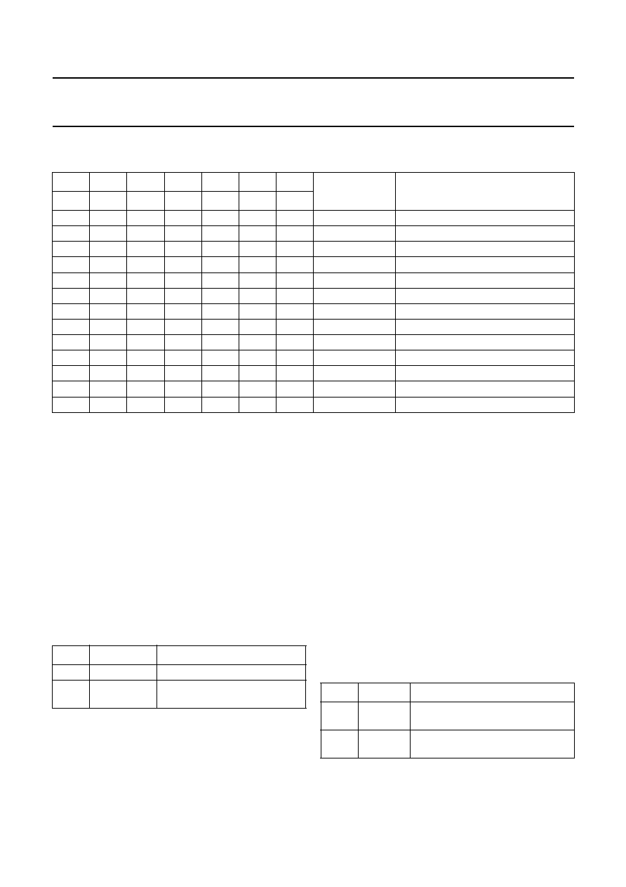
1999 Apr 14
28
Philips Semiconductors
Product specification
Audio processor with head amplifier for VHS hi-fi
TDA9605H
Table 27 Volume left sign (bit VLS), volume left (bits VL5 to VL0), volume right sign (bit VRS) and volume right
(bits VR5 to VR0); note 1
Notes
1. X = don't care.
2. Power-on reset state.
VLS
VL5
VL4
VL3
VL2
VL1
VL0
MODE
DESCRIPTION
VRS
VR5
VR4
VR3
VR2
VR1
VR0
0
0
0
0
0
0
0
0 dB
volume 0 dB
0
0
0
0
0
0
1
-
1 dB
volume
-
1 dB
0
0
0
0
0
1
0
-
2 dB
volume
-
2 dB
:
:
:
:
:
:
:
:
:
0
1
0
1
1
1
0
-
46 dB
volume
-
46 dB
0
1
0
1
1
1
1
-
47 dB
volume
-
47 dB
0
1
1
X
X
X
X
mute
mute
1
X
X
0
0
0
0
0 dB
volume 0 dB; note 2
1
X
X
0
0
0
1
1 dB
volume 1 dB
1
X
X
0
0
1
0
2 dB
volume 2 dB
:
:
:
:
:
:
:
:
:
1
X
X
1
1
1
0
14 dB
volume 14 dB
1
X
X
1
1
1
1
15 dB
volume 15 dB
7.9
Power byte at subaddress 07H
The power byte is used for power-up settings and the
standby control mode.
7.9.1
C
ALIBRATION START
Automatic frequency calibration by setting the hi-fi modem,
the band-pass filter and the noise reduction is performed
after a change of bit CALS from logic 0 to logic 1. The use
of auto-calibration is only needed after power-up
(Power-on reset) of the supply voltage (see Section 6.5).
Table 28 Calibration start (bit CALS)
Note
1. Power-on reset state.
The output signal on pin ENVOUT or bit CALR (calibration
ready) and bit CALE (calibration error) of the read byte can
be monitored to check for completion of the calibration.
CALS
MODE
DESCRIPTION
0
no calibration note 1
1
start
calibration
start of the automatic calibration
cycle
The combination of bit CALR = 1 and bit CALE = 0
indicates a successful calibration. Bit CALS should remain
at logic 1 after the calibration to keep a reliable state of
bit CALR and bit CALE.
7.9.2
DC
OUTPUT VOLTAGE SELECTION
The DC output level on pins LINEL, LINER, DECL
and DECR can be changed by setting bit VCCS to
maximize the output power when using a supply voltage
of 12 V.
The use of power muting (bit MUTE = 1) ensures
disturbance free switching of the line output signal when
setting bit VCCS after power-up.
Table 29 V
CC
supply voltage select (bit VCCS)
Note
1. Power-on reset state.
VCCS
MODE
DESCRIPTION
0
9 V
line and decoder output DC voltage
is 4.5 V; note 1
1
12 V
line and decoder output DC voltage
is 6 V
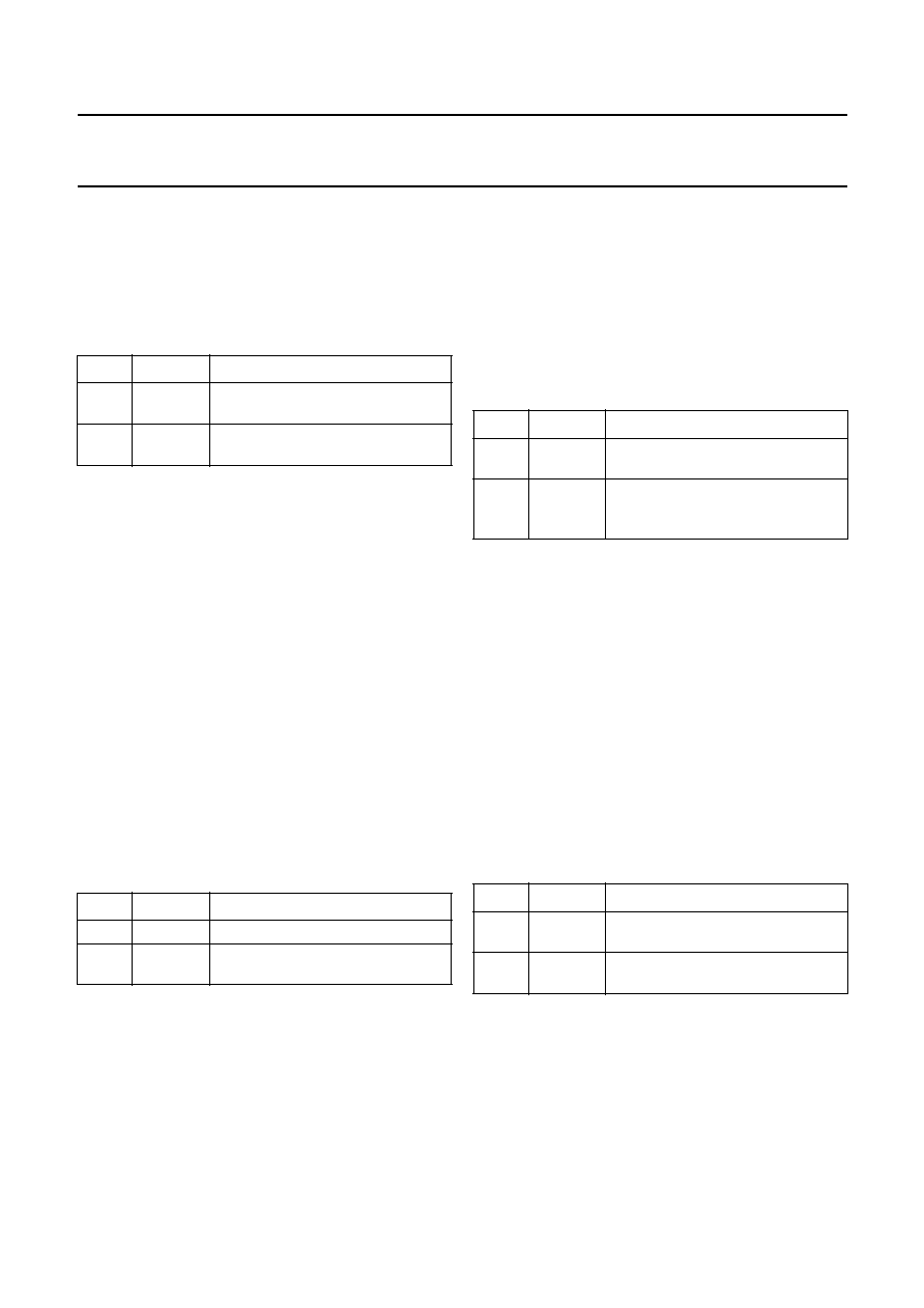
1999 Apr 14
29
Philips Semiconductors
Product specification
Audio processor with head amplifier for VHS hi-fi
TDA9605H
7.9.3
T
EST MODE
Several special tests can be selected for test, evaluation
and measurement purposes. The selection of these tests
is made by setting bit HRL and bits NIL3 to NIL0.
See Section 14.4 for an overview of the test modes.
Table 30 Test mode (bit TEST)
Note
1. Power-on reset state.
7.9.4
P
OWER
-
ON RESET
Setting bit PORR = 1 ensures a reset of bit POR of the
read byte to logic 0. In this way, a reading of logic 1 for
bit POR always indicates the occurrence of an actual
I
2
C-bus register Power-on reset and can not be caused
accidentally by other I
2
C-bus control bits. Bit PORR has no
control function but it is an unused bit, dedicated by name
to change the I
2
C-bus register content from the Power-on
reset state.
Bit POR of the read byte is a logic AND function for
checking all I
2
C-bus register bits. Bit POR will read logic 1
when the I
2
C-bus register content equals the Power-on
reset default state and also when this state is set via the
I
2
C-bus control. Since a setting of bit PORR = 1 differs
from the Power-on reset default state, it forces a reset of
bit POR to logic 0 independent of other bit settings.
Table 31 Resetting of bit POR (bit PORR)
Note
1. Power-on reset state.
TEST
MODE
DESCRIPTION
0
operating
mode
standard operating; note 1
1
test mode test mode for special
measurements
PORR
MODE
DESCRIPTION
0
no reset
note 1
1
bit POR
reset
reset of bit POR (read byte)
7.9.5
H
EAD AMPLIFIER DISABLE
Bit HPD offers a special setting intended for use with some
of the built-in test modes and for support of particular
applications that do not require use of the integrated head
amplifier. By setting bit HPD = 1 the head amplifier
playback circuit is disabled. This mode enables direct input
signal to the HF AGC circuit via pin HMSW (AC coupled
via a 10 nF capacitor).
Table 32 Head amplifier playback disable (bit HPD)
Note
1. Power-on reset state.
7.9.6
P
OWER MUTING
The power mute function controls the mute switches on the
line and RF converter outputs. The power mute mode is
automatically activated via the Power-on reset function
during power-up of the supply voltage. During
power-down, the mute switches are activated
automatically by means of the auto-mute circuit which is
independent of the setting of bit MUTE. When setting
bit MUTE = 1 the output current on pins RFCOUT, LINEL,
LINER, DECL and DECR is limited to
-
1 mA for controlled
power-up response and the selected output signal is
muted (see Section 6.6).
Table 33 Power mute (bit MUTE)
Note
1. Power-on reset state.
HPD
MODE
DESCRIPTION
0
operating
mode
standard operating mode; note 1
1
head
amplifier
disable
head amplifier disabled in playback
mode (for test or special
application)
MUTE
MODE
DESCRIPTION
0
no mute
power muting released: mute
switches are open
1
mute
power muting activated: mute
switches are closed; note 1
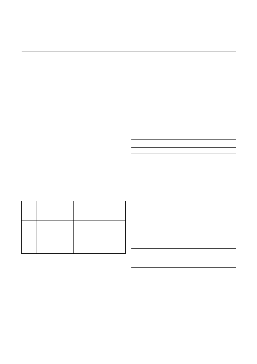
1999 Apr 14
30
Philips Semiconductors
Product specification
Audio processor with head amplifier for VHS hi-fi
TDA9605H
7.9.7
S
TANDBY SELECT
The TDA9605H is switched in the low-power active
standby mode by setting bit STBA = 1. Most circuits are
switched inactive for reducing power consumption.
However, the RF converter, line and decoder outputs
remain active in this mode and the direct audio selections
offered via the line select function and the decoder select
function remain available. The selected output signal is
muted during the active standby mode.
The TDA9605H is switched in the minimum power passive
standby mode by setting bit STBP = 1. All circuits are
switched inactive to obtain minimum power consumption
except for the power mute circuit, the I
2
C-bus and the line
input reference buffer (i.e. the DC voltage on pins 1 to 11
remains active). When bit STBP = 1 a discharge current of
1 mA is active on pins RFCOUT, LINEL, LINER, DECL
and DECR.
Power muting ensures disturbance-free switching of the
line and RF converter outputs to and from the passive
standby mode. In the passive standby mode power muting
can be de-activated again to achieve minimum power
consumption. The calibration and I
2
C-bus registers are not
affected in the active standby or passive standby mode.
Table 34 Standby passive (bit STBP) and standby active
(bit STBA); note 1
Notes
1. X = don't care.
2. Power-on reset state.
7.10
Read byte
The read byte is used for reading the device state
information.
STBP
STBA
MODE
DESCRIPTION
0
0
operating
standard operating mode:
full function; note 2
0
1
active
standby
active standby mode:
reduced power
consumption
1
X
passive
standby
passive standby mode:
minimum power
consumption
7.10.1
C
ALIBRATION READY
The completion of calibration is signalled by changing
bit CALR from logic 0 to logic 1. Bit CALR remains logic 0
if for some reason a calibration can not be completed (i.e.
no HID control signal available or the hi-fi processing is in
the playback mode). Bit CALR will also return to logic 0 if
calibration is lost due to a Power-on reset situation.
Additional information about the calibration result is
available via bit CALE. Calibration is found correct if
bit CALR = 1 and bit CALE = 0.
Pin ENVOUT can also be used to monitor calibration
(see Section 6.5).
Table 35 Calibration ready (bit CALR)
Note
1. Power-on reset state.
7.10.2
A
UTO
-
NORMAL SELECTION
The auto-normal function is activated when no hi-fi carrier
input signal is detected in the playback mode.
The auto-normal function overrules the settings of the
output select function and selects normal sound (i.e. linear
audio) instead of hi-fi. The state of the auto-normal
function can be checked by reading bit AUTN.
The auto-normal function and therefore bit AUTN is only
valid in the playback mode. Bit AUTN is always logic 0 in
the record mode.
Table 36 Auto-normal (bit AUTN)
Note
1. Power-on reset state.
CALR
DESCRIPTION
0
not calibrated; note 1
1
auto-calibration completed
AUTN
DESCRIPTION
0
hi-fi carrier available; audio FM signal is
detected from tape in playback mode; note 1
1
normal sound selected instead of hi-fi carrier;
no audio FM signal is detected from tape

1999 Apr 14
31
Philips Semiconductors
Product specification
Audio processor with head amplifier for VHS hi-fi
TDA9605H
7.10.3
C
ALIBRATION ERROR
An unreliable calibration result is indicated when reading
bit CALE = 1. The calibration result is not reliable when
during calibration the control signal on pin RMHID is
disturbed due to an external cause. Such a disturbance of
the HID control signal is detected when reading
bit CALE = 1. A new calibration should be started to
ensure proper calibration.
Calibration is found correct when bit CALR = 1 and
bit CALE = 0.
Table 37 Calibration error (bit CALE)
Note
1. Power-on reset state.
7.10.4
P
OWER
-
ON RESET
An internal Power-on reset signal is generated at
power-up or during a power voltage dip. The I
2
C-bus data
bits and auto-calibration registers are reset to a
pre-defined state. When reading bit POR = 1, it indicates
that the internal data bits are found to be in the POR state
due to an actual Power-on reset or the I
2
C-bus control
settings.
CALE
DESCRIPTION
0
not calibrated or calibration result is found
correct; note 1
1
calibration error encountered during calibration
Detecting the occurrence of a Power-on reset by reading
bit POR requires a setting of bit PORR = 1 after power-up.
Bit POR is forced to logic 0 only by setting bit PORR = 1,
so this setting is independent of other I
2
C-bus bit settings.
After calibration a Power-on reset occurrence is also
indicated by bit CALR = 0, because calibration will be lost.
Table 38 Power-on reset (bit POR)
Note
1. Power-on reset state.
POR
DESCRIPTION
0
I
2
C-bus bit state differs from the Power-on reset
state
1
I
2
C-bus bit state equals the Power-on reset
state; note 1
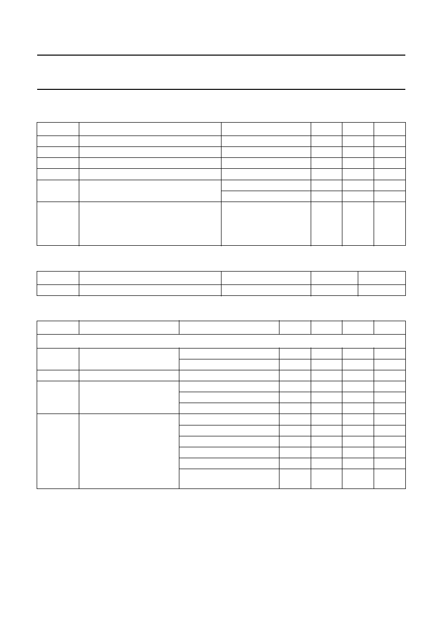
1999 Apr 14
32
Philips Semiconductors
Product specification
Audio processor with head amplifier for VHS hi-fi
TDA9605H
8
LIMITING VALUES
In accordance with the Absolute Maximum Rating System (IEC 134).
9
THERMAL CHARACTERISTICS
10 GENERAL CHARACTERISTICS
SYMBOL
PARAMETER
CONDITIONS
MIN.
MAX.
UNIT
V
CC
supply voltage
0
13.2
V
V
CCH
head amplifier supply voltage
0
5.5
V
T
stg
storage temperature
-
65
+150
∞
C
T
amb
operating ambient temperature
0
70
∞
C
V
es
electrostatic handling voltage
machine model
-
300
+300
V
human body model
-
3000
+3000
V
I
lu(prot)
latch-up protection current on
T
j
= 100
∞
C
pin HSMW
-
70
+100
mA
pin SDA
-
60
+100
mA
all other pins
-
100
+100
mA
SYMBOL
PARAMETER
CONDITIONS
VALUE
UNIT
R
th(j-a)
thermal resistance from junction to ambient
in free air
60
K/W
SYMBOL
PARAMETER
CONDITIONS
MIN.
TYP.
MAX.
UNIT
Supplies
V
CC
supply voltage
VCCS = 0
8.1
9
13.2
V
VCCS = 1
8.1
12
13.2
V
V
CCH
head amplifier supply voltage
4.75
5
5.5
V
I
CC
supply current
standard operating mode
-
36
48
mA
active standby (STBA = 1)
-
8
12
mA
passive standby (STBP = 1)
-
4
6
mA
I
CCH
head amplifier supply current
playback mode
-
21
28
mA
record-mute mode
-
18
24
mA
record mode (HAC = 000)
-
23
31
mA
record mode (HAC = 011)
-
35
47
mA
record mode, (HAC = 111)
-
67
89
mA
active or passive standby
(STBA = 1 or STBP = 1)
-
0
-
mA

1999 Apr 14
33
Philips Semiconductors
Product specification
Audio processor with head amplifier for VHS hi-fi
TDA9605H
11 RECORD-MUTE MODE CHARACTERISTICS
V
CC
= 12 V; T
amb
= 25
∞
C; tuner audio input level
-
8 dBV at f = 1 kHz; Power-on reset state with output select = stereo;
bit RFCM = 0; bit MUTE = 0; auto-calibrated; measured in typical application circuit of Fig.14; unless otherwise
specified.
Internally generated voltage levels
V
n1
DC voltage on pins SAP,
TUNL, TUNR, CINL, CINR,
EXTL1, EXTLR, AUXL,
AUXR, LININ and RFCOUT
-
3.8
-
V
V
n2
DC voltage on pin LINOUT
-
4.5
-
V
V
n3
DC voltage on pins LINEL,
LINER, DECL and DECR
V
CC
= 9 V (VCCS = 0)
-
4.5
-
V
V
CC
=12 V (VCCS = 1)
-
6
-
V
Control signal input: pin RMHID
V
I
input voltage
record or record-mute with
I
2
C-bus control (RM = LOW)
for head 2 (HID = LOW)
0
-
0.6
V
for head 1 (HID = HIGH)
1.0
-
2.35
V
record-mute (RM = HIGH)
for head 2 (HID = LOW)
2.65
-
3.8
V
for head 1 (HID = HIGH)
4.3
-
5.5
V
SYMBOL
PARAMETER
CONDITIONS
MIN.
TYP.
MAX.
UNIT
Line inputs: pins SAP, TUNL, TUNR, CINL, CINR, EXT1L, EXT1R, EXT2L, EXT2R, AUXL and AUXR
V
i
input voltage
-
-
9
dBV
R
i
input impedance
100
130
-
k
Linear audio input: pin LININ
V
i
input voltage
-
-
8
dBV
R
i
input impedance
100
130
-
k
Linear audio output: pin LINOUT
V
o
output voltage
-
9
-
8
-
7
dBV
R
o
output impedance
-
200
300
Line and decoder outputs: pins LINEL, LINER, DECL and DECR
V
o
output voltage
normal output (LOH = 0)
-
9
-
8
-
7
dBV
output = 1 dB (LOH = 1)
-
8
-
7
-
6
dBV
V
o(max)
maximum output voltage
V
CC
= 9 V; note 1
7
8
-
dBV
V
CC
= 12 V; note 1
10
11
-
dBV
I
o(dch)
discharge output current
passive standby (STBP = 1)
-
1
-
mA
I
o(max)
output current limiting
power mute (MUTE = 1)
-
-
1
-
mA
R
o
output impedance
-
100
150
THD
total harmonic distortion
-
0.01
0.1
%
SYMBOL
PARAMETER
CONDITIONS
MIN.
TYP.
MAX.
UNIT
1999 Apr 14
34
Philips Semiconductors
Product specification
Audio processor with head amplifier for VHS hi-fi
TDA9605H
Notes
1. THD = 1%, output load with R
L
= 5 k
and C
L
= 2.2 nF, volume = 3 dB for V
CC
= 12 V and tuner input level varied.
2. B = 20 Hz to 20 kHz, unweighted.
3. Crosstalk of any line input pair (tuner, CINCH, ext1, ext2, aux and SAP) to any other line input.
cb
channel balance
-
1
0
+1
dB
V
n
noise level
tuner input signal at zero level
-
dBV; note 2
-
-
94
-
90
dBV
mute(v)
mute volume
volume bytes left and right set
to mute mode
-
-
96
-
70
dB
mute(o)
mute output
output select bits set to mute
mode
-
-
86
-
70
dB
ct(ch)
crosstalk between channels
one of tuner input signals at
zero level
-
dBV
-
-
90
-
70
dB
ct(ch)(i)
crosstalk between input
channels
note 3
-
<
-
93
-
dB
RF converter output: pin RFCOUT
V
o
output voltage
tuner input signal at
normal level -8 dB
-
9
-
8
-
7
dBV
high level 8 dBV
-
4.5
-
3
-
1.5
dBV
THD
total harmonic distortion
tuner input signal at
normal level
-
8 dBV
-
0.03
-
%
levels from
-
8 to +8 dBV
-
<0.2
-
%
V
n
noise level
tuner input signal on zero level
-
dBV; note 2
-
-
80
-
dBV
R
o
output impedance
-
200
300
I
o(max)
output current limiting
power mute (MUTE = 1)
-
-
1
-
mA
I
o
discharge output current
passive standby (STBP = 1)
-
1
-
mA
Power mute outputs: pins MUTEC, MUTEL and MUTER
R
o
output impedance
no mute (MUTE = 0)
50
100
-
k
muting (MUTE = 1);
DC load from
-
1 to +1 mA
-
15
-
Audio peak envelope output: pin ENVOUT
V
o
output voltage
tuner input signal at
normal level
-
8 dBV
1.65
1.8
1.96
V
at high level +8 dBV
4.0
4.5
5.0
V
at zero level
-
dBV
-
-
0.3
V
at zero level
-
dBV and
maximum volume +15 dB
-
-
0.35
V
cb
channel balance
-
0.11
0
+0.11
V
R
o
output impedance
-
1
1.5
k
SYMBOL
PARAMETER
CONDITIONS
MIN.
TYP.
MAX.
UNIT
1999 Apr 14
35
Philips Semiconductors
Product specification
Audio processor with head amplifier for VHS hi-fi
TDA9605H
12 RECORD MODE CHARACTERISTICS
V
CC
= 12 V; T
amb
= 25
∞
C; tuner audio input level
-
8 dBV at f = 1 kHz; auto-calibrated; measured in typical application
circuit of Fig.14; unless otherwise specified.
Notes
1. B = 20 Hz to 20 kHz, unweighted.
2. Amplitude of 400 kHz intermodulation product f
c(R)
and f
c(L)
compared to amplitude of recording current f
c(R)
+ f
c(L)
.
SYMBOL
PARAMETER
CONDITIONS
MIN.
TYP.
MAX.
UNIT
Noise reduction (test 25b)
THD
total harmonic distortion
tuner input signal at
normal level
-
8 dBV
-
0.1
0.3
%
high level +8 dBV
-
0.2
1.0
%
cb
channel balance
-
1
0
+1
dB
lin
linearity
tuner input signal at
low level
-
68 to
-
8 dBV
-
32
-
30.5
-
29
dB
high level
-
8 to +8 dBV
7.5
8
8.5
dB
n
noise level with respect to
signal level
tuner input signal level
from
-
to
-
8 dBV; note 1
-
-
46
-
41
dB
t
att
attack time
in accordance with VHS specification
-
5
-
ms
t
rec
recovery time
in accordance with VHS specification
-
70
-
ms
res(f1)
frequency response 300 Hz
tuner input frequency from
300 to 1000 Hz
-
0.7
-
0.2
+0.3
dB
res(f2)
frequency response 10 kHz
tuner input frequency from
10 to 1 kHz
3.1
3.9
4.7
dB
res(lpf1)
audio low-pass filter
response 20 kHz
tuner input frequency from
20 to 1 kHz; test 26b
-
0.5
-
0.1
+0.5
dB
res(lpf2)
audio low-pass filter
response 60 kHz
tuner input frequency from
60 to 1 kHz; test 26b
-
-
24
-
12
dB
FM modulator
THD
total harmonic distortion
f
FM
= 50 kHz; test 25a and 26a
-
0.1
0.2
%
f
FM(max)
maximum FM deviation of
clipper
test 25a and 26a
140
150
160
kHz
f
c(acc)
carrier frequency accuracy
auto-calibration
-
5
0
+5
kHz
f
c
carrier frequency difference
f
c(R)
-
f
c(L)
for NTSC auto-calibration
399.2
401.2
403.2
kHz
f
c(shift)
carrier frequency shift
NTSC/PAL system switching
97
100
103
kHz
TC
temperature coefficient
-
±
50
-
ppm/K
Noise reduction and FM modulator
f
FM
FM deviation
44.5
50
56.1
kHz
Record output on pin RECOUT
I
o(acc)
output current accuracy
left and right carrier 1st harmonic
-
1.5
0
+1.5
dB
f(acc)
carrier mix ratio accuracy
left compared to right carrier
-
1
0
+1
dB
IM2
IM2 product
note 2
-
-
66
-
dB
1999 Apr 14
36
Philips Semiconductors
Product specification
Audio processor with head amplifier for VHS hi-fi
TDA9605H
13 PLAYBACK MODE CHARACTERISTICS
V
CC
= 12 V; T
amb
= 25
∞
C; measured in typical application circuit of Fig.14; unless otherwise specified.
SYMBOL
PARAMETER
CONDITIONS
MIN.
TYP.
MAX.
UNIT
Play back input on pins PBIN2 and PBIN1
R
i
input resistance
-
700
-
C
i
input capacitance
-
35
-
pF
V
n(i)
input noise voltage
-
0.5
-
nV/
Hz
I
n(i)
input noise current
-
2.5
-
pA/
Hz
Head mode switch: pin HSMW
R
i
input impedance
with respect to ground
-
1
2
Head amplifier
G
acc
gain accuracy
test 8
-
3
0
+3
dB
G
bal
gain balance
between pins PBIN1 and PBIN2
-
1
0
+1
dB
ct
head-to-head crosstalk
between pins PBIN1and PBIN2
-
-
45
-
dB
HF AGC (test 5)
V
i(p-p)
AGC start level
(peak-to-peak value)
playback mode (HPD = 1);
left plus right channel
47
67
94
mV
B
control bandwidth
note 1
-
10
-
kHz
Left channel band-pass filter (test 3)
f
output voltage ratio
(f
0
-
400 kHz)/f
0
-
-
30
-
20
dB
(f
0
-
150 kHz)/f
0
-
9
-
6
-
dB
(f
0
+ 150 kHz)/f
0
-
9
-
5
-
dB
(f
0
+ 250 kHz)/f
0
-
-
17
-
12
dB
(f
0
+ 250 kHz)/(f
0
+ 150 kHz)
-
-
12
-
9
dB
(f
0
+ 400 kHz)/f
0
-
-
-
30
dB
t
d(g)
ripple group delay
(f
0
-
150 kHz) to (f
0
+ 150 kHz)
-
0.5
-
µ
s
Right channel band-pass filter (test 4)
f
output voltage ratio
(f
0
-
400 kHz)/f
0
-
-
-
30
dB
(f
0
-
250 kHz)/f
0
-
-
17
-
10
dB
(f
0
-
250 kHz)/(f
0
-
150 kHz)
-
-
12
-
9
dB
(f
0
1 150 kHz)/f
0
-
9
-
5
-
dB
(f
0
+ 150 kHz)/f
0
-
9
-
6
-
dB
(f
0
+ 400 kHz)/f
0
-
-
30
-
20
dB
t
d(g)
ripple group delay
(f
0
-
150 kHz) to (f
0
+ 150 kHz)
-
0.5
-
µ
s
1999 Apr 14
37
Philips Semiconductors
Product specification
Audio processor with head amplifier for VHS hi-fi
TDA9605H
Hi-fi detector (bit AUTN)
V
th(rms)
threshold level (RMS value)
playback mode (HPD = 1);
left channel carrier
2.4
3.3
4.6
mV
V
th(acc)
accuracy of threshold level
left channel carrier on pins PBIN1
and PBIN2
-
5
0
+5
dB
t
d(sw)
switch-on delay
carrier to no-carrier
150
300
500
µ
s
Hi-fi dropout cancelling (bit DOC)
V
th
threshold level
with respect to threshold level of
bit AUTN
-
7
-
4
-
2
dB
t
d(sw)
switch-off delay
no-carrier to carrier
5
9
14
µ
s
Head switching noise suppression
t
h
hold time
sample-and-hold time bit SHH = 0 5
6
7
µ
s
sample-and-hold time bit SHH = 1 7
8
9
µ
s
THD
total harmonic distortion
test 25c; note 2
-
-
-
73
dB
t
d
delay
between HID control signal and
hold status
-
0.3
-
µ
s
PLL FM demodulator (test 25c)
V
i
sensitivity
f
FM
= 150 kHz; S/N = 35 dB
-
0.3
1
mV
THD
total harmonic distortion
normal;
f
FM
= 50 kHz
-
0.05
0.3
%
maximum;
f
FM
= 150 kHz
-
0.2
1.5
%
S/N
signal-to-noise ratio
f
FM
= 50 to 0 kHz
54
60
-
dB
ct(ch)
channel crosstalk
left or right carrier;
f
FM
= 0 kHz
-
-
80
-
dB
Noise reduction (test 26c)
V
n
noise level
tuner input signal level
at
-
dBV; note 3
-
-
95
-
90
dBV
THD
total harmonic distortion
tuner input signal level
at
-
6.5 dBV
-
0.05
0.2
%
lin
linearity
tuner input signal level
from
-
6.5 to
-
36.5 dBV
58
59.6
62
dB
res(f1)
frequency response 300 Hz
tuner input frequency from
300 to 1000 Hz
-
0.6
+0.4
+1.4
dB
res(f2)
frequency response 10 kHz
tuner input frequency from
10 to 1 kHz
-
9.2
-
7.7
-
6.2
dB
SYMBOL
PARAMETER
CONDITIONS
MIN.
TYP.
MAX.
UNIT
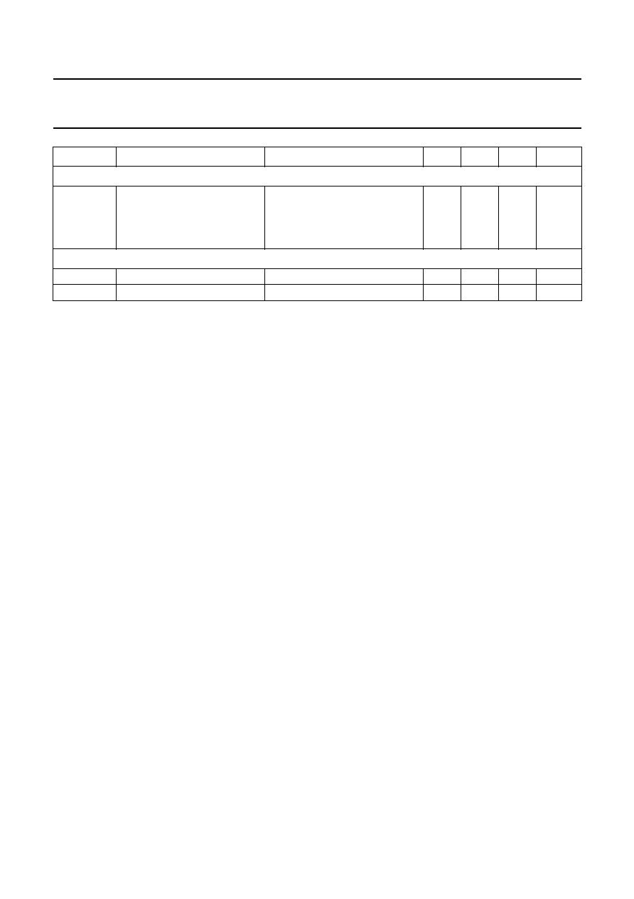
1999 Apr 14
38
Philips Semiconductors
Product specification
Audio processor with head amplifier for VHS hi-fi
TDA9605H
Notes
1. Amplitude modulated single carrier signal of 60 mV (RMS) on pin HMSW; for playback mode HPD = 1. Control
bandwidth is defined as the modulation frequency at which the amplitude modulation is attenuated with 3 dB by the
HF AGC.
2. Sample-and-hold audio distortion is measured using a HID control signal of 500 Hz on pin RMHID, f
mod
= 10 kHz and
f
FM
= 50 kHz. Audio distortion is measured using a 3 kHz 4th-order low-pass filter. The measured value is corrected
with 24 dB in order to calculate the equivalent distortion for the standard NTSC 29.97 Hz HID control signal.
3. B = 20 Hz to 20 kHz, unweighted.
Envelope output: pin ENVOUT
V
o
output voltage
left channel input signal at
1.6 mV (RMS)
0.6
0.9
1.2
V
16 mV (RMS)
2.5
2.9
3.3
V
160 mV (RMS)
4.2
4.7
5.0
V
FM demodulator and noise reduction: pins LINEL and LINER
V
o
output voltage
-
10
-
8
-
6
dBV
cb
channel balance
-
1.5
0
+1.5
dB
SYMBOL
PARAMETER
CONDITIONS
MIN.
TYP.
MAX.
UNIT

1999
Apr
14
39
Philips Semiconductors
Product specification
Audio processor with head amplifier for VHS hi-fi
TDA9605H
This text is here in white to force landscape pages to be rotated correctly when browsing through the pdf in the Acrobat reader.This text is here in
_
white to force landscape pages to be rotated correctly when browsing through the pdf in the Acrobat reader.This text is here inThis text is here in
white to force landscape pages to be rotated correctly when browsing through the pdf in the Acrobat reader. white to force landscape pages to be ...
14
APPLICA
TION AND TEST INFORMA
TION
n
dbook, full pagewidth
MGR839
M
M
M
M
TUL
head drum
AH1
AH2
5 V
1
2
3
4
40
39
37
35
36
38
5
6
7
SAP
TUL
TUR
E1L
E1R
E2L
E2R
8
9
10
N
dub
11
normal select
input select
volume right
M
normal
input
level
RF converter
mute
volume left
decoder
select
+
1 dB 12 V
TDA9605H
1.7 or 1.8 MHz
SAP
21
22
TUR
DCL
DCR
HID
HID
SDA
SCL
26
25
24
23
TUL
E1L
SAP
TUR
E1R
E2L
E2R
VCC
SAP
+
+
+
+
+
+
41
44
42
43
standby select
SUPPLY
34
27
29
28
M
+
E2L
E2R
+
HF LFP
L
DCR
R
N
dub
HF LIMITER
PEAK HOLD
LEVEL
DETECTOR
PLL
CCO
(1.7 or
1.8 MHz)
LEVEL
DETECTOR
DROPOUT
CANCELING
HI-FI
DETECTOR
1.3 or 1.4 MHz
HF LFP
HF AGC
M
HF LIMITER
PLL
CCO
(1.3 or
1.4 MHz)
envelope output
select
+
record
envelope
output
select
+
playback
DCL
mute
R
L
PEAK HOLD
AUTO-MUTE
line select
output select
AUTN
AUTN
M
NOISE
SUPPRESSION
NOISE
SUPPRESSION
RECTIFIER
NOISE REDUCTION
FM (DE-)MODULATOR
HEAD AMPLIFIER
I/O CONTROL
CCA
W
+
FM
5th ORDER
AUDIO LPF
COMPRESSOR
EXPANDER
DETECTOR
AUDIO
CLIPPER
I
2
C-BUS
INTERFACE
M = mute
I
2
C-bus
control
HID
RM
RM
HID
AF/HF envelope
RM
19
20
16
15
17
18
13
14
AUDIO
CLIPPER
12
30
31
32
33
RECTIFIER
CCA
W
+
FM
5th ORDER
AUDIO LPF
COMPRESSOR
EXPANDER
DETECTOR
10 k
18 k
470
47
µ
F
10 nF
100 nF
100 nF
2.7 k
33 k
10
µ
F
10
µ
F
47
µ
F
6.8 nF
2.7 k
33 k
10
µ
F
10
µ
F
47
µ
F
6.8 nF
10
µ
F
decoder
line
10
µ
F
RFC
10
µ
F
10
µ
F
10
µ
F
3.3 M
10
µ
F
220 nF
10
µ
F
linear audio
SAP
tuner
CINCH
ext1
ext2
aux
220 nF
(11
◊
)
39 k
(2%)
47
µ
F
2.2
µ
F
10 nF
9 to 12 V
playback.
+
record-mute,
recording
carrier ratio select,
record-mute
playback head
amplification,
record head
current
Fig.14 Application diagram.

1999 Apr 14
40
Philips Semiconductors
Product specification
Audio processor with head amplifier for VHS hi-fi
TDA9605H
14.1
RM and HID control signals
To assure proper input conditions on pin RMHID the RM and HID control signals (see Fig.15) should satisfy the
requirements given in Table 39.
Table 39 Conditions of RM and HID input signal
14.2
Reference current resistor
The requirements for the reference current resistor on pin 28 are:
∑
R = 39 k
±
2%
∑
Temperature coefficient =
±
50 ppm/
∞
C.
SIGNAL
HID INPUT SIGNAL ONLY
HID AND RM INPUT SIGNALS
CONDITIONS
MIN.
MAX.
CONDITIONS
MIN.
MAX.
HID
LOW
0 V
1.5 V
LOW
0 V
0.4 V
HIGH
3 V
5.5 V
HIGH
4.3 V
5.5 V
RM
grounded
-
-
LOW
0 V
0.4 V
HIGH
4.3 V
5.5 V
Fig.15 RMHID input.
a. HID input only.
b. HID and RM input.
handbook, full pagewidth
MGR840
10 k
(5 %)
18 k
(5 %)
TDA9605H
RMHID
HID
41
10 k
(5 %)
18 k
(5 %)
TDA9605H
RMHID
HID
RM
RM
41
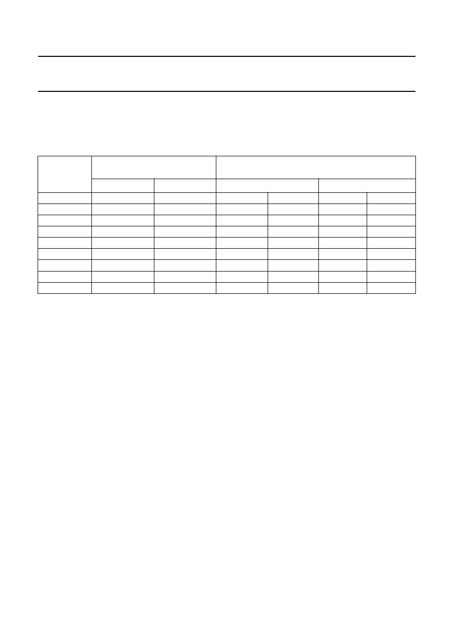
1999 Apr 14
41
Philips Semiconductors
Product specification
Audio processor with head amplifier for VHS hi-fi
TDA9605H
14.3
Setting line output level
The audio level can be set by selecting the external filter components connected to the emphasis noise reduction
pins 24 and 32 (pins EMPHL and EMPHR).
Table 40 Component values for setting the line output level
Note
1. Standard 50 kHz FM deviation at f = 1 kHz.
14.4
Test modes
Special test modes are implemented for testing, evaluation and measurement purposes. These test modes are available
when bit TEST = 1 and the test select function is enabled via five bits of the select byte (see Table 41). When selecting
test modes the normal input level setting is changed as defined by bits NIL3 to NIL0. Calibration may be lost when a not
listed test mode is selected.
LINE
OUTPUT
LEVEL
(1)
RESISTOR CONNECTED
BETWEEN
RESISTOR IN SERIES WITH CAPACITOR CONNECTED
BETWEEN
PINS 24 AND 23
PINS 32 AND 33
PIN 24 AND GROUND
PIN 32 AND GROUND
-
4.9 dBV
47 k
47 k
3.9 k
4.7 nF
3.9 k
4.7 nF
-
5.7 dBV
43 k
43 k
3.6 k
5.1 nF
3.6 k
5.1 nF
-
6.4 dBV
39 k
39 k
3.3 k
5.6 nF
3.3 k
5.6 nF
-
7.2 dBV
36 k
36 k
3.0 k
6.2 nF
3.0 k
6.2 nF
-
8.0 dBV
33 k
33 k
2.7 k
6.8 nF
2.7 k
6.8 nF
-
8.8 dBV
30 k
30 k
2.4 k
7.5 nF
2.4 k
7.5 nF
-
9.6 dBV
27 k
27 k
2.2 k
8.2 nF
2.2 k
8.2 nF
-
10.6 dBV
24 k
24 k
2.0 k
9.1 nF
2.0 k
9.1 nF
-
11.4 dBV
22 k
22 k
1.8 k
10 nF
1.8 k
10 nF
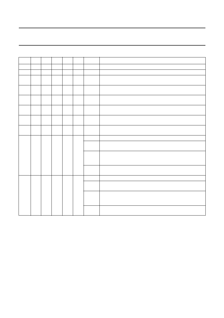
1999 Apr 14
42
Philips Semiconductors
Product specification
Audio processor with head amplifier for VHS hi-fi
TDA9605H
Table 41 Test modes for evaluation and measurement purposes
Notes
1. This test can be used with a HIGH-level input signal by setting bit HPD = 1; test input signal applied to pin HMSW.
2. Auto-normal is activated (bit AUTN = 1) during the test, i.e. the playback audio signal is not available.
3. The output level on pin ENVOUT shows 6 dB attenuation compared to the internal signal of the head amplifier output.
4. This test connects internal signal lines between the noise reduction and (de-)modulator circuit. The signals found
here are not compensated for temperature or tolerance spread and therefore level measurements are only relative.
Absolute values are not an indication of the overall performance. Typical audio level of the test inputs and outputs is
approximately
-
6.5 dBV for the standard
-
8 dBV line level and 50 kHz FM deviation.
5. The expander test requires the auto-normal function to be set inactive; i.e. an FM carrier signal should be available.
TEST HRL NIL3 NIL2 NIL1 NIL0
MODE
DESCRIPTION
1
0
0
0
0
1
test 1
record mode; left channel FM carrier only (1.3 or 1.4 MHz)
1
0
0
0
1
0
test 2
record mode; right channel FM carrier only (1.7 or 1.8 MHz)
1
0
0
0
1
1
test 3
playback mode; left channel band-pass filter with HF AGC off;
EOS = 1 (test output on pin ENVOUT); notes 1 and 2
1
0
0
1
0
0
test 4
playback mode; right channel band-pass filter with HF AGC off;
EOS = 1 (test output on pin ENVOUT); notes 1 and 2
1
0
0
1
0
1
test 5
playback mode; HF AGC (left channel band-pass filter);
EOS = 1 (test output on pin ENVOUT); notes 1 and 2
1
0
0
1
1
0
test 6
playback mode; HF AGC (right channel band-pass filter);
EOS = 1 (test output on pin ENVOUT); notes 1 and 2
1
0
1
0
0
0
test 8
playback mode; head amplifier output signal;
EOS = 1 (test output on pin ENVOUT; notes 2 and 3
1
0
1
0
1
0
test 10
playback mode; HF envelope of right channel carrier;
EOS = 1 (test output on pin ENVOUT)
1
1
1
0
0
1
test 25
noise reduction and modem; note 4
test 25a left channel FM modulator (left carrier only);
record mode; volume setting =
-
3 dB; test input = line input left
test 25b left and right noise reduction (compressor);
record mode; output select function = mute;
test output = line output
test 25c left and right channel FM demodulator; playback mode;
output select function = mute; test output = line output
1
1
1
0
1
0
test 26
noise reduction and modem; note 4
test 26a right channel FM modulator (right carrier only);
record mode; volume setting =
-
3 dB; test input = line input right
test 26b left and right channel audio lowpass filter; record mode;
volume setting =
-
3 dB; output select function = mute;
test input = line input; test output = line output
test 26c left and right channel noise reduction (expander); playback mode;
volume setting =
-
3 dB; test input = line input; note 5
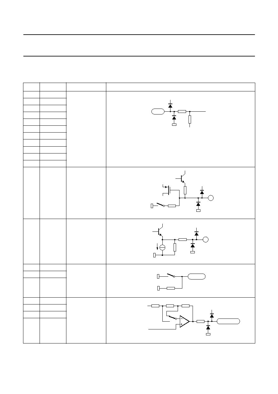
1999 Apr 14
43
Philips Semiconductors
Product specification
Audio processor with head amplifier for VHS hi-fi
TDA9605H
15 INTERNAL CIRCUITRY
The indicated DC voltages are given for the record-mute mode in the typical application circuit without audio signal;
unless otherwise specified.
PIN
SYMBOL
VOLTAGE
EQUIVALENT CIRCUIT
1
SAP
3.8 V
2
TUNL
3
TUNR
4
CINL
5
CINR
6
EXT1L
7
EXT1R
8
EXT2L
9
EXT2R
10
AUXL
11
AUXR
12
RFCAGC
0 V
13
RFCOUT
3.8 V
14
MUTEC
0 V
15
MUTEL
18
MUTER
16
LINEL
4.5 V (VCCS = 0);
6 V (VCCS = 1)
17
LINER
19
DECL
20
DECR
MGR849
73 k
57 k
1 to 11
3.8 V
VCC
MGR850
100
500
12
VCC
bit RFCM
180 k
200
13
VCC
230
µ
A
MGR851
MGR852
100 k
14, 15, 18
bit MUTE or VCC
<
7 V
100
20 k
2.8 k
22.8 k
VCC
class AB
bit VCCS VCC
MGR853
16, 17, 19, 20
bit LOH
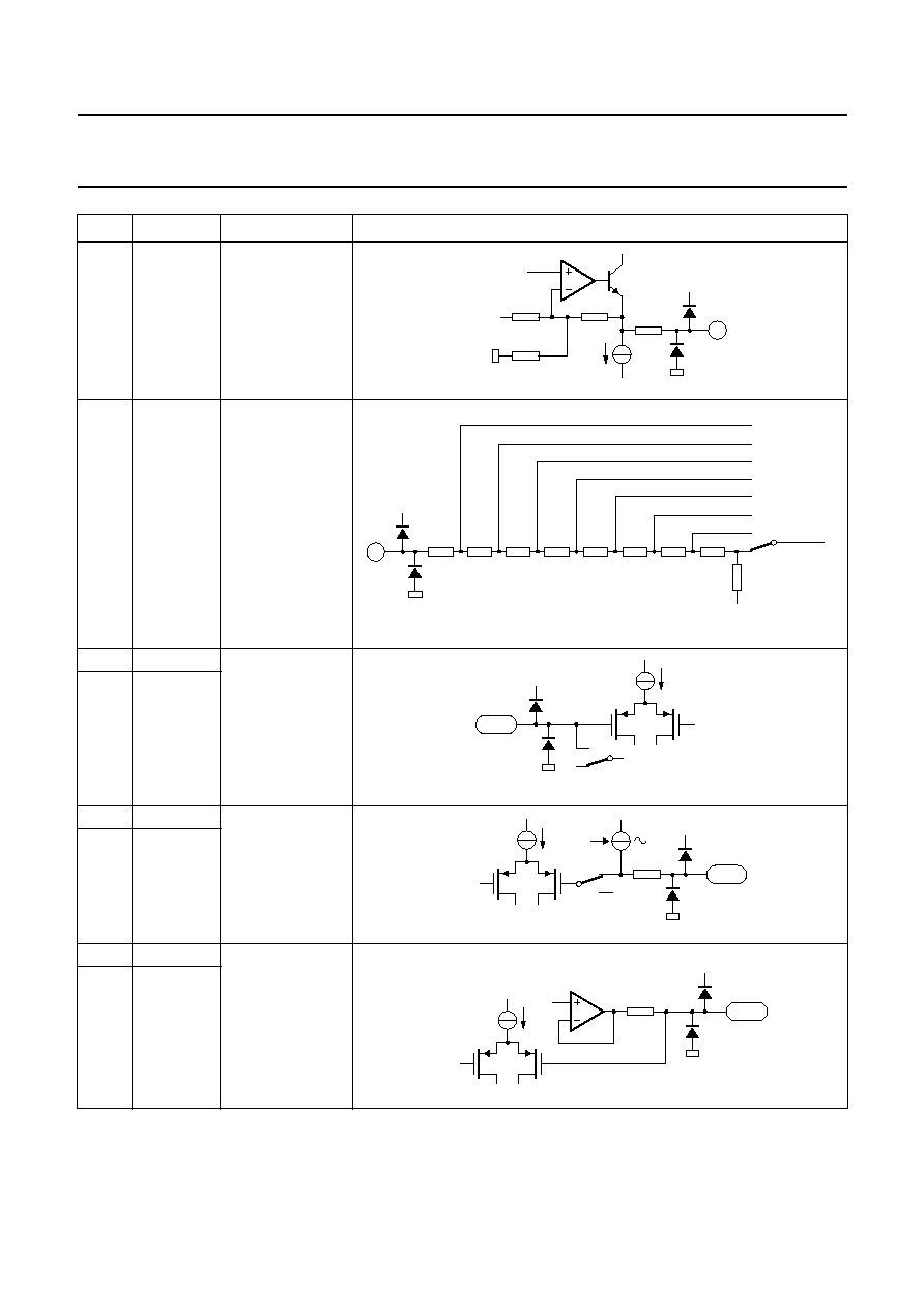
1999 Apr 14
44
Philips Semiconductors
Product specification
Audio processor with head amplifier for VHS hi-fi
TDA9605H
21
LINOUT
4.5 V
22
LININ
3.8 V
23
DCFBL
3.8 V
33
DCFBR
24
EMPHL
3.8 V
32
EMPHR
25
DCL
3.8 V
31
DCR
PIN
SYMBOL
VOLTAGE
EQUIVALENT CIRCUIT
MGR854
200
17.7 k
30 k
21
VCC
600
µ
A
3.8 V
96.4 k
MGR855
total = 130 k
3.8 V
22
VCC
bits NIL2 to NIL0
3.8 V
MGR856
bit AFM
23, 33
VCC
MGR857
240
24, 32
VCC
3.8 V
bit AFM
MGR858
2.8 k
25, 31
VCC
3.8 V
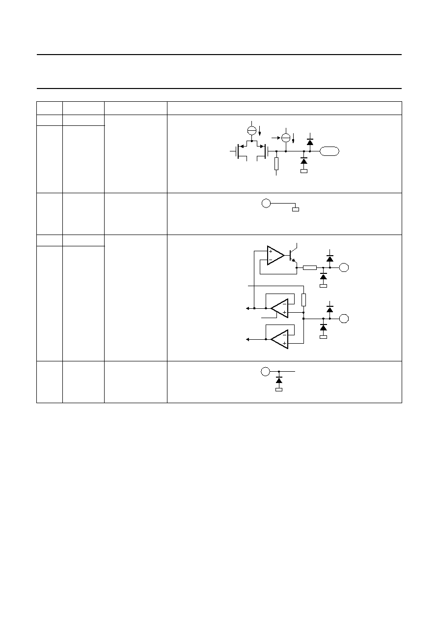
1999 Apr 14
45
Philips Semiconductors
Product specification
Audio processor with head amplifier for VHS hi-fi
TDA9605H
26
DETL
0.7 V
30
DETR
27
GND
0 V
28
I
ref
3.8 V
29
V
ref
34
V
CC
9 to 12 V
PIN
SYMBOL
VOLTAGE
EQUIVALENT CIRCUIT
MGR859
26, 30
VCC
0.5 V
7.5 k
27
substrate
MGR860
200
28
VCC
20
k
3.8 V from
reference
generator
(3.8
-
a) V
3.8 V
29
VCC
MGR861
bit STBA
bit STBP
MGR862
VCC
34

1999 Apr 14
46
Philips Semiconductors
Product specification
Audio processor with head amplifier for VHS hi-fi
TDA9605H
35
PBIN2
0.7 V;
4.3 V (recording)
36
RECOUT
37
PBIN1
38
HMSW
0 V;
4.3 V (recording)
39
GNDH
0 V
40
V
CCH
5 V
PIN
SYMBOL
VOLTAGE
EQUIVALENT CIRCUIT
signal RM
playback or
record-mute
mode
GNDH
VCC
VCCH
35
k
5
GNDH
GNDH
35
36
to HF AGC
MGR863
VCC
VCCH
35
k
GNDH
GNDH
37
38
&
&
bit AFM
bit HPD
bit DOC
bit SHH
bit DETH
GNDH
39
MGR864
VCCH
40
MGR865
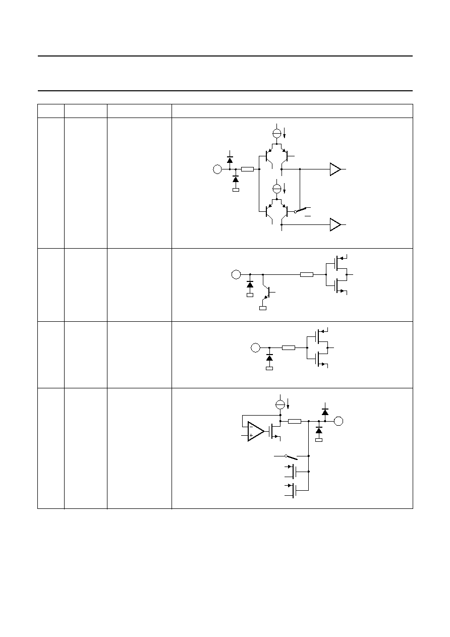
1999 Apr 14
47
Philips Semiconductors
Product specification
Audio processor with head amplifier for VHS hi-fi
TDA9605H
41
RMHID
0 to 5 V
42
SDA
0 or 5 V
43
SCL
0 or 5 V
44
ENVOUT
0 V
PIN
SYMBOL
VOLTAGE
EQUIVALENT CIRCUIT
3 k
MGR866
2.5 V
0.8 V
4.05 V
signal RM
signal HID
41
VCC
42
MGR867
275
bit ACK
(I
2
C-bus acknowledge)
43
MGR868
275
1 k
44
VCC
test modes
40
µ
A
MGR869
1999 Apr 14
48
Philips Semiconductors
Product specification
Audio processor with head amplifier for VHS hi-fi
TDA9605H
16 PACKAGE OUTLINE
UNIT
A
1
A
2
A
3
b
p
c
E
(1)
e
H
E
L
L
p
Z
y
w
v
REFERENCES
OUTLINE
VERSION
EUROPEAN
PROJECTION
ISSUE DATE
IEC
JEDEC
EIAJ
mm
0.25
0.05
1.85
1.65
0.25
0.40
0.20
0.25
0.14
10.1
9.9
0.8
1.3
12.9
12.3
1.2
0.8
10
0
o
o
0.15
0.1
0.15
DIMENSIONS (mm are the original dimensions)
Note
1. Plastic or metal protrusions of 0.25 mm maximum per side are not included.
0.95
0.55
SOT307-2
95-02-04
97-08-01
D
(1)
(1)
(1)
10.1
9.9
H
D
12.9
12.3
E
Z
1.2
0.8
D
e
E
B
11
c
E
H
D
ZD
A
Z E
e
v
M
A
X
1
44
34
33
23
22
12
y
A
1
A
L
p
detail X
L
(A )
3
A
2
pin 1 index
D
H
v
M
B
b
p
b
p
w
M
w
M
0
2.5
5 mm
scale
QFP44: plastic quad flat package; 44 leads (lead length 1.3 mm); body 10 x 10 x 1.75 mm
SOT307-2
A
max.
2.10

1999 Apr 14
49
Philips Semiconductors
Product specification
Audio processor with head amplifier for VHS hi-fi
TDA9605H
17 SOLDERING
17.1
Introduction to soldering surface mount
packages
This text gives a very brief insight to a complex technology.
A more in-depth account of soldering ICs can be found in
our
"Data Handbook IC26; Integrated Circuit Packages"
(document order number 9398 652 90011).
There is no soldering method that is ideal for all surface
mount IC packages. Wave soldering is not always suitable
for surface mount ICs, or for printed-circuit boards with
high population densities. In these situations reflow
soldering is often used.
17.2
Reflow soldering
Reflow soldering requires solder paste (a suspension of
fine solder particles, flux and binding agent) to be applied
to the printed-circuit board by screen printing, stencilling or
pressure-syringe dispensing before package placement.
Several methods exist for reflowing; for example,
infrared/convection heating in a conveyor type oven.
Throughput times (preheating, soldering and cooling) vary
between 100 and 200 seconds depending on heating
method.
Typical reflow peak temperatures range from
215 to 250
∞
C. The top-surface temperature of the
packages should preferable be kept below 230
∞
C.
17.3
Wave soldering
Conventional single wave soldering is not recommended
for surface mount devices (SMDs) or printed-circuit boards
with a high component density, as solder bridging and
non-wetting can present major problems.
To overcome these problems the double-wave soldering
method was specifically developed.
If wave soldering is used the following conditions must be
observed for optimal results:
∑
Use a double-wave soldering method comprising a
turbulent wave with high upward pressure followed by a
smooth laminar wave.
∑
For packages with leads on two sides and a pitch (e):
≠ larger than or equal to 1.27 mm, the footprint
longitudinal axis is preferred to be parallel to the
transport direction of the printed-circuit board;
≠ smaller than 1.27 mm, the footprint longitudinal axis
must be parallel to the transport direction of the
printed-circuit board.
The footprint must incorporate solder thieves at the
downstream end.
∑
For packages with leads on four sides, the footprint must
be placed at a 45
∞
angle to the transport direction of the
printed-circuit board. The footprint must incorporate
solder thieves downstream and at the side corners.
During placement and before soldering, the package must
be fixed with a droplet of adhesive. The adhesive can be
applied by screen printing, pin transfer or syringe
dispensing. The package can be soldered after the
adhesive is cured.
Typical dwell time is 4 seconds at 250
∞
C.
A mildly-activated flux will eliminate the need for removal
of corrosive residues in most applications.
17.4
Manual soldering
Fix the component by first soldering two
diagonally-opposite end leads. Use a low voltage (24 V or
less) soldering iron applied to the flat part of the lead.
Contact time must be limited to 10 seconds at up to
300
∞
C.
When using a dedicated tool, all other leads can be
soldered in one operation within 2 to 5 seconds between
270 and 320
∞
C.

1999 Apr 14
50
Philips Semiconductors
Product specification
Audio processor with head amplifier for VHS hi-fi
TDA9605H
17.5
Suitability of surface mount IC packages for wave and reflow soldering methods
Notes
1. All surface mount (SMD) packages are moisture sensitive. Depending upon the moisture content, the maximum
temperature (with respect to time) and body size of the package, there is a risk that internal or external package
cracks may occur due to vaporization of the moisture in them (the so called popcorn effect). For details, refer to the
Drypack information in the
"Data Handbook IC26; Integrated Circuit Packages; Section: Packing Methods".
2. These packages are not suitable for wave soldering as a solder joint between the printed-circuit board and heatsink
(at bottom version) can not be achieved, and as solder may stick to the heatsink (on top version).
3. If wave soldering is considered, then the package must be placed at a 45
∞
angle to the solder wave direction.
The package footprint must incorporate solder thieves downstream and at the side corners.
4. Wave soldering is only suitable for LQFP, TQFP and QFP packages with a pitch (e) equal to or larger than 0.8 mm;
it is definitely not suitable for packages with a pitch (e) equal to or smaller than 0.65 mm.
5. Wave soldering is only suitable for SSOP and TSSOP packages with a pitch (e) equal to or larger than 0.65 mm; it is
definitely not suitable for packages with a pitch (e) equal to or smaller than 0.5 mm.
PACKAGE
SOLDERING METHOD
WAVE
REFLOW
(1)
BGA, SQFP
not suitable
suitable
HLQFP, HSQFP, HSOP, HTSSOP, SMS not suitable
(2)
suitable
PLCC
(3)
, SO, SOJ
suitable
suitable
LQFP, QFP, TQFP
not recommended
(3)(4)
suitable
SSOP, TSSOP, VSO
not recommended
(5)
suitable
1999 Apr 14
51
Philips Semiconductors
Product specification
Audio processor with head amplifier for VHS hi-fi
TDA9605H
18 DEFINITIONS
19 LIFE SUPPORT APPLICATIONS
These products are not designed for use in life support appliances, devices, or systems where malfunction of these
products can reasonably be expected to result in personal injury. Philips customers using or selling these products for
use in such applications do so at their own risk and agree to fully indemnify Philips for any damages resulting from such
improper use or sale.
20 PURCHASE OF PHILIPS I
2
C COMPONENTS
Data sheet status
Objective specification
This data sheet contains target or goal specifications for product development.
Preliminary specification
This data sheet contains preliminary data; supplementary data may be published later.
Product specification
This data sheet contains final product specifications.
Limiting values
Limiting values given are in accordance with the Absolute Maximum Rating System (IEC 134). Stress above one or
more of the limiting values may cause permanent damage to the device. These are stress ratings only and operation
of the device at these or at any other conditions above those given in the Characteristics sections of the specification
is not implied. Exposure to limiting values for extended periods may affect device reliability.
Application information
Where application information is given, it is advisory and does not form part of the specification.
Purchase of Philips I
2
C components conveys a license under the Philips I
2
C patent to use the
components in the I
2
C system provided the system conforms to the I
2
C specification defined by
Philips. This specification can be ordered using the code 9398 393 40011.

Internet: http://www.semiconductors.philips.com
Philips Semiconductors ≠ a worldwide company
© Philips Electronics N.V. 1999
SCA63
All rights are reserved. Reproduction in whole or in part is prohibited without the prior written consent of the copyright owner.
The information presented in this document does not form part of any quotation or contract, is believed to be accurate and reliable and may be changed
without notice. No liability will be accepted by the publisher for any consequence of its use. Publication thereof does not convey nor imply any license
under patent- or other industrial or intellectual property rights.
Netherlands: Postbus 90050, 5600 PB EINDHOVEN, Bldg. VB,
Tel. +31 40 27 82785, Fax. +31 40 27 88399
New Zealand: 2 Wagener Place, C.P.O. Box 1041, AUCKLAND,
Tel. +64 9 849 4160, Fax. +64 9 849 7811
Norway: Box 1, Manglerud 0612, OSLO,
Tel. +47 22 74 8000, Fax. +47 22 74 8341
Pakistan: see Singapore
Philippines: Philips Semiconductors Philippines Inc.,
106 Valero St. Salcedo Village, P.O. Box 2108 MCC, MAKATI,
Metro MANILA, Tel. +63 2 816 6380, Fax. +63 2 817 3474
Poland: Ul. Lukiska 10, PL 04-123 WARSZAWA,
Tel. +48 22 612 2831, Fax. +48 22 612 2327
Portugal: see Spain
Romania: see Italy
Russia: Philips Russia, Ul. Usatcheva 35A, 119048 MOSCOW,
Tel. +7 095 755 6918, Fax. +7 095 755 6919
Singapore: Lorong 1, Toa Payoh, SINGAPORE 319762,
Tel. +65 350 2538, Fax. +65 251 6500
Slovakia: see Austria
Slovenia: see Italy
South Africa: S.A. PHILIPS Pty Ltd., 195-215 Main Road Martindale,
2092 JOHANNESBURG, P.O. Box 7430 Johannesburg 2000,
Tel. +27 11 470 5911, Fax. +27 11 470 5494
South America: Al. Vicente Pinzon, 173, 6th floor,
04547-130 S√O PAULO, SP, Brazil,
Tel. +55 11 821 2333, Fax. +55 11 821 2382
Spain: Balmes 22, 08007 BARCELONA,
Tel. +34 93 301 6312, Fax. +34 93 301 4107
Sweden: Kottbygatan 7, Akalla, S-16485 STOCKHOLM,
Tel. +46 8 5985 2000, Fax. +46 8 5985 2745
Switzerland: Allmendstrasse 140, CH-8027 ZÐRICH,
Tel. +41 1 488 2741 Fax. +41 1 488 3263
Taiwan: Philips Semiconductors, 6F, No. 96, Chien Kuo N. Rd., Sec. 1,
TAIPEI, Taiwan Tel. +886 2 2134 2886, Fax. +886 2 2134 2874
Thailand: PHILIPS ELECTRONICS (THAILAND) Ltd.,
209/2 Sanpavuth-Bangna Road Prakanong, BANGKOK 10260,
Tel. +66 2 745 4090, Fax. +66 2 398 0793
Turkey: Talatpasa Cad. No. 5, 80640 GÐLTEPE/ISTANBUL,
Tel. +90 212 279 2770, Fax. +90 212 282 6707
Ukraine: PHILIPS UKRAINE, 4 Patrice Lumumba str., Building B, Floor 7,
252042 KIEV, Tel. +380 44 264 2776, Fax. +380 44 268 0461
United Kingdom: Philips Semiconductors Ltd., 276 Bath Road, Hayes,
MIDDLESEX UB3 5BX, Tel. +44 181 730 5000, Fax. +44 181 754 8421
United States: 811 East Arques Avenue, SUNNYVALE, CA 94088-3409,
Tel. +1 800 234 7381, Fax. +1 800 943 0087
Uruguay: see South America
Vietnam: see Singapore
Yugoslavia: PHILIPS, Trg N. Pasica 5/v, 11000 BEOGRAD,
Tel. +381 11 62 5344, Fax.+381 11 63 5777
For all other countries apply to: Philips Semiconductors,
International Marketing & Sales Communications, Building BE-p, P.O. Box 218,
5600 MD EINDHOVEN, The Netherlands, Fax. +31 40 27 24825
Argentina: see South America
Australia: 34 Waterloo Road, NORTH RYDE, NSW 2113,
Tel. +61 2 9805 4455, Fax. +61 2 9805 4466
Austria: Computerstr. 6, A-1101 WIEN, P.O. Box 213,
Tel. +43 1 60 101 1248, Fax. +43 1 60 101 1210
Belarus: Hotel Minsk Business Center, Bld. 3, r. 1211, Volodarski Str. 6,
220050 MINSK, Tel. +375 172 20 0733, Fax. +375 172 20 0773
Belgium: see The Netherlands
Brazil: see South America
Bulgaria: Philips Bulgaria Ltd., Energoproject, 15th floor,
51 James Bourchier Blvd., 1407 SOFIA,
Tel. +359 2 68 9211, Fax. +359 2 68 9102
Canada: PHILIPS SEMICONDUCTORS/COMPONENTS,
Tel. +1 800 234 7381, Fax. +1 800 943 0087
China/Hong Kong: 501 Hong Kong Industrial Technology Centre,
72 Tat Chee Avenue, Kowloon Tong, HONG KONG,
Tel. +852 2319 7888, Fax. +852 2319 7700
Colombia: see South America
Czech Republic: see Austria
Denmark: Sydhavnsgade 23, 1780 COPENHAGEN V,
Tel. +45 33 29 3333, Fax. +45 33 29 3905
Finland: Sinikalliontie 3, FIN-02630 ESPOO,
Tel. +358 9 615 800, Fax. +358 9 6158 0920
France: 51 Rue Carnot, BP317, 92156 SURESNES Cedex,
Tel. +33 1 4099 6161, Fax. +33 1 4099 6427
Germany: Hammerbrookstraþe 69, D-20097 HAMBURG,
Tel. +49 40 2353 60, Fax. +49 40 2353 6300
Hungary: see Austria
India: Philips INDIA Ltd, Band Box Building, 2nd floor,
254-D, Dr. Annie Besant Road, Worli, MUMBAI 400 025,
Tel. +91 22 493 8541, Fax. +91 22 493 0966
Indonesia: PT Philips Development Corporation, Semiconductors Division,
Gedung Philips, Jl. Buncit Raya Kav.99-100, JAKARTA 12510,
Tel. +62 21 794 0040 ext. 2501, Fax. +62 21 794 0080
Ireland: Newstead, Clonskeagh, DUBLIN 14,
Tel. +353 1 7640 000, Fax. +353 1 7640 200
Israel: RAPAC Electronics, 7 Kehilat Saloniki St, PO Box 18053,
TEL AVIV 61180, Tel. +972 3 645 0444, Fax. +972 3 649 1007
Italy: PHILIPS SEMICONDUCTORS, Piazza IV Novembre 3,
20124 MILANO, Tel. +39 2 6752 2531, Fax. +39 2 6752 2557
Japan: Philips Bldg 13-37, Kohnan 2-chome, Minato-ku,
TOKYO 108-8507, Tel. +81 3 3740 5130, Fax. +81 3 3740 5077
Korea: Philips House, 260-199 Itaewon-dong, Yongsan-ku, SEOUL,
Tel. +82 2 709 1412, Fax. +82 2 709 1415
Malaysia: No. 76 Jalan Universiti, 46200 PETALING JAYA, SELANGOR,
Tel. +60 3 750 5214, Fax. +60 3 757 4880
Mexico: 5900 Gateway East, Suite 200, EL PASO, TEXAS 79905,
Tel. +9-5 800 234 7381, Fax +9-5 800 943 0087
Middle East: see Italy
Printed in The Netherlands
545004/750/01/pp52
Date of release: 1999 Apr 14
Document order number:
9397 750 04687