 | –≠–ª–µ–∫—Ç—Ä–æ–Ω–Ω—ã–π –∫–æ–º–ø–æ–Ω–µ–Ω—Ç: TDA9806 | –°–∫–∞—á–∞—Ç—å:  PDF PDF  ZIP ZIP |

DATA SHEET
Preliminary specification
File under Integrated Circuits, IC02
1995 Sep 05
INTEGRATED CIRCUITS
TDA9806
Multistandard VIF-PLL and
FM-PLL demodulator

1995 Sep 05
2
Philips Semiconductors
Preliminary specification
Multistandard VIF-PLL and
FM-PLL demodulator
TDA9806
FEATURES
∑
5 V supply voltage
∑
Gain controlled wide band VIF-amplifier (AC-coupled)
∑
True synchronous demodulation with active carrier
regeneration (very linear demodulation,
good intermodulation figures, reduced harmonics,
excellent pulse response)
∑
Separate video amplifier for sound trap buffering with
high video bandwidth
∑
VIF AGC detector for gain control, operating as peak
sync detector for B/G
∑
Tuner AGC with adjustable takeover point (TOP)
∑
AFC detector without extra reference circuit
∑
AC-coupled limiter amplifier for sound intercarrier signal
∑
Alignment-free FM-PLL demodulator with high linearity,
switchable de-emphasis for FM
∑
Stabilizer circuit for ripple rejection and to achieve
constant output signals.
GENERAL DESCRIPTION
The TDA9806 is an integrated circuit for multistandard
vision IF signal processing and FM sound demodulation in
TV and VCR sets.
ORDERING INFORMATION
TYPE NUMBER
PACKAGE
NAME
DESCRIPTION
VERSION
TDA9806
SDIP32
plastic shrink dual in-line package; 32 leads (400 mil)
SOT232-1
1995 Sep 05
3
Philips Semiconductors
Preliminary specification
Multistandard VIF-PLL and
FM-PLL demodulator
TDA9806
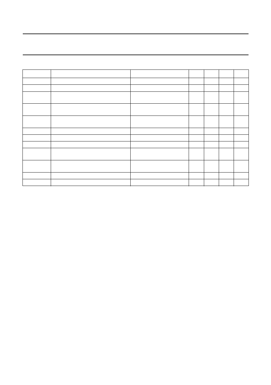
QUICK REFERENCE DATA
SYMBOL
PARAMETER
CONDITIONS
MIN.
TYP.
MAX.
UNIT
V
P
supply voltage
4.5
5
5.5
V
I
P
supply current
82
96
110
mA
V
i VIF(rms)
vision IF input signal voltage sensitivity
(RMS value)
-
1 dB video at output
-
60
100
µ
V
V
o CVBS (p-p)
CVBS output signal voltage
(peak-to-peak value)
1.7
2.0
2.3
V
B
-
3
-
3 dB video bandwidth on pin CVBS
B/G standard; C
L
<
20 pF;
R
L
>
1 k
; AC load
7
8
-
MHz
S/N (W)
weighted signal-to-noise ratio for video
56
60
-
dB
IM
1.1
intermodulation attenuation at `blue'
f = 1.1 MHz
58
64
-
dB
IM
3.3
intermodulation attenuation at `blue'
f = 3.3 MHz
58
64
-
dB
H(sup)
suppression of harmonics in video
signal
35
40
-
dB
V
o(rms)
audio output signal voltage for FM
(RMS value)
B/G standard;
54% modulation
-
0.5
-
V
THD
total harmonic distortion for FM
54% modulation
-
0.15
0.5
%
S/N (W)
weighted signal-to-noise ratio for FM
54% modulation
-
60
-
dB
1995 Sep 05
4
Philips Semiconductors
Preliminary specification
Multistandard VIF-PLL and
FM-PLL demodulator
TDA9806
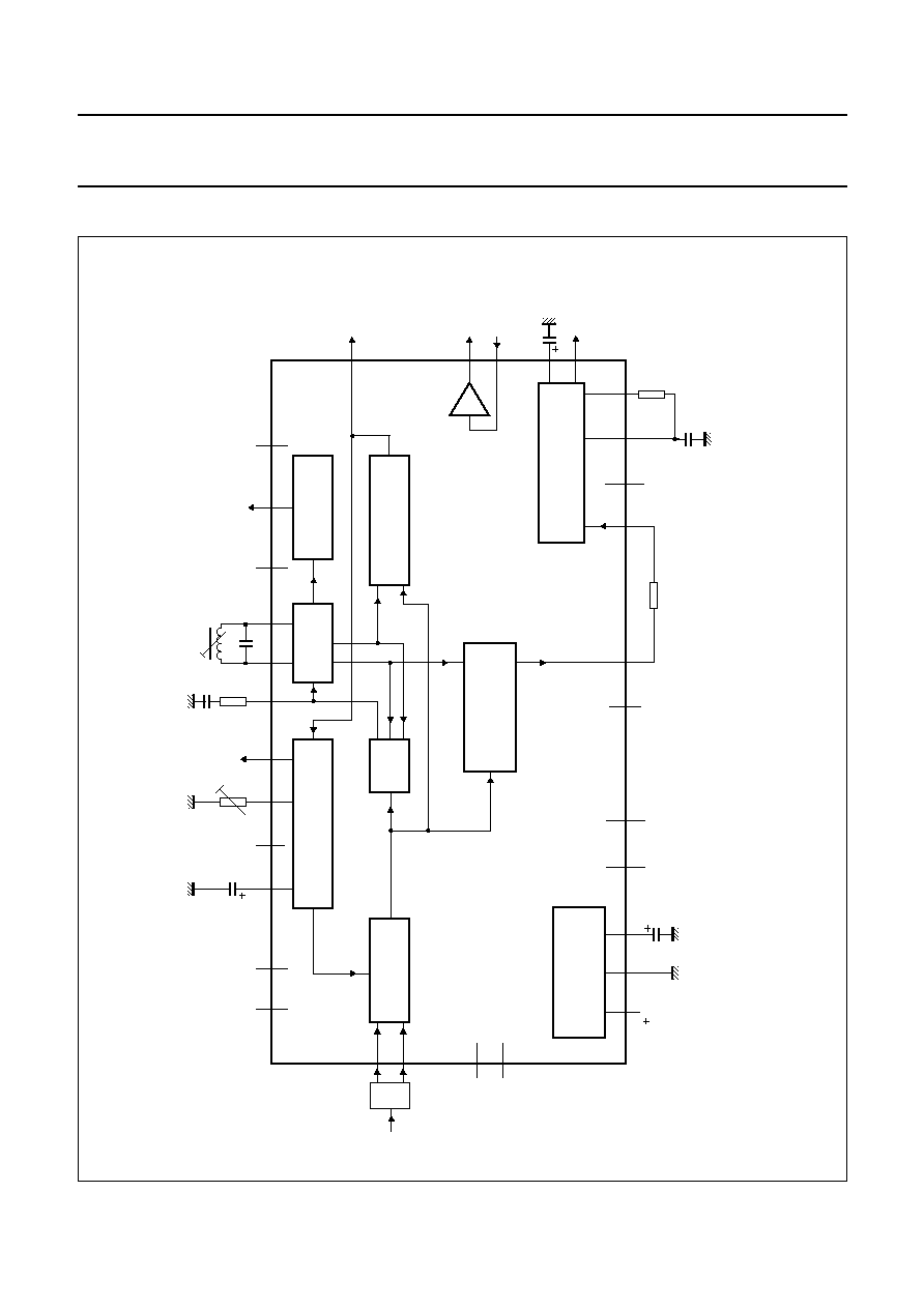
BLOCK DIAGRAM
h
andbook, full pagewidth
INTERCARRIER
MIXER
VCO TWD
AFC DETECTOR
TUNER AND VIF-AGC
FPLL
VIDEO DEMODULATOR
AND AMPLIFIER
INTERNAL VOLTAGE
STABILIZER
FM DETECTOR (PLL)
AF AMPLIFIER
VIF AMPLIFIER
VIF
TDA9806
29
27
26
9
10
21
22
15
12
23
24
25
7
19
28
6
3
2
1
32
31
5 V
VP
1/2
11
20
17
5.5
SIF
14
13
16
n.c.
n.c.
n.c.
8
n.c.
AF
de-emphasis
VIDEO
BUFFER
CVBS
2 V (p-p)
video
1 V (p-p)
AFC
2 x f PC
tuner
AGC
loop
filter
n.c.
4
n.c.
5
n.c.
18
n.c.
30
n.c.
n.c.
n.c.
TOP
CAGC
MHA054
Vi(vid)
Fig.1 Block diagram.
1995 Sep 05
5
Philips Semiconductors
Preliminary specification
Multistandard VIF-PLL and
FM-PLL demodulator
TDA9806
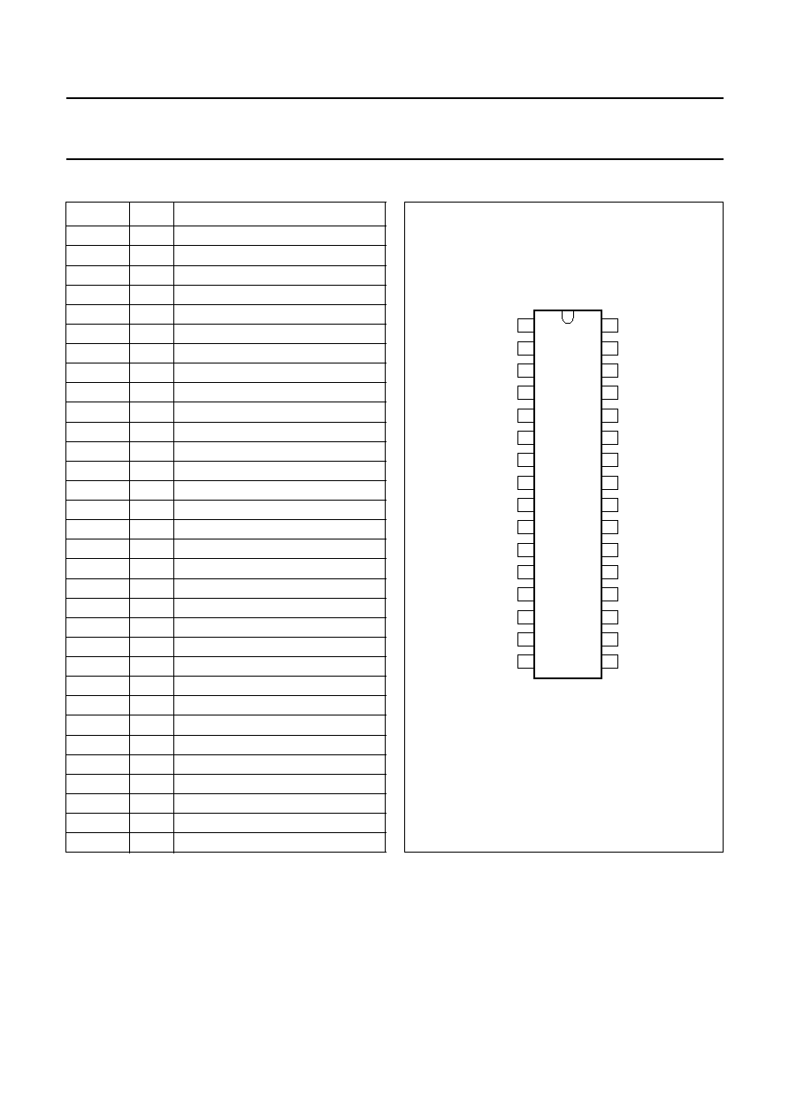
PINNING
SYMBOL
PIN
DESCRIPTION
V
i VIF1
1
VIF differential input signal voltage 1
V
i VIF2
2
VIF differential input signal voltage 2
n.c.
3
not connected
n.c.
4
not connected
n.c.
5
not connected
TADJ
6
tuner AGC takeover adjust (TOP)
T
PLL
7
PLL loop filter
n.c.
8
not connected
n.c.
9
not connected
V
o CVBS
10
CVBS output signal voltage
n.c.
11
not connected
V
o AF
12
audio voltage frequency output
DEEM
I
13
de-emphasis input
DEEM
O
14
de-emphasis output
C
DEC
15
decoupling capacitor
n.c.
16
not connected
V
i FM
17
sound intercarrier input voltage
n.c.
18
not connected
TAGC
19
tuner AGC output
V
o(int)
20
sound intercarrier output voltage
V
o(vid)
21
composite video output voltage
V
i(vid)
22
video buffer input voltage
AFC
23
AFC output
VCO1
24
VCO1 reference circuit for 2f
PC
VCO2
25
VCO2 reference circuit for 2f
PC
C
ref
26
1
/
2
V
P
reference capacitor
GND
27
ground
C
VAGC
28
VIF AGC capacitor
V
P
29
supply voltage
n.c.
30
not connected
n.c.
31
not connected
n.c.
32
not connected
Fig.2 Pin configuration.
handbook, halfpage
TDA9806
MHA053
1
2
3
4
5
6
7
8
9
10
11
12
13
14
15
16
32
31
30
29
28
27
26
25
24
23
22
21
20
19
18
17
V
V
TADJ
T
V
V
n.c.
n.c.
n.c.
n.c.
n.c.
n.c.
n.c.
V
C
GND
n.c.
n.c.
n.c.
C
VCO2
VCO1
AFC
V
V
V
TAGC
n.c.
o AF
DEEM I
DEEM O
C DEC
o CVBS
PLL
i VIF2
i VIF1
P
VAGC
ref
Vi FM
o(int)
o(vid)
i(vid)

1995 Sep 05
6
Philips Semiconductors
Preliminary specification
Multistandard VIF-PLL and
FM-PLL demodulator
TDA9806
FUNCTIONAL DESCRIPTION
Vision IF amplifier
The vision IF amplifier consists of three AC-coupled
differential amplifier stages. Each differential stage
comprises a feedback network controlled by emitter
degeneration.
Tuner and VIF AGC
The AGC capacitor voltage is transferred to an internal IF
control signal, and is fed to the tuner AGC to generate the
tuner AGC output current (open-collector output). The
tuner AGC takeover point can be adjusted. This allows the
tuner and the SWIF filter to be matched to achieve the
optimum IF input level.
The AGC detector charges/discharges the AGC capacitor
to the required voltage for setting of VIF and tuner gain in
order to keep the video signal at a constant level.
Therefore for negative video modulation the sync level of
the video signal is detected.
Frequency Phase Locked Loop detector (FPLL)
The VIF-amplifier output signal is fed into a frequency
detector and into a phase detector via a limiting amplifier.
During acquisition the frequency detector produces a DC
current proportional to the frequency difference between
the input and the VCO signal. After frequency lock-in the
phase detector produces a DC current proportional to the
phase difference between the VCO and the input signal.
The DC current of either frequency detector or phase
detector is converted into a DC voltage via the loop filter,
which controls the VCO frequency.
VCO, travelling wave divider and AFC
The VCO operates with a resonance circuit (with L and C
in parallel) at double the PC frequency. The VCO is
controlled by two integrated variable capacitors. The
control voltage required to tune the VCO from its
free-running frequency to actually double the PC
frequency is generated by the Frequency-Phase detector
and fed via the loop filter to the first variable capacitor
(FPLL). This control voltage is amplified and additionally
converted into a current which represents the AFC output
signal. At centre frequency the AFC output current is equal
to zero.
The oscillator signal is divided-by-two with a Travelling
Wave Divider (TWD) which generates two differential
output signals with a 90 degree phase difference
independent of the frequency.
Video demodulator and amplifier
The video demodulator is realized by a multiplier which is
designed for low distortion and large bandwidth. The vision
IF input signal is multiplied with the `in-phase' signal of the
travelling wave divider output.
The demodulator output signal is fed via an integrated
low-pass filter for attenuation of the carrier harmonics to
the video amplifier. The video amplifier is realized by an
operational amplifier with internal feedback and high
bandwidth. A low-pass filter is integrated to achieve an
attenuation of the carrier harmonics. The video output
signal is 1 V (p-p) for nominal vision IF modulation.
Video buffer
For an easy adaption of the sound traps an operational
amplifier with internal feedback is used. This amplifier is
featured with a high bandwidth and 7 dB gain. The input
impedance is adapted for operating in combination with
ceramic sound traps. The output stage delivers a nominal
2 V (p-p) positive video signal. Noise clipping is provided.
Intercarrier mixer
The intercarrier mixer is realized by a multiplier. The VIF
amplifier output signal is fed to the intercarrier mixer and
converted to intercarrier frequency by the regenerated
picture carrier (VCO). The mixer output signal is fed via a
high-pass for attenuation of the video signal components.

1995 Sep 05
7
Philips Semiconductors
Preliminary specification
Multistandard VIF-PLL and
FM-PLL demodulator
TDA9806
FM detector
The FM detector consists of a limiter, an FM-PLL and an
AF amplifier. The limiter provides the amplification and
limitation of the FM sound intercarrier signal before
demodulation. The result is high sensitivity and AM
suppression. The amplifier consists of 7 stages which are
internally AC-coupled in order to minimize the DC offset
and to save pins for DC decoupling.
The FM-PLL consists of an integrated relaxation oscillator,
an integrated loop filter and a phase detector. The
oscillator is locked to the FM intercarrier signal, output
from the limiter. As a result of locking, the oscillator
frequency tracks with the modulation of the input signal
and the oscillator control voltage is superimposed by the
AF voltage. The FM-PLL operates as an FM-demodulator.
The AF amplifier consists of two parts:
1. The AF preamplifier for FM sound is an operational
amplifier with internal feedback, high gain and high
common mode rejection. The AF voltage from the PLL
demodulator, by principle a small output signal, is
amplified by approximately 33 dB. The low-pass
characteristic of the amplifier reduces the harmonics of
the intercarrier signal at the sound output terminal, at
which the de-emphasis network for FM sound is
applied. An additional DC control circuit is
implemented to keep the DC level constant,
independent of process spread.
2. The AF output amplifier (10 dB) provides the required
output level by a rail-to-rail output stage. This amplifier
makes use of an input selector for switching to FM
de-emphasis or mute state, controlled by the mute
switching voltage.
Internal voltage stabilizer and
1
/
2
V
P
-reference
The bandgap circuit internally generates a voltage of
approximately 1.25 V, independent of supply voltage and
temperature. A voltage regulator circuit, connected to this
voltage, produces a constant voltage of 3.6 V which is
used as an internal reference voltage.
For all audio output signals the constant reference voltage
cannot be used because large output signals are required.
Therefore these signals refer to half the supply voltage to
achieve a symmetrical headroom, especially for the
rail-to-rail output stage. For ripple and noise attenuation
the
1
/
2
V
P
voltage has to be filtered via a low-pass filter by
using an external capacitor together with an integrated
resistor (f
g
= 5 Hz). For a fast setting to
1
/
2
V
P
an internal
start-up circuit is added.

1995 Sep 05
8
Philips Semiconductors
Preliminary specification
Multistandard VIF-PLL and
FM-PLL demodulator
TDA9806
LIMITING VALUES
In accordance with the Absolute Maximum Rating System (IEC 134).
Notes
1. I
P
= 110 mA; T
amb
= 70
∞
C; R
th j-a
= 60 K/W.
2. Charge device model class B: equivalent to discharging a 200 pF capacitor via a 0
series resistor.
THERMAL CHARACTERISTICS
SYMBOL
PARAMETER
CONDITIONS
MIN.
MAX.
UNIT
V
P
supply voltage (pin 29)
maximum chip temperature
of 120
∞
C; note 1
0
5.5
V
V
i
voltage at pins 1 to 7, 12 to 19, 22, 23, 28
and 29
0
V
P
V
t
s(max)
maximum short-circuit time
-
10
s
V
19
tuner AGC output voltage
0
13.2
V
T
stg
storage temperature
-
25
+150
∞
C
T
amb
operating ambient temperature
-
20
+70
∞
C
V
es
electrostatic handling voltage
note 2
-
300
+
300
V
SYMBOL
PARAMETER
VALUE
UNIT
R
th j-a
thermal resistance from junction to ambient in free air
60
K/W

1995 Sep 05
9
Philips Semiconductors
Preliminary specification
Multistandard VIF-PLL and
FM-PLL demodulator
TDA9806
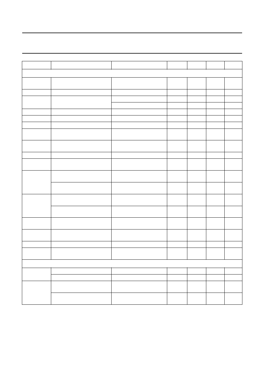
CHARACTERISTICS
V
P
= 5 V; T
amb
= 25
∞
C; see Table 1 for input frequencies and level; input level V
i IF 1, 2
= 10 mV RMS value (sync-level
for B/G); video modulation DSB; residual carrier B/G: 10%; video signal in accordance with
"CCIR, line 17";
measurements taken in Fig.10; unless otherwise specified.
SYMBOL
PARAMETER
CONDITIONS
MIN.
TYP.
MAX.
UNIT
Supply (pin 29)
V
P
supply voltage
note 1
4.5
5
5.5
V
I
P
supply current
82
96
110
mA
Vision IF amplifier (pins 1 and 2)
V
i VIF(rms)
input signal voltage sensitivity
(RMS value)
B/G standard;
-
1 dB video at output
-
60
100
µ
V
V
i max(rms)
maximum input signal voltage
(RMS value)
B/G standard;
+1 dB video at output
120
200
-
mV
V
o(int)
internal IF amplitude difference
between picture and sound
carrier
within AGC range;
B/G standard;
f = 5.5 MHz
-
0.7
1
dB
G
IFcr
IF gain control range
see Fig.3
65
70
-
dB
R
i(diff)
differential input resistance
note 2
1.7
2.2
2.7
k
C
i(diff)
differential input capacitance
note 2
1.2
1.7
2.5
pF
V
1,2
DC input voltage
-
3.4
-
V
True synchronous video demodulator; note 3
f
VCO(max)
maximum oscillator frequency
for carrier regeneration
f = 2f
PC
125
130
-
MHz
f
osc
/
T
oscillator drift as a function of
temperature
oscillator is free-running;
I
AFC
= 0; note 4
-
-
±
20
ppm/K
V
0 ref(rms)
oscillator voltage swing at
pins 24 and 25 (RMS value)
B/G standard
70
100
130
mV
f
pcCR
picture carrier capture range
B/G standard
±
1.5
±
2.0
-
MHz
t
acq
acquisition time
BL = 60 kHz; note 5
-
-
30
ms
V
i VIF(rms)
VIF input signal voltage
sensitivity for PLL to be locked
(RMS value; pins 1 and 2)
maximum IF gain; note 6
-
30
70
µ
V
I
FPLL(offset)
FPLL offset current at pin 7
note 7
-
-
±
4.5
µ
A

1995 Sep 05
10
Philips Semiconductors
Preliminary specification
Multistandard VIF-PLL and
FM-PLL demodulator
TDA9806
Composite video amplifier (pin 21; sound carrier off)
V
o video(p-p)
output signal voltage
(peak-to-peak value)
see Fig.7
0.88
1.0
1.12
V
V
21(sync)
sync voltage level
B/G standard
-
1.5
-
V
V
21(clu)
upper video clipping voltage
level
V
P
-
1.1
V
P
-
1
-
V
V
21(cll)
lower video clipping voltage
level
-
0.3
0.4
V
R
o,21
output resistance
note 2
-
-
10
I
int 21
internal DC bias current for
emitter-follower
1.6
2.0
-
mA
I
21 max(sink)
maximum AC and DC output
sink current
1.0
-
-
mA
I
21 max(source)
maximum AC and DC output
source current
2.0
-
-
mA
B
-
1
-
1 dB video bandwidth
B/G standard; C
L
<
50 pF;
R
L
>
1 k
;
AC load
5
6
-
MHz
B
-
3
-
3 dB video bandwidth
B/G standard; C
L
<
50 pF;
R
L
>
1 k
;
AC load
7
8
-
MHz
H
suppression of video signal
harmonics
C
L
<
50 pF; R
L
>
1 k
;
AC load; note 8a
35
40
-
dB
PSRR
power supply ripple rejection at
pin 21
video signal; grey level;
B/G standard; see Fig.8
32
35
-
dB
CVBS buffer amplifier (only) and noise clipper (pins 10 and 22)
R
i,22
input resistance
note 2
2.6
3.3
4.0
k
C
i,22
input capacitance
note 2
1.4
2
3.0
pF
V
I,22
DC input voltage
1.5
1.8
2.1
V
G
v
voltage gain
B/G standard; note 9
6.5
7
7.5
dB
V
10(clu)
upper video clipping voltage
level
3.9
4.0
-
V
V
10(cll)
lower video clipping voltage
level
-
1.0
1.1
V
R
o,10
output resistance
note 2
-
-
10
I
int 10
DC internal bias current for
emitter-follower
2.0
2.5
-
mA
I
o,10 max(sink)
maximum AC and DC output
sink current
1.4
-
-
mA
I
o,10 max(source)
maximum AC and DC output
source current
2.4
-
-
mA
B
-
1
-
1 dB video bandwidth
B/G standard; C
L
<
20 pF;
R
L
>
1 k
;
AC load
8.4
11
-
MHz
B
-
3
-
3 dB video bandwidth
B/G standard; C
L
<
20 pF;
R
L
>
1 k
;
AC load
11
14
-
MHz
SYMBOL
PARAMETER
CONDITIONS
MIN.
TYP.
MAX.
UNIT
1995 Sep 05
11
Philips Semiconductors
Preliminary specification
Multistandard VIF-PLL and
FM-PLL demodulator
TDA9806
Measurements from IF input to CVBS output (pin 10; 330
between pins 21 and 22, sound carrier off)
V
o CVBS(p-p)
CVBS output signal voltage
on pin 10 (peak-to-peak value)
note 9
1.7
2.0
2.3
V
V
o CVBS(sync)
sync voltage level
B/G standard
-
1.35
-
V
V
o
deviation of CVBS output
signal voltage at B/G
50 dB gain control
-
-
0.5
dB
30 dB gain control
-
-
0.1
dB
V
o(blBG)
black level tilt in B/G standard
gain variation; note 10
-
-
1
%
G
diff
differential gain
"CCIR, line 330"
-
2
5
%
diff
differential phase
"CCIR, line 330"
-
1
2
deg
B
-
1
-
1 dB video bandwidth
B/G standard; C
L
<
20 pF;
R
L
>
1 k
;
AC load
5
6
-
MHz
B
-
3
-
3 dB video bandwidth
B/G standard; C
L
<
20 pF;
R
L
>
1 k
;
AC load
7
8
-
MHz
S/N (W)
weighted signal-to-noise ratio
see Fig.4 and note 11
56
60
-
dB
S/N
unweighted signal-to-noise
ratio
see Fig.4 and note 11
49
53
-
dB
IM
1.1
intermodulation attenuation at
`blue'
f = 1.1 MHz;
see Fig.5 and note 12
58
64
-
dB
intermodulation attenuation at
`yellow'
f = 1.1 MHz;
see Fig.5 and note 12
60
66
-
dB
IM
3.3
intermodulation attenuation at
`blue'
f = 3.3 MHz;
see Fig.5 and note 12
58
64
-
dB
intermodulation attenuation at
`yellow'
f = 3.3 MHz;
see Fig.5 and note 12
59
65
-
dB
c(rms)
residual vision carrier
(RMS value)
B/G standard; fundamental
wave and harmonics
-
2
5
mV
H(sup)
suppression of video signal
harmonics
note 8a
35
40
-
dB
H(spur)
spurious elements
note 8b
40
-
-
dB
PSRR
power supply ripple rejection at
pin 10
video signal; grey level;
B/G standard; see Fig.8
25
28
-
dB
VIF-AFC detector (pin 28)
I
28
charging current
B/G standard; note 10
0.75
1
1.25
mA
discharging current
B/G standard
15
20
25
µ
A
t
resp
AGC response to an
increasing VIF step
B/G standard; note 13
-
0.05
0.1
ms/dB
AGC response to a decreasing
VIF step
B/G standard
-
2.2
3.5
ms/dB
SYMBOL
PARAMETER
CONDITIONS
MIN.
TYP.
MAX.
UNIT

1995 Sep 05
12
Philips Semiconductors
Preliminary specification
Multistandard VIF-PLL and
FM-PLL demodulator
TDA9806
Tuner AGC (pin 19)
V
i(rms)
IF input signal voltage for
minimum starting point of tuner
takeover (RMS value)
input at pins 1 and 2;
R
TOP
= 22 k
;
I
19
= 0.4 mA
-
2
5
mV
IF input signal voltage for
maximum starting point of
tuner takeover (RMS value)
input at pins 1 and 2;
R
TOP
= 0
;
I
19
= 0.4 mA
50
100
5
mV
V
o,19
permissible output voltage
from external source; note 2
-
-
13.2
V
V
sat,19
saturation voltage
I
19
= 1.5 mA
-
-
0.2
V
V
TOP,19
/
T
variation of takeover point by
temperature
I
19
= 0.4 mA
-
0.03
0.07
dB/K
I
19(sink)
sink current
no tuner gain reduction;
see Fig.3
V
19
= 12 V
-
-
2.5
µ
A
V
19
= 13.2 V
-
-
5
µ
A
maximum tuner gain
reduction
1.5
2
2.6
mA
G
IF
IF slip by automatic gain
control
tuner gain current from
20 to 80%
-
6
8
dB
AFC circuit (pin 23); see Fig.6 and note 14
S
control steepness
I
23
/
f
note 15
0.5
0.72
1.0
µ
A/kHz
f
IF
/
T
frequency variation by
temperature
I
AFC
= 0; note 5
-
-
±
20
ppm/K
V
o,23
output voltage upper limit
see Fig.6
V
P
-
0.6
V
P
-
0.3
-
V
output voltage lower limit
see Fig.6
-
0.3
0.6
V
I
o,23(source)
output source current
150
200
250
µ
A
I
o,23(sink)
output sink current
150
200
250
µ
A
I
23(p-p)
residual video modulation
current (peak-to-peak value)
B/G standard
-
20
30
µ
A
SYMBOL
PARAMETER
CONDITIONS
MIN.
TYP.
MAX.
UNIT

1995 Sep 05
13
Philips Semiconductors
Preliminary specification
Multistandard VIF-PLL and
FM-PLL demodulator
TDA9806
Intercarrier mixer (B/G standard; pin 20)
V
o(rms)
IF intercarrier level
(RMS value)
SC
-
note 16
-
mV
B
-
3
-
3 dB intercarrier bandwidth
upper limit
7.5
9
-
MHz
c(rms)
residual sound carrier
(RMS value)
fundamental wave and
harmonics
-
2
-
mV
R
o,20
output resistance
note 2
-
-
25
V
O,20
DC output voltage
-
2.0
-
V
I
int 20
DC internal bias current for
emitter-follower
1.5
1.9
-
mA
I
20 max(sink)
maximum AC and DC output
sink current
1.1
1.5
-
mA
I
20 max(source)
maximum AC and DC output
source current
3.0
3.5
-
mA
Limiter amplifier (pin 17); note 17
V
i FM(rms)
input signal voltage for lock-in
(RMS value)
-
-
100
µ
V
V
i FM(rms)
input signal voltage
(RMS value)
-
300
400
µ
V
allowed input signal voltage
(RMS value)
200
-
-
mV
R
i,17
input resistance
note 2
480
600
720
V
I,17
DC input voltage
-
2.8
-
V
FM-PLL detector
f
i FM(catch)
catching range of PLL
upper limit
7.0
-
-
MHz
lower limit
-
-
4.0
MHz
f
i FM(hold)
holding range of PLL
upper limit
9.0
-
-
MHz
lower limit
-
-
3.5
MHz
t
acq
acquisition time
-
-
4
µ
s
SYMBOL
PARAMETER
CONDITIONS
MIN.
TYP.
MAX.
UNIT
S
N
+
N
--------------
40 dB
=

1995 Sep 05
14
Philips Semiconductors
Preliminary specification
Multistandard VIF-PLL and
FM-PLL demodulator
TDA9806
FM operation (B/G standard; pin 12); notes 17 and 17a
V
o AF12(rms)
AF output signal voltage
(RMS value)
without de-emphasis;
short-circuit from
pin 13 to pin 14; 27 kHz
(54% FM deviation);
see Fig.10 and note 18
R
x
= 470
200
250
300
mV
R
x
= 0
400
500
600
mV
V
o AF12(cl)
AF output clipping signal
voltage level
THD < 1.5%
1.3
1.4
-
V
f
AF
frequency deviation
THD < 1.5%; note 18
-
-
53
kHz
V
o
/
T
temperature drift of AF output
signal voltage
-
3
◊
10
-
3
7
◊
10
-
3
dB/K
V
15
DC voltage at decoupling
capacitor
voltage dependent on VCO
frequency; note 19
1.2
-
3.0
V
R
12
output resistance
note 2
-
-
100
V
12
DC output voltage
tracked with supply voltage
-
1
/
2
V
P
-
V
I
12 max(sink)
maximum AC and DC output
sink current
-
-
1.1
mA
I
12 max(source)
maximum AC and DC output
source current
-
-
1.1
mA
B
-
3
-
3 dB video bandwidth
without de-emphasis;
short-circuit from
pin 13 to pin 14
100
125
-
kHz
THD
total harmonic distortion
-
0.15
0.5
%
S/N (W)
weighted signal-to-noise ratio
FM-PLL only; with 50
µ
s
de-emphasis; 27 kHz
(54% FM deviation);
"CCIR 468-4"
55
60
-
dB
c(rms)
residual sound carrier
(RMS value)
fundamental wave and
harmonics
-
-
75
mV
AM
AM suppression
50
µ
s de-emphasis; AM:
f = 1 kHz; m = 0.3 refer to
27 kHz (54% FM deviation)
46
50
-
dB
12
mute attenuation of AF signal
B/G standard
70
75
-
dB
V
12
DC jump voltage of AF output
terminal for switching AF
output to mute state and vice
versa
FM-PLL in lock mode
-
±
50
±
150
mV
PSRR
power supply ripple rejection at
pin 12
R
x
= 470
; see Fig.8
26
30
-
dB
SYMBOL
PARAMETER
CONDITIONS
MIN.
TYP.
MAX.
UNIT

1995 Sep 05
15
Philips Semiconductors
Preliminary specification
Multistandard VIF-PLL and
FM-PLL demodulator
TDA9806
Notes
1. Values of video and sound parameters are decreased at V
P
= 4.5 V.
2. This parameter is not tested during production and is only given as application information for designing the
television receiver.
3. Loop bandwidth BL = 60 kHz (natural frequency f
n
= 15 kHz; damping factor d = 2; calculated with sync level within
gain control range). Resonance circuit of VCO: Q
0
> 50; C
ext
= 8.2 pF
±
0.25 pF; C
int
8.5 pF (loop voltage
approximately 2.7 V).
4. Temperature coefficient of external LC-circuit is equal to zero.
5. V
i IF
= 10 mV (RMS);
f = 1 MHz (VCO frequency offset related to picture carrier frequency); white picture
video modulation.
6. V
i IF
signal for nominal video signal.
7. Offset current measured between pin 7 and half of supply voltage (V
P
= 2.5 V) under the following conditions: no
input signal at VIF input (pins 1 and 2) and VIF amplifier gain at minimum (V
28
= V
P
).
8. Measurements taken with SAW filter G1962 (sound shelf: 20 dB); loop bandwidth BL = 60 kHz:
a) modulation VSB; sound carrier off; f
video
> 0.5 MHz.
b) sound carrier on; f
video
= 10 kHz to 10 MHz.
9. The 7 dB buffer gain accounts for 1 dB loss in the sound trap. Buffer output signal is typical 2 V (p-p), in event of
CVBS video amplifier output typical 1 V (p-p). If no sound trap is applied a 330
resistor must be connected from
output to input (from pin 21 to pin 22).
10. The leakage current of the AGC capacitor should not exceed 1
µ
A at B/G standard. Larger currents will increase
the tilt.
11. S/N is the ratio of black-to-white amplitude to the black level noise voltage (RMS value, pin 10). B = 5 MHz weighted
in accordance with
"CCIR 567".
12. The intermodulation figures are defined:
;
1.1
value at 1.1 MHz referenced to black/white signal;
;
3.3
value at 3.3 MHz referenced to colour carrier.
13. Response speed valid for a VIF input level range of 200
µ
V up to 70 mV.
AF performance for FM operation (B/G standard); notes 20, 21 and 22; see Table 1
S/N (W)
weighted signal-to-noise ratio
PC/SC ratio at pins 1 and 2;
27 kHz (54% FM
deviation);
"CCIR 468-4"
27
-
-
dB
black picture
45
51
-
dB
white picture
45
51
-
dB
6 kHz sine wave (black to
white modulation)
40
46
-
dB
sound carrier
subharmonics;
f = 2.75 MHz
±
3 kHz
35
40
-
dB
SYMBOL
PARAMETER
CONDITIONS
MIN.
TYP.
MAX.
UNIT
1.1
20
V
0
at 4.4 MHz
V
0
at 1.1 MHz
--------------------------------------
3.6dB
+
log
=
3.3
20
V
0
at 4.4 MHz
V
0
at 3.3 MHz
--------------------------------------
log
=

1995 Sep 05
16
Philips Semiconductors
Preliminary specification
Multistandard VIF-PLL and
FM-PLL demodulator
TDA9806
14. To match the AFC output signal to different tuning systems a current source output is provided. The test circuit is
given in Fig.6. The AFC-steepness can be changed by the resistors at pin 23.
15. Depending on the ratio
C/C
0
of the LC resonant circuit of VCO (Q
0
> 50; see note 3; C
0
= C
int
+ C
ext
).
16. The intercarrier output signal at pin 20 can be calculated by the following formula taking into account the video output
signal at pin 21 (V
o video(p-p)
= 1 V typical) as a reference:
with
= correction term for RMS value,
= sound-to-picture carrier ratio at VIF input (pins 1 and 2) in dB,
6 dB = correction term of internal circuitry
and
±
3 dB = tolerance of video output and intercarrier output amplitude V
o(rms)
.
Example: SAW filter G1962 (sound shelf: 20 dB)
V
o(rms)
= 32 mV typical.
17. Input level for second IF from an external generator with 50
source impedance. AC-coupled with 10 nF capacitor,
f
mod
= 1 kHz, 27 kHz (54% FM deviation) of audio references. A VIF input signal is not permitted. Pin 28 has to be
connected to positive supply voltage for minimum IF gain. S/N and THD measurements are taken at 50
µ
s
de-emphasis.
a) Second IF input level 10 mV RMS.
18. Measured with an FM deviation of 27 kHz the typical AF output signal is 500 mV (RMS) (R
x
= 0
; see Fig.10).
By using R
x
= 470
the AF output signal is attenuated by 6 dB (250 mV RMS). For handling an FM deviation of
more than 53 kHz the AF output signal has to be reduced by using R
x
in order to avoid clipping (THD < 1.5%).
For an FM deviation up to 100 kHz an attenuation of 6 dB is recommended with R
x
= 470
.
19. The leakage current of the decoupling capacitor (2.2
µ
F) should not exceed 1
µ
A.
20. For all S/N measurements the used vision IF modulator has to meet the following specifications:
a) Incidental phase modulation for black-to-white jump less than 0.5 degrees.
b) Picture-to-sound carrier ratio; PC/SC = 13 dB (transmitter).
c) Sound shelf of VIF SAW filter: minimum 20 dB.
21. Measurements taken with SAW filter K6256 (Siemens) for vision and sound IF (sound shelf: 20 dB). Input level
V
i SIF
= 10 mV (RMS), 27 kHz (54% FM deviation).
22. The PC/SC ratio at pins 1 and 2 is calculated as the addition of TV transmitter PC/SC ratio and SAW filter PC/SC
ratio. This PC/SC ratio is necessary to achieve the S/N (W) values as noted. A different PC/SC ratio will change
these values.
Table 1
Input frequencies and carrier ratios
DESCRIPTION
SYMBOL
B/G STANDARD
UNIT
Picture carrier
f
PC
38.9
MHz
Sound carrier
f
SC
33.4
MHz
Picture-to-sound carrier ratio
SC
13
dB
V
o rms
(
)
1 V p
p
≠
(
)
1
2 2
-----------
◊
10
V
iSC
V
iPC
------------ dB
(
)
6 dB
3 dB
±
+
20
---------------------------------------------------------------
◊
=
1
2 2
-----------
V
iSC
V
iPC
------------ dB
(
)
V
iSC
V
iPC
------------
27 dB
≠
=
1995 Sep 05
17
Philips Semiconductors
Preliminary specification
Multistandard VIF-PLL and
FM-PLL demodulator
TDA9806
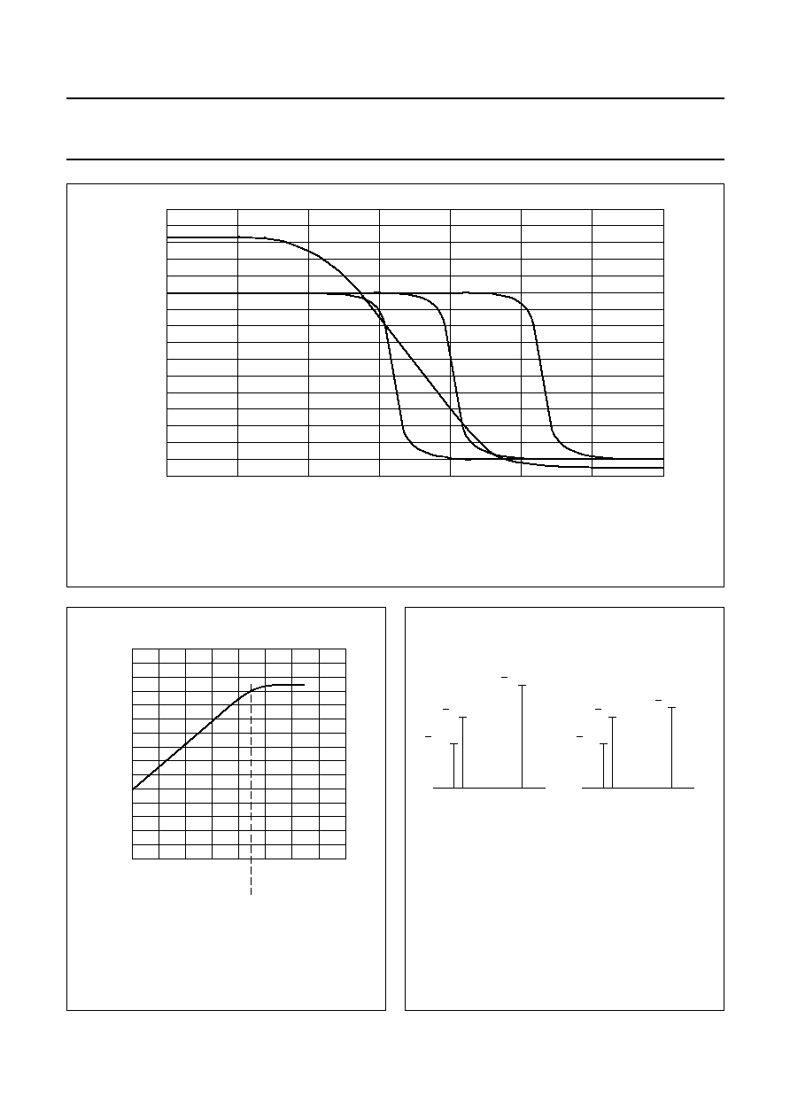
Fig.3 Typical VIF and tuner AGC characteristic.
andbook, full pagewidth
4.5
70
1.0
2.5
2
1.5
3
3.5
4
V28 (V)
MHA061
50
60
0.06
40
0
1.0
2.0
0.6
30
20
6
10
0
60
-
10
gain
(dB)
Ituner
(mA)
VIF input
(1,2)
(mV RMS)
(1)
(2)
(3)
(4)
(1) I
tuner
; R
TOP
= 22 k
.
(2) Gain.
(3) I
tuner
; R
TOP
= 11 k
.
(4) I
tuner
; R
TOP
= 0
.
Fig.4
Typical signal-to-noise ratio as a
function of IF input voltage.
handbook, halfpage
-
60
-
40
-
20
20
80
60
40
20
0
0
0.06
0.6
6
600
60
MED684
S/N
(dB)
Vi (VIF)(rms)(dB)
Vi (VIF)(rms)
(mV)
10
Fig.5 Input signal conditions.
handbook, halfpage
SC CC
PC
SC CC
PC
BLUE
YELLOW
27 dB
13.2 dB
3.2 dB
27 dB
13.2 dB
10 dB
MED685 - 1
SC = sound carrier, with respect to sync level.
CC = chrominance carrier, with respect to sync level.
PC = picture carrier, with respect to sync level.
The sound carrier levels are taking into account
a sound shelf attenuation of 20 dB (SWIF G1962).

1995 Sep 05
18
Philips Semiconductors
Preliminary specification
Multistandard VIF-PLL and
FM-PLL demodulator
TDA9806
Fig.6 Measurement conditions and typical AFC characteristic.
handbook, full pagewidth
V = 5 V
P
V
P
200
100
0
200
100
(
µ
A)
38.5
38.9
39.3 f (MHz)
(source current)
(sink current)
V23
I 23
(V)
4.5
3.5
2.5
1.5
0.5
TDA9806
23
I 23
22 k
22 k
MHA055
Fig.7 Typical video signal levels on output pin 21 (sound carrier off).
handbook, halfpage
1.5 V
1.8 V
2.5 V
white level
2.6 V
zero carrier level
black level
sync level
B/G standard
MHA056
Fig.8 Ripple rejection condition.
handbook, full pagewidth
TDA9806
VP = 5 V
t
VP = 5 V
100 mV
ripple
(f = 70 kHz)
MHA057
1995 Sep 05
19
Philips Semiconductors
Preliminary specification
Multistandard VIF-PLL and
FM-PLL demodulator
TDA9806
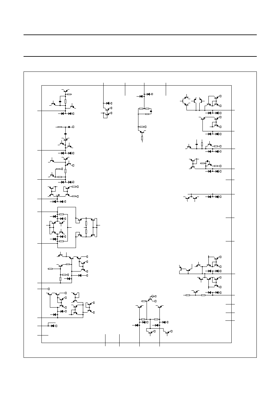
INTERNAL PIN CONFIGURA
TION
handbook, full pagewidth
MHA060
TDA9806
+
20
1.9 mA
10 k
0.5 pF
1.6 k
+
21
2.0 mA
+
1.7 pF
1.7 pF
9 k
+
22
2.2
3.3
2 k
+
23
1 k
1 k
200
µ
A
+
+
2.8 V
420
420
24
25
10 k
10 k
+
+
650
+
20 k
20 k
+
70 k
26
27
GND
+
28
1 mA
+ +
+
29
V
P
+
30
n.c.
16
n.c.
+
17
640
40 k
40 k
10 pF
3.9 k
3.6 V
10 k
3.6 V
19
18
n.c.
2.5 mA
+
9 k
20 k
3.6 V
67
µ
A
+
23
µ
A
VCO
3
5
4
6
7
8
9
+
10
2.5 mA
+
11
+
12
120
14.7 k
25 pF
+
+
2.3 mA
+
13
650
300
µ
A
4.2 k
10 pF
+
+
14
+
15
n.c.
n.c.
32
31
3.6 V
+
2
1.1 k
1.1 k
+
1
0.6
µ
A
k
k
n.c.
n.c.
n.c.
n.c.
n.c.
n.c.
Fig.9 Internal circuitry.
1995 Sep 05
20
Philips Semiconductors
Preliminary specification
Multistandard VIF-PLL and
FM-PLL demodulator
TDA9806
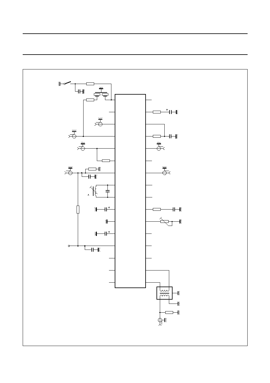
TEST AND APPLICA
TION INFORMA
TION
handbook, full pagewidth
Q 0 50
8.2 pF
2.2
µ
F
Cref
GND
2.2
µ
F
VIF
AGC
22
k
100
nF
10
nF
22 k
AFC
VP
video
output
intercarrier
output
330
n.c.
tuner
AGC
10
nF
SFT
5.5 MHz
560
5.6
k
FM
mute switch
1
2
5
4
3
1:1
50
VIF
input
32
1
TDA9806
n.c.
n.c.
n.c.
n.c.
n.c.
n.c.
TOP
22
k
390
loop
filter
220
nF
CVBS
AF output
5.6
k
10 nF
R
22
µ
F
n.c.
n.c.
n.c.
n.c.
CDEC
x
(1)
31
2
30
3
29
4
28
5
27
6
26
7
25
8
24
9
23
10
22
11
21
12
20
13
19
14
18
15
17
16
MHA058
(1) See note 18 of Chapter "Characteristics".
Fig.10 Test circuit.
1995 Sep 05
21
Philips Semiconductors
Preliminary specification
Multistandard VIF-PLL and
FM-PLL demodulator
TDA9806
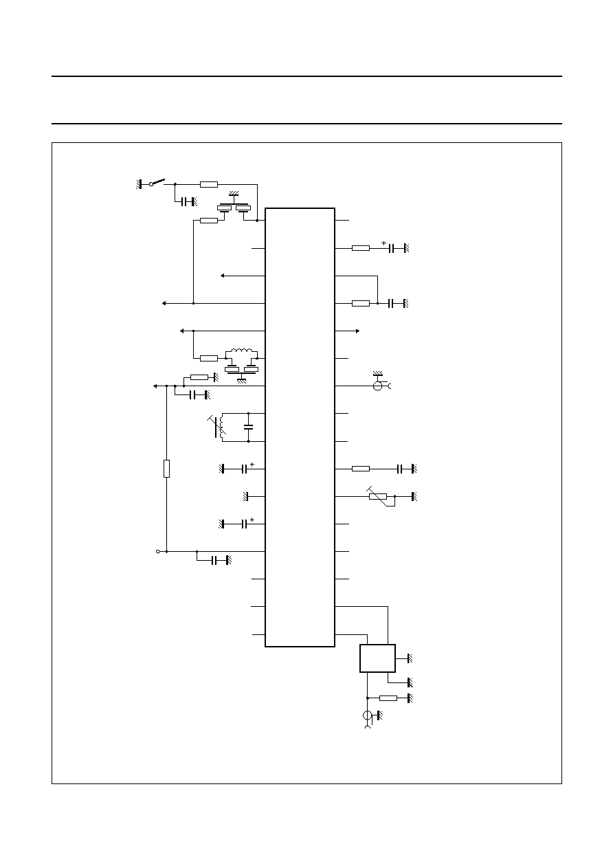
handbook, full pagewidth
8.2 pF
2.2
µ
F
Cref
GND
2.2
µ
F
VIF
AGC
22
k
100
nF
10
nF
22 k
AFC
VP
video
output
intercarrier
output
330
n.c.
tuner
AGC
10
nF
5.5 MHz
560
5.6
k
FM
mute switch
50
IF
input
32
1
TDA9806
n.c.
n.c.
n.c.
n.c.
n.c.
n.c.
n.c.
n.c.
n.c.
TOP
22
k
390
loop
filter
220
nF
CVBS
AF
output
5.6
k
10 nF
R
22
µ
F
n.c.
CDEC
x
(2)
31
2
30
3
29
4
28
5
27
6
26
7
25
8
24
9
23
10
22
11
21
12
20
13
19
14
18
15
17
16
15
µ
H
(1)
SWIF
G1962
MHA059
Fig.11 Application circuit.
(1) Depends on standard.
(2) See note 18 of Chapter "Characteristics".
1995 Sep 05
22
Philips Semiconductors
Preliminary specification
Multistandard VIF-PLL and
FM-PLL demodulator
TDA9806
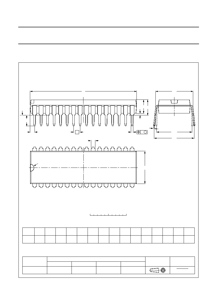
PACKAGE OUTLINE
UNIT
b
1
c
E
e
M
H
L
REFERENCES
OUTLINE
VERSION
EUROPEAN
PROJECTION
ISSUE DATE
IEC
JEDEC
EIAJ
mm
DIMENSIONS (mm are the original dimensions)
SOT232-1
92-11-17
95-02-04
b
max.
w
M
E
e
1
1.3
0.8
0.53
0.40
0.32
0.23
29.4
28.5
9.1
8.7
3.2
2.8
0.18
1.778
10.16
10.7
10.2
12.2
10.5
1.6
4.7
0.51
3.8
M
H
c
(e )
1
M
E
A
L
seating plane
A
1
w
M
b
1
e
D
A
2
Z
32
1
17
16
b
E
pin 1 index
0
5
10 mm
scale
Note
1. Plastic or metal protrusions of 0.25 mm maximum per side are not included.
(1)
(1)
D
(1)
Z
A
max.
1
2
A
min.
A
max.
SDIP32: plastic shrink dual in-line package; 32 leads (400 mil)
SOT232-1

1995 Sep 05
23
Philips Semiconductors
Preliminary specification
Multistandard VIF-PLL and
FM-PLL demodulator
TDA9806
SOLDERING
Introduction
There is no soldering method that is ideal for all IC
packages. Wave soldering is often preferred when
through-hole and surface mounted components are mixed
on one printed-circuit board. However, wave soldering is
not always suitable for surface mounted ICs, or for
printed-circuits with high population densities. In these
situations reflow soldering is often used.
This text gives a very brief insight to a complex technology.
A more in-depth account of soldering ICs can be found in
our
"IC Package Databook" (order code 9398 652 90011).
Soldering by dipping or by wave
The maximum permissible temperature of the solder is
260
∞
C; solder at this temperature must not be in contact
with the joint for more than 5 seconds. The total contact
time of successive solder waves must not exceed
5 seconds.
The device may be mounted up to the seating plane, but
the temperature of the plastic body must not exceed the
specified maximum storage temperature (T
stg max
). If the
printed-circuit board has been pre-heated, forced cooling
may be necessary immediately after soldering to keep the
temperature within the permissible limit.
Repairing soldered joints
Apply a low voltage soldering iron (less than 24 V) to the
lead(s) of the package, below the seating plane or not
more than 2 mm above it. If the temperature of the
soldering iron bit is less than 300
∞
C it may remain in
contact for up to 10 seconds. If the bit temperature is
between 300 and 400
∞
C, contact may be up to 5 seconds.
DEFINITIONS
LIFE SUPPORT APPLICATIONS
These products are not designed for use in life support appliances, devices, or systems where malfunction of these
products can reasonably be expected to result in personal injury. Philips customers using or selling these products for
use in such applications do so at their own risk and agree to fully indemnify Philips for any damages resulting from such
improper use or sale.
Data sheet status
Objective specification
This data sheet contains target or goal specifications for product development.
Preliminary specification
This data sheet contains preliminary data; supplementary data may be published later.
Product specification
This data sheet contains final product specifications.
Limiting values
Limiting values given are in accordance with the Absolute Maximum Rating System (IEC 134). Stress above one or
more of the limiting values may cause permanent damage to the device. These are stress ratings only and operation
of the device at these or at any other conditions above those given in the Characteristics sections of the specification
is not implied. Exposure to limiting values for extended periods may affect device reliability.
Application information
Where application information is given, it is advisory and does not form part of the specification.

Philips Semiconductors ≠ a worldwide company
Argentina: IEROD, Av. Juramento 1992 - 14.b, (1428)
BUENOS AIRES, Tel. (541)786 7633, Fax. (541)786 9367
Australia: 34 Waterloo Road, NORTH RYDE, NSW 2113,
Tel. (02)805 4455, Fax. (02)805 4466
Austria: Triester Str. 64, A-1101 WIEN, P.O. Box 213,
Tel. (01)60 101-1236, Fax. (01)60 101-1211
Belgium: Postbus 90050, 5600 PB EINDHOVEN, The Netherlands,
Tel. (31)40 783 749, Fax. (31)40 788 399
Brazil: Rua do Rocio 220 - 5
th
floor, Suite 51,
CEP: 04552-903-S√O PAULO-SP, Brazil.
P.O. Box 7383 (01064-970),
Tel. (011)821-2333, Fax. (011)829-1849
Canada: PHILIPS SEMICONDUCTORS/COMPONENTS:
Tel. (800) 234-7381, Fax. (708) 296-8556
Chile: Av. Santa Maria 0760, SANTIAGO,
Tel. (02)773 816, Fax. (02)777 6730
China/Hong Kong: 501 Hong Kong Industrial Technology Centre,
72 Tat Chee Avenue, Kowloon Tong, HONG KONG,
Tel. (852)2319 7888, Fax. (852)2319 7700
Colombia: IPRELENSO LTDA, Carrera 21 No. 56-17,
77621 BOGOTA, Tel. (571)249 7624/(571)217 4609,
Fax. (571)217 4549
Denmark: Prags Boulevard 80, PB 1919, DK-2300
COPENHAGEN S, Tel. (032)88 2636, Fax. (031)57 1949
Finland: Sinikalliontie 3, FIN-02630 ESPOO,
Tel. (358)0-615 800, Fax. (358)0-61580 920
France: 4 Rue du Port-aux-Vins, BP317,
92156 SURESNES Cedex,
Tel. (01)4099 6161, Fax. (01)4099 6427
Germany: P.O. Box 10 63 23, 20043 HAMBURG,
Tel. (040)3296-0, Fax. (040)3296 213.
Greece: No. 15, 25th March Street, GR 17778 TAVROS,
Tel. (01)4894 339/4894 911, Fax. (01)4814 240
India: Philips INDIA Ltd, Shivsagar Estate, A Block,
Dr. Annie Besant Rd. Worli, Bombay 400 018
Tel. (022)4938 541, Fax. (022)4938 722
Indonesia: Philips House, Jalan H.R. Rasuna Said Kav. 3-4,
P.O. Box 4252, JAKARTA 12950,
Tel. (021)5201 122, Fax. (021)5205 189
Ireland: Newstead, Clonskeagh, DUBLIN 14,
Tel. (01)7640 000, Fax. (01)7640 200
Italy: PHILIPS SEMICONDUCTORS S.r.l.,
Piazza IV Novembre 3, 20124 MILANO,
Tel. (0039)2 6752 2531, Fax. (0039)2 6752 2557
Japan: Philips Bldg 13-37, Kohnan 2 -chome, Minato-ku, TOKYO 108,
Tel. (03)3740 5130, Fax. (03)3740 5077
Korea: Philips House, 260-199 Itaewon-dong,
Yongsan-ku, SEOUL, Tel. (02)709-1412, Fax. (02)709-1415
Malaysia: No. 76 Jalan Universiti, 46200 PETALING JAYA,
SELANGOR, Tel. (03)750 5214, Fax. (03)757 4880
Mexico: 5900 Gateway East, Suite 200, EL PASO, TX 79905,
Tel. 9-5(800)234-7381, Fax. (708)296-8556
Netherlands: Postbus 90050, 5600 PB EINDHOVEN, Bldg. VB,
Tel. (040)783749, Fax. (040)788399
(From 10-10-1995: Tel. (040)2783749, Fax. (040)2788399)
New Zealand: 2 Wagener Place, C.P.O. Box 1041, AUCKLAND,
Tel. (09)849-4160, Fax. (09)849-7811
Norway: Box 1, Manglerud 0612, OSLO,
Tel. (022)74 8000, Fax. (022)74 8341
Pakistan: Philips Electrical Industries of Pakistan Ltd.,
Exchange Bldg. ST-2/A, Block 9, KDA Scheme 5, Clifton,
KARACHI 75600, Tel. (021)587 4641-49,
Fax. (021)577035/5874546
Philippines: PHILIPS SEMICONDUCTORS PHILIPPINES Inc,
106 Valero St. Salcedo Village, P.O. Box 2108 MCC, MAKATI,
Metro MANILA, Tel. (02)810 0161, Fax. (02)817 3474
Portugal: PHILIPS PORTUGUESA, S.A.,
Rua dr. AntÛnio Loureiro Borges 5, Arquiparque - Miraflores,
Apartado 300, 2795 LINDA-A-VELHA,
Tel. (01)4163160/4163333, Fax. (01)4163174/4163366
Singapore: Lorong 1, Toa Payoh, SINGAPORE 1231,
Tel. (65)350 2000, Fax. (65)251 6500
South Africa: S.A. PHILIPS Pty Ltd.,
195-215 Main Road Martindale, 2092 JOHANNESBURG,
P.O. Box 7430, Johannesburg 2000,
Tel. (011)470-5911, Fax. (011)470-5494.
Spain: Balmes 22, 08007 BARCELONA,
Tel. (03)301 6312, Fax. (03)301 42 43
Sweden: Kottbygatan 7, Akalla. S-164 85 STOCKHOLM,
Tel. (0)8-632 2000, Fax. (0)8-632 2745
Switzerland: Allmendstrasse 140, CH-8027 ZÐRICH,
Tel. (01)488 2211, Fax. (01)481 77 30
Taiwan: PHILIPS TAIWAN Ltd., 23-30F, 66, Chung Hsiao West
Road, Sec. 1. Taipeh, Taiwan ROC, P.O. Box 22978,
TAIPEI 100, Tel. (02)388 7666, Fax. (02)382 4382
Thailand: PHILIPS ELECTRONICS (THAILAND) Ltd.,
209/2 Sanpavuth-Bangna Road Prakanong,
Bangkok 10260, THAILAND,
Tel. (662)398-0141, Fax. (662)398-3319
Turkey: Talatpasa Cad. No. 5, 80640 GÐLTEPE/ISTANBUL,
Tel. (0 212)279 27 70, Fax. (0212)282 67 07
United Kingdom: Philips Semiconductors LTD.,
276 Bath Road, Hayes, MIDDLESEX UB3 5BX,
Tel. (0181)730-5000, Fax. (0181)754-8421
United States: 811 East Arques Avenue, SUNNYVALE,
CA 94088-3409, Tel. (800)234-7381, Fax. (708)296-8556
Uruguay: Coronel Mora 433, MONTEVIDEO,
Tel. (02)70-4044, Fax. (02)92 0601
Internet: http://www.semiconductors.philips.com/ps/
For all other countries apply to: Philips Semiconductors,
International Marketing and Sales, Building BE-p,
P.O. Box 218, 5600 MD EINDHOVEN, The Netherlands,
Telex 35000 phtcnl, Fax. +31-40-724825 (from 10-10-1995: +31-40-2724825)
SCD41
© Philips Electronics N.V. 1995
All rights are reserved. Reproduction in whole or in part is prohibited without the
prior written consent of the copyright owner.
The information presented in this document does not form part of any quotation
or contract, is believed to be accurate and reliable and may be changed without
notice. No liability will be accepted by the publisher for any consequence of its
use. Publication thereof does not convey nor imply any license under patent- or
other industrial or intellectual property rights.
Printed in The Netherlands
533061/1500/01/pp24
Date of release: 1995 Sep 05
Document order number:
9397 750 00307